EP2806512A1 - Connector and electronic system using the same - Google Patents
Connector and electronic system using the same Download PDFInfo
- Publication number
- EP2806512A1 EP2806512A1 EP12866100.6A EP12866100A EP2806512A1 EP 2806512 A1 EP2806512 A1 EP 2806512A1 EP 12866100 A EP12866100 A EP 12866100A EP 2806512 A1 EP2806512 A1 EP 2806512A1
- Authority
- EP
- European Patent Office
- Prior art keywords
- electronic device
- connector
- grounding terminal
- plane
- terminal
- Prior art date
- Legal status (The legal status is an assumption and is not a legal conclusion. Google has not performed a legal analysis and makes no representation as to the accuracy of the status listed.)
- Withdrawn
Links
- 230000004308 accommodation Effects 0.000 claims description 5
- 238000004891 communication Methods 0.000 claims description 5
- 238000000034 method Methods 0.000 claims description 3
- 230000005540 biological transmission Effects 0.000 abstract description 3
- 230000009286 beneficial effect Effects 0.000 abstract 1
- 238000005516 engineering process Methods 0.000 description 4
- 239000004020 conductor Substances 0.000 description 2
- 238000004519 manufacturing process Methods 0.000 description 2
- 230000008054 signal transmission Effects 0.000 description 2
- 230000003628 erosive effect Effects 0.000 description 1
- 239000007769 metal material Substances 0.000 description 1
- 238000012986 modification Methods 0.000 description 1
- 230000004048 modification Effects 0.000 description 1
- 238000003466 welding Methods 0.000 description 1
Images


Classifications
-
- H—ELECTRICITY
- H01—ELECTRIC ELEMENTS
- H01R—ELECTRICALLY-CONDUCTIVE CONNECTIONS; STRUCTURAL ASSOCIATIONS OF A PLURALITY OF MUTUALLY-INSULATED ELECTRICAL CONNECTING ELEMENTS; COUPLING DEVICES; CURRENT COLLECTORS
- H01R13/00—Details of coupling devices of the kinds covered by groups H01R12/70 or H01R24/00 - H01R33/00
- H01R13/646—Details of coupling devices of the kinds covered by groups H01R12/70 or H01R24/00 - H01R33/00 specially adapted for high-frequency, e.g. structures providing an impedance match or phase match
- H01R13/6461—Means for preventing cross-talk
- H01R13/6471—Means for preventing cross-talk by special arrangement of ground and signal conductors, e.g. GSGS [Ground-Signal-Ground-Signal]
-
- H—ELECTRICITY
- H01—ELECTRIC ELEMENTS
- H01R—ELECTRICALLY-CONDUCTIVE CONNECTIONS; STRUCTURAL ASSOCIATIONS OF A PLURALITY OF MUTUALLY-INSULATED ELECTRICAL CONNECTING ELEMENTS; COUPLING DEVICES; CURRENT COLLECTORS
- H01R12/00—Structural associations of a plurality of mutually-insulated electrical connecting elements, specially adapted for printed circuits, e.g. printed circuit boards [PCB], flat or ribbon cables, or like generally planar structures, e.g. terminal strips, terminal blocks; Coupling devices specially adapted for printed circuits, flat or ribbon cables, or like generally planar structures; Terminals specially adapted for contact with, or insertion into, printed circuits, flat or ribbon cables, or like generally planar structures
- H01R12/70—Coupling devices
- H01R12/71—Coupling devices for rigid printing circuits or like structures
- H01R12/72—Coupling devices for rigid printing circuits or like structures coupling with the edge of the rigid printed circuits or like structures
- H01R12/73—Coupling devices for rigid printing circuits or like structures coupling with the edge of the rigid printed circuits or like structures connecting to other rigid printed circuits or like structures
-
- H—ELECTRICITY
- H01—ELECTRIC ELEMENTS
- H01R—ELECTRICALLY-CONDUCTIVE CONNECTIONS; STRUCTURAL ASSOCIATIONS OF A PLURALITY OF MUTUALLY-INSULATED ELECTRICAL CONNECTING ELEMENTS; COUPLING DEVICES; CURRENT COLLECTORS
- H01R13/00—Details of coupling devices of the kinds covered by groups H01R12/70 or H01R24/00 - H01R33/00
- H01R13/646—Details of coupling devices of the kinds covered by groups H01R12/70 or H01R24/00 - H01R33/00 specially adapted for high-frequency, e.g. structures providing an impedance match or phase match
- H01R13/6461—Means for preventing cross-talk
-
- H—ELECTRICITY
- H01—ELECTRIC ELEMENTS
- H01R—ELECTRICALLY-CONDUCTIVE CONNECTIONS; STRUCTURAL ASSOCIATIONS OF A PLURALITY OF MUTUALLY-INSULATED ELECTRICAL CONNECTING ELEMENTS; COUPLING DEVICES; CURRENT COLLECTORS
- H01R13/00—Details of coupling devices of the kinds covered by groups H01R12/70 or H01R24/00 - H01R33/00
- H01R13/40—Securing contact members in or to a base or case; Insulating of contact members
- H01R13/405—Securing in non-demountable manner, e.g. moulding, riveting
Definitions
- the invention relates to a connector and an electronic system using the same and, more particularly, to a high frequency connector and an electronic system using the same.
- coaxial cables are used as connectors in transmission of high frequency signals or connection of different electronic communication products.
- the coaxial cable connector is larger and occupies much space, it is difficult to be applied to a small-sized portable electronic device (such as a phone).
- the architecture of the coaxial cable connector is fixed and is not easy to be changed, it is difficult to be customized for various products.
- the manufacturing cost of the coaxial cable connector is high.
- a coplanar waveguide technology is another common conventional high frequency signal transmission technology.
- the coplanar waveguide technology has a feature that it includes a single plane of transmission lines, that means, a signal line and a grounding line are in the same plane, which makes electronic components connected to each other in series or parallel easily.
- the coplanar waveguide technology makes electric characteristic of the electronic components not easily affected by the thickness of a dielectric plate. Consequently, the manufacturing cost of circuits is greatly reduced, and a circuit layout has more choices.
- a connector used to connect a first electronic device and a second electronic device includes a first grounding terminal, a signal terminal and a second grounding terminal.
- the signal terminal is between the first grounding terminal and the second grounding terminal.
- the first grounding terminal includes a first end and a second end
- the signal terminal includes a third end and a fourth end
- the second grounding terminal includes a fifth end and a sixth end.
- the first end, the third end and the fifth end are electrically connected to a first plane of the first electronic device.
- the second end, the fourth end and the sixth end are electrically connected to a second plane of the second electronic device, respectively.
- the first plane and the second plane are not coplanar.
- An electronic system including a first electronic device, a second electronic device and a connector.
- the first electronic device includes a first plane.
- the second electronic device includes a second plane.
- the first plane and the second plane are not coplanar.
- the connector includes a first grounding terminal, a signal terminal and a second grounding terminal.
- the signal terminal is between the first grounding terminal and the second grounding terminal.
- the first grounding terminal includes a first end and a second end
- the signal terminal includes a third end and a fourth end
- the second grounding terminal includes a fifth end and a sixth end.
- the first end, the third end and the fifth end are electrically connected to a first plane, respectively.
- the second end, the fourth end and the sixth end are electrically connected to a second plane, respectively.
- the first grounding terminal, the signal terminal and the second grounding terminal are made of conducting materials.
- the first grounding terminal and the second grounding terminal are equipotential.
- the signal terminal is a high frequency signal terminal.
- the connector further includes a casing, the first grounding terminal, the signal terminal and the second grounding terminal are partially disposed inside the casing, respectively.
- the second electronic device includes an accommodation slot to accommodate the first electronic device.
- the first electronic device is an electronic communication product.
- the signal terminal is transmitted between the first grounding terminal and the second grounding terminal, so as to transmit a high frequency signal with low noise at a shielding environment.
- the terminal of the connector can be adjusted easily to meets the customized requirements.
- FIG. 1 is a partial perspective showing a first electronic device of an electronic system that is electrically connected to a second electronic device via a connector in an embodiment.
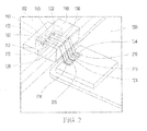
- FIG. 2 is an enlarged view of partial of the connector connecting two electronic devices in FIG. 1 .
- an electronic system 100 includes a first electronic device 102, a second electronic device 200 and a connector 104.
- the first electronic device 102 includes a plurality of first connection points 103
- the second electronic device 200 includes a plurality of second connection points 210.
- the connector 104 includes a first grounding terminal 110, a signal terminal 120 and a second grounding terminal 130.
- the signal terminal 120 is between the first grounding terminal 110 and the second grounding terminal 130.
- the first grounding terminal 110, the signal terminal 120 and the second grounding terminal 130 is made of conducting materials, such as a metal material.
- the first grounding terminal 110 includes a first end 112 and a second end 114.
- the signal terminal 120 includes a third end 122 and a fourth end 124
- the second grounding terminal 130 includes a fifth end 132 and a sixth end 134.
- the first end 112, the third end 122 and the fifth end 132 are electrically connected to the first electronic device 102, respectively.
- the second end 114, the fourth end 124 and the sixth end 134 are electrically connected to the second electronic device 200, respectively.
- the first end 112, the third end 122 and the fifth end 132 are electrically connected to one of the first connection points 103 by welding or other methods, respectively.
- the second end 114, the fourth end 124 and the sixth end 134 are electrically connected to one of the second connection points 210, respectively.
- the second electronic device 200 includes an accommodation slot 220 to accommodate the first electronic device 102.
- the first electronic device 102 is integrated to the second electronic device 200 to have a smooth appearance.
- the first electronic device 102 is an electronic communication product, such as a phone.
- FIG. 3 is a side view of partial of the connector in FIG. 1 .
- the first connection points 103 are at a first plane P10 of the first electronic device 102
- the second connection points 210 are at a second plane P20 of the second electronic device 200.
- the first plane P10 and the second plane P20 are not coplanar. That means, in the embodiment, the connector104 can be connected to connection points at different planes, and signals are transmitted among the connection points at different planes.
- the first end 112, the third end 122 and the fifth end 132 are at the same plane, and they are electrically connected to the first connection points 103 at the first plane P10, respectively.
- the second end 114, the fourth end 124 and the sixth end 134 are at the same plane, and they are electrically connected to the second connection points 210 at the second plane P20, respectively.
- the first grounding terminal 110 and the second grounding terminal 130 may be equipotential.
- the signal terminal 120 may be a high frequency signal terminal used to transmit high frequency signals. Since the signal terminal 120 is between the first grounding terminal 110 and the second grounding terminal 130, the first grounding terminal 110 and the second grounding terminal 130 can be the shields for the signal terminal 120, it can avoid that the signals transmitted by the signal terminal 120 is interfered by external disturbance.
- the first grounding terminal 110 and the second grounding terminal 130 are equipotential, a certain potential difference is maintained between the first grounding terminal 110 and the signal terminal 120, and also between the second grounding terminal 130 and the signal terminal 120. As a result, grounding lines surround a signal line, and then the signal transmission quality of the signal line is maintained, and the loss of signals is avoided.
- the first end 112, the third end 122, the fifth end 132, the second end 114, the fourth end 124 and the sixth end 134 are flat-shaped, which is not limited herein, the shape can be adjusted according to requirements and the space.
- the connector104 further includes a casing 140.
- the first grounding terminal 110, the signal terminal 120 and the second grounding terminal 130 are partially disposed inside the casing 140, respectively.
- the casing 140 can be used to prevent the first grounding terminal 110, the signal terminal 120 and the second grounding terminal 130from moisture erosion, and it can also avoids the reformation of the first grounding terminal 110, the signal terminal 120 and the second grounding terminal 130.
- the signal terminal is between the first grounding terminal and the second grounding terminal, and the first grounding terminal and the second grounding terminal can shield external disturbance to avoid the interference on the high frequency signal transmitted by the signal terminal.
- the terminal of the connector can be adjusted in the three-dimensional stereoscopic space, and thus the connection points at different planes can be connected, which can easily meets the customized requirements.
Landscapes
- Details Of Connecting Devices For Male And Female Coupling (AREA)
- Telephone Set Structure (AREA)
- Coupling Device And Connection With Printed Circuit (AREA)
Abstract
Description
- The invention relates to a connector and an electronic system using the same and, more particularly, to a high frequency connector and an electronic system using the same.
- Conventionally, coaxial cables are used as connectors in transmission of high frequency signals or connection of different electronic communication products. However, since the coaxial cable connector is larger and occupies much space, it is difficult to be applied to a small-sized portable electronic device (such as a phone). On the other hand, since the architecture of the coaxial cable connector is fixed and is not easy to be changed, it is difficult to be customized for various products. Moreover, the manufacturing cost of the coaxial cable connector is high.
- In addition, a coplanar waveguide technology is another common conventional high frequency signal transmission technology. The coplanar waveguide technology has a feature that it includes a single plane of transmission lines, that means, a signal line and a grounding line are in the same plane, which makes electronic components connected to each other in series or parallel easily. Moreover, the coplanar waveguide technology makes electric characteristic of the electronic components not easily affected by the thickness of a dielectric plate. Consequently, the manufacturing cost of circuits is greatly reduced, and a circuit layout has more choices.
- A connector used to connect a first electronic device and a second electronic device is provided. The connector includes a first grounding terminal, a signal terminal and a second grounding terminal. The signal terminal is between the first grounding terminal and the second grounding terminal. The first grounding terminal includes a first end and a second end, the signal terminal includes a third end and a fourth end, the second grounding terminal includes a fifth end and a sixth end. The first end, the third end and the fifth end are electrically connected to a first plane of the first electronic device. The second end, the fourth end and the sixth end are electrically connected to a second plane of the second electronic device, respectively. The first plane and the second plane are not coplanar.
- An electronic system including a first electronic device, a second electronic device and a connector is provided. The first electronic device includes a first plane. The second electronic device includes a second plane. The first plane and the second plane are not coplanar. The connector includes a first grounding terminal, a signal terminal and a second grounding terminal. The signal terminal is between the first grounding terminal and the second grounding terminal. The first grounding terminal includes a first end and a second end, the signal terminal includes a third end and a fourth end, the second grounding terminal includes a fifth end and a sixth end. The first end, the third end and the fifth end are electrically connected to a first plane, respectively. The second end, the fourth end and the sixth end are electrically connected to a second plane, respectively.
- In an embodiment, the first grounding terminal, the signal terminal and the second grounding terminal are made of conducting materials.
- In an embodiment, the first grounding terminal and the second grounding terminal are equipotential.
- In an embodiment, the signal terminal is a high frequency signal terminal.
- In an embodiment, the connector further includes a casing, the first grounding terminal, the signal terminal and the second grounding terminal are partially disposed inside the casing, respectively.
- In an embodiment, the second electronic device includes an accommodation slot to accommodate the first electronic device.
- In an embodiment, the first electronic device is an electronic communication product.
- In conclusion, according to the connector and the electronic device disclosed here in embodiments above, the signal terminal is transmitted between the first grounding terminal and the second grounding terminal, so as to transmit a high frequency signal with low noise at a shielding environment. In addition, the terminal of the connector can be adjusted easily to meets the customized requirements.
- These and other features, aspects and advantages of the present invention will become better understood with regard to the following description, appended claims, and accompanying drawings.
-
-
FIG. 1 is a partial perspective showing that a first electronic device of an electronic system is electrically connected to a second electronic device via a connector in an embodiment; -
FIG. 2 is an enlarged view of partial of the connector inFIG. 1 ; and -
FIG. 3 is a side view of partial of the connector inFIG. 1 . - Reference will now be made in detail to the present preferred embodiments of the invention, examples of which are illustrated in the accompanying drawings. Wherever possible, the same reference numbers are used in the drawings and the description to refer to the same or like parts.
-
FIG. 1 is a partial perspective showing a first electronic device of an electronic system that is electrically connected to a second electronic device via a connector in an embodiment.FIG. 2 is an enlarged view of partial of the connector connecting two electronic devices inFIG. 1 . Please refer toFIG. 1 andFIG. 2 , in the embodiment, anelectronic system 100 includes a firstelectronic device 102, a secondelectronic device 200 and aconnector 104. In the embodiment, the firstelectronic device 102 includes a plurality offirst connection points 103, and the secondelectronic device 200 includes a plurality ofsecond connection points 210. Theconnector 104 includes afirst grounding terminal 110, asignal terminal 120 and asecond grounding terminal 130. Thesignal terminal 120 is between thefirst grounding terminal 110 and thesecond grounding terminal 130. In an embodiment, thefirst grounding terminal 110, thesignal terminal 120 and thesecond grounding terminal 130 is made of conducting materials, such as a metal material. - In the embodiments, the
first grounding terminal 110 includes afirst end 112 and asecond end 114. Thesignal terminal 120 includes athird end 122 and afourth end 124, and thesecond grounding terminal 130 includes afifth end 132 and asixth end 134. Thefirst end 112, thethird end 122 and thefifth end 132 are electrically connected to the firstelectronic device 102, respectively. Thesecond end 114, thefourth end 124 and thesixth end 134 are electrically connected to the secondelectronic device 200, respectively. - In the embodiment, the
first end 112, thethird end 122 and thefifth end 132 are electrically connected to one of thefirst connection points 103 by welding or other methods, respectively. When the firstelectronic device 102 is connected to the secondelectronic device 200, thesecond end 114, thefourth end 124 and thesixth end 134 are electrically connected to one of thesecond connection points 210, respectively. - In an embodiment, the second
electronic device 200 includes anaccommodation slot 220 to accommodate the firstelectronic device 102. In detail, after the firstelectronic device 102 is accommodated in the accommodation slot, the firstelectronic device 102 is integrated to the secondelectronic device 200 to have a smooth appearance. In the embodiment, the firstelectronic device 102 is an electronic communication product, such as a phone. -
FIG. 3 is a side view of partial of the connector inFIG. 1 . Please refer toFIG. 2 andFIG. 3 , thefirst connection points 103 are at a first plane P10 of the firstelectronic device 102, and thesecond connection points 210 are at a second plane P20 of the secondelectronic device 200. The first plane P10 and the second plane P20 are not coplanar. That means, in the embodiment, the connector104 can be connected to connection points at different planes, and signals are transmitted among the connection points at different planes. Additionally, to conform to the coplanar waveguide theory, thefirst end 112, thethird end 122 and thefifth end 132 are at the same plane, and they are electrically connected to the first connection points 103 at the first plane P10, respectively. Similarly, to conform to the coplanar waveguide theory, thesecond end 114, thefourth end 124 and thesixth end 134 are at the same plane, and they are electrically connected to the second connection points 210 at the second plane P20, respectively. - In the embodiment, the
first grounding terminal 110 and thesecond grounding terminal 130 may be equipotential. On the other hand, in the embodiment, thesignal terminal 120 may be a high frequency signal terminal used to transmit high frequency signals. Since thesignal terminal 120 is between thefirst grounding terminal 110 and thesecond grounding terminal 130, thefirst grounding terminal 110 and thesecond grounding terminal 130 can be the shields for thesignal terminal 120, it can avoid that the signals transmitted by thesignal terminal 120 is interfered by external disturbance. In detail, since thefirst grounding terminal 110 and thesecond grounding terminal 130 are equipotential, a certain potential difference is maintained between thefirst grounding terminal 110 and thesignal terminal 120, and also between thesecond grounding terminal 130 and thesignal terminal 120. As a result, grounding lines surround a signal line, and then the signal transmission quality of the signal line is maintained, and the loss of signals is avoided. - In order to increase a contacting area to maintain stability of the electrical connection, in the embodiment, the
first end 112, thethird end 122, thefifth end 132, thesecond end 114, thefourth end 124 and thesixth end 134 are flat-shaped, which is not limited herein, the shape can be adjusted according to requirements and the space. - In the embodiment, the connector104 further includes a
casing 140. Thefirst grounding terminal 110, thesignal terminal 120 and thesecond grounding terminal 130 are partially disposed inside thecasing 140, respectively. Thecasing 140 can be used to prevent thefirst grounding terminal 110, thesignal terminal 120 and the second grounding terminal 130from moisture erosion, and it can also avoids the reformation of thefirst grounding terminal 110, thesignal terminal 120 and thesecond grounding terminal 130. - In conclusion, according to the connector and the electronic system in the embodiments, the signal terminal is between the first grounding terminal and the second grounding terminal, and the first grounding terminal and the second grounding terminal can shield external disturbance to avoid the interference on the high frequency signal transmitted by the signal terminal. In addition, the terminal of the connector can be adjusted in the three-dimensional stereoscopic space, and thus the connection points at different planes can be connected, which can easily meets the customized requirements.
- Although the present invention has been described in considerably detail with reference to certain preferred embodiments thereof, the disclosure is not for limiting the scope of the invention. Persons having ordinary skill in the art may make various modifications and changes without departing from the scope of the invention. Therefore, the scope of the appended claims should not be limited to the description of the preferred embodiments described above.
Claims (12)
- A connector (104) used to connect a first electronic device (102) and a second electronic device (200), characterized by comprising:a first grounding terminal (110) including a first end (112) and a second end (114);a signal terminal (120) including a third end (122) and a fourth end (124); anda second grounding terminal (130) including a fifth end (132) and a sixth end (134), wherein the signal terminal (120) is between the first grounding terminal (110) and the second grounding terminal (130), the first end (112), the third end (122) and the fifth end (132) are electrically connected to a first plane (P10) of the first electronic device (102), respectively, the second end (114), the fourth end (124) and the sixth end (134) are electrically connected to a second plane (P20) of the second electronic device (200), respectively, and the first plane (P10) and the second plane (P20) are not coplanar.
- The connector (104) according to claim 1, characterised in that the first grounding terminal (110) and the second grounding terminal (130) are equipotential.
- The connector (104) according to claim 1, characterized in that the signal terminal (120) is a high frequency signal terminal (120).
- The connector (104) according to claim 1, characterized in that the connector (104) further includes a casing (140), the first grounding terminal (110), the signal terminal (120) and the second grounding terminal (130) are partially disposed inside the casing (140), respectively.
- The connector (104) method according to claim 1, characterized in that the second electronic device (200) includes an accommodation slot (220) to accommodate the first electronic device (102).
- The connector (104) method according to claim 1, characterized in that the first electronic device (102) is an electronic communication product.
- An electronic system (100), characterized by comprising:a first electronic device (102) including a first plane (P10);a second electronic device (200) including a second plane (P20), wherein the first plane (P10) and the second plane (P20) are not coplanar; anda connector (104), including:a first grounding terminal (110) including a first end (112) and a second end (114);a signal terminal (120) including a third end (122) and a fourth end (124); anda second grounding terminal (130) including a fifth end (132) and a sixth end (134), wherein the signal terminal (120) is between the first grounding terminal (110) and the second grounding terminal (130), the first end (112), the third end (122) and the fifth end (132) arc electrically connected to the first plane (P10), respectively, the second end (114), the fourth end (124) and the sixth end (134) are electrically connected to the second plane (P20), respectively.
- The electronic system (100) according to claim 7, characterized in that the first grounding terminal (110) and the second grounding terminal (130) are equipotential.
- The electronic system (100) according to claim 7, characterized in that the signal terminal (120) is a high frequency signal terminal (120).
- The electronic system (100) according to claim 7, characterized in that the connector (104) further includes a casing (140), the first grounding terminal (110), the signal terminal (120) and the second grounding terminal (130) are partially disposed inside the casing (140), respectively.
- The electronic system (100) according to claim 7, characterized in that the second electronic device (200) includes an accommodation slot (220) to accommodate the first electronic device (102).
- The electronic system (100) according to claim 7, characterized in that the first electronic device (102) is an electronic communication product.
Applications Claiming Priority (1)
| Application Number | Priority Date | Filing Date | Title |
|---|---|---|---|
| PCT/CN2012/070577 WO2013107020A1 (en) | 2012-01-19 | 2012-01-19 | Connector and electronic system using the same |
Publications (2)
| Publication Number | Publication Date |
|---|---|
| EP2806512A1 true EP2806512A1 (en) | 2014-11-26 |
| EP2806512A4 EP2806512A4 (en) | 2015-10-07 |
Family
ID=48798505
Family Applications (1)
| Application Number | Title | Priority Date | Filing Date |
|---|---|---|---|
| EP12866100.6A Withdrawn EP2806512A4 (en) | 2012-01-19 | 2012-01-19 | Connector and electronic system using the same |
Country Status (5)
| Country | Link |
|---|---|
| US (1) | US9356397B2 (en) |
| EP (1) | EP2806512A4 (en) |
| JP (1) | JP2015504230A (en) |
| CN (1) | CN104054218A (en) |
| WO (1) | WO2013107020A1 (en) |
Families Citing this family (1)
| Publication number | Priority date | Publication date | Assignee | Title |
|---|---|---|---|---|
| JP2015159092A (en) * | 2014-02-25 | 2015-09-03 | 矢崎総業株式会社 | connection terminal |
Family Cites Families (18)
| Publication number | Priority date | Publication date | Assignee | Title |
|---|---|---|---|---|
| US4600907A (en) * | 1985-03-07 | 1986-07-15 | Tektronix, Inc. | Coplanar microstrap waveguide interconnector and method of interconnection |
| US6215377B1 (en) * | 1998-05-26 | 2001-04-10 | Microsubstrates Corporation | Low cost wideband RF port structure for microwave circuit packages using coplanar waveguide and BGA I/O format |
| AU2003286293A1 (en) * | 2002-12-10 | 2004-06-30 | Koninklijke Philips Electronics N.V. | High density package interconnect power and ground strap and method therefor |
| CN101174718B (en) * | 2003-03-14 | 2012-01-04 | 莫莱克斯公司 | Grouped element transmission channel link with pedestal aspects |
| JP2005064362A (en) | 2003-08-19 | 2005-03-10 | Nec Electronics Corp | Method for manufacturing electronic device, method for manufacturing the same, and method for manufacturing semiconductor device |
| JP2006073721A (en) | 2004-09-01 | 2006-03-16 | Denso Corp | Cooling system |
| KR100821580B1 (en) | 2006-10-12 | 2008-04-15 | 주식회사 하이닉스반도체 | Semiconductor memory device |
| WO2008083167A1 (en) * | 2006-12-29 | 2008-07-10 | Sandisk Corporation | Electrical connector with esd grounding clip |
| CN201038541Y (en) * | 2007-01-17 | 2008-03-19 | 实盈电子(东莞)有限公司 | Multi-faced electric connector |
| CN201072838Y (en) * | 2007-07-18 | 2008-06-11 | 宣德科技股份有限公司 | electronic connector |
| JP2009116698A (en) | 2007-11-07 | 2009-05-28 | Toshiba Corp | Information processing device |
| CN101546918B (en) | 2008-03-25 | 2012-05-30 | 鸿富锦精密工业(深圳)有限公司 | USB charging device and charging method |
| US7906730B2 (en) * | 2008-09-29 | 2011-03-15 | Amphenol Corporation | Ground sleeve having improved impedance control and high frequency performance |
| CN101894054A (en) | 2009-05-21 | 2010-11-24 | 华硕电脑股份有限公司 | Computer system with function of repairing damaged BIOS data and repairing method thereof |
| JP4746694B2 (en) | 2009-08-11 | 2011-08-10 | 株式会社バッファロー | Connected device |
| JP4823352B2 (en) | 2009-12-24 | 2011-11-24 | 株式会社東芝 | Information processing device |
| TWI406390B (en) * | 2010-02-26 | 2013-08-21 | 華東科技股份有限公司 | High density integrated circuit module structure |
| TWI460594B (en) | 2011-02-11 | 2014-11-11 | Via Tech Inc | Adaptive usb charging method and system |
-
2012
- 2012-01-19 CN CN201280067295.3A patent/CN104054218A/en active Pending
- 2012-01-19 JP JP2014552461A patent/JP2015504230A/en active Pending
- 2012-01-19 WO PCT/CN2012/070577 patent/WO2013107020A1/en not_active Ceased
- 2012-01-19 EP EP12866100.6A patent/EP2806512A4/en not_active Withdrawn
- 2012-01-19 US US14/373,011 patent/US9356397B2/en active Active
Also Published As
| Publication number | Publication date |
|---|---|
| US20150303621A1 (en) | 2015-10-22 |
| CN104054218A (en) | 2014-09-17 |
| US9356397B2 (en) | 2016-05-31 |
| JP2015504230A (en) | 2015-02-05 |
| WO2013107020A1 (en) | 2013-07-25 |
| EP2806512A4 (en) | 2015-10-07 |
Similar Documents
| Publication | Publication Date | Title |
|---|---|---|
| US10777936B2 (en) | Electrical device having a ground termination component with strain relief | |
| US11121508B2 (en) | Coaxial cable male connector for transmitting super-high frequency signals | |
| US7677927B2 (en) | High bandwidth connector | |
| US20120064762A1 (en) | Terminal structure of coaxial cable, connector, and substrate unit | |
| US11424580B2 (en) | Compact coaxial cable connector for transmitting super high frequency signals | |
| US7841898B1 (en) | Connector adapter | |
| JP2016207422A (en) | Communication connector | |
| TWI734514B (en) | Compact connector for transmitting super high frequency signal | |
| US20160203887A1 (en) | Shielded electrical cable | |
| US9356397B2 (en) | Connector and electronic system using the same | |
| US11502465B2 (en) | Electrical distributor device, signal transmission system and method of making an electrical distributor device | |
| CN112086785B (en) | Compact connectors for transmitting UHF signals | |
| US6739883B1 (en) | Cable end connector assembly | |
| US8715000B2 (en) | Connector assembly | |
| US9786414B2 (en) | Cable | |
| TWI460926B (en) | Connector and electronic system using the same | |
| US9082526B2 (en) | Shielded electrical signal cable | |
| JP5905319B2 (en) | Receiving machine | |
| JP5818449B2 (en) | Noise shielding mechanism | |
| CN110600944A (en) | Electric connector structure | |
| WO2016110599A1 (en) | Connector for an electric harness conducting electric signals with a frequency of not more than 30khz |
Legal Events
| Date | Code | Title | Description |
|---|---|---|---|
| PUAI | Public reference made under article 153(3) epc to a published international application that has entered the european phase |
Free format text: ORIGINAL CODE: 0009012 |
|
| 17P | Request for examination filed |
Effective date: 20140717 |
|
| AK | Designated contracting states |
Kind code of ref document: A1 Designated state(s): AL AT BE BG CH CY CZ DE DK EE ES FI FR GB GR HR HU IE IS IT LI LT LU LV MC MK MT NL NO PL PT RO RS SE SI SK SM TR |
|
| DAX | Request for extension of the european patent (deleted) | ||
| RA4 | Supplementary search report drawn up and despatched (corrected) |
Effective date: 20150902 |
|
| RIC1 | Information provided on ipc code assigned before grant |
Ipc: H01R 13/405 20060101ALN20150828BHEP Ipc: H01R 12/73 20110101ALI20150828BHEP Ipc: H01R 13/646 20110101AFI20150828BHEP |
|
| 17Q | First examination report despatched |
Effective date: 20170825 |
|
| STAA | Information on the status of an ep patent application or granted ep patent |
Free format text: STATUS: THE APPLICATION HAS BEEN WITHDRAWN |
|
| 18W | Application withdrawn |
Effective date: 20171130 |