EP2806306A1 - Wide-viewing-angle liquid crystal display panel, color film base plate and manufacturing method thereof as well as display device - Google Patents
Wide-viewing-angle liquid crystal display panel, color film base plate and manufacturing method thereof as well as display device Download PDFInfo
- Publication number
- EP2806306A1 EP2806306A1 EP12866358.0A EP12866358A EP2806306A1 EP 2806306 A1 EP2806306 A1 EP 2806306A1 EP 12866358 A EP12866358 A EP 12866358A EP 2806306 A1 EP2806306 A1 EP 2806306A1
- Authority
- EP
- European Patent Office
- Prior art keywords
- color filter
- slit electrode
- efficiency
- electrode
- substrate
- Prior art date
- Legal status (The legal status is an assumption and is not a legal conclusion. Google has not performed a legal analysis and makes no representation as to the accuracy of the status listed.)
- Granted
Links
Images

Classifications
-
- G—PHYSICS
- G02—OPTICS
- G02F—OPTICAL DEVICES OR ARRANGEMENTS FOR THE CONTROL OF LIGHT BY MODIFICATION OF THE OPTICAL PROPERTIES OF THE MEDIA OF THE ELEMENTS INVOLVED THEREIN; NON-LINEAR OPTICS; FREQUENCY-CHANGING OF LIGHT; OPTICAL LOGIC ELEMENTS; OPTICAL ANALOGUE/DIGITAL CONVERTERS
- G02F1/00—Devices or arrangements for the control of the intensity, colour, phase, polarisation or direction of light arriving from an independent light source, e.g. switching, gating or modulating; Non-linear optics
- G02F1/01—Devices or arrangements for the control of the intensity, colour, phase, polarisation or direction of light arriving from an independent light source, e.g. switching, gating or modulating; Non-linear optics for the control of the intensity, phase, polarisation or colour
- G02F1/13—Devices or arrangements for the control of the intensity, colour, phase, polarisation or direction of light arriving from an independent light source, e.g. switching, gating or modulating; Non-linear optics for the control of the intensity, phase, polarisation or colour based on liquid crystals, e.g. single liquid crystal display cells
- G02F1/133—Constructional arrangements; Operation of liquid crystal cells; Circuit arrangements
- G02F1/1333—Constructional arrangements; Manufacturing methods
- G02F1/1335—Structural association of cells with optical devices, e.g. polarisers or reflectors
- G02F1/133509—Filters, e.g. light shielding masks
- G02F1/133514—Colour filters
-
- G—PHYSICS
- G02—OPTICS
- G02F—OPTICAL DEVICES OR ARRANGEMENTS FOR THE CONTROL OF LIGHT BY MODIFICATION OF THE OPTICAL PROPERTIES OF THE MEDIA OF THE ELEMENTS INVOLVED THEREIN; NON-LINEAR OPTICS; FREQUENCY-CHANGING OF LIGHT; OPTICAL LOGIC ELEMENTS; OPTICAL ANALOGUE/DIGITAL CONVERTERS
- G02F1/00—Devices or arrangements for the control of the intensity, colour, phase, polarisation or direction of light arriving from an independent light source, e.g. switching, gating or modulating; Non-linear optics
- G02F1/01—Devices or arrangements for the control of the intensity, colour, phase, polarisation or direction of light arriving from an independent light source, e.g. switching, gating or modulating; Non-linear optics for the control of the intensity, phase, polarisation or colour
- G02F1/13—Devices or arrangements for the control of the intensity, colour, phase, polarisation or direction of light arriving from an independent light source, e.g. switching, gating or modulating; Non-linear optics for the control of the intensity, phase, polarisation or colour based on liquid crystals, e.g. single liquid crystal display cells
- G02F1/133—Constructional arrangements; Operation of liquid crystal cells; Circuit arrangements
- G02F1/1333—Constructional arrangements; Manufacturing methods
- G02F1/1343—Electrodes
- G02F1/134309—Electrodes characterised by their geometrical arrangement
-
- G—PHYSICS
- G02—OPTICS
- G02F—OPTICAL DEVICES OR ARRANGEMENTS FOR THE CONTROL OF LIGHT BY MODIFICATION OF THE OPTICAL PROPERTIES OF THE MEDIA OF THE ELEMENTS INVOLVED THEREIN; NON-LINEAR OPTICS; FREQUENCY-CHANGING OF LIGHT; OPTICAL LOGIC ELEMENTS; OPTICAL ANALOGUE/DIGITAL CONVERTERS
- G02F1/00—Devices or arrangements for the control of the intensity, colour, phase, polarisation or direction of light arriving from an independent light source, e.g. switching, gating or modulating; Non-linear optics
- G02F1/01—Devices or arrangements for the control of the intensity, colour, phase, polarisation or direction of light arriving from an independent light source, e.g. switching, gating or modulating; Non-linear optics for the control of the intensity, phase, polarisation or colour
- G02F1/13—Devices or arrangements for the control of the intensity, colour, phase, polarisation or direction of light arriving from an independent light source, e.g. switching, gating or modulating; Non-linear optics for the control of the intensity, phase, polarisation or colour based on liquid crystals, e.g. single liquid crystal display cells
- G02F1/133—Constructional arrangements; Operation of liquid crystal cells; Circuit arrangements
- G02F1/1333—Constructional arrangements; Manufacturing methods
- G02F1/1335—Structural association of cells with optical devices, e.g. polarisers or reflectors
- G02F1/133509—Filters, e.g. light shielding masks
- G02F1/133514—Colour filters
- G02F1/133516—Methods for their manufacture, e.g. printing, electro-deposition or photolithography
-
- G—PHYSICS
- G02—OPTICS
- G02F—OPTICAL DEVICES OR ARRANGEMENTS FOR THE CONTROL OF LIGHT BY MODIFICATION OF THE OPTICAL PROPERTIES OF THE MEDIA OF THE ELEMENTS INVOLVED THEREIN; NON-LINEAR OPTICS; FREQUENCY-CHANGING OF LIGHT; OPTICAL LOGIC ELEMENTS; OPTICAL ANALOGUE/DIGITAL CONVERTERS
- G02F1/00—Devices or arrangements for the control of the intensity, colour, phase, polarisation or direction of light arriving from an independent light source, e.g. switching, gating or modulating; Non-linear optics
- G02F1/01—Devices or arrangements for the control of the intensity, colour, phase, polarisation or direction of light arriving from an independent light source, e.g. switching, gating or modulating; Non-linear optics for the control of the intensity, phase, polarisation or colour
- G02F1/13—Devices or arrangements for the control of the intensity, colour, phase, polarisation or direction of light arriving from an independent light source, e.g. switching, gating or modulating; Non-linear optics for the control of the intensity, phase, polarisation or colour based on liquid crystals, e.g. single liquid crystal display cells
- G02F1/133—Constructional arrangements; Operation of liquid crystal cells; Circuit arrangements
- G02F1/1333—Constructional arrangements; Manufacturing methods
- G02F1/1343—Electrodes
- G02F1/134309—Electrodes characterised by their geometrical arrangement
- G02F1/134372—Electrodes characterised by their geometrical arrangement for fringe field switching [FFS] where the common electrode is not patterned
Definitions
- Embodiments of the present invention relate to a wide view angle liquid crystal display (LCD) panel, a color filter substrate, a manufacturing method thereof, and a display device.
- LCD liquid crystal display
- LCD panels with narrow viewing angles have been gradually replaced by wide view angle LCD panels.
- the traditional wide view angle LCD panels comprise fringe field switching (FFS) wide view angle LCD panels, vertical alignment (VA) wide view angle LCD panels, and in-plane switching (IPS) hard-screen wide view angle LCD panels.
- FFS fringe field switching
- VA vertical alignment
- IPS in-plane switching
- the common points among the three types of wide view angle LCD panels lie in that: an electric field between a common electrode and a pixel electrode on an array substrate is employed to drive liquid crystals to rotate, and the rotation degree of the liquid crystals is adjusted by the control of the magnitude of the electric field, and thus the wide view angle LCD panel can be achieved.
- each sub-pixel comprises a common electrode and a pixel electrode arranged on an array substrate.
- one electrode of the two electrodes is a planar electrode
- the other electrode is a slit electrode.
- the slit electrode is arranged above the planar electrode and is opposite to a color filter substrate.
- Color filters on the color filter substrate are arranged according to the sub-pixels and correspond to the slit electrode of the corresponding sub-pixels on the array substrate.
- an electric field is formed between a slit electrode 2 and a underlying planar electrode 3 on the array substrate 1 and drives the liquid crystals to rotate.
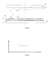
- an electric field (as shown by equipotential lines 4 in FIG. 1A ) between edges of a slit (the part on the slit electrode 2, without filled patterns, is a slit) and the planar electrode 3 is the strongest, and the rotation degree of the liquid crystals is the highest and the liquid crystal (LC) efficiency is the highest here.
- An electric field (as shown by the equipotential lines 4 in FIG.
- the array substrate 1 suffers the phenomenon of nonuniform light transmittance. That is to say, the light transmittance is high at the place with high LC efficiency and low at the place with low LC efficiency.
- the light transmittance of a color filter 6 on the color filter substrate 5, corresponding to the slit electrode 2 is different at different places, the light transmittance of the FFS wide view angle LCD panel is finally varied along with the variation of the LC efficiency. Therefore, the light transmittance of the FFS wide view angle LCD panel suffers loss and become nonuniform accordingly, and thus pictures displayed by the FFS wide view angle LCD panel have bright and dark stripes, and consequently the display effect is poor.
- the traditional wide view angle LCD panel has the disadvantages of nonuniform light transmittance and poor display effect.
- the embodiments of the present invention provide a wide view angle LCD panel, a color filter substrate, a manufacturing method thereof, and a display device, capable of solving the problems of nonuniform light transmittance and poor display effect in the traditional wide view angle LCD panels.
- An embodiment of the present invention provides a wide view angle LCD panel, which comprises an array substrate and a color filter substrate, the array substrate comprises a planar electrode and a slit electrode, which are overlapped to and insulated with each other and configured to produce an electric field capable of driving liquid crystal molecules to rotate;
- the color filter substrate comprises a transparent substrate and a color filter, in which the transparent substrate is arranged opposite to one side of the array substrate, provided with the planar electrode and the slit electrode, and the color filter is arranged on the transparent substrate and corresponds to the slit electrode; and a ratio between light transmittance T1 of any one position on the color filter and light transmittance T2 of any other position on the color filter is equal to a ratio between LC efficiency X2 at a position, corresponding to the any other position, on the slit electrode and LC efficiency X1 at a position, corresponding to the any one position, on the slit electrode.
- the color filter is a first color filter with a same color depth at any position, and a ratio between a thickness H1 at any one position on the first color filter and a thickness H2 at any other position on the first color filter is equal to the ratio between the LC efficiency X1' at the position, corresponding to the any one position, on the slit electrode and the LC efficiency X2' at the position, corresponding to the any other position, on the slit electrode; or the color filter is a second color filter with a same thickness at any position, and a ratio between ink density N1 at any one position on the second color filter and the ink density N2 at any other position on the second color filter is equal to the LC efficiency X1" at the position, corresponding to the any one position, on the slit electrode and the LC efficiency X2" at the position, corresponding to the any other position, on the slit electrode.
- the planar electrode is a pixel electrode, and the slit electrode is a common electrode; or, the planar electrode is a common electrode, and the slit electrode is a pixel electrode.
- An embodiment of the present invention provides a method for manufacturing a wide view angle LCD panel, comprising: manufacturing an array substrate comprising a planar electrode and a slit electrode, which are overlapped and insulated with each other and configured to produce an electric field capable of driving liquid crystal molecules to rotate; manufacturing a color filter substrate comprising a transparent substrate and a color filter arranged on the transparent substrate; and arranging the array substrate and the color filter substrate to be opposite to each other, in which one side of the array substrate, provided with the planar electrode and the slit electrode, is opposite to the color filter substrate; after the array substrate and the color filter substrate are arranged opposite to each other, the color filter corresponds to the slit electrode on the array substrate, and a ratio between light transmittance T1 of any one position on the color filter and light transmittance T2 of any other position on the color filter is equal to a ratio between LC efficiency X2 at a position, corresponding to the any other position, on the slit electrode and LC efficiency X1 at a position, corresponding to
- manufacturing of the color filter substrate comprises: forming a first color filter, with a same color depth at any position, on the transparent substrate, in which a ratio between a thickness H1 at any one position on the first color filter and a thickness H2 at any other position on the first color filter is equal to the ratio between the LC efficiency X1' at the position, corresponding to the any one position, on the slit electrode and the LC efficiency X2' at the position, corresponding to the any other position, on the slit electrode; or, forming a second color filter, with a same thickness at any position, on the transparent substrate, in which a ratio between ink density N1 at any one position on the second color filter and the ink density N2 at any other position on the second color filter is equal to the LC efficiency X1" at the position, corresponding to the any one position, on the slit electrode and the LC efficiency X2" at the position, corresponding to the any other position, on the slit electrode.
- An embodiment of the present invention provides a color filter substrate, which is applied to a wide view angle LCD panel.
- the wide view angle LCD panel comprises an array substrate and the color filter substrate, the array substrate comprises a planar electrode and a slit electrode, which are overlapped to and insulated with each other and configured to produce an electric field capable of driving liquid crystal molecules to rotate, and the color filter substrate comprises a transparent substrate and a color filter arranged on the transparent substrate, in which after the array substrate and the color filter substrate are arranged opposite to each other, the color filter corresponds to the slit electrode on the array substrate, and a ratio between light transmittance T1 of any one position on the color filter and light transmittance T2 of any other position on the color filter is equal to a ratio between LC efficiency X2 at a position, corresponding to the any other position, on the slit electrode and LC efficiency X1 at a position, corresponding to the any one position, on the slit electrode.
- An embodiment of the present invention provides a method for manufacturing a color filter substrate, wherein the color filter substrate is applied to a wide view angle LCD panel.
- the wide view angle LCD panel comprises an array substrate comprising a planar electrode and a slit electrode, which are overlapped to and insulated with each other and configured to produce an electric field capable of driving liquid crystal molecules to rotate.
- the manufacturing method comprises: forming a color filter on a transparent substrate, in which after the array substrate and the color filter substrate are arranged opposite to each other, the color filter corresponds to the slit electrode on the array substrate, and a ratio between light transmittance T1 of any one position on the color filter and light transmittance T2 of any other position on the color filter is equal to a ratio between LC efficiency X2 at a position, corresponding to the any other position, on the slit electrode and LC efficiency X1 at a position, corresponding to the any one position, on the slit electrode.
- An embodiment of the present invention further provides a display device employing the foregoing wide view angle LCD panel.
- the light transmittance at any one position on the color filter of the color filter substrate is in a compensation relationship with the LC efficiency at a position, corresponding to the any one position, on the slit electrode.
- the LC efficiency at the position, corresponding to the any one position, on the slit electrode is large, the light transmittance at the any one position on the color filter is small; and when the LC efficiency at the position, corresponding to the any one position, on the slit electrode is small, the light transmittance at the any one position on the color filter is large.
- the final compensation effect is that the light transmittance at any position of the wide view angle LCD panel is made high and uniform. Compared with the traditional wide view angle LCD panel, the phenomenon of bright and dark stripes will not occur, and thus the display effect can be improved.
- the display device provided by the embodiment of the present invention has the foregoing effect due to the adoption of the foregoing wide view angle LCD panel.
- the array substrate 10 comprises a transparent substrate 15, and a planar electrode 11 and a slit electrode 12, which are formed on the transparent substrate 15 and overlapped to and insulated with each other.
- the planar electrode 11 and the slit electrode 12 as shown in FIG. 2A for instance, belong to one sub-pixel and are configured to produce an electric field capable of driving liquid crystal molecules above the electrodes.
- the color filter substrate 20 comprises a transparent substrate 21 and a color filter 22; the transparent substrate 21 is arranged opposite to one side of the array substrate 10, provided with the planar electrode 11 and the slit electrode 12; the color filter 22 is arranged on the transparent substrate 21 and corresponds to the slit electrode 12; and the color filter 22, for instance, also belongs to one sub-pixel, and for instance, is a red, green or blue color filter. Color filters are, for instance, separated from each other through black matrixes (not shown).
- the ratio (T1/T2) between the light transmittance T1 at any one position on the color filter 22 and the light transmittance T2 at any other position on the color filter 22 is equal to the ratio (X2/X1) between the LC efficiency X2 at a position, corresponding to the any other position, on the slit electrode 12 and the LC efficiency X1 at a position, corresponding to the any one position, on the slit electrode 12.
- the light transmittance at any one position on the color filter of the color filter substrate is in compensation relationship with the LC efficiency at a position, corresponding to the any one position, on the slit electrode. That is to say, when the LC efficiency at the position, corresponding to the any one position, on the slit electrode is large, the light transmittance at the any one position on the color filter is small; and when the LC efficiency at the position, corresponding to the any one position, on the slit electrode is small, the light transmittance at the any one position on the color filter is large.
- the final compensation effect is that the light transmittance at any position of the wide view angle LCD panel is made high and uniform (as shown in FIG. 2B ). Compared with the traditional wide view angle LCD panel, the phenomenon of bright and dark stripes will not occur, and thus the display effect can be improved.
- the color filter may also be either color filter of the following two kinds of the color filters.
- the color filter may be specifically a first color filter with the same color depth at any position, namely the color depth of the first color filter 221 is the same on the entire plane.
- the first color filter may be generally produced by a mask process.
- the light transmittance of the first color filter is controlled by the thickness.
- the color filter may also be specifically a second color filter 222 with the same thickness at any position.
- the second color filter may be produced by an inkjet process or a print process.
- the light transmittance of the second color filter is controlled by the ink density.
- the planar electrode is a pixel electrode, and the slit electrode is a common electrode; or, the planar electrode is a common electrode, and the slit electrode is a pixel electrode.
- the pixel electrode is connected with a switching element (e.g., a TFT) of a corresponding sub-pixel and applied with a data voltage; and the common electrode is connected with a common electrode wire and applied with a common voltage.
- the array substrate and/or a transparent substrate of the color filter substrate may be a glass substrate, a quartz substrate, a plastic substrate or the like.
- an embodiment of the present invention further provides a method for manufacturing a wide view angle LCD panel, which comprises the following steps:
- the array substrate and the color filter substrate which are arranged opposite to each other form a liquid crystal cell through a sealant; liquid crystal materials are filled between the array substrate and the color filter substrate; and the liquid crystal cell is sealed to obtain a liquid crystal panel.
- the light transmittance at any one position on the color filter of the color filter substrate is in compensation relationship with the LC efficiency at a position, corresponding to the any one position, on the slit electrode. That is to say, when the LC efficiency at the position, corresponding to the any one position, on the slit electrode is large, the light transmittance at the any one position on the color filter is small; and when the LC efficiency at the position, corresponding to the any one position, on the slit electrode is small, the light transmittance at the any one position on the color filter is large.
- the final compensation effect is that the light transmittance at any position of the wide view angle LCD panel is made high and uniform. Compared with the traditional wide view angle LCD panel, the phenomenon of bright and dark stripes will not occur, and thus the display effect can be improved.
- the step S42 may be specifically implemented in either mode of the following two modes.
- a first color filter with the same color depth at any position is formed on the transparent substrate.
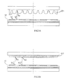
- the ratio between the thickness H1 at any one position on the first color filter and the thickness H2 at any other position on the first color filter is equal to the ratio between the LC efficiency X1' at a position, corresponding to the any one position, on the slit electrode and the LC efficiency X2' at a position, corresponding to the any other position, on the slit electrode (as shown in FIG. 3A ).
- the first mode can be implemented by a mask process or a semi-transparent mask process.
- the thickness at any position on the first color filter is inversely proportional to the light transmittance at the position.
- the light transmittance is controlled by the thickness.
- the ratio between the LC efficiency at the position A1 on the slit electrode and the LC efficiency at the position A2 on the slit electrode is 1:0.8, and hence the ratio between the light transmittance at a position B1 (corresponding to the position A1) on the first color filter and the light transmittance at a position B2 (corresponding to the position A2) on the first color filter is 0.8:1; and in view of the thickness, the ratio between the thickness at the position B1 and the thickness at the position B2 should be made 1:0.8.
- the ratio between the exposure amount at the position B1 and the exposure amount at the position B2 can be set to be 1:0.8. Therefore, after the exposure process and the subsequent processes such as development and baking, the ratio between the light transmittance at the position B1 on the first color filter and the light transmittance at the position B2 on the first color filter is 0.8:1 and is equal to the ratio between the LC efficiency at the position A2 on the slit electrode and the LC efficiency at the position A1 on the slit electrode.
- a second color filter with the same thickness at any position is formed on the transparent substrate.
- the ratio between the ink density N1 at any one position on the second color filter and the ink density N2 at any other position on the second color filter is equal to the ratio between the LC efficiency X1" at a position, corresponding to the any one position, on the slit electrode and the LC efficiency X2" at a position, corresponding to the any other position, on the slit electrode (as shown in FIG. 3B ).
- the second mode may be implemented by an inkjet process or a print process.
- the color depth at any position on the second color filter is inversely proportional to the light transmittance.
- the light transmittance is controlled by the color depth.
- the ratio between the LC efficiency at the position A1 on the slit electrode and the LC efficiency at the position A2 on the slit electrode is 1:0.8, and hence the ratio between the light transmittance at a position C1 (corresponding to the position A1) on the first color filter and the light transmittance at a position C2 (corresponding to the position A2) on the second color filter is 0.8:1; and in view of the color depth, the ratio between the color depth at the position C1 and the color depth at the position C2 should be made 1:0.8.
- the ratio between the ink density at the position C1 and the ink density at the position C2 can be set to be 1:0.8. Therefore, the ratio between the light transmittance at the position C1 on the second color filter and the light transmittance at the position C2 on the second color filter is 0.8:1 and is equal to the ratio between the LC efficiency at the position A2 on the slit electrode and the LC efficiency at the position A1 on the slit electrode.
- an embodiment of the present invention further provides a color filter substrate, which is applied to a wide view angle LCD panel.
- the wide view angle LCD panel comprises an array substrate, the array substrate comprises a planar electrode and a slit electrode, which are overlapped to and insulated with each other and configured to produce an electric field capable of driving liquid crystal molecules to rotate.
- the color filter substrate comprises a transparent substrate and a color filter arranged on the transparent substrate.
- the color filter corresponds to the slit electrode on the array substrate, and the ratio between the light transmittance T1 at any one position on the color filter and the light transmittance T2 at any other position on the color filter is equal to the ratio between the LC efficiency X2 at a position, corresponding to the any other position, on the slit electrode and the LC efficiency X1 at a position, corresponding to the any one position, on the slit electrode (as for the specific structure, see the part of the color filter substrate in FIG. 2A ).
- the color filter substrate provided by the embodiment of the present invention can be applied to the foregoing appropriate wide view angle LCD panel.
- the light transmittance at any one position on the color filter of the color filter substrate is in compensation relationship with the LC efficiency at a position, corresponding to the any one position, on the slit electrode. That is to say, when the LC efficiency at the position, corresponding to the any one position, on the slit electrode is large, the light transmittance at the any one position on the color filter is small; and when the LC efficiency at the position, corresponding to the any one position, on the slit electrode is small, the light transmittance at the any one position on the color filter is large.
- the final compensation effect is that the light transmittance at any position of the wide view angle LCD panel is made high and uniform. Compared with the traditional wide view angle LCD panel, the phenomenon of bright and dark stripes will not occur, and thus the display effect can be improved.
- the color filter may also be divided into a first color filter and a second color filter.
- first color filter and second color filter For the relevant details, see the forgoing relevant recitations of the first color filter and the second color filter, which will not be further repeated herein.
- the embodiment of the present invention further provides a method for manufacturing the aforesaid color filter substrate, and the color filter substrate is applied to a wide view angle LCD panel.
- the wide view angle LCD panel comprises an array substrate comprising a planar electrode and a slit electrode, which are overlapped to and insulated with each other and configured to produce an electric field capable of driving liquid crystal molecules to rotate.
- the manufacturing method comprises: forming a color filter on a transparent substrate, in which after the array substrate and the color filter substrate are arranged opposite to each other, the color filter corresponds to the slit electrode on the array substrate, and the ratio between the light transmittance T1 at any one position on the color filter and the light transmittance T2 at any other position on the color filter can be equal to the ratio between the LC efficiency X2 at a position, corresponding to the any other position, on the slit electrode and the LC efficiency X1 at a position, corresponding to the any one position, on the slit electrode.
- the color filter substrate manufactured by the manufacturing method provided by the embodiment of the present invention can be applied to the foregoing appropriate wide view angle LCD panel.
- the light transmittance at any one position on the color filter of the color filter substrate is in compensation relationship with the LC efficiency at a position, corresponding to the any one position, on the slit electrode. That is to say, when the LC efficiency at the position, corresponding to the any one position, on the slit electrode is large, the light transmittance at the any one position on the color filter is small; and when the LC efficiency at the position, corresponding to the any one position, on the slit electrode is small, the light transmittance at the any one position on the color filter is large.
- the final compensation effect is that the light transmittance at any position of the wide view angle LCD panel is made high and uniform. Compared with the traditional wide view angle LCD panel, the phenomenon of bright and dark stripes will not occur, and thus the display effect can be improved.
- the step of "forming the color filter on the transparent substrate” may also be implemented in the aforesaid specific implementation mode (the first mode and the second mode) the same with the step S42.
- the first mode and the second mode the same with the step S42.
- the method for manufacturing the color filter substrate may further comprise the step of forming a black matrix on the transparent substrate in all the steps of the method for manufacturing the color filter substrate in the embodiment of the present invention.
- the details of the method for forming the black matrix please refer to the art of state, which will not be further repeated herein.
- a planar electrode refers to an electrode which is in a planar shape
- a slit electrode refers to a planar electrode in which slits are formed
- a plurality of the slit electrode are formed on one array substrate
- the color filters are arranged according to the sub-pixels, and the light of a certain color can pass through the color filter
- a plurality of the color filters are arranged on one color filter substrate and correspond to the slit electrodes one by one
- a liquid crystal layer can be disposed between the array substrate and the color filter substrate in the embodiment of the present invention.
- the embodiment of the present invention provides a display device employing the foregoing wide view angle LCD panel.
- the display device may be a mobile phone, a notebook computer, a television, a tablet, a navigator or any device having the display function.
Landscapes
- Physics & Mathematics (AREA)
- Nonlinear Science (AREA)
- Mathematical Physics (AREA)
- Chemical & Material Sciences (AREA)
- Crystallography & Structural Chemistry (AREA)
- General Physics & Mathematics (AREA)
- Optics & Photonics (AREA)
- Geometry (AREA)
- Liquid Crystal (AREA)
- Engineering & Computer Science (AREA)
- Manufacturing & Machinery (AREA)
Abstract
Description
- Embodiments of the present invention relate to a wide view angle liquid crystal display (LCD) panel, a color filter substrate, a manufacturing method thereof, and a display device.
- Along with the development of the technology of LCD panels, LCD panels with narrow viewing angles have been gradually replaced by wide view angle LCD panels.
- The traditional wide view angle LCD panels comprise fringe field switching (FFS) wide view angle LCD panels, vertical alignment (VA) wide view angle LCD panels, and in-plane switching (IPS) hard-screen wide view angle LCD panels. The common points among the three types of wide view angle LCD panels lie in that: an electric field between a common electrode and a pixel electrode on an array substrate is employed to drive liquid crystals to rotate, and the rotation degree of the liquid crystals is adjusted by the control of the magnitude of the electric field, and thus the wide view angle LCD panel can be achieved.
- Taking the FFS wide view angle LCD panel for example, each sub-pixel comprises a common electrode and a pixel electrode arranged on an array substrate. When one electrode of the two electrodes is a planar electrode, the other electrode is a slit electrode. The slit electrode is arranged above the planar electrode and is opposite to a color filter substrate. Color filters on the color filter substrate are arranged according to the sub-pixels and correspond to the slit electrode of the corresponding sub-pixels on the array substrate.
- As illustrated in
FIG. 1A , during the operation of the FFS wide view angle LCD panel, an electric field is formed between aslit electrode 2 and a underlyingplanar electrode 3 on the array substrate 1 and drives the liquid crystals to rotate. In general, an electric field (as shown byequipotential lines 4 inFIG. 1A ) between edges of a slit (the part on theslit electrode 2, without filled patterns, is a slit) and theplanar electrode 3 is the strongest, and the rotation degree of the liquid crystals is the highest and the liquid crystal (LC) efficiency is the highest here. An electric field (as shown by theequipotential lines 4 inFIG. 1 A) between a central section of the slit and theplanar electrode 3 is the weakest, and the rotation degree of the liquid crystals is the lowest and the LC efficiency is the lowest here (as shown by an LC efficiency wavy curve inFIG. 1B ). Because the LC efficiency is fluctuated on the entire plane, the array substrate 1 suffers the phenomenon of nonuniform light transmittance. That is to say, the light transmittance is high at the place with high LC efficiency and low at the place with low LC efficiency. On the other hand, as the light transmittance of acolor filter 6 on the color filter substrate 5, corresponding to theslit electrode 2, is different at different places, the light transmittance of the FFS wide view angle LCD panel is finally varied along with the variation of the LC efficiency. Therefore, the light transmittance of the FFS wide view angle LCD panel suffers loss and become nonuniform accordingly, and thus pictures displayed by the FFS wide view angle LCD panel have bright and dark stripes, and consequently the display effect is poor. - It can be seen that the traditional wide view angle LCD panel has the disadvantages of nonuniform light transmittance and poor display effect.
- The embodiments of the present invention provide a wide view angle LCD panel, a color filter substrate, a manufacturing method thereof, and a display device, capable of solving the problems of nonuniform light transmittance and poor display effect in the traditional wide view angle LCD panels.
- An embodiment of the present invention provides a wide view angle LCD panel, which comprises an array substrate and a color filter substrate, the array substrate comprises a planar electrode and a slit electrode, which are overlapped to and insulated with each other and configured to produce an electric field capable of driving liquid crystal molecules to rotate; the color filter substrate comprises a transparent substrate and a color filter, in which the transparent substrate is arranged opposite to one side of the array substrate, provided with the planar electrode and the slit electrode, and the color filter is arranged on the transparent substrate and corresponds to the slit electrode; and a ratio between light transmittance T1 of any one position on the color filter and light transmittance T2 of any other position on the color filter is equal to a ratio between LC efficiency X2 at a position, corresponding to the any other position, on the slit electrode and LC efficiency X1 at a position, corresponding to the any one position, on the slit electrode.
- As for the wide view angle LCD panel, for instance, in the wide view angle LCD panel, the color filter is a first color filter with a same color depth at any position, and a ratio between a thickness H1 at any one position on the first color filter and a thickness H2 at any other position on the first color filter is equal to the ratio between the LC efficiency X1' at the position, corresponding to the any one position, on the slit electrode and the LC efficiency X2' at the position, corresponding to the any other position, on the slit electrode; or the color filter is a second color filter with a same thickness at any position, and a ratio between ink density N1 at any one position on the second color filter and the ink density N2 at any other position on the second color filter is equal to the LC efficiency X1" at the position, corresponding to the any one position, on the slit electrode and the LC efficiency X2" at the position, corresponding to the any other position, on the slit electrode.
- As for the wide viewing LCD panel, for instance, in the array substrate, the planar electrode is a pixel electrode, and the slit electrode is a common electrode; or, the planar electrode is a common electrode, and the slit electrode is a pixel electrode.
- An embodiment of the present invention provides a method for manufacturing a wide view angle LCD panel, comprising: manufacturing an array substrate comprising a planar electrode and a slit electrode, which are overlapped and insulated with each other and configured to produce an electric field capable of driving liquid crystal molecules to rotate; manufacturing a color filter substrate comprising a transparent substrate and a color filter arranged on the transparent substrate; and arranging the array substrate and the color filter substrate to be opposite to each other, in which one side of the array substrate, provided with the planar electrode and the slit electrode, is opposite to the color filter substrate; after the array substrate and the color filter substrate are arranged opposite to each other, the color filter corresponds to the slit electrode on the array substrate, and a ratio between light transmittance T1 of any one position on the color filter and light transmittance T2 of any other position on the color filter is equal to a ratio between LC efficiency X2 at a position, corresponding to the any other position, on the slit electrode and LC efficiency X1 at a position, corresponding to the any one position, on the slit electrode.
- As for the manufacturing method, for instance, manufacturing of the color filter substrate comprises: forming a first color filter, with a same color depth at any position, on the transparent substrate, in which a ratio between a thickness H1 at any one position on the first color filter and a thickness H2 at any other position on the first color filter is equal to the ratio between the LC efficiency X1' at the position, corresponding to the any one position, on the slit electrode and the LC efficiency X2' at the position, corresponding to the any other position, on the slit electrode; or, forming a second color filter, with a same thickness at any position, on the transparent substrate, in which a ratio between ink density N1 at any one position on the second color filter and the ink density N2 at any other position on the second color filter is equal to the LC efficiency X1" at the position, corresponding to the any one position, on the slit electrode and the LC efficiency X2" at the position, corresponding to the any other position, on the slit electrode.
- An embodiment of the present invention provides a color filter substrate, which is applied to a wide view angle LCD panel. The wide view angle LCD panel comprises an array substrate and the color filter substrate, the array substrate comprises a planar electrode and a slit electrode, which are overlapped to and insulated with each other and configured to produce an electric field capable of driving liquid crystal molecules to rotate, and the color filter substrate comprises a transparent substrate and a color filter arranged on the transparent substrate, in which after the array substrate and the color filter substrate are arranged opposite to each other, the color filter corresponds to the slit electrode on the array substrate, and a ratio between light transmittance T1 of any one position on the color filter and light transmittance T2 of any other position on the color filter is equal to a ratio between LC efficiency X2 at a position, corresponding to the any other position, on the slit electrode and LC efficiency X1 at a position, corresponding to the any one position, on the slit electrode.
- An embodiment of the present invention provides a method for manufacturing a color filter substrate, wherein the color filter substrate is applied to a wide view angle LCD panel. The wide view angle LCD panel comprises an array substrate comprising a planar electrode and a slit electrode, which are overlapped to and insulated with each other and configured to produce an electric field capable of driving liquid crystal molecules to rotate. The manufacturing method comprises: forming a color filter on a transparent substrate, in which after the array substrate and the color filter substrate are arranged opposite to each other, the color filter corresponds to the slit electrode on the array substrate, and a ratio between light transmittance T1 of any one position on the color filter and light transmittance T2 of any other position on the color filter is equal to a ratio between LC efficiency X2 at a position, corresponding to the any other position, on the slit electrode and LC efficiency X1 at a position, corresponding to the any one position, on the slit electrode.
- An embodiment of the present invention further provides a display device employing the foregoing wide view angle LCD panel.
- In the technical solutions provided by the embodiments of the present invention, the light transmittance at any one position on the color filter of the color filter substrate is in a compensation relationship with the LC efficiency at a position, corresponding to the any one position, on the slit electrode. When the LC efficiency at the position, corresponding to the any one position, on the slit electrode is large, the light transmittance at the any one position on the color filter is small; and when the LC efficiency at the position, corresponding to the any one position, on the slit electrode is small, the light transmittance at the any one position on the color filter is large. The final compensation effect is that the light transmittance at any position of the wide view angle LCD panel is made high and uniform. Compared with the traditional wide view angle LCD panel, the phenomenon of bright and dark stripes will not occur, and thus the display effect can be improved. The display device provided by the embodiment of the present invention has the foregoing effect due to the adoption of the foregoing wide view angle LCD panel.
- Simple description will be given below to the accompanying drawings of the embodiments to provide a more clear understanding of the technical solutionss of the embodiments of the present invention. It will be obvious to those skilled in the art that the drawings described below only involve some embodiments of the present invention but are not intended to limit the present invention.
-
FIG. 1A is a partial schematic structural view of a traditional wide view angle LCD panel; -
FIG. 1B is a schematic diagram illustrating the light transmittance of the wide view angle LCD panel inFIG. 1A ; -
FIG. 2A is a partial schematic structural view of a wide view angle LCD panel in an embodiment of the present invention; -
FIG. 2B is a schematic diagram illustrating the light transmittance of the wide view angle LCD panel inFIG. 2A ; -
FIG. 3A is a partial schematic structural view of another wide view angle LCD panel in an embodiment of the present invention; and -
FIG. 3B is a partial schematic structural view of a still another wide view angle LCD panel in an embodiment of the present invention. - For more clear understanding of the objectives, technical solutionss and advantages of the embodiments of the present invention, clear and complete description will be given below to the technical solutions of the embodiments of the present invention with reference to the accompanying drawings of the embodiments of the present invention. It will be obvious to those skilled in the art that the preferred embodiments are only partial embodiments of the present invention but not all the embodiments. All the other embodiments obtained by those skilled in the art without creative efforts on the basis of the embodiments of the present invention illustrated shall fall within the scope of protection of the present invention.
- Unless otherwise specified, the technical or scientific terms used herein should have normal meanings understood by those skilled in the art. The words "first", "second" and the like used in the description and the claims of the patent application of the present invention do not indicate the sequence, the number or the importance but are only used for distinguishing different components. Similarly, the terms "a", "an" and the like also do not indicate the number but only indicate at least one. The terms "comprise", "include" and the like indicates that an element or an object before the word "comprise" or "include" contains elements, objects or equivalents thereof illustrated after the word "comprise" or "include", without excluding other elements or objects. The words "connection", "connected" and the like are not limited to physical or mechanical connection but may comprise electrical connection, either directly or indirectly. The words "on", "under", "left", "right" and the like only indicate the relative position relationship which may be correspondingly changed when the absolute position of a described object is changed.
- As illustrated in
FIG. 2A , the wide view angle LCD panel provided by the embodiment of the present invention comprises anarray substrate 10 and a color filter substrate 20; thearray substrate 10 comprises atransparent substrate 15, and aplanar electrode 11 and aslit electrode 12, which are formed on thetransparent substrate 15 and overlapped to and insulated with each other. Theplanar electrode 11 and theslit electrode 12 as shown inFIG. 2A , for instance, belong to one sub-pixel and are configured to produce an electric field capable of driving liquid crystal molecules above the electrodes. - The color filter substrate 20 comprises a
transparent substrate 21 and acolor filter 22; thetransparent substrate 21 is arranged opposite to one side of thearray substrate 10, provided with theplanar electrode 11 and theslit electrode 12; thecolor filter 22 is arranged on thetransparent substrate 21 and corresponds to theslit electrode 12; and thecolor filter 22, for instance, also belongs to one sub-pixel, and for instance, is a red, green or blue color filter. Color filters are, for instance, separated from each other through black matrixes (not shown). - The ratio (T1/T2) between the light transmittance T1 at any one position on the
color filter 22 and the light transmittance T2 at any other position on thecolor filter 22 is equal to the ratio (X2/X1) between the LC efficiency X2 at a position, corresponding to the any other position, on theslit electrode 12 and the LC efficiency X1 at a position, corresponding to the any one position, on theslit electrode 12. - In the wide view angle LCD panel provided by the embodiment of the present invention, the light transmittance at any one position on the color filter of the color filter substrate is in compensation relationship with the LC efficiency at a position, corresponding to the any one position, on the slit electrode. That is to say, when the LC efficiency at the position, corresponding to the any one position, on the slit electrode is large, the light transmittance at the any one position on the color filter is small; and when the LC efficiency at the position, corresponding to the any one position, on the slit electrode is small, the light transmittance at the any one position on the color filter is large. The final compensation effect is that the light transmittance at any position of the wide view angle LCD panel is made high and uniform (as shown in
FIG. 2B ). Compared with the traditional wide view angle LCD panel, the phenomenon of bright and dark stripes will not occur, and thus the display effect can be improved. - For instance, preferably, the color filter may also be either color filter of the following two kinds of the color filters.
- As shown in
FIG. 3A , the color filter may be specifically a first color filter with the same color depth at any position, namely the color depth of thefirst color filter 221 is the same on the entire plane. In addition, the ratio (H1/H2) between the thickness H1 at any one position on thefirst color filter 221 and the thickness H2 at any other position on thefirst color filter 221 is equal to the ratio (X1'/X2') between the LC efficiency X1' at a position, corresponding to the any one position, on the slit electrode and the LC efficiency X2' at a position, corresponding to the any other position, on the slit electrode, namely H1/H2= X1'/X2'. - The first color filter may be generally produced by a mask process. The light transmittance of the first color filter is controlled by the thickness.
- As shown in
FIG. 3B , the color filter may also be specifically asecond color filter 222 with the same thickness at any position. The ratio (N1/N2) between the ink density N1 at any one position on thesecond color filter 222 and the ink density N2 at any other position on the second color filter is equal to the ratio (X1"/X2") between the LC efficiency X1" at a position, corresponding to the any one position, on theslit electrode 12 and the LC efficiency X2" at a position, corresponding to the any other position, on theslit electrode 12, namely N1/N2 = X1"/X2". - The second color filter may be produced by an inkjet process or a print process. The light transmittance of the second color filter is controlled by the ink density.
- In the embodiment, in the array substrate, the planar electrode is a pixel electrode, and the slit electrode is a common electrode; or, the planar electrode is a common electrode, and the slit electrode is a pixel electrode. The pixel electrode is connected with a switching element (e.g., a TFT) of a corresponding sub-pixel and applied with a data voltage; and the common electrode is connected with a common electrode wire and applied with a common voltage.
- The array substrate and/or a transparent substrate of the color filter substrate may be a glass substrate, a quartz substrate, a plastic substrate or the like.
- Moreover, an embodiment of the present invention further provides a method for manufacturing a wide view angle LCD panel, which comprises the following steps:
- step S41: manufacturing an array substrate having a planar electrode and a slit electrode, which are overlapped to and insulated with each other and configured to produce an electric field capable of driving liquid crystal molecules to rotate;
- step S42: manufacturing a color filter substrate comprising a transparent substrate and a color filter arranged on the transparent substrate, in which after the array substrate and the color filter substrate are arranged opposite to each other, the color filter corresponds to the slit electrode on the array substrate, and the ratio between the light transmittance T1 at any one position on the color filter and the light transmittance T2 at any other position on the color filter can be equal to the ratio between the LC efficiency X2 at a position, corresponding to the any other position, on the slit electrode and the LC efficiency X1 at a position, corresponding to the any one position, on the slit electrode; and
- step S43: arranging the array substrate and the color filter substrate to be opposite to each other, in which one side of the array substrate, provided with the planar electrode and the slit electrode, is opposite to the color filter substrate.
- The array substrate and the color filter substrate which are arranged opposite to each other form a liquid crystal cell through a sealant; liquid crystal materials are filled between the array substrate and the color filter substrate; and the liquid crystal cell is sealed to obtain a liquid crystal panel.
- In the wide view angle LCD panel manufactured by the foregoing manufacturing method provided by the embodiment of the present invention, the light transmittance at any one position on the color filter of the color filter substrate is in compensation relationship with the LC efficiency at a position, corresponding to the any one position, on the slit electrode. That is to say, when the LC efficiency at the position, corresponding to the any one position, on the slit electrode is large, the light transmittance at the any one position on the color filter is small; and when the LC efficiency at the position, corresponding to the any one position, on the slit electrode is small, the light transmittance at the any one position on the color filter is large. The final compensation effect is that the light transmittance at any position of the wide view angle LCD panel is made high and uniform. Compared with the traditional wide view angle LCD panel, the phenomenon of bright and dark stripes will not occur, and thus the display effect can be improved.
- For instance, preferably, the step S42 may be specifically implemented in either mode of the following two modes.
- A first color filter with the same color depth at any position is formed on the transparent substrate. The ratio between the thickness H1 at any one position on the first color filter and the thickness H2 at any other position on the first color filter is equal to the ratio between the LC efficiency X1' at a position, corresponding to the any one position, on the slit electrode and the LC efficiency X2' at a position, corresponding to the any other position, on the slit electrode (as shown in
FIG. 3A ). - The first mode can be implemented by a mask process or a semi-transparent mask process. The thickness at any position on the first color filter is inversely proportional to the light transmittance at the position. The light transmittance is controlled by the thickness.
- Given that the LC efficiency at a position A1 on the slit electrode is 100 percent and the LC efficiency at a position A2 on the slit electrode is 80 percent, the ratio between the LC efficiency at the position A1 on the slit electrode and the LC efficiency at the position A2 on the slit electrode is 1:0.8, and hence the ratio between the light transmittance at a position B1 (corresponding to the position A1) on the first color filter and the light transmittance at a position B2 (corresponding to the position A2) on the first color filter is 0.8:1; and in view of the thickness, the ratio between the thickness at the position B1 and the thickness at the position B2 should be made 1:0.8. When the semi-transparent mask process is adopted, the ratio between the exposure amount at the position B1 and the exposure amount at the position B2 can be set to be 1:0.8. Therefore, after the exposure process and the subsequent processes such as development and baking, the ratio between the light transmittance at the position B1 on the first color filter and the light transmittance at the position B2 on the first color filter is 0.8:1 and is equal to the ratio between the LC efficiency at the position A2 on the slit electrode and the LC efficiency at the position A1 on the slit electrode.
- A second color filter with the same thickness at any position is formed on the transparent substrate. The ratio between the ink density N1 at any one position on the second color filter and the ink density N2 at any other position on the second color filter is equal to the ratio between the LC efficiency X1" at a position, corresponding to the any one position, on the slit electrode and the LC efficiency X2" at a position, corresponding to the any other position, on the slit electrode (as shown in
FIG. 3B ). - The second mode may be implemented by an inkjet process or a print process. The color depth at any position on the second color filter is inversely proportional to the light transmittance. The light transmittance is controlled by the color depth.
- Given that the LC efficiency at a position A1 on the slit electrode is 100 percent and the LC efficiency at a position A2 on the slit electrode is 80 percent, the ratio between the LC efficiency at the position A1 on the slit electrode and the LC efficiency at the position A2 on the slit electrode is 1:0.8, and hence the ratio between the light transmittance at a position C1 (corresponding to the position A1) on the first color filter and the light transmittance at a position C2 (corresponding to the position A2) on the second color filter is 0.8:1; and in view of the color depth, the ratio between the color depth at the position C1 and the color depth at the position C2 should be made 1:0.8. When the inkjet process is adopted, the ratio between the ink density at the position C1 and the ink density at the position C2 can be set to be 1:0.8. Therefore, the ratio between the light transmittance at the position C1 on the second color filter and the light transmittance at the position C2 on the second color filter is 0.8:1 and is equal to the ratio between the LC efficiency at the position A2 on the slit electrode and the LC efficiency at the position A1 on the slit electrode.
- Moreover, an embodiment of the present invention further provides a color filter substrate, which is applied to a wide view angle LCD panel. The wide view angle LCD panel comprises an array substrate, the array substrate comprises a planar electrode and a slit electrode, which are overlapped to and insulated with each other and configured to produce an electric field capable of driving liquid crystal molecules to rotate. The color filter substrate comprises a transparent substrate and a color filter arranged on the transparent substrate. After the array substrate and the color filter substrate are arranged opposite to each other, the color filter corresponds to the slit electrode on the array substrate, and the ratio between the light transmittance T1 at any one position on the color filter and the light transmittance T2 at any other position on the color filter is equal to the ratio between the LC efficiency X2 at a position, corresponding to the any other position, on the slit electrode and the LC efficiency X1 at a position, corresponding to the any one position, on the slit electrode (as for the specific structure, see the part of the color filter substrate in
FIG. 2A ). - The color filter substrate provided by the embodiment of the present invention can be applied to the foregoing appropriate wide view angle LCD panel. The light transmittance at any one position on the color filter of the color filter substrate is in compensation relationship with the LC efficiency at a position, corresponding to the any one position, on the slit electrode. That is to say, when the LC efficiency at the position, corresponding to the any one position, on the slit electrode is large, the light transmittance at the any one position on the color filter is small; and when the LC efficiency at the position, corresponding to the any one position, on the slit electrode is small, the light transmittance at the any one position on the color filter is large. The final compensation effect is that the light transmittance at any position of the wide view angle LCD panel is made high and uniform. Compared with the traditional wide view angle LCD panel, the phenomenon of bright and dark stripes will not occur, and thus the display effect can be improved.
- For instance, the color filter may also be divided into a first color filter and a second color filter. For the relevant details, see the forgoing relevant recitations of the first color filter and the second color filter, which will not be further repeated herein.
- Moreover, the embodiment of the present invention further provides a method for manufacturing the aforesaid color filter substrate, and the color filter substrate is applied to a wide view angle LCD panel. The wide view angle LCD panel comprises an array substrate comprising a planar electrode and a slit electrode, which are overlapped to and insulated with each other and configured to produce an electric field capable of driving liquid crystal molecules to rotate.
- The manufacturing method comprises: forming a color filter on a transparent substrate, in which after the array substrate and the color filter substrate are arranged opposite to each other, the color filter corresponds to the slit electrode on the array substrate, and the ratio between the light transmittance T1 at any one position on the color filter and the light transmittance T2 at any other position on the color filter can be equal to the ratio between the LC efficiency X2 at a position, corresponding to the any other position, on the slit electrode and the LC efficiency X1 at a position, corresponding to the any one position, on the slit electrode.
- The color filter substrate manufactured by the manufacturing method provided by the embodiment of the present invention can be applied to the foregoing appropriate wide view angle LCD panel. The light transmittance at any one position on the color filter of the color filter substrate is in compensation relationship with the LC efficiency at a position, corresponding to the any one position, on the slit electrode. That is to say, when the LC efficiency at the position, corresponding to the any one position, on the slit electrode is large, the light transmittance at the any one position on the color filter is small; and when the LC efficiency at the position, corresponding to the any one position, on the slit electrode is small, the light transmittance at the any one position on the color filter is large. The final compensation effect is that the light transmittance at any position of the wide view angle LCD panel is made high and uniform. Compared with the traditional wide view angle LCD panel, the phenomenon of bright and dark stripes will not occur, and thus the display effect can be improved.
- For instance, preferably, the step of "forming the color filter on the transparent substrate" may also be implemented in the aforesaid specific implementation mode (the first mode and the second mode) the same with the step S42. For the details, please see the relevant recitations of the first mode and the second mode, which will not be further repeated herein.
- It should be noted that the method for manufacturing the color filter substrate may further comprise the step of forming a black matrix on the transparent substrate in all the steps of the method for manufacturing the color filter substrate in the embodiment of the present invention. For the details of the method for forming the black matrix, please refer to the art of state, which will not be further repeated herein.
- Moreover, in the embodiments of the present invention, a planar electrode refers to an electrode which is in a planar shape, and a slit electrode refers to a planar electrode in which slits are formed; a plurality of the slit electrode are formed on one array substrate; the color filters are arranged according to the sub-pixels, and the light of a certain color can pass through the color filter; a plurality of the color filters are arranged on one color filter substrate and correspond to the slit electrodes one by one; and a liquid crystal layer can be disposed between the array substrate and the color filter substrate in the embodiment of the present invention.
- The embodiment of the present invention provides a display device employing the foregoing wide view angle LCD panel. The display device may be a mobile phone, a notebook computer, a television, a tablet, a navigator or any device having the display function.
- The foregoing is only the preferred embodiments of the present invention. It should be noted that various modifications and improvements can be also made by those skilled in the art without departing from the principles of the present invention and should also fall within the scope of protection of the present invention.
Claims (10)
- A wide view angle liquid crystal display (LCD) panel, comprising:an array substrate comprising a planar electrode and a slit electrode, which are overlapped and insulated with each other and configured to produce an electric field capable of driving liquid crystal molecules to rotate; anda color filter substrate comprising:a transparent substrate arranged opposite to one side of the array substrate provided with the planar electrode and the slit electrode; anda color filter arranged on the transparent substrate and corresponding to the slit electrode,wherein a ratio between light transmittance T1 of any one position on the color filter and light transmittance T2 of any other position on the color filter is equal to a ratio between LC efficiency X2 at a position, corresponding to the any other position, on the slit electrode and LC efficiency X1 at a position, corresponding to the any one position, on the slit electrode.
- The wide view angle LCD panel according to claim 1, wherein the color filter is a first color filter with a same color depth at any position, and a ratio between a thickness H1 at any one position on the first color filter and a thickness H2 at any other position on the first color filter is equal to the ratio between the LC efficiency X1' at the position, corresponding to the any one position, on the slit electrode and the LC efficiency X2' at the position, corresponding to the any other position, on the slit electrode; or
the color filter is a second color filter with a same thickness at any position, and a ratio between ink density N1 at any one position on the second color filter and the ink density N2 at any other position on the second color filter is equal to the LC efficiency X1" at the position, corresponding to the any one position, on the slit electrode and the LC efficiency X2" at the position, corresponding to the any other position, on the slit electrode. - The wide view angle LCD panel according to claim I or 2, wherein in the array substrate, the planar electrode is a pixel electrode, and the slit electrode is a common electrode; or, the planar electrode is a common electrode, and the slit electrode is a pixel electrode.
- A method for manufacturing a wide view angle LCD panel, comprising:manufacturing an array substrate comprising a planar electrode and a slit electrode, which are overlapped and insulated with each other and configured to produce an electric field capable of driving liquid crystal molecules to rotate;manufacturing a color filter substrate comprising a transparent substrate and a color filter arranged on the transparent substrate; andarranging the array substrate and the color filter substrate to be opposite to each other, in which one side of the array substrate, provided with the planar electrode and the slit electrode, is opposite to the color filter substrate;wherein after the array substrate and the color filter substrate are arranged opposite to each other, the color filter corresponds to the slit electrode on the array substrate, and a ratio between light transmittance T1 of any one position on the color filter and light transmittance T2 of any other position on the color filter is equal to a ratio between LC efficiency X2 at a position, corresponding to the any other position, on the slit electrode and LC efficiency X1 at a position, corresponding to the any one position, on the slit electrode.
- The manufacturing method according to claim 4, wherein manufacturing of the color filter substrate comprises:forming a first color filter, with a same color depth at any position, on the transparent substrate, in which a ratio between a thickness H1 at any one position on the first color filter and a thickness H2 at any other position on the first color filter is equal to the ratio between the LC efficiency X1' at the position, corresponding to the any one position, on the slit electrode and the LC efficiency X2' at the position, corresponding to the any other position, on the slit electrode; or,forming a second color filter, with a same thickness at any position, on the transparent substrate, in which a ratio between ink density N1 at any one position on the second color filter and the ink density N2 at any other position on the second color filter is equal to the LC efficiency X1" at the position, corresponding to the any one position, on the slit electrode and the LC efficiency X2" at the position, corresponding to the any other position, on the slit electrode.
- A color filter substrate, applied to a wide view angle LCD panel comprising an array substrate and the color filter substrate, wherein the array substrate comprising a planar electrode and a slit electrode, which are overlapped and insulated with each other and configured to produce an electric field capable of driving liquid crystal molecules to rotate; and the color filter substrate comprising:a transparent substrate; andcolor filter arranged on the transparent substrate;wherein after the array substrate and the color filter substrate are arranged opposite to each other, the color filter corresponds to the slit electrode on the array substrate, and a ratio between light transmittance T1 of any one position on the color filter and light transmittance T2 of any other position on the color filter is equal to a ratio between LC efficiency X2 at a position, corresponding to the any other position, on the slit electrode and LC efficiency X1 at a position, corresponding to the any one position, on the slit electrode.
- The color filter substrate according to claim 6, wherein the color filter is a first color filter with a same color depth at any position, and a ratio between a thickness H1 at any one position on the first color filter and a thickness H2 at any other position on the first color filter is equal to the ratio between the LC efficiency X1' at the position, corresponding to the any one position, on the slit electrode and the LC efficiency X2' at the position, corresponding to the any other position, on the slit electrode; or,
the color filter is a second color filter with a same thickness at any position, and a ratio between ink density N1 at any one position on the second color filter and the ink density N2 at any other position on the second color filter is equal to the LC efficiency X1" at the position, corresponding to the any one position, on the slit electrode and the LC efficiency X2" at the position, corresponding to the any other position, on the slit electrode. - A method for manufacturing a color filter substrate, the color filter substrate being applied to a wide view angle LCD panel comprising an array substrate, the array substrate comprising a planar electrode and a slit electrode, which are overlapped and insulated with each other and configured to produce an electric field capable of driving liquid crystal molecules to rotate,
the manufacturing method comprising:forming a color filter on a transparent substrate, in which after the array substrate and the color filter substrate are arranged opposite to each other, the color filter corresponds to the slit electrode on the array substrate, and a ratio between light transmittance T1 of any one position on the color filter and light transmittance T2 of any other position on the color filter is equal to a ratio between LC efficiency X2 at a position, corresponding to the any other position, on the slit electrode and LC efficiency X1 at a position, corresponding to the any one position, on the slit electrode. - The manufacturing method according to claim 8, wherein forming of the color filter on the transparent substrate further comprises:forming a first color filter, with a same color depth at any position, on the transparent substrate, in which a ratio between a thickness H1 at any one position on the first color filter and a thickness H2 at any other position on the first color filter is equal to the ratio between the LC efficiency X1' at the position, corresponding to the any one position, on the slit electrode and the LC efficiency X2' at the position, corresponding to the any other position, on the slit electrode; or,forming a second color filter, with a same thickness at any position, on the transparent substrate, in which a ratio between ink density N1 at any one position on the second color filter and the ink density N2 at any other position on the second color filter is equal to the LC efficiency X1" at the position, corresponding to the any one position, on the slit electrode and the LC efficiency X2" at the position, corresponding to the any other position, on the slit electrode.
- A display device comprising the wide view angle LCD panel according to claim 1 or 2.
Applications Claiming Priority (2)
| Application Number | Priority Date | Filing Date | Title |
|---|---|---|---|
| CN201210020074.2A CN102636922B (en) | 2012-01-21 | 2012-01-21 | Wide-viewing-angle liquid crystal display panel, color film base plate and manufacturing method thereof as well as display device |
| PCT/CN2012/084851 WO2013107210A1 (en) | 2012-01-21 | 2012-11-19 | Wide-viewing-angle liquid crystal display panel, color film base plate and manufacturing method thereof as well as display device |
Publications (3)
| Publication Number | Publication Date |
|---|---|
| EP2806306A1 true EP2806306A1 (en) | 2014-11-26 |
| EP2806306A4 EP2806306A4 (en) | 2015-08-26 |
| EP2806306B1 EP2806306B1 (en) | 2018-01-03 |
Family
ID=46621364
Family Applications (1)
| Application Number | Title | Priority Date | Filing Date |
|---|---|---|---|
| EP12866358.0A Active EP2806306B1 (en) | 2012-01-21 | 2012-11-19 | Wide-viewing-angle liquid crystal display panel, manufacturing method thereof and display device |
Country Status (4)
| Country | Link |
|---|---|
| US (1) | US9244303B2 (en) |
| EP (1) | EP2806306B1 (en) |
| CN (1) | CN102636922B (en) |
| WO (1) | WO2013107210A1 (en) |
Families Citing this family (3)
| Publication number | Priority date | Publication date | Assignee | Title |
|---|---|---|---|---|
| CN102636922B (en) * | 2012-01-21 | 2014-09-24 | 京东方科技集团股份有限公司 | Wide-viewing-angle liquid crystal display panel, color film base plate and manufacturing method thereof as well as display device |
| CN105717674B (en) * | 2016-04-18 | 2018-11-20 | 深圳市华星光电技术有限公司 | Liquid crystal layer is measured to the method for the liquid crystal efficiency of incident light |
| CN111123574B (en) * | 2020-01-16 | 2022-05-03 | 深圳市华星光电半导体显示技术有限公司 | Display panel, display device and electronic equipment |
Family Cites Families (9)
| Publication number | Priority date | Publication date | Assignee | Title |
|---|---|---|---|---|
| JP2003202419A (en) * | 2002-01-08 | 2003-07-18 | Crystage Co Ltd | Color filters for liquid crystal display devices and their equipment |
| JP4404006B2 (en) | 2005-05-16 | 2010-01-27 | セイコーエプソン株式会社 | Color filter substrate, electro-optical device, and electronic apparatus |
| JP4952158B2 (en) * | 2006-09-15 | 2012-06-13 | ソニー株式会社 | Manufacturing method of liquid crystal device |
| US7768597B2 (en) * | 2006-12-14 | 2010-08-03 | Hannstar Display Corp. | Liquid crystal display |
| JP5279336B2 (en) * | 2007-07-12 | 2013-09-04 | 日東電工株式会社 | Liquid crystal panel and liquid crystal display device |
| JP5200795B2 (en) * | 2008-09-12 | 2013-06-05 | セイコーエプソン株式会社 | Liquid crystal device and electronic device |
| JP5261268B2 (en) * | 2009-04-02 | 2013-08-14 | 株式会社ジャパンディスプレイウェスト | Liquid crystal device and electronic device |
| CN101995687A (en) * | 2009-08-10 | 2011-03-30 | 北京京东方光电科技有限公司 | TFT-LCD panel, color film substrate and manufacturing method thereof |
| CN102636922B (en) | 2012-01-21 | 2014-09-24 | 京东方科技集团股份有限公司 | Wide-viewing-angle liquid crystal display panel, color film base plate and manufacturing method thereof as well as display device |
-
2012
- 2012-01-21 CN CN201210020074.2A patent/CN102636922B/en active Active
- 2012-11-19 WO PCT/CN2012/084851 patent/WO2013107210A1/en not_active Ceased
- 2012-11-19 EP EP12866358.0A patent/EP2806306B1/en active Active
- 2012-11-19 US US14/126,946 patent/US9244303B2/en active Active
Also Published As
| Publication number | Publication date |
|---|---|
| WO2013107210A1 (en) | 2013-07-25 |
| US9244303B2 (en) | 2016-01-26 |
| CN102636922A (en) | 2012-08-15 |
| CN102636922B (en) | 2014-09-24 |
| US20140118668A1 (en) | 2014-05-01 |
| EP2806306B1 (en) | 2018-01-03 |
| EP2806306A4 (en) | 2015-08-26 |
Similar Documents
| Publication | Publication Date | Title |
|---|---|---|
| US10394090B2 (en) | Display panel and manufacture method thereof, display device | |
| CN103323999B (en) | Display panel and preparation method thereof and display device | |
| US9116297B2 (en) | Color filter substrate, manufacturing method thereof and liquid crystal panel | |
| CN103676297B (en) | A kind of color membrane substrates and liquid crystal indicator | |
| CN104020605B (en) | Display panel | |
| CN110673412A (en) | Display panels and display devices | |
| EP3211478B1 (en) | Display panel and manufacturing method therefor | |
| CN103885260B (en) | Display panel | |
| KR20180049297A (en) | Liquid Crystal Display Having Light Valve | |
| US20140168585A1 (en) | Color filter substrate, manfacturing method for the same, and display device | |
| US9195100B2 (en) | Array substrate, liquid crystal panel and display device with pixel electrode and common electrode whose projections are overlapped | |
| US11175442B2 (en) | Color filter substrate and display panel | |
| US20160238887A1 (en) | Liquid crystal display panel and fabrication method thereof | |
| CN102707519B (en) | Liquid crystal display panel and display device applied by liquid crystal display panel | |
| US10642094B2 (en) | Display panel | |
| US9448447B2 (en) | Lateral electric field type liquid crystal display device | |
| CN108227273B (en) | Display panel, color filter substrate and manufacturing method of color filter substrate | |
| KR20140035242A (en) | Pixel unit, array substrate and liquid crystal display device | |
| US20130050864A1 (en) | Color Filter and Manufacturing Method Thereof | |
| CN103969894A (en) | Color filter substrate and display panel | |
| US9244303B2 (en) | Wide-viewing-angle liquid crystal display panel, color film base plate and manufacturing method thereof as well as display device | |
| CN102645797B (en) | Liquid crystal display device and manufacturing method and display appliance thereof | |
| CN105589263A (en) | Display panel | |
| CN109188784B (en) | Display substrate, manufacturing method thereof and display device | |
| US9696579B2 (en) | Liquid crystal panel and liquid crystal displaying device |
Legal Events
| Date | Code | Title | Description |
|---|---|---|---|
| PUAI | Public reference made under article 153(3) epc to a published international application that has entered the european phase |
Free format text: ORIGINAL CODE: 0009012 |
|
| 17P | Request for examination filed |
Effective date: 20140127 |
|
| AK | Designated contracting states |
Kind code of ref document: A1 Designated state(s): AL AT BE BG CH CY CZ DE DK EE ES FI FR GB GR HR HU IE IS IT LI LT LU LV MC MK MT NL NO PL PT RO RS SE SI SK SM TR |
|
| DAX | Request for extension of the european patent (deleted) | ||
| RA4 | Supplementary search report drawn up and despatched (corrected) |
Effective date: 20150724 |
|
| RIC1 | Information provided on ipc code assigned before grant |
Ipc: G02F 1/1335 20060101AFI20150720BHEP Ipc: G02F 1/1343 20060101ALI20150720BHEP |
|
| 17Q | First examination report despatched |
Effective date: 20160715 |
|
| STAA | Information on the status of an ep patent application or granted ep patent |
Free format text: STATUS: EXAMINATION IS IN PROGRESS |
|
| GRAP | Despatch of communication of intention to grant a patent |
Free format text: ORIGINAL CODE: EPIDOSNIGR1 |
|
| STAA | Information on the status of an ep patent application or granted ep patent |
Free format text: STATUS: GRANT OF PATENT IS INTENDED |
|
| INTG | Intention to grant announced |
Effective date: 20170601 |
|
| GRAS | Grant fee paid |
Free format text: ORIGINAL CODE: EPIDOSNIGR3 |
|
| GRAA | (expected) grant |
Free format text: ORIGINAL CODE: 0009210 |
|
| STAA | Information on the status of an ep patent application or granted ep patent |
Free format text: STATUS: THE PATENT HAS BEEN GRANTED |
|
| AK | Designated contracting states |
Kind code of ref document: B1 Designated state(s): AL AT BE BG CH CY CZ DE DK EE ES FI FR GB GR HR HU IE IS IT LI LT LU LV MC MK MT NL NO PL PT RO RS SE SI SK SM TR |
|
| REG | Reference to a national code |
Ref country code: GB Ref legal event code: FG4D |
|
| REG | Reference to a national code |
Ref country code: CH Ref legal event code: EP Ref country code: AT Ref legal event code: REF Ref document number: 960826 Country of ref document: AT Kind code of ref document: T Effective date: 20180115 |
|
| REG | Reference to a national code |
Ref country code: IE Ref legal event code: FG4D |
|
| REG | Reference to a national code |
Ref country code: NL Ref legal event code: FP |
|
| REG | Reference to a national code |
Ref country code: DE Ref legal event code: R096 Ref document number: 602012041712 Country of ref document: DE |
|
| REG | Reference to a national code |
Ref country code: LT Ref legal event code: MG4D |
|
| REG | Reference to a national code |
Ref country code: AT Ref legal event code: MK05 Ref document number: 960826 Country of ref document: AT Kind code of ref document: T Effective date: 20180103 |
|
| PG25 | Lapsed in a contracting state [announced via postgrant information from national office to epo] |
Ref country code: ES Free format text: LAPSE BECAUSE OF FAILURE TO SUBMIT A TRANSLATION OF THE DESCRIPTION OR TO PAY THE FEE WITHIN THE PRESCRIBED TIME-LIMIT Effective date: 20180103 Ref country code: CY Free format text: LAPSE BECAUSE OF FAILURE TO SUBMIT A TRANSLATION OF THE DESCRIPTION OR TO PAY THE FEE WITHIN THE PRESCRIBED TIME-LIMIT Effective date: 20180103 Ref country code: NO Free format text: LAPSE BECAUSE OF FAILURE TO SUBMIT A TRANSLATION OF THE DESCRIPTION OR TO PAY THE FEE WITHIN THE PRESCRIBED TIME-LIMIT Effective date: 20180403 Ref country code: FI Free format text: LAPSE BECAUSE OF FAILURE TO SUBMIT A TRANSLATION OF THE DESCRIPTION OR TO PAY THE FEE WITHIN THE PRESCRIBED TIME-LIMIT Effective date: 20180103 Ref country code: HR Free format text: LAPSE BECAUSE OF FAILURE TO SUBMIT A TRANSLATION OF THE DESCRIPTION OR TO PAY THE FEE WITHIN THE PRESCRIBED TIME-LIMIT Effective date: 20180103 Ref country code: LT Free format text: LAPSE BECAUSE OF FAILURE TO SUBMIT A TRANSLATION OF THE DESCRIPTION OR TO PAY THE FEE WITHIN THE PRESCRIBED TIME-LIMIT Effective date: 20180103 |
|
| PG25 | Lapsed in a contracting state [announced via postgrant information from national office to epo] |
Ref country code: IS Free format text: LAPSE BECAUSE OF FAILURE TO SUBMIT A TRANSLATION OF THE DESCRIPTION OR TO PAY THE FEE WITHIN THE PRESCRIBED TIME-LIMIT Effective date: 20180503 Ref country code: BG Free format text: LAPSE BECAUSE OF FAILURE TO SUBMIT A TRANSLATION OF THE DESCRIPTION OR TO PAY THE FEE WITHIN THE PRESCRIBED TIME-LIMIT Effective date: 20180403 Ref country code: RS Free format text: LAPSE BECAUSE OF FAILURE TO SUBMIT A TRANSLATION OF THE DESCRIPTION OR TO PAY THE FEE WITHIN THE PRESCRIBED TIME-LIMIT Effective date: 20180103 Ref country code: AT Free format text: LAPSE BECAUSE OF FAILURE TO SUBMIT A TRANSLATION OF THE DESCRIPTION OR TO PAY THE FEE WITHIN THE PRESCRIBED TIME-LIMIT Effective date: 20180103 Ref country code: LV Free format text: LAPSE BECAUSE OF FAILURE TO SUBMIT A TRANSLATION OF THE DESCRIPTION OR TO PAY THE FEE WITHIN THE PRESCRIBED TIME-LIMIT Effective date: 20180103 Ref country code: SE Free format text: LAPSE BECAUSE OF FAILURE TO SUBMIT A TRANSLATION OF THE DESCRIPTION OR TO PAY THE FEE WITHIN THE PRESCRIBED TIME-LIMIT Effective date: 20180103 Ref country code: GR Free format text: LAPSE BECAUSE OF FAILURE TO SUBMIT A TRANSLATION OF THE DESCRIPTION OR TO PAY THE FEE WITHIN THE PRESCRIBED TIME-LIMIT Effective date: 20180404 Ref country code: PL Free format text: LAPSE BECAUSE OF FAILURE TO SUBMIT A TRANSLATION OF THE DESCRIPTION OR TO PAY THE FEE WITHIN THE PRESCRIBED TIME-LIMIT Effective date: 20180103 |
|
| REG | Reference to a national code |
Ref country code: DE Ref legal event code: R097 Ref document number: 602012041712 Country of ref document: DE |
|
| REG | Reference to a national code |
Ref country code: FR Ref legal event code: PLFP Year of fee payment: 7 |
|
| PG25 | Lapsed in a contracting state [announced via postgrant information from national office to epo] |
Ref country code: IT Free format text: LAPSE BECAUSE OF FAILURE TO SUBMIT A TRANSLATION OF THE DESCRIPTION OR TO PAY THE FEE WITHIN THE PRESCRIBED TIME-LIMIT Effective date: 20180103 Ref country code: RO Free format text: LAPSE BECAUSE OF FAILURE TO SUBMIT A TRANSLATION OF THE DESCRIPTION OR TO PAY THE FEE WITHIN THE PRESCRIBED TIME-LIMIT Effective date: 20180103 Ref country code: EE Free format text: LAPSE BECAUSE OF FAILURE TO SUBMIT A TRANSLATION OF THE DESCRIPTION OR TO PAY THE FEE WITHIN THE PRESCRIBED TIME-LIMIT Effective date: 20180103 Ref country code: AL Free format text: LAPSE BECAUSE OF FAILURE TO SUBMIT A TRANSLATION OF THE DESCRIPTION OR TO PAY THE FEE WITHIN THE PRESCRIBED TIME-LIMIT Effective date: 20180103 |
|
| PLBE | No opposition filed within time limit |
Free format text: ORIGINAL CODE: 0009261 |
|
| STAA | Information on the status of an ep patent application or granted ep patent |
Free format text: STATUS: NO OPPOSITION FILED WITHIN TIME LIMIT |
|
| PG25 | Lapsed in a contracting state [announced via postgrant information from national office to epo] |
Ref country code: DK Free format text: LAPSE BECAUSE OF FAILURE TO SUBMIT A TRANSLATION OF THE DESCRIPTION OR TO PAY THE FEE WITHIN THE PRESCRIBED TIME-LIMIT Effective date: 20180103 Ref country code: SM Free format text: LAPSE BECAUSE OF FAILURE TO SUBMIT A TRANSLATION OF THE DESCRIPTION OR TO PAY THE FEE WITHIN THE PRESCRIBED TIME-LIMIT Effective date: 20180103 Ref country code: SK Free format text: LAPSE BECAUSE OF FAILURE TO SUBMIT A TRANSLATION OF THE DESCRIPTION OR TO PAY THE FEE WITHIN THE PRESCRIBED TIME-LIMIT Effective date: 20180103 Ref country code: CZ Free format text: LAPSE BECAUSE OF FAILURE TO SUBMIT A TRANSLATION OF THE DESCRIPTION OR TO PAY THE FEE WITHIN THE PRESCRIBED TIME-LIMIT Effective date: 20180103 |
|
| 26N | No opposition filed |
Effective date: 20181005 |
|
| PG25 | Lapsed in a contracting state [announced via postgrant information from national office to epo] |
Ref country code: SI Free format text: LAPSE BECAUSE OF FAILURE TO SUBMIT A TRANSLATION OF THE DESCRIPTION OR TO PAY THE FEE WITHIN THE PRESCRIBED TIME-LIMIT Effective date: 20180103 |
|
| REG | Reference to a national code |
Ref country code: CH Ref legal event code: PL |
|
| PG25 | Lapsed in a contracting state [announced via postgrant information from national office to epo] |
Ref country code: LU Free format text: LAPSE BECAUSE OF NON-PAYMENT OF DUE FEES Effective date: 20181119 Ref country code: MC Free format text: LAPSE BECAUSE OF FAILURE TO SUBMIT A TRANSLATION OF THE DESCRIPTION OR TO PAY THE FEE WITHIN THE PRESCRIBED TIME-LIMIT Effective date: 20180103 |
|
| REG | Reference to a national code |
Ref country code: BE Ref legal event code: MM Effective date: 20181130 |
|
| REG | Reference to a national code |
Ref country code: IE Ref legal event code: MM4A |
|
| PG25 | Lapsed in a contracting state [announced via postgrant information from national office to epo] |
Ref country code: LI Free format text: LAPSE BECAUSE OF NON-PAYMENT OF DUE FEES Effective date: 20181130 Ref country code: CH Free format text: LAPSE BECAUSE OF NON-PAYMENT OF DUE FEES Effective date: 20181130 |
|
| PG25 | Lapsed in a contracting state [announced via postgrant information from national office to epo] |
Ref country code: IE Free format text: LAPSE BECAUSE OF NON-PAYMENT OF DUE FEES Effective date: 20181119 |
|
| PG25 | Lapsed in a contracting state [announced via postgrant information from national office to epo] |
Ref country code: BE Free format text: LAPSE BECAUSE OF NON-PAYMENT OF DUE FEES Effective date: 20181130 |
|
| PG25 | Lapsed in a contracting state [announced via postgrant information from national office to epo] |
Ref country code: MT Free format text: LAPSE BECAUSE OF NON-PAYMENT OF DUE FEES Effective date: 20181119 |
|
| PG25 | Lapsed in a contracting state [announced via postgrant information from national office to epo] |
Ref country code: TR Free format text: LAPSE BECAUSE OF FAILURE TO SUBMIT A TRANSLATION OF THE DESCRIPTION OR TO PAY THE FEE WITHIN THE PRESCRIBED TIME-LIMIT Effective date: 20180103 |
|
| PG25 | Lapsed in a contracting state [announced via postgrant information from national office to epo] |
Ref country code: PT Free format text: LAPSE BECAUSE OF FAILURE TO SUBMIT A TRANSLATION OF THE DESCRIPTION OR TO PAY THE FEE WITHIN THE PRESCRIBED TIME-LIMIT Effective date: 20180103 |
|
| PG25 | Lapsed in a contracting state [announced via postgrant information from national office to epo] |
Ref country code: HU Free format text: LAPSE BECAUSE OF FAILURE TO SUBMIT A TRANSLATION OF THE DESCRIPTION OR TO PAY THE FEE WITHIN THE PRESCRIBED TIME-LIMIT; INVALID AB INITIO Effective date: 20121119 Ref country code: MK Free format text: LAPSE BECAUSE OF NON-PAYMENT OF DUE FEES Effective date: 20180103 |
|
| PGFP | Annual fee paid to national office [announced via postgrant information from national office to epo] |
Ref country code: NL Payment date: 20251117 Year of fee payment: 14 |
|
| PGFP | Annual fee paid to national office [announced via postgrant information from national office to epo] |
Ref country code: DE Payment date: 20251121 Year of fee payment: 14 |
|
| PGFP | Annual fee paid to national office [announced via postgrant information from national office to epo] |
Ref country code: GB Payment date: 20251117 Year of fee payment: 14 |
|
| PGFP | Annual fee paid to national office [announced via postgrant information from national office to epo] |
Ref country code: FR Payment date: 20251117 Year of fee payment: 14 |