EP2804368A1 - Image processing apparatus and image forming apparatus - Google Patents
Image processing apparatus and image forming apparatus Download PDFInfo
- Publication number
- EP2804368A1 EP2804368A1 EP12865270.8A EP12865270A EP2804368A1 EP 2804368 A1 EP2804368 A1 EP 2804368A1 EP 12865270 A EP12865270 A EP 12865270A EP 2804368 A1 EP2804368 A1 EP 2804368A1
- Authority
- EP
- European Patent Office
- Prior art keywords
- memory areas
- area
- logical memory
- unit
- image processing
- Prior art date
- Legal status (The legal status is an assumption and is not a legal conclusion. Google has not performed a legal analysis and makes no representation as to the accuracy of the status listed.)
- Withdrawn
Links
Images


Classifications
-
- G—PHYSICS
- G06—COMPUTING OR CALCULATING; COUNTING
- G06K—GRAPHICAL DATA READING; PRESENTATION OF DATA; RECORD CARRIERS; HANDLING RECORD CARRIERS
- G06K15/00—Arrangements for producing a permanent visual presentation of the output data, e.g. computer output printers
- G06K15/02—Arrangements for producing a permanent visual presentation of the output data, e.g. computer output printers using printers
- G06K15/18—Conditioning data for presenting it to the physical printing elements
- G06K15/1801—Input data handling means
- G06K15/1817—Buffers
-
- G—PHYSICS
- G06—COMPUTING OR CALCULATING; COUNTING
- G06F—ELECTRIC DIGITAL DATA PROCESSING
- G06F12/00—Accessing, addressing or allocating within memory systems or architectures
- G06F12/02—Addressing or allocation; Relocation
- G06F12/0223—User address space allocation, e.g. contiguous or non contiguous base addressing
- G06F12/023—Free address space management
-
- G—PHYSICS
- G03—PHOTOGRAPHY; CINEMATOGRAPHY; ANALOGOUS TECHNIQUES USING WAVES OTHER THAN OPTICAL WAVES; ELECTROGRAPHY; HOLOGRAPHY
- G03G—ELECTROGRAPHY; ELECTROPHOTOGRAPHY; MAGNETOGRAPHY
- G03G15/00—Apparatus for electrographic processes using a charge pattern
- G03G15/50—Machine control of apparatus for electrographic processes using a charge pattern, e.g. regulating differents parts of the machine, multimode copiers, microprocessor control
-
- G—PHYSICS
- G06—COMPUTING OR CALCULATING; COUNTING
- G06F—ELECTRIC DIGITAL DATA PROCESSING
- G06F12/00—Accessing, addressing or allocating within memory systems or architectures
- G06F12/02—Addressing or allocation; Relocation
- G06F12/08—Addressing or allocation; Relocation in hierarchically structured memory systems, e.g. virtual memory systems
- G06F12/10—Address translation
-
- G—PHYSICS
- G06—COMPUTING OR CALCULATING; COUNTING
- G06F—ELECTRIC DIGITAL DATA PROCESSING
- G06F2212/00—Indexing scheme relating to accessing, addressing or allocation within memory systems or architectures
- G06F2212/10—Providing a specific technical effect
- G06F2212/1016—Performance improvement
- G06F2212/1024—Latency reduction
-
- G—PHYSICS
- G06—COMPUTING OR CALCULATING; COUNTING
- G06F—ELECTRIC DIGITAL DATA PROCESSING
- G06F2212/00—Indexing scheme relating to accessing, addressing or allocation within memory systems or architectures
- G06F2212/10—Providing a specific technical effect
- G06F2212/1028—Power efficiency
-
- Y—GENERAL TAGGING OF NEW TECHNOLOGICAL DEVELOPMENTS; GENERAL TAGGING OF CROSS-SECTIONAL TECHNOLOGIES SPANNING OVER SEVERAL SECTIONS OF THE IPC; TECHNICAL SUBJECTS COVERED BY FORMER USPC CROSS-REFERENCE ART COLLECTIONS [XRACs] AND DIGESTS
- Y02—TECHNOLOGIES OR APPLICATIONS FOR MITIGATION OR ADAPTATION AGAINST CLIMATE CHANGE
- Y02D—CLIMATE CHANGE MITIGATION TECHNOLOGIES IN INFORMATION AND COMMUNICATION TECHNOLOGIES [ICT], I.E. INFORMATION AND COMMUNICATION TECHNOLOGIES AIMING AT THE REDUCTION OF THEIR OWN ENERGY USE
- Y02D10/00—Energy efficient computing, e.g. low power processors, power management or thermal management
Definitions
- the present invention relates to an image processing apparatus and an image forming apparatus.
- a copier performs defragmentation of a buffer memory when image data of a predetermined number of output pages can not be consecutively stored in the buffer memory (see PATENT LITERATURE #1, for example).
- PATENT LITERATURE #1 Japanese Patent Application Publication NO. 2007-174538 .
- An image processing apparatus managing a memory using a virtual memory system performs remapping between a logical memory area in a virtual address space and a physical memory area in a physical address space when performing defragmentation for the memory.
- This invention has been made in view of the aforementioned problem. It is an object of the present invention to achieve an image processing apparatus and an image forming apparatus performing defragmentation in a short time.
- the present invention solves the aforementioned problem as follows.
- An image processing apparatus includes a memory area identifying unit that identifies logical memory areas in use that are required to guarantee stored data and logical memory areas not in use that are not required to guarantee stored data among memory areas allocated in a memory in a defragmentation process; an area reassigning unit that assigns one physical memory area to consecutive plural logical memory areas not in use among the logical memory areas identified by the memory area identifying unit in the defragmentation process; and an address managing unit that performs address mapping between the consecutive plural logical memory areas not in use and said one physical memory area assigned to the consecutive plural logical memory areas not in use.
- address mapping is performed only once for the consecutive plural logical memory areas not in use and a small number of times of address mapping is sufficient, and consequently defragmentation is performed in a short time.
- An image forming apparatus includes an image processing apparatus that stores image data in a memory, performs a predetermined process for the image data, and performs a defragmentation process of the memory; and a printing device.
- the image processing apparatus includes a memory area identifying unit that identifies logical memory areas in use that are required to guarantee stored data and logical memory areas not in use that are not required to guarantee stored data among memory areas allocated in the memory in the defragmentation process; an area reassigning unit that assigns one physical memory area to consecutive plural logical memory areas not in use among the logical memory areas identified by the memory area identifying unit in the defragmentation process; and an address managing unit that performs address mapping between the consecutive plural logical memory areas not in use and said one physical memory area assigned to the consecutive plural logical memory areas not in use; a job processing unit that performs a print job using the printing device; and an image processing unit that performs image processing for the print job.
- the job processing unit and/or the image processing unit allocate/allocates the memory areas in
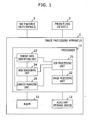
- Fig. 1 shows a block diagram that indicates a configuration of an image forming apparatus according to an embodiment of the present invention.
- the image forming apparatus shown in Fig. 1 is a printer, a multi function peripheral or the like, and includes an image processing apparatus 1, a network interface 2, and a printing device 3.
- the image processing apparatus 1 is connected to the network interface 2, the printing device 3 and the like, and performs a print job on the basis of a print request.
- the image processing apparatus 1 is configured as a computer, ASIC (Application Specific Integrated Circuit), and/or the like.
- the network interface 2 is a communication device that performs communication through a network with an unshown host device. For example, the network interface 2 receives print data described in a page description language as a print request from an unshown host device.
- the printing device 3 is provided print image data from the image processing apparatus 1, performs sorts of processes (e.g. half toning) for the print image data, and performs printing on the basis of the processed data.
- This image processing apparatus 1 include a processor 11, a RAM (Random Access Memory) 12, and an auxiliary storage device 13.
- a processor 11 a processor 11, a RAM (Random Access Memory) 12, and an auxiliary storage device 13.
- the processor 11 embodies processing units that perform sorts of processes using a CPU (Central Processing Unit), an ASIC or the like.
- the RAM 12 is a volatile storage device that temporarily stores sorts of data related to a process performed by the processor 11.
- the auxiliary storage device 13 is a non volatile storage device that has stored sorts of data and a program executed by the CPU in the processor 11.
- a ROM Read Only Memory
- flash memory a hard disc drive or the like is used as the auxiliary storage device 13.
- a job processing unit 21 an image processing unit 22, a memory area identifying unit 23, an area reassigning unit 24 and an address managing unit 25 are embodied.
- the job processing unit 21 receives a request based on a user operation to an unshown operation panel and a request such as a print request received from an unshown host device, and causes to perform a job such as a print job corresponding to the request.
- the image processing unit 22 generates image data by rasterizing PDL (Page Description Language) data or the like, and generates print image data by performing image processing (resolution conversion, enlargement/reduction, rotation and the like) for the image data and provides the print image data to the printing device 3.
- image processing resolution conversion, enlargement/reduction, rotation and the like
- the image processing unit 22 performs image processing for a print job.
- the job processing unit 21 and/or the image processing unit 22 when necessary, allocate/allocates memory areas in the RAM 12, and perform/performs the print job and/or the image processing using the allocated memory area.
- the job processing unit 21 performs a defragmentation process using the memory area identifying unit 23, the area reassigning unit 24, and the address managing unit 25.
- the memory area identifying unit 23 identifies logical memory areas in use that are required to guarantee stored data and logical memory areas not in use that are not required to guarantee stored data.
- the area reassigning unit 24 allocates one physical memory area for consecutive plural logical memory areas not in use.
- the area reassigning unit 24 rearranges one or more physical memory areas corresponding to one logical memory area in use so as to consecutively locate the aforementioned one or more physical memory areas; and in the defragmentation process, the address managing unit 25 performs address mapping between the aforementioned logical memory area in use and the rearranged one or more physical memory areas.
- the area reassigning unit 24 copies data in the aforementioned one or more physical memory areas before the rearrangement into the rearranged one or more physical memory areas.
- the area reassigning unit 24 does not copy data in physical memory areas corresponding to the consecutive plural logical memory areas not in use into the allocated physical memory area.
- the address managing unit 25 performs address conversion between a virtual address space and a physical address space on the basis of mapping data and manages the mapping data, which indicates relationship between the physical address space of the RAM 12 and the virtual address space.
- the address managing unit 21 is embodied as a memory management unit (MMU).
- the address managing unit 25 performs address mapping (i.e. renewing the mapping data) between the consecutive plural logical memory areas not in use and the aforementioned one physical memory area assigned to the consecutive plural logical memory areas not in use.
- the job processing unit 21 Upon receiving a print request through the network interface 2, the job processing unit 21 causes the image processing unit 22 to generate print image data based on the print request, and provides the print image data to the printing device 3 to perform printing. At this time, the job processing unit 21 and the image processing unit 22 allocate memory areas required for data processing in the RAM 12, and perform the data processing using the memory areas.
- fragmentation occurs in the RAM 12 and therefore the job processing unit 21 performs defragmentation at a predetermined timing.
- FIG. 2 shows a flowchart that explains a behavior of an image processing apparatus in Fig. 1 in a defragmentation process.
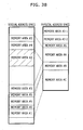
- Fig. 3A and Fig. 3B show diagrams that indicates an example of arrangement of memory areas by the image processing apparatus in Fig. 1 before and after the defragmentation process.
- Fig. 3A indicates an example of arrangement of the memory areas before the defragmentation process
- Fig. 3B indicates an example of arrangement of the memory areas after the defragmentation process.
- the memory area identifying unit 23 identifies logical memory areas in use that are required to guarantee stored data and logical memory areas not in use that are not required to guarantee stored data (in Step S1).
- a logical memory area in which image data of the print job is stored is identified as a logical memory area not in use.
- a logical memory area continuously used for management of jobs including a job that has not been processed yet is identified as a logical memory area in use.
- the logical memory areas #1 to #9 are allocated, and the physical memory areas #1 to #9 are allocated so as to correspond to the logical memory areas #1 to #9.
- the logical memory area #2 is allocated so as to correspond to the plural physical memory areas #2-1 and #2-2.
- the logical memory areas #4 and #9 are allocated so as to correspond to the plural physical memory areas #4-1 and #4-2, and #9-1 and #9-2, respectively.
- the memory area identifying unit 23 identifies physical memory areas corresponding to the identified logical memory areas in use. Specifically, the memory area identifying unit 23 identifies physical memory areas corresponding to the logical memory areas in use on the basis of the mapping data of the address managing unit 25 (in Step S2).
- the area reassigning unit 24 rearranges one or more physical memory areas corresponding to one of the identified one or more logical memory areas in use so as to consecutively locate the aforementioned one or more physical memory areas, and the address managing unit 25 performs address mapping between the aforementioned logical memory area in use and the rearranged one or more physical memory areas in the defragmentation process (in Step S3). Subsequently, the area reassigning unit 24 copies data in the aforementioned one or more physical memory areas before the rearrangement into the rearranged one or more physical memory areas.
- Step S3 Until the rearrangement is completed for all of the identified logical memory areas in use, the aforementioned process in Step S3 is performed one by one in order (in Step S4).
- Fig. 3A and Fig. 3B for example, if the logical memory area #2 and the logical memory area #6 are in use, then the physical memory areas #2-1, #2-2, and #6 corresponding to them are rearranged so as to be consecutively located from the top.
- the area reassigning unit 24 identifies whether one of the logical memory areas not in use identified by the memory area identifying unit 23 is consecutive to the next logical memory area not in use or not (in Step S5).
- the area reassigning unit 24 assigns one physical memory area to the consecutive plural logical memory areas, and the address managing unit 25 performs address mapping between the consecutive plural logical memory areas and the aforementioned one physical memory area assigned thereto (in Step S6).
- the area reassigning unit 24 assigns one physical memory area to one logical memory area
- the address managing unit 25 performs address mapping between the aforementioned one logical memory area and the aforementioned one physical memory area assigned to the aforementioned one logical memory area (in Step S7).
- the area reassigning unit 24 does not copy data in physical memory areas corresponding to the consecutive plural logical memory areas not in use into the assigned physical memory area.
- Step S8 Until the rearrangement is completed for all of the identified logical memory areas not in use, the aforementioned processes in Steps S5 to S7 are performed one by one in order (in Step S8).
- Fig. 3A and Fig. 3B for example, if the logical memory areas other than the logical memory area #2 and the logical memory area #6 are not in use, then the logical memory area #5 and the logical memory area #4 are consecutive, and therefore, one physical memory area #A is assigned to the logical memory area #5 and the logical memory area #4, and the physical memory area #A has the size equal to the sum of the size of the logical memory area #5 and the size of the logical memory area #4. After that, the logical memory area #5 and the logical memory area #4 are handled as one logical memory area.
- one physical memory area #C is assigned to the logical memory area #9, the logical memory area #8, and the logical memory area #1, and the physical memory area #C has the size equal to the sum of the size of the logical memory area #9, the logical memory area #8, and the size of the logical memory area #1.
- the logical memory area #3 is not consecutive to any other logical memory areas not in use, one physical memory area B is assigned to the logical memory area #3, and the physical memory area #B has the size equal to the size of the logical memory area #3.
- the physical memory areas #A, #B, and #C are assigned consecutively next to the physical memory areas #2-1, #2-2, and #6.
- the memory area identifying unit 23 identifies logical memory areas in use that are required to guarantee stored data and logical memory areas not in use that are not required to guarantee stored data among memory areas allocated in the RAM 12, the area reassigning unit 24 assigns one physical memory area to consecutive plural logical memory areas not in use among the logical memory areas identified by the memory area identifying unit 23, and the address managing unit 25 performs address mapping between the consecutive plural logical memory areas not in use and the aforementioned one physical memory area assigned to the consecutive plural logical memory areas not in use.
- address mapping is performed only once for the consecutive plural logical memory areas not in use and a small number of times that the address managing unit 25 performs address mapping is sufficient, and consequently defragmentation is performed in a short time.
- the present invention is applicable to an image processing apparatus and an image forming apparatus.
Landscapes
- Engineering & Computer Science (AREA)
- Physics & Mathematics (AREA)
- General Physics & Mathematics (AREA)
- Theoretical Computer Science (AREA)
- General Engineering & Computer Science (AREA)
- Microelectronics & Electronic Packaging (AREA)
- Record Information Processing For Printing (AREA)
- Image Input (AREA)
- Storing Facsimile Image Data (AREA)
- Information Retrieval, Db Structures And Fs Structures Therefor (AREA)
- Memory System Of A Hierarchy Structure (AREA)
Abstract
Description
- The present invention relates to an image processing apparatus and an image forming apparatus.
- A copier performs defragmentation of a buffer memory when image data of a predetermined number of output pages can not be consecutively stored in the buffer memory (see
PATENT LITERATURE # 1, for example). - PATENT LITERATURE #1: Japanese Patent Application Publication NO.
2007-174538 - An image processing apparatus managing a memory using a virtual memory system performs remapping between a logical memory area in a virtual address space and a physical memory area in a physical address space when performing defragmentation for the memory.
- There is a problem that if lots of fragmentation occur in a memory, remapping between a logical memory area in a virtual address space and a physical memory area in a physical address space is performed a large number of times in defragmentation, and consequently the defragmentation requires a long time. The long time required for the defragmentation causes the continuous status that a part or all of a memory area in the memory is not available continues during the long time.
- This invention has been made in view of the aforementioned problem. It is an object of the present invention to achieve an image processing apparatus and an image forming apparatus performing defragmentation in a short time.
- The present invention solves the aforementioned problem as follows.
- An image processing apparatus according to the present invention includes a memory area identifying unit that identifies logical memory areas in use that are required to guarantee stored data and logical memory areas not in use that are not required to guarantee stored data among memory areas allocated in a memory in a defragmentation process; an area reassigning unit that assigns one physical memory area to consecutive plural logical memory areas not in use among the logical memory areas identified by the memory area identifying unit in the defragmentation process; and an address managing unit that performs address mapping between the consecutive plural logical memory areas not in use and said one physical memory area assigned to the consecutive plural logical memory areas not in use.
- Therefore, address mapping is performed only once for the consecutive plural logical memory areas not in use and a small number of times of address mapping is sufficient, and consequently defragmentation is performed in a short time.
- An image forming apparatus according to the present invention includes an image processing apparatus that stores image data in a memory, performs a predetermined process for the image data, and performs a defragmentation process of the memory; and a printing device. The image processing apparatus includes a memory area identifying unit that identifies logical memory areas in use that are required to guarantee stored data and logical memory areas not in use that are not required to guarantee stored data among memory areas allocated in the memory in the defragmentation process; an area reassigning unit that assigns one physical memory area to consecutive plural logical memory areas not in use among the logical memory areas identified by the memory area identifying unit in the defragmentation process; and an address managing unit that performs address mapping between the consecutive plural logical memory areas not in use and said one physical memory area assigned to the consecutive plural logical memory areas not in use; a job processing unit that performs a print job using the printing device; and an image processing unit that performs image processing for the print job. The job processing unit and/or the image processing unit allocate/allocates the memory areas in the memory and perform/performs the print job and/or the image processing using the allocated memory area. Advantageous effect of invention
- According to the present invention, in an image processing apparatus or the like defragmentation is performed in a short time.
- These and other objects, features and advantages of the present invention will become more apparent upon reading of the following detailed description along with the accompanied drawings.
-
-
Fig. 1 shows a block diagram that indicates a configuration of an image forming apparatus according to an embodiment of the present invention; -
Fig. 2 shows a flowchart that explains a behavior of an image processing apparatus inFig. 1 in a defragmentation process; -
Fig. 3A shows a diagram that indicates an example of arrangement of memory areas by the image processing apparatus inFig. 1 before the defragmentation process; and -
Fig. 3B shows a diagram that indicates an example of arrangement of memory areas by the image processing apparatus inFig. 1 after the defragmentation process. - Hereinafter, an embodiment according to aspects of the present invention will be explained with reference to drawings.
-
Fig. 1 shows a block diagram that indicates a configuration of an image forming apparatus according to an embodiment of the present invention. The image forming apparatus shown inFig. 1 is a printer, a multi function peripheral or the like, and includes animage processing apparatus 1, anetwork interface 2, and aprinting device 3. - The
image processing apparatus 1 is connected to thenetwork interface 2, theprinting device 3 and the like, and performs a print job on the basis of a print request. Theimage processing apparatus 1 is configured as a computer, ASIC (Application Specific Integrated Circuit), and/or the like. Thenetwork interface 2 is a communication device that performs communication through a network with an unshown host device. For example, thenetwork interface 2 receives print data described in a page description language as a print request from an unshown host device. Theprinting device 3 is provided print image data from theimage processing apparatus 1, performs sorts of processes (e.g. half toning) for the print image data, and performs printing on the basis of the processed data. - This
image processing apparatus 1 include aprocessor 11, a RAM (Random Access Memory) 12, and anauxiliary storage device 13. - The
processor 11 embodies processing units that perform sorts of processes using a CPU (Central Processing Unit), an ASIC or the like. TheRAM 12 is a volatile storage device that temporarily stores sorts of data related to a process performed by theprocessor 11. Theauxiliary storage device 13 is a non volatile storage device that has stored sorts of data and a program executed by the CPU in theprocessor 11. As theauxiliary storage device 13, a ROM (Read Only Memory), a flash memory, a hard disc drive or the like is used. - In the
processor 11, ajob processing unit 21, animage processing unit 22, a memoryarea identifying unit 23, anarea reassigning unit 24 and anaddress managing unit 25 are embodied. - The
job processing unit 21 receives a request based on a user operation to an unshown operation panel and a request such as a print request received from an unshown host device, and causes to perform a job such as a print job corresponding to the request. - The
image processing unit 22 generates image data by rasterizing PDL (Page Description Language) data or the like, and generates print image data by performing image processing (resolution conversion, enlargement/reduction, rotation and the like) for the image data and provides the print image data to theprinting device 3.
Thus, theimage processing unit 22 performs image processing for a print job. - The
job processing unit 21 and/or theimage processing unit 22, when necessary, allocate/allocates memory areas in theRAM 12, and perform/performs the print job and/or the image processing using the allocated memory area. - Further, at a timing when the
job processing unit 21 completes a print job or the like, thejob processing unit 21 performs a defragmentation process using the memoryarea identifying unit 23, thearea reassigning unit 24, and theaddress managing unit 25. - In the defragmentation process, among memory areas allocated in the
RAM 12, the memoryarea identifying unit 23 identifies logical memory areas in use that are required to guarantee stored data and logical memory areas not in use that are not required to guarantee stored data. - In the defragmentation process, among the logical memory areas identified by the memory area identifying unit, the
area reassigning unit 24 allocates one physical memory area for consecutive plural logical memory areas not in use. - In this embodiment; in the defragmentation process, the
area reassigning unit 24 rearranges one or more physical memory areas corresponding to one logical memory area in use so as to consecutively locate the aforementioned one or more physical memory areas; and in the defragmentation process, theaddress managing unit 25 performs address mapping between the aforementioned logical memory area in use and the rearranged one or more physical memory areas. - In this embodiment, the
area reassigning unit 24 copies data in the aforementioned one or more physical memory areas before the rearrangement into the rearranged one or more physical memory areas. On the other hand, for the logical memory areas not in use, thearea reassigning unit 24 does not copy data in physical memory areas corresponding to the consecutive plural logical memory areas not in use into the allocated physical memory area. - The
address managing unit 25 performs address conversion between a virtual address space and a physical address space on the basis of mapping data and manages the mapping data, which indicates relationship between the physical address space of theRAM 12 and the virtual address space. For example, theaddress managing unit 21 is embodied as a memory management unit (MMU). - In the defragmentation process, the
address managing unit 25 performs address mapping (i.e. renewing the mapping data) between the consecutive plural logical memory areas not in use and the aforementioned one physical memory area assigned to the consecutive plural logical memory areas not in use. - The following part explains a behavior of the aforementioned image forming apparatus.
- Upon receiving a print request through the
network interface 2, thejob processing unit 21 causes theimage processing unit 22 to generate print image data based on the print request, and provides the print image data to theprinting device 3 to perform printing. At this time, thejob processing unit 21 and theimage processing unit 22 allocate memory areas required for data processing in theRAM 12, and perform the data processing using the memory areas. - Due to dynamically allocating the memory areas, fragmentation occurs in the
RAM 12 and therefore thejob processing unit 21 performs defragmentation at a predetermined timing. - Here the defragmentation process by the
image processing apparatus 1 is explained.Fig. 2 shows a flowchart that explains a behavior of an image processing apparatus inFig. 1 in a defragmentation process.Fig. 3A andFig. 3B show diagrams that indicates an example of arrangement of memory areas by the image processing apparatus inFig. 1 before and after the defragmentation process.Fig. 3A indicates an example of arrangement of the memory areas before the defragmentation process, andFig. 3B indicates an example of arrangement of the memory areas after the defragmentation process. - Firstly, among memory areas allocated in the
RAM 12 by thejob processing unit 21, theimage processing unit 22 and the like, the memoryarea identifying unit 23 identifies logical memory areas in use that are required to guarantee stored data and logical memory areas not in use that are not required to guarantee stored data (in Step S1). - For example, at a timing after completion of a print job, a logical memory area in which image data of the print job is stored is identified as a logical memory area not in use. Further, a logical memory area continuously used for management of jobs including a job that has not been processed yet is identified as a logical memory area in use.
- In
Fig. 3A , the logicalmemory areas # 1 to #9 are allocated, and the physicalmemory areas # 1 to #9 are allocated so as to correspond to the logicalmemory areas # 1 to #9. However, the logicalmemory area # 2 is allocated so as to correspond to the plural physical memory areas #2-1 and #2-2. In the same manner, the logicalmemory areas # 4 and #9 are allocated so as to correspond to the plural physical memory areas #4-1 and #4-2, and #9-1 and #9-2, respectively. - Subsequently, the memory
area identifying unit 23 identifies physical memory areas corresponding to the identified logical memory areas in use. Specifically, the memoryarea identifying unit 23 identifies physical memory areas corresponding to the logical memory areas in use on the basis of the mapping data of the address managing unit 25 (in Step S2). - The
area reassigning unit 24 rearranges one or more physical memory areas corresponding to one of the identified one or more logical memory areas in use so as to consecutively locate the aforementioned one or more physical memory areas, and theaddress managing unit 25 performs address mapping between the aforementioned logical memory area in use and the rearranged one or more physical memory areas in the defragmentation process (in Step S3). Subsequently, thearea reassigning unit 24 copies data in the aforementioned one or more physical memory areas before the rearrangement into the rearranged one or more physical memory areas. - Until the rearrangement is completed for all of the identified logical memory areas in use, the aforementioned process in Step S3 is performed one by one in order (in Step S4).
- In
Fig. 3A andFig. 3B , for example, if the logicalmemory area # 2 and the logicalmemory area # 6 are in use, then the physical memory areas #2-1, #2-2, and #6 corresponding to them are rearranged so as to be consecutively located from the top. - Upon completing the rearrangement for all of the identified logical memory areas in use, the
area reassigning unit 24 identifies whether one of the logical memory areas not in use identified by the memoryarea identifying unit 23 is consecutive to the next logical memory area not in use or not (in Step S5). - If the logical memory areas not in use are consecutive, the
area reassigning unit 24 assigns one physical memory area to the consecutive plural logical memory areas, and theaddress managing unit 25 performs address mapping between the consecutive plural logical memory areas and the aforementioned one physical memory area assigned thereto (in Step S6). - Contrarily, if the logical memory areas not in use are not consecutive, the
area reassigning unit 24 assigns one physical memory area to one logical memory area, and theaddress managing unit 25 performs address mapping between the aforementioned one logical memory area and the aforementioned one physical memory area assigned to the aforementioned one logical memory area (in Step S7). - For the logical memory areas not in use, the
area reassigning unit 24 does not copy data in physical memory areas corresponding to the consecutive plural logical memory areas not in use into the assigned physical memory area. - Until the rearrangement is completed for all of the identified logical memory areas not in use, the aforementioned processes in Steps S5 to S7 are performed one by one in order (in Step S8).
- In
Fig. 3A andFig. 3B , for example, if the logical memory areas other than the logicalmemory area # 2 and the logicalmemory area # 6 are not in use, then the logicalmemory area # 5 and the logicalmemory area # 4 are consecutive, and therefore, one physical memory area #A is assigned to the logicalmemory area # 5 and the logicalmemory area # 4, and the physical memory area #A has the size equal to the sum of the size of the logicalmemory area # 5 and the size of the logicalmemory area # 4. After that, the logicalmemory area # 5 and the logicalmemory area # 4 are handled as one logical memory area. - In the same manner, since the logical
memory area # 9, the logicalmemory area # 8, and the logicalmemory area # 1 are consecutive, one physical memory area #C is assigned to the logicalmemory area # 9, the logicalmemory area # 8, and the logicalmemory area # 1, and the physical memory area #C has the size equal to the sum of the size of the logicalmemory area # 9, the logicalmemory area # 8, and the size of the logicalmemory area # 1. - Contrarily, since the logical
memory area # 3 is not consecutive to any other logical memory areas not in use, one physical memory area B is assigned to the logicalmemory area # 3, and the physical memory area #B has the size equal to the size of the logicalmemory area # 3. - Thus, the physical memory areas #A, #B, and #C are assigned consecutively next to the physical memory areas #2-1, #2-2, and #6.
- As mentioned, in the aforementioned embodiment, in a defragmentation process, the memory
area identifying unit 23 identifies logical memory areas in use that are required to guarantee stored data and logical memory areas not in use that are not required to guarantee stored data among memory areas allocated in theRAM 12, thearea reassigning unit 24 assigns one physical memory area to consecutive plural logical memory areas not in use among the logical memory areas identified by the memoryarea identifying unit 23, and theaddress managing unit 25 performs address mapping between the consecutive plural logical memory areas not in use and the aforementioned one physical memory area assigned to the consecutive plural logical memory areas not in use. - Therefore, address mapping is performed only once for the consecutive plural logical memory areas not in use and a small number of times that the
address managing unit 25 performs address mapping is sufficient, and consequently defragmentation is performed in a short time. - It should be noted that the aforementioned description has been presented for purposes of illustration and description, and is not intended to be exhaustive nor to limit the present invention.
- Further, it should be understood that various changes and modifications to the embodiments described herein will be apparent to those skilled in the art. Such changes and modifications may be made without departing from the spirit and scope of the present subject matter and without diminishing its intended advantages. It is therefore intended that such changes and modifications be covered by the appended claims.
- For example, the present invention is applicable to an image processing apparatus and an image forming apparatus.
Claims (6)
- An image processing apparatus that stores image data in a memory, performs a predetermined process for the image data, and performs a defragmentation process of the memory, comprising:a memory area identifying unit that identifies logical memory areas in use that are required to guarantee stored data and logical memory areas not in use that are not required to guarantee stored data among memory areas allocated in the memory in the defragmentation process;an area reassigning unit that assigns one physical memory area to consecutive plural logical memory areas not in use among the logical memory areas identified by the memory area identifying unit in the defragmentation process; andan address managing unit that performs address mapping between the consecutive plural logical memory areas not in use and said one physical memory area assigned to the consecutive plural logical memory areas not in use in the defragmentation process.
- The image processing apparatus according to claim 1, wherein:the area reassigning unit rearranges one or more physical memory areas corresponding to one of the logical memory areas in use so as to consecutively locate said one or more physical memory areas in the defragmentation process; andthe address managing unit performs address mapping between said logical memory area in use and the rearranged one or more physical memory areas in the defragmentation process.
- The image processing apparatus according to claim 2, wherein the area reassigning unit copies data in said one or more physical memory areas before the rearrangement into the rearranged one or more physical memory areas.
- The image processing apparatus according to claim 1, wherein for the logical memory areas not in use, the area reassigning unit does not copy data in physical memory areas corresponding to the consecutive plural logical memory areas not in use into the assigned physical memory area.
- An image forming apparatus, comprising: an image processing apparatus that stores image data in a memory, performs a predetermined process for the image data, and performs a defragmentation process of the memory; and a printing device;
wherein the image processing apparatus comprises:a memory area identifying unit that identifies logical memory areas in use that are required to guarantee stored data and logical memory areas not in use that are not required to guarantee stored data among memory areas allocated in the memory in the defragmentation process;an area reassigning unit that assigns one physical memory area to consecutive plural logical memory areas not in use among the logical memory areas identified by the memory area identifying unit in the defragmentation process; andan address managing unit that performs address mapping between the consecutive plural logical memory areas not in use and said one physical memory area assigned to the consecutive plural logical memory areas not in use;a job processing unit that performs a print job using the printing device; andan image processing unit that performs image processing for the print job;wherein the job processing unit and/or the image processing unit allocate/allocates the memory areas in the memory and perform/performs the print job and/or the image processing using the allocated memory area. - The image forming apparatus according to claim 5, wherein the image processing apparatus performs the defragmentation process before the job processing unit completes the print job.
Applications Claiming Priority (2)
| Application Number | Priority Date | Filing Date | Title |
|---|---|---|---|
| JP2012001870 | 2012-01-10 | ||
| PCT/JP2012/083447 WO2013105428A1 (en) | 2012-01-10 | 2012-12-25 | Image processing apparatus and image forming apparatus |
Publications (2)
| Publication Number | Publication Date |
|---|---|
| EP2804368A1 true EP2804368A1 (en) | 2014-11-19 |
| EP2804368A4 EP2804368A4 (en) | 2015-09-23 |
Family
ID=48781386
Family Applications (1)
| Application Number | Title | Priority Date | Filing Date |
|---|---|---|---|
| EP12865270.8A Withdrawn EP2804368A4 (en) | 2012-01-10 | 2012-12-25 | IMAGE PROCESSING APPARATUS AND IMAGE FORMING APPARATUS |
Country Status (5)
| Country | Link |
|---|---|
| US (1) | US20150015913A1 (en) |
| EP (1) | EP2804368A4 (en) |
| JP (1) | JP5832556B2 (en) |
| CN (1) | CN104170364B (en) |
| WO (1) | WO2013105428A1 (en) |
Cited By (1)
| Publication number | Priority date | Publication date | Assignee | Title |
|---|---|---|---|---|
| IT201800002644A1 (en) * | 2018-02-13 | 2019-08-13 | St Microelectronics Srl | PROCEDURE FOR HANDLING INTEGRATED CIRCUIT CARDS, CORRESPONDING CARD AND EQUIPMENT |
Families Citing this family (6)
| Publication number | Priority date | Publication date | Assignee | Title |
|---|---|---|---|---|
| JP2551225Y2 (en) | 1990-11-29 | 1997-10-22 | 株式会社ケンウッド | Diaphragm paper machine |
| CN110162483B (en) * | 2018-02-12 | 2020-10-20 | 上海寒武纪信息科技有限公司 | Static memory defragmentation method, device, computer equipment and storage medium |
| CN109664620B (en) * | 2018-12-07 | 2020-03-13 | 森大(深圳)技术有限公司 | Print data processing method, device and equipment |
| US11972034B1 (en) | 2020-10-29 | 2024-04-30 | Amazon Technologies, Inc. | Hardware-assisted obscuring of cache access patterns |
| US12229248B1 (en) * | 2021-03-16 | 2025-02-18 | Amazon Technologies, Inc. | Obscuring memory access patterns through page remapping |
| US11755496B1 (en) | 2021-12-10 | 2023-09-12 | Amazon Technologies, Inc. | Memory de-duplication using physical memory aliases |
Family Cites Families (30)
| Publication number | Priority date | Publication date | Assignee | Title |
|---|---|---|---|---|
| US5797689A (en) * | 1996-01-24 | 1998-08-25 | Hewlett-Packard Company | Avoiding memory fragmentation in printers |
| GB9606927D0 (en) * | 1996-04-02 | 1996-06-05 | Memory Corp Plc | Data storage devices |
| US5720015A (en) * | 1996-04-22 | 1998-02-17 | Lexmark International, Inc. | Method and apparatus for providing remote printer resource management |
| US6038033A (en) * | 1997-08-20 | 2000-03-14 | Lexmark International, Inc. | Method and apparatus for compressing and decompressing print data in the background operations of a printer |
| US6938245B1 (en) * | 1997-10-29 | 2005-08-30 | Veritas Operating Corporation | Interactive debugging system with debug data base system |
| US6038636A (en) * | 1998-04-27 | 2000-03-14 | Lexmark International, Inc. | Method and apparatus for reclaiming and defragmenting a flash memory device |
| US6668304B1 (en) * | 2000-01-18 | 2003-12-23 | International Business Machines Corporation | Transaction support on logical disks |
| PL354638A1 (en) * | 2002-06-20 | 2003-12-29 | Advanced Digital Broadcast Ltd.Advanced Digital Broadcast Ltd. | Method of memory allocation for images |
| US7181587B1 (en) * | 2003-08-18 | 2007-02-20 | Cray Inc. | Mapping an arbitrary number of contiguous memory pages at an arbitrary alignment |
| JP2006113648A (en) * | 2004-10-12 | 2006-04-27 | Hitachi Ltd | Disk array device |
| JP2006293543A (en) * | 2005-04-07 | 2006-10-26 | Nec Corp | Storage system and dynamic recovery method of physical storage region |
| GB2426360A (en) * | 2005-05-18 | 2006-11-22 | Symbian Software Ltd | Reorganisation of memory for conserving power in a computing device |
| US7809777B2 (en) * | 2005-07-01 | 2010-10-05 | Qnx Software Systems Gmbh & Co. Kg | File system having deferred verification of data integrity |
| US8959125B2 (en) * | 2005-07-01 | 2015-02-17 | 226008 Ontario Inc. | File system having inverted hierarchical structure |
| US7873683B2 (en) * | 2005-07-01 | 2011-01-18 | Qnx Software Systems Gmbh & Co. Kg | File system having transaction record coalescing |
| US20070005874A1 (en) * | 2005-07-01 | 2007-01-04 | Dan Dodge | File system storing transaction records in flash-like media |
| JP2007174538A (en) | 2005-12-26 | 2007-07-05 | Konica Minolta Business Technologies Inc | Image forming apparatus and image forming method |
| US20070180187A1 (en) * | 2006-02-01 | 2007-08-02 | Keith Olson | Reducing power consumption by disabling refresh of unused portions of DRAM during periods of device inactivity |
| JP4993928B2 (en) * | 2006-03-23 | 2012-08-08 | 株式会社日立製作所 | Storage system, storage area release method, and storage system |
| JP4533968B2 (en) * | 2007-12-28 | 2010-09-01 | 株式会社東芝 | Semiconductor memory device, control method therefor, controller, information processing device |
| US8782371B2 (en) * | 2008-03-31 | 2014-07-15 | Konica Minolta Laboratory U.S.A., Inc. | Systems and methods for memory management for rasterization |
| KR101606453B1 (en) * | 2009-05-13 | 2016-04-01 | 삼성전자주식회사 | Method of read/write performance of non-volatile data storage device |
| US8856438B1 (en) * | 2011-12-09 | 2014-10-07 | Western Digital Technologies, Inc. | Disk drive with reduced-size translation table |
| TWI423022B (en) * | 2011-02-15 | 2014-01-11 | Phison Electronics Corp | Memory management method, memory controller and memory storage apparatus |
| TWI438630B (en) * | 2011-03-22 | 2014-05-21 | Phison Electronics Corp | Data merging method for non-volatile memory and controller and stoarge apparatus using the same |
| TWI454911B (en) * | 2011-10-12 | 2014-10-01 | Phison Electronics Corp | Data writing method, memory controller and memory storage apparatus |
| CN103064723B (en) * | 2011-10-18 | 2016-01-20 | 财团法人工业技术研究院 | Method and computer system for identifying virtual machine memory |
| TWI540428B (en) * | 2011-11-18 | 2016-07-01 | 群聯電子股份有限公司 | Data writing method, memory controller and memory storage apparatus |
| US9298460B2 (en) * | 2011-11-29 | 2016-03-29 | International Business Machines Corporation | Register management in an extended processor architecture |
| JP5041105B1 (en) * | 2012-03-23 | 2012-10-03 | 富士ゼロックス株式会社 | Spool control device and program |
-
2012
- 2012-12-25 JP JP2013553240A patent/JP5832556B2/en not_active Expired - Fee Related
- 2012-12-25 EP EP12865270.8A patent/EP2804368A4/en not_active Withdrawn
- 2012-12-25 WO PCT/JP2012/083447 patent/WO2013105428A1/en not_active Ceased
- 2012-12-25 CN CN201280070652.1A patent/CN104170364B/en not_active Expired - Fee Related
- 2012-12-25 US US14/368,930 patent/US20150015913A1/en not_active Abandoned
Cited By (4)
| Publication number | Priority date | Publication date | Assignee | Title |
|---|---|---|---|---|
| IT201800002644A1 (en) * | 2018-02-13 | 2019-08-13 | St Microelectronics Srl | PROCEDURE FOR HANDLING INTEGRATED CIRCUIT CARDS, CORRESPONDING CARD AND EQUIPMENT |
| EP3525500A1 (en) * | 2018-02-13 | 2019-08-14 | STMicroelectronics Srl | Method for reducing non-volatile memory fragmentation in integrated circuit cards, corresponding card and apparatus |
| US11481133B2 (en) | 2018-02-13 | 2022-10-25 | Stmicroelectronics S.R.L. | Method of managing integrated circuits cards by widening the biggest empty region, corresponding card and apparatus |
| US11995333B2 (en) | 2018-02-13 | 2024-05-28 | Stmicroelectronics S.R.L. | Method for reducing non-volatile memory fragmentation in integrated circuit cards, corresponding card and apparatus |
Also Published As
| Publication number | Publication date |
|---|---|
| EP2804368A4 (en) | 2015-09-23 |
| US20150015913A1 (en) | 2015-01-15 |
| WO2013105428A1 (en) | 2013-07-18 |
| JPWO2013105428A1 (en) | 2015-05-11 |
| JP5832556B2 (en) | 2015-12-16 |
| CN104170364B (en) | 2017-03-15 |
| CN104170364A (en) | 2014-11-26 |
Similar Documents
| Publication | Publication Date | Title |
|---|---|---|
| US20150015913A1 (en) | Image processing apparatus and image forming apparatus | |
| CN102402404B (en) | Print controlling apparatus, print system and print control program | |
| US9146698B2 (en) | Print management apparatus, non-transitory computer readable medium, and printing system | |
| JP5482528B2 (en) | Printed document conversion apparatus and program | |
| US20150134892A1 (en) | Information processing apparatus, method of controlling the same, and storage medium | |
| US7911639B2 (en) | Image forming device | |
| US9552170B2 (en) | Memory managing apparatus and image processing apparatus | |
| US8928914B2 (en) | Image processing apparatus, information processing method, and storage medium | |
| US20140359205A1 (en) | Mounting method in an electronic apparatus | |
| JP5471681B2 (en) | Image processing apparatus and image processing program | |
| JP2010120376A (en) | System and method for frame buffer management | |
| US7484070B1 (en) | Selective memory block remapping | |
| US9047552B2 (en) | Forming system and image forming apparatus that generate image log data to server | |
| US9769331B2 (en) | Image forming apparatus with improved memory allocation to minimize delay in processing images | |
| JP5750018B2 (en) | Image processing system, printing system, control device, image processing method and program | |
| US11461224B2 (en) | System and method for reducing memory fragmentation in a device lacking graphics memory management unit | |
| US9179037B2 (en) | Image forming apparatus, controlling device and non-transitory computer readable medium for providing an available storage space | |
| JP6078954B2 (en) | Image processing device | |
| JP2011221785A (en) | Information processor, memory management method and program | |
| JP6372705B2 (en) | Image forming apparatus | |
| JP2018032148A (en) | Print control device, print control method and program | |
| JP5787211B2 (en) | Image processing apparatus and image processing program | |
| JP2016155280A (en) | Control device, control method and program | |
| JP2006163913A (en) | Printing system | |
| KR20050072224A (en) | Image forming apparatus and the method of memory management thereof |
Legal Events
| Date | Code | Title | Description |
|---|---|---|---|
| PUAI | Public reference made under article 153(3) epc to a published international application that has entered the european phase |
Free format text: ORIGINAL CODE: 0009012 |
|
| 17P | Request for examination filed |
Effective date: 20140729 |
|
| AK | Designated contracting states |
Kind code of ref document: A1 Designated state(s): AL AT BE BG CH CY CZ DE DK EE ES FI FR GB GR HR HU IE IS IT LI LT LU LV MC MK MT NL NO PL PT RO RS SE SI SK SM TR |
|
| DAX | Request for extension of the european patent (deleted) | ||
| RA4 | Supplementary search report drawn up and despatched (corrected) |
Effective date: 20150824 |
|
| RIC1 | Information provided on ipc code assigned before grant |
Ipc: G06K 15/02 20060101ALI20150818BHEP Ipc: G06F 12/00 20060101ALI20150818BHEP Ipc: G06F 12/10 20060101ALI20150818BHEP Ipc: G06F 12/08 20060101ALI20150818BHEP Ipc: B41J 5/30 20060101ALI20150818BHEP Ipc: G06F 12/02 20060101ALI20150818BHEP Ipc: H04N 1/21 20060101AFI20150818BHEP |
|
| 17Q | First examination report despatched |
Effective date: 20160607 |
|
| STAA | Information on the status of an ep patent application or granted ep patent |
Free format text: STATUS: THE APPLICATION IS DEEMED TO BE WITHDRAWN |
|
| 18D | Application deemed to be withdrawn |
Effective date: 20170301 |