EP2800203A1 - Antenna arrangement - Google Patents
Antenna arrangement Download PDFInfo
- Publication number
- EP2800203A1 EP2800203A1 EP14158214.8A EP14158214A EP2800203A1 EP 2800203 A1 EP2800203 A1 EP 2800203A1 EP 14158214 A EP14158214 A EP 14158214A EP 2800203 A1 EP2800203 A1 EP 2800203A1
- Authority
- EP
- European Patent Office
- Prior art keywords
- antenna
- antenna element
- circuit board
- printed circuit
- ground plane
- Prior art date
- Legal status (The legal status is an assumption and is not a legal conclusion. Google has not performed a legal analysis and makes no representation as to the accuracy of the status listed.)
- Withdrawn
Links
- 239000002184 metal Substances 0.000 claims abstract description 12
- 238000002955 isolation Methods 0.000 claims description 14
- 239000004020 conductor Substances 0.000 claims description 7
- 229910000679 solder Inorganic materials 0.000 claims description 2
- PEZNEXFPRSOYPL-UHFFFAOYSA-N (bis(trifluoroacetoxy)iodo)benzene Chemical compound FC(F)(F)C(=O)OI(OC(=O)C(F)(F)F)C1=CC=CC=C1 PEZNEXFPRSOYPL-UHFFFAOYSA-N 0.000 abstract description 9
- 238000000034 method Methods 0.000 description 8
- 230000005404 monopole Effects 0.000 description 5
- 230000008569 process Effects 0.000 description 5
- 238000010276 construction Methods 0.000 description 4
- 238000005516 engineering process Methods 0.000 description 4
- 230000005284 excitation Effects 0.000 description 3
- 239000007769 metal material Substances 0.000 description 3
- 238000005452 bending Methods 0.000 description 2
- 230000005684 electric field Effects 0.000 description 2
- 238000004080 punching Methods 0.000 description 2
- 230000008859 change Effects 0.000 description 1
- 238000005352 clarification Methods 0.000 description 1
- 239000003989 dielectric material Substances 0.000 description 1
- 230000009977 dual effect Effects 0.000 description 1
- 238000001914 filtration Methods 0.000 description 1
- 238000010348 incorporation Methods 0.000 description 1
- 238000004519 manufacturing process Methods 0.000 description 1
- 238000004806 packaging method and process Methods 0.000 description 1
- 230000009467 reduction Effects 0.000 description 1
- 230000000717 retained effect Effects 0.000 description 1
- 230000007306 turnover Effects 0.000 description 1
Images

Classifications
-
- H—ELECTRICITY
- H01—ELECTRIC ELEMENTS
- H01Q—ANTENNAS, i.e. RADIO AERIALS
- H01Q9/00—Electrically-short antennas having dimensions not more than twice the operating wavelength and consisting of conductive active radiating elements
- H01Q9/04—Resonant antennas
- H01Q9/0407—Substantially flat resonant element parallel to ground plane, e.g. patch antenna
- H01Q9/045—Substantially flat resonant element parallel to ground plane, e.g. patch antenna with particular feeding means
-
- H—ELECTRICITY
- H01—ELECTRIC ELEMENTS
- H01Q—ANTENNAS, i.e. RADIO AERIALS
- H01Q1/00—Details of, or arrangements associated with, antennas
- H01Q1/12—Supports; Mounting means
- H01Q1/22—Supports; Mounting means by structural association with other equipment or articles
- H01Q1/24—Supports; Mounting means by structural association with other equipment or articles with receiving set
- H01Q1/241—Supports; Mounting means by structural association with other equipment or articles with receiving set used in mobile communications, e.g. GSM
- H01Q1/242—Supports; Mounting means by structural association with other equipment or articles with receiving set used in mobile communications, e.g. GSM specially adapted for hand-held use
- H01Q1/243—Supports; Mounting means by structural association with other equipment or articles with receiving set used in mobile communications, e.g. GSM specially adapted for hand-held use with built-in antennas
-
- H—ELECTRICITY
- H01—ELECTRIC ELEMENTS
- H01Q—ANTENNAS, i.e. RADIO AERIALS
- H01Q5/00—Arrangements for simultaneous operation of antennas on two or more different wavebands, e.g. dual-band or multi-band arrangements
- H01Q5/30—Arrangements for providing operation on different wavebands
- H01Q5/307—Individual or coupled radiating elements, each element being fed in an unspecified way
-
- H—ELECTRICITY
- H01—ELECTRIC ELEMENTS
- H01Q—ANTENNAS, i.e. RADIO AERIALS
- H01Q5/00—Arrangements for simultaneous operation of antennas on two or more different wavebands, e.g. dual-band or multi-band arrangements
- H01Q5/30—Arrangements for providing operation on different wavebands
- H01Q5/307—Individual or coupled radiating elements, each element being fed in an unspecified way
- H01Q5/342—Individual or coupled radiating elements, each element being fed in an unspecified way for different propagation modes
- H01Q5/357—Individual or coupled radiating elements, each element being fed in an unspecified way for different propagation modes using a single feed point
-
- H—ELECTRICITY
- H01—ELECTRIC ELEMENTS
- H01Q—ANTENNAS, i.e. RADIO AERIALS
- H01Q9/00—Electrically-short antennas having dimensions not more than twice the operating wavelength and consisting of conductive active radiating elements
- H01Q9/04—Resonant antennas
- H01Q9/0407—Substantially flat resonant element parallel to ground plane, e.g. patch antenna
-
- H—ELECTRICITY
- H01—ELECTRIC ELEMENTS
- H01Q—ANTENNAS, i.e. RADIO AERIALS
- H01Q9/00—Electrically-short antennas having dimensions not more than twice the operating wavelength and consisting of conductive active radiating elements
- H01Q9/04—Resonant antennas
- H01Q9/0407—Substantially flat resonant element parallel to ground plane, e.g. patch antenna
- H01Q9/0421—Substantially flat resonant element parallel to ground plane, e.g. patch antenna with a shorting wall or a shorting pin at one end of the element
Definitions
- the present invention solves the above problem with a device according to claim 1.
Landscapes
- Engineering & Computer Science (AREA)
- Computer Networks & Wireless Communication (AREA)
- Waveguide Aerials (AREA)
Abstract
The present invention provides a solution to how an antenna of the Patch or PIFA type can be made from a sheet metal in order for thereafter to be mounted on a printed circuit board with particularly formed mounting areas in order to provide both an inexpensive but yet robust and efficient antenna solution.
Description
- The present invention concerns an antenna arrangement comprising a printed circuit board and an antenna element mounted thereon.
- Antennas for incorporation in radio equipment entails a plurality of demands that often are difficult to combine in one product. They should be robust and, at the same time, the one and the same antenna should be able to be used with several different products; they should be mountable in a normal surface mounting process and have a low cost.
- The antennas that usually are able to handle demands on robustness the best and can be used with a plurality of different products are antennas that are placed above a ground plane and are often called Patch or PIFA antennas (Planar Inverted F Antenna). These antennas need a point of connection to connect a radio signal to the antenna, however, in most cases two points of connection are used, one for a radio signal and another for the ground plane. These two points of connection are usually placed near to each other to create an antenna with an impedance of 50 Ohms.
- There are also antennas that are located outside ground planes, they are called monopole antennas. The monopole interacts in another way with the rest of the product what makes these antennas less robust and they need to be adapted to the product to a higher extent. Most commonly, the performance is also somewhat lower than for Patch and PIFA antennas.
- There are monopole antennas that are formed in sheet metal that is punched and bent, where they are placed outside a ground plane according to
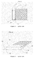
figure 1 and 2 . Theantenna element 12 is placed on thesurface 11 that lacks electrically conducting material, wherepin 13 for a radio signal is connected to the antenna element, that also can have anadditional support pin 15. It could also be considered to haveground 10 connected to theantenna element 12 via thepin 14. - With a construction according to
figure 1 and 2 , the antenna becomes a monopole type antenna and will be less robust than an antenna of the PIFA type, which has a ground plane located under the antenna element. - If there is a ground plane below the antenna, the
additional support pins 15 can not be used for mechanical support, for such a support then, only the pins for a radio signal and possibly ground, if desired, can be connected. Since these are placed near to each other, the antenna is rendered mechanically unstable. To have a stable antenna, the antenna element, which may comprise a thin, flat, electrically conductive material, usually is placed on aplastic carrier 16 according tofigure 3 . With flat is meant for instance a sheet metal of suitable thickness to enable forming for instance support pins and any slits as well as to achieve a sufficient mechanical stability. - This entails the drawback that an additional component is added and therefore an additional process step, which makes the antenna more expensive.
- There are antennas today that are formed in sheet metal for surface mounting. They are of the monopole type and are mounted outside the ground plane.
- These antennas are often not able to handle the demands on robustness since their resonance frequency most commonly change markedly when the same antenna is mounted in different products.
- Additionally, it is desirable to have a ground plane that is as large as possible to efficiently use the available area of the printed circuit board for electronics components. If the antenna can have a ground plane below itself, electronics components can be placed on the opposite side and also on the same side but below the antenna element.
- It is an object of the present invention to propose a solution or a reduction of the problems with the prior art.
- Thus, a main object is to solve the problem with how an antenna arrangement with an antenna element can be produced with a stable mechanical construction that is not unstable and can turn over, and which still provides an antenna arrangement with good performance even when the antenna arrangement is achieved by the mounting of the antenna element on a plurality of different products, such that a production of punching tools specific for a product is avoided.
- The present invention solves the above problem with a device according to claim 1.
- In this way, an antenna arrangement is provided with an antenna element and an underlying printed circuit board with a ground plane, combined with the fact that the support pins of the antenna element can be placed at a distance from each other that allows for a stiff mechanical connection between the antenna element and the printed circuit board.
- The combination of the antenna element with an underlying ground plane provides the antenna arrangement with stable radio properties, such as with Patch or PIFA antennas.
- Further, a support pin can be placed at an optional location under the antenna element for mechanical stability, since the solution with an isolation distance between the contact surface of the support pin on the printed circuit board and other metal on the printed circuit board lessens the impact from this pin on the radio properties of the antenna arrangement.
- In this way, an antenna arrangement is provided with the advantages of stable/robust radio properties corresponding to a PIFA or a Patch antenna combined with a construction that is mechanically stable without the need of a plastic carrier, that is traditionally associated with such PIFA or Patch antennas.
- Thus, such a plastic carrier can be avoided at the same time as the contact surface(s) with an isolation distance to other metal on the printed circuit board does not create any extra costs. All in all, the present invention consequently provides a cheaper product with performance similar to PIFA/Patch antennas.
-
- 1: Prior art with antenna outside ground plane, view from above
- 2: Prior art with antenna outside ground plane, view side-faced
- 3: Prior art with antenna above ground plane with isolation component
- 4: Technology according to the present invention with extra support pin with solder to surface on printed circuit board which has an isolation distance to metal, view side-faced
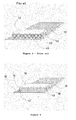
- 5: Technology according to the present invention with image of an alternative embodiment of the printed circuit board.
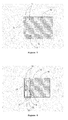
- 6: Technology according to the present invention with alternative embodiment of the antenna element with slit
- 7: Technology according to the present invention with embodiment where an antenna element protrudes partly outside the printed circuit board.
- In order to create a robust antenna element that can be mounted on a printed circuit board, the antenna element shall be placed at a distance above the ground plane of the printed circuit board.
- In order to be mechanically stable, at least two but in practice three or more pins to mount the antenna element with are needed.
- In order to achieve an inexpensive product, it is most suitable that the antenna element and connection pins are formed in one and the same component, which most suitably is a piece of flat, electrically conductive material, which is solderable in a normal surface mounting process.
- The process that in most cases is the least expensive to create a suitable design is to punch and bend a thin piece of sheet metal. The design is determined from the demands on resonance frequency, bandwidth and efficiency that the wireless system imposes.
- An antenna element of the PIFA type shall also be placed at a suitable hight above the ground plane to have good radiating properties. This can easily be created in the punching and bending process with bent pins that also have feet of appropriate size and design for the surface mounting process.
- Thereafter the antenna element may be placed in Tape and Reel, which is the name of a desired packaging for surface mounting machinery.
-
Figure 4 discloses an example of an antenna according to the present invention comprising a printed circuit board with an electrically conductingarea 10, anantenna element 12 with at least two but usuallymore pins 15 which are bent for the main area of the antenna element to be located at a distance from the ground plane. - A radio signal is connected to the antenna element at a
pin 13. Thesupport pin 15 of the antenna element is connected tocontact surfaces 17 on the printed circuit board, whichcontact surfaces 17 have anisolation distance 18 to the ground plane of the printed circuit board or othermetallic material 12. Often, ground is also connected to the antenna element via anadditional terminal 14. This connection is not always necessary, but can be replaced by components mounted on the printed circuit board. - The printed circuit board can be formed in accordance with
figure 5 , where thesurfaces 17 have anisolation distance 18 to the surrounding metallic material. - The isolation distance can advantageously also be used in an adjustment method for the adjustment of the properties of the antenna. In such an adjustment method of an antenna arrangement according to the invention the isolation distance is varied while the properties of the antenna arrangement are measured until such an isolation distance has been attained, by which the desired radio properties are attained. For instance, the isolation distance can be lessened, relative an earlier distance, to have the resonance frequency of the antenna lessened and by that, the antenna element can be smaller than it would have been without the extra support pins and its isolation distance. This provides a very good opportunity to provide the antenna with a smaller area, which often is attractive since many applications have a shortage of free space for the antenna. This property can also be used to increase the possibility to use the same punched sheet metal for a plurality of products. The isolation distance also provides possibilities to connect electrical components between the pins of the antenna element and the metal of the printed circuit board. By way of a capacitance between the pin(s) of the antenna element and the metal of the printed circuit board, the resonance frequency of the antenna will be reduced and depending on the magnitude of the capacitance the resonance frequency of the antenna arrangement will be reduced to different extents. This provides the possibility to reduce the size of the antenna element for a given resonance frequency. Also, more sophisticated arrangements are possible with different filtering properties.
- The part of the antenna which is in electrical contact with a point of connection for a radio signal is called an excitation portion or the beginning of the antenna which is depicted by the
area 20 infigure 6 . - This part has the lowest electrical field intensity and therefore is the least sensitive for surrounding metallic and dielectric material.
- The radio signal creates
currents 23 along the extension of the electricallyconductive material 23 of the antenna and at the top of the antenna the electrically conductive material ends and there the electrical field is the strongest, which is shown asarea 21 infigure 6 . For this reason, it is most suitable to locate support pins within other areas in order not to impair the performance of the antenna. The more far out on the antenna that support pins 15 are located, the larger theisolation distance 18 needs to be in order to not impair the performance of the antenna. - In order to have both a mechanical stability with a large physical distance between the pins of the antenna but still locate support pins electrically close to the excitation point of the antenna, it is suitable to form a
slit 22 in theantenna element 12 in such a way that the slit enters the antenna element close to the point of excitation of the antenna, seefigure 6 . - Besides keeping a good performance, the slit also provides a good opportunity to reduce the area of the antenna for a specified resonance frequency and also provide an antenna with dual band operation since the slit can create an extra resonance frequency which is suitable for both GSM and WLAN applications.
- It is also desirable that the antenna should have as confined a size as possible. Therefore, it is preferred that surfaces for mounting of the antenna are located under the antenna. It is possible by bending the pins of the antenna such that a foot is created under the antenna. In this way the antenna does not have to occupy more space than that of its active area.
- Generally, the antenna according to the invention has an underlying ground plane. It is, however, realised by the skilled person that parts of large parts of the ground plane under the antenna can be removed as long as one of the support pins is surrounded by electrically conducting material on the printed circuit board, which creates the necessary function according to the invention.
- As a clarification, it can be mentioned that with the above described construction, there is nothing that prevents the antenna element from, at least partly, protrude outside of the printed circuit board, for instance in the way that is shown in the embodiment of
figure 7 , with retained function for the antenna arrangement according to the invention. (The reference numerals that are used infigure 7 correspond to those already used, see for instancefig. 6 .)
Claims (4)
- Antenna arrangement, comprising:- a printed circuit board,- an antenna element (12), formed in a flat, electrically conductive material, which antenna element comprises at least two pins, each of which is in electrical contact with each of a contact surface of the printed circuit board by way of solder points, wherein at least one of these pins is in electrical contact with a point of connection for a radio signal (13), characterised in that a contact surface (17) on the printed circuit board of at least one pin has an isolation distance (18) to other metal on the printed circuit board (10) and that at least one of these contact surfaces is surrounded by a ground plane.
- Antenna arrangement according to claim 1, characterised in that the antenna element (12) comprises a slit (22) that extends from one outer edge of the antenna element and into said antenna element, where the pin of the antenna element that is in electrical contact with the point of connection for a radio signal (13) is located in an area by an edge of the antenna element at the slit.
- Antenna arrangement according to claim 1 or 2, characterised in that the pins (15) are located along the outer contour of the antenna element and are bent in under a main plane of the antenna element (12), wherein the contact surfaces of the printed circuit board (17) are located inside an orthogonal projection of the outer contour of the antenna element on the printed circuit board.
- Antenna arrangement according to any of claims 1 - 3, characterised in that the printed circuit board has a ground plane (10) located under the antenna element (12).
Applications Claiming Priority (1)
| Application Number | Priority Date | Filing Date | Title |
|---|---|---|---|
| SE1300312A SE537042C2 (en) | 2013-04-29 | 2013-04-29 | Antenna arrangement |
Publications (1)
| Publication Number | Publication Date |
|---|---|
| EP2800203A1 true EP2800203A1 (en) | 2014-11-05 |
Family
ID=50478151
Family Applications (1)
| Application Number | Title | Priority Date | Filing Date |
|---|---|---|---|
| EP14158214.8A Withdrawn EP2800203A1 (en) | 2013-04-29 | 2014-03-06 | Antenna arrangement |
Country Status (3)
| Country | Link |
|---|---|
| US (1) | US20140375527A1 (en) |
| EP (1) | EP2800203A1 (en) |
| SE (1) | SE537042C2 (en) |
Families Citing this family (12)
| Publication number | Priority date | Publication date | Assignee | Title |
|---|---|---|---|---|
| US11764473B2 (en) | 2016-08-29 | 2023-09-19 | Silicon Laboratories Inc. | Apparatus with partitioned radio frequency antenna and matching network and associated methods |
| US11764749B2 (en) | 2016-08-29 | 2023-09-19 | Silicon Laboratories Inc. | Apparatus with partitioned radio frequency antenna and matching network and associated methods |
| US11749893B2 (en) | 2016-08-29 | 2023-09-05 | Silicon Laboratories Inc. | Apparatus for antenna impedance-matching and associated methods |
| US11769949B2 (en) | 2016-08-29 | 2023-09-26 | Silicon Laboratories Inc. | Apparatus with partitioned radio frequency antenna and matching network and associated methods |
| US10374300B2 (en) | 2016-08-29 | 2019-08-06 | Silicon Laboratories Inc. | Apparatus with partitioned radio frequency antenna structure and associated methods |
| US11894622B2 (en) | 2016-08-29 | 2024-02-06 | Silicon Laboratories Inc. | Antenna structure with double-slotted loop and associated methods |
| JP6872684B2 (en) * | 2017-01-19 | 2021-05-19 | パナソニックIpマネジメント株式会社 | Plate-shaped antenna and radio using it |
| US11894826B2 (en) | 2017-12-18 | 2024-02-06 | Silicon Laboratories Inc. | Radio-frequency apparatus with multi-band balun and associated methods |
| US11894621B2 (en) | 2017-12-18 | 2024-02-06 | Silicon Laboratories Inc. | Radio-frequency apparatus with multi-band balun with improved performance and associated methods |
| US11916514B2 (en) | 2017-11-27 | 2024-02-27 | Silicon Laboratories Inc. | Radio-frequency apparatus with multi-band wideband balun and associated methods |
| US11750167B2 (en) | 2017-11-27 | 2023-09-05 | Silicon Laboratories Inc. | Apparatus for radio-frequency matching networks and associated methods |
| US11862872B2 (en) | 2021-09-30 | 2024-01-02 | Silicon Laboratories Inc. | Apparatus for antenna optimization and associated methods |
Citations (4)
| Publication number | Priority date | Publication date | Assignee | Title |
|---|---|---|---|---|
| US20020140607A1 (en) * | 2001-03-28 | 2002-10-03 | Guangping Zhou | Internal multi-band antennas for mobile communications |
| US20040252064A1 (en) * | 2003-06-10 | 2004-12-16 | Alps Electric Co., Ltd. | Small-sized and high-gained antenna-integrated module |
| EP1538695A1 (en) * | 2003-12-05 | 2005-06-08 | Alps Electric Co., Ltd. | Miniaturized antenna-coupled module |
| EP1835561A2 (en) * | 2006-03-14 | 2007-09-19 | Broadcom Corporation | Planar inverted-F antenna |
Family Cites Families (2)
| Publication number | Priority date | Publication date | Assignee | Title |
|---|---|---|---|---|
| FR2772518B1 (en) * | 1997-12-11 | 2000-01-07 | Alsthom Cge Alcatel | SHORT-CIRCUIT ANTENNA MADE ACCORDING TO MICRO-TAPE TECHNIQUE AND DEVICE INCLUDING THIS ANTENNA |
| JP2004228692A (en) * | 2003-01-20 | 2004-08-12 | Alps Electric Co Ltd | Dual band antenna |
-
2013
- 2013-04-29 SE SE1300312A patent/SE537042C2/en unknown
-
2014
- 2014-03-06 EP EP14158214.8A patent/EP2800203A1/en not_active Withdrawn
- 2014-04-10 US US14/249,504 patent/US20140375527A1/en not_active Abandoned
Patent Citations (4)
| Publication number | Priority date | Publication date | Assignee | Title |
|---|---|---|---|---|
| US20020140607A1 (en) * | 2001-03-28 | 2002-10-03 | Guangping Zhou | Internal multi-band antennas for mobile communications |
| US20040252064A1 (en) * | 2003-06-10 | 2004-12-16 | Alps Electric Co., Ltd. | Small-sized and high-gained antenna-integrated module |
| EP1538695A1 (en) * | 2003-12-05 | 2005-06-08 | Alps Electric Co., Ltd. | Miniaturized antenna-coupled module |
| EP1835561A2 (en) * | 2006-03-14 | 2007-09-19 | Broadcom Corporation | Planar inverted-F antenna |
Also Published As
| Publication number | Publication date |
|---|---|
| SE537042C2 (en) | 2014-12-16 |
| US20140375527A1 (en) | 2014-12-25 |
| SE1300312A1 (en) | 2014-10-30 |
Similar Documents
| Publication | Publication Date | Title |
|---|---|---|
| EP2800203A1 (en) | Antenna arrangement | |
| JP3959068B2 (en) | Circularly polarized antenna | |
| US12034231B2 (en) | Multi-frequency band antenna | |
| US8593352B2 (en) | Triple-band antenna with low profile | |
| JP2004201281A (en) | Wireless lan antenna and wireless lan card provided with the same | |
| US9142884B2 (en) | Antenna device | |
| US12482939B2 (en) | Multi-frequency band antenna | |
| US8035566B2 (en) | Multi-band antenna | |
| WO2010090573A1 (en) | Antenna | |
| EP3154125B1 (en) | Eight-frequency band antenna | |
| JP6825429B2 (en) | Multi-band antenna and wireless communication device | |
| EP3154124B1 (en) | Ten-frequency band antenna | |
| US10854980B2 (en) | Planar inverted F-antenna | |
| US7310068B2 (en) | Chip antenna mounting apparatus | |
| EP3688836B1 (en) | Wideband antenna | |
| JP2008042600A (en) | Antenna system | |
| US7443352B1 (en) | Multi-band antenna | |
| KR100674853B1 (en) | Broadband Antenna with Cap | |
| US20150097749A1 (en) | Dual band dipole antenna for universal lte wireless communication | |
| US20090256764A1 (en) | Antenna device having an adjustable frequency | |
| HK1182834B (en) | Antenna device | |
| WO2018080420A1 (en) | Invisible antennas |
Legal Events
| Date | Code | Title | Description |
|---|---|---|---|
| PUAI | Public reference made under article 153(3) epc to a published international application that has entered the european phase |
Free format text: ORIGINAL CODE: 0009012 |
|
| 17P | Request for examination filed |
Effective date: 20140306 |
|
| AK | Designated contracting states |
Kind code of ref document: A1 Designated state(s): AL AT BE BG CH CY CZ DE DK EE ES FI FR GB GR HR HU IE IS IT LI LT LU LV MC MK MT NL NO PL PT RO RS SE SI SK SM TR |
|
| AX | Request for extension of the european patent |
Extension state: BA ME |
|
| STAA | Information on the status of an ep patent application or granted ep patent |
Free format text: STATUS: THE APPLICATION IS DEEMED TO BE WITHDRAWN |
|
| 18D | Application deemed to be withdrawn |
Effective date: 20150507 |