EP2799399A1 - Czts-based compound semiconductor and photoelectric transducer - Google Patents
Czts-based compound semiconductor and photoelectric transducer Download PDFInfo
- Publication number
- EP2799399A1 EP2799399A1 EP12862311.3A EP12862311A EP2799399A1 EP 2799399 A1 EP2799399 A1 EP 2799399A1 EP 12862311 A EP12862311 A EP 12862311A EP 2799399 A1 EP2799399 A1 EP 2799399A1
- Authority
- EP
- European Patent Office
- Prior art keywords
- czts
- moles
- compound semiconductor
- based compound
- ratio
- Prior art date
- Legal status (The legal status is an assumption and is not a legal conclusion. Google has not performed a legal analysis and makes no representation as to the accuracy of the status listed.)
- Withdrawn
Links
Images


Classifications
-
- H—ELECTRICITY
- H10—SEMICONDUCTOR DEVICES; ELECTRIC SOLID-STATE DEVICES NOT OTHERWISE PROVIDED FOR
- H10F—INORGANIC SEMICONDUCTOR DEVICES SENSITIVE TO INFRARED RADIATION, LIGHT, ELECTROMAGNETIC RADIATION OF SHORTER WAVELENGTH OR CORPUSCULAR RADIATION
- H10F10/00—Individual photovoltaic cells, e.g. solar cells
- H10F10/10—Individual photovoltaic cells, e.g. solar cells having potential barriers
- H10F10/13—Photovoltaic cells having absorbing layers comprising graded bandgaps
-
- C—CHEMISTRY; METALLURGY
- C01—INORGANIC CHEMISTRY
- C01G—COMPOUNDS CONTAINING METALS NOT COVERED BY SUBCLASSES C01D OR C01F
- C01G19/00—Compounds of tin
- C01G19/006—Compounds containing tin, with or without oxygen or hydrogen, and containing two or more other elements
-
- H—ELECTRICITY
- H10—SEMICONDUCTOR DEVICES; ELECTRIC SOLID-STATE DEVICES NOT OTHERWISE PROVIDED FOR
- H10F—INORGANIC SEMICONDUCTOR DEVICES SENSITIVE TO INFRARED RADIATION, LIGHT, ELECTROMAGNETIC RADIATION OF SHORTER WAVELENGTH OR CORPUSCULAR RADIATION
- H10F10/00—Individual photovoltaic cells, e.g. solar cells
- H10F10/10—Individual photovoltaic cells, e.g. solar cells having potential barriers
- H10F10/14—Photovoltaic cells having only PN homojunction potential barriers
-
- H—ELECTRICITY
- H10—SEMICONDUCTOR DEVICES; ELECTRIC SOLID-STATE DEVICES NOT OTHERWISE PROVIDED FOR
- H10F—INORGANIC SEMICONDUCTOR DEVICES SENSITIVE TO INFRARED RADIATION, LIGHT, ELECTROMAGNETIC RADIATION OF SHORTER WAVELENGTH OR CORPUSCULAR RADIATION
- H10F10/00—Individual photovoltaic cells, e.g. solar cells
- H10F10/10—Individual photovoltaic cells, e.g. solar cells having potential barriers
- H10F10/16—Photovoltaic cells having only PN heterojunction potential barriers
- H10F10/161—Photovoltaic cells having only PN heterojunction potential barriers comprising multiple PN heterojunctions, e.g. tandem cells
-
- H—ELECTRICITY
- H10—SEMICONDUCTOR DEVICES; ELECTRIC SOLID-STATE DEVICES NOT OTHERWISE PROVIDED FOR
- H10F—INORGANIC SEMICONDUCTOR DEVICES SENSITIVE TO INFRARED RADIATION, LIGHT, ELECTROMAGNETIC RADIATION OF SHORTER WAVELENGTH OR CORPUSCULAR RADIATION
- H10F71/00—Manufacture or treatment of devices covered by this subclass
-
- H—ELECTRICITY
- H10—SEMICONDUCTOR DEVICES; ELECTRIC SOLID-STATE DEVICES NOT OTHERWISE PROVIDED FOR
- H10F—INORGANIC SEMICONDUCTOR DEVICES SENSITIVE TO INFRARED RADIATION, LIGHT, ELECTROMAGNETIC RADIATION OF SHORTER WAVELENGTH OR CORPUSCULAR RADIATION
- H10F77/00—Constructional details of devices covered by this subclass
- H10F77/10—Semiconductor bodies
- H10F77/12—Active materials
- H10F77/128—Active materials comprising only Group I-II-IV-VI kesterite materials, e.g. Cu2ZnSnSe4 or Cu2ZnSnS4
-
- C—CHEMISTRY; METALLURGY
- C01—INORGANIC CHEMISTRY
- C01P—INDEXING SCHEME RELATING TO STRUCTURAL AND PHYSICAL ASPECTS OF SOLID INORGANIC COMPOUNDS
- C01P2002/00—Crystal-structural characteristics
- C01P2002/70—Crystal-structural characteristics defined by measured X-ray, neutron or electron diffraction data
- C01P2002/72—Crystal-structural characteristics defined by measured X-ray, neutron or electron diffraction data by d-values or two theta-values, e.g. as X-ray diagram
-
- C—CHEMISTRY; METALLURGY
- C01—INORGANIC CHEMISTRY
- C01P—INDEXING SCHEME RELATING TO STRUCTURAL AND PHYSICAL ASPECTS OF SOLID INORGANIC COMPOUNDS
- C01P2002/00—Crystal-structural characteristics
- C01P2002/80—Crystal-structural characteristics defined by measured data other than those specified in group C01P2002/70
- C01P2002/84—Crystal-structural characteristics defined by measured data other than those specified in group C01P2002/70 by UV- or VIS- data
-
- H—ELECTRICITY
- H10—SEMICONDUCTOR DEVICES; ELECTRIC SOLID-STATE DEVICES NOT OTHERWISE PROVIDED FOR
- H10P—GENERIC PROCESSES OR APPARATUS FOR THE MANUFACTURE OR TREATMENT OF DEVICES COVERED BY CLASS H10
- H10P14/00—Formation of materials, e.g. in the shape of layers or pillars
- H10P14/20—Formation of materials, e.g. in the shape of layers or pillars of semiconductor materials
- H10P14/34—Deposited materials, e.g. layers
- H10P14/3402—Deposited materials, e.g. layers characterised by the chemical composition
- H10P14/3424—Deposited materials, e.g. layers characterised by the chemical composition being Group IIB-VIA materials
- H10P14/3428—Sulfides
-
- H—ELECTRICITY
- H10—SEMICONDUCTOR DEVICES; ELECTRIC SOLID-STATE DEVICES NOT OTHERWISE PROVIDED FOR
- H10P—GENERIC PROCESSES OR APPARATUS FOR THE MANUFACTURE OR TREATMENT OF DEVICES COVERED BY CLASS H10
- H10P14/00—Formation of materials, e.g. in the shape of layers or pillars
- H10P14/20—Formation of materials, e.g. in the shape of layers or pillars of semiconductor materials
- H10P14/34—Deposited materials, e.g. layers
- H10P14/3402—Deposited materials, e.g. layers characterised by the chemical composition
- H10P14/3436—Deposited materials, e.g. layers characterised by the chemical composition being chalcogenide semiconductor materials not being oxides, e.g. ternary compounds
-
- Y—GENERAL TAGGING OF NEW TECHNOLOGICAL DEVELOPMENTS; GENERAL TAGGING OF CROSS-SECTIONAL TECHNOLOGIES SPANNING OVER SEVERAL SECTIONS OF THE IPC; TECHNICAL SUBJECTS COVERED BY FORMER USPC CROSS-REFERENCE ART COLLECTIONS [XRACs] AND DIGESTS
- Y02—TECHNOLOGIES OR APPLICATIONS FOR MITIGATION OR ADAPTATION AGAINST CLIMATE CHANGE
- Y02E—REDUCTION OF GREENHOUSE GAS [GHG] EMISSIONS, RELATED TO ENERGY GENERATION, TRANSMISSION OR DISTRIBUTION
- Y02E10/00—Energy generation through renewable energy sources
- Y02E10/50—Photovoltaic [PV] energy
-
- Y—GENERAL TAGGING OF NEW TECHNOLOGICAL DEVELOPMENTS; GENERAL TAGGING OF CROSS-SECTIONAL TECHNOLOGIES SPANNING OVER SEVERAL SECTIONS OF THE IPC; TECHNICAL SUBJECTS COVERED BY FORMER USPC CROSS-REFERENCE ART COLLECTIONS [XRACs] AND DIGESTS
- Y02—TECHNOLOGIES OR APPLICATIONS FOR MITIGATION OR ADAPTATION AGAINST CLIMATE CHANGE
- Y02E—REDUCTION OF GREENHOUSE GAS [GHG] EMISSIONS, RELATED TO ENERGY GENERATION, TRANSMISSION OR DISTRIBUTION
- Y02E10/00—Energy generation through renewable energy sources
- Y02E10/50—Photovoltaic [PV] energy
- Y02E10/547—Monocrystalline silicon PV cells
Definitions
- the present invention relates to a CZTS-based compound semiconductor and a photoelectric conversion device prepared with the CZTS-based compound semiconductor.
- a solar cell has advantages that the amount of carbon dioxide emitted per power generation amount is small and it is not necessary to use fuel for power generation. Therefore, solar cells have been hoped as an energy source to inhibit global warming.
- a mono-junction solar cell having a pair of p-n junction and using a single-crystal silicon or a polycrystal silicon has become a mainstream.
- studies on thin film solar cells and the like that do not depend on silicon have been actively developed.
- a CZTS-based thin film solar cell is a solar battery in which Cu, Zn, Sn and S (hereinafter sometimes referred to as "CZTS-based material". Also, hereinafter, a compound semiconductor prepared with the CZTS-based material is referred to as "CZTS-based compound semiconductor”.) are used for its light absorbing layer, instead of silicon. Since these are easily available and inexpensive, Cu, Zn, Sn and S are expected as materials of a light absorbing layer of thin film solar cells.
- Patent Document 1 discloses a sulfide compound semiconductor containing Cu, Zn, Sn and S but not containing a material including Na and O, and a photoelectric device in which the sulfide compound semiconductor is used for its light absorbing layer.
- Patent Document 1 Japanese Patent Application Laid-Open (JP-A) No. 2009-26891
- a conventional Cu 2 ZnSnS 4 as disclosed in Patent Document 1 (hereinafter, sometimes referred to as "CZTS") has a band gap of around 1.45 eV.
- CZTS Cu 2 ZnSnS 4
- the cell absorbs a wide range of wavelength of solar light to generate electricity.
- the composition material of Cu 2 ZnSnS 4 itself that has been discovered until now only has a single band gap, range of solar light to be absorbed is limited.
- an object of the present invention is to provide a CZTS-based compound semiconductor whose band gap is different from that of a conventional CZTS-based compound semiconductor and a photoelectric conversion device prepared with the CZTS-based compound semiconductor.
- the inventors of the present invention as a result of an intensive study, have found out that it is possible to obtain a CZTS-based compound semiconductor whose band gap is different from that of a conventional CZTS by having a ratio of Cu, Zn and Sn configuring the CZTS-based compound semiconductor different from the ratio of Cu, Zn and Sn configuring the conventional Cu 2 ZnSnS 4 .
- a first aspect of the present invention is a CZTS-based compound semiconductor having a larger ratio of the number of moles of Cu to the total number of moles of Cu, Zn and Sn than a ratio of the number of moles of Cu to the total number of moles of Cu, Zn and Sn configuring Cu 2 ZnSnS 4 .
- VBM valence band
- a ratio of the number of moles of Zn to the total number of moles of Cu, Zn and Sn can be made smaller than a ratio of the number of moles of Zn to the total number of moles of Cu, Zn and Sn configuring Cu 2 ZnSnS 4 .
- a second aspect of the present invention is a CZTS compound semiconductor having a smaller ratio of the number of moles of Zn to the total number of moles of Cu, Zn and Sn than a ratio of the number of moles of Zn to the total number of moles of Cu, Zn and Sn configuring Cu 2 ZnSnS 4 .
- a third aspect of the present invention is a CZTS compound semiconductor having a smaller ratio of the number of moles of Sn to the total number of moles of Cu, Zn and Sn than a ratio of the number of moles of Sn to the total number of moles of Cu, Zn and Sn configuring Cu 2 ZnSnS 4 .
- a fourth aspect of the present invention is a CZTS-based compound semiconductor comprising a part of Zn configuring Cu 2 ZnSnS 4 , the part being substituted by an element having a larger ionic radius than an ionic radius of Zn, the element being to be a divalent ion (for instance, Ca, Sr, Ba and the like).
- an element having a larger ionic radius than an ionic radius of Zn the element being to be a divalent ion (for instance, Ca, Sr, Ba and the like).
- a fifth aspect of the present invention is a CZTS-based compound semiconductor having a smaller ratio of the number of moles of Cu to the total number of moles of Cu, Zn and Sn than a ratio of the number of moles of Cu to the total number of moles of Cu, Zn and Sn configuring Cu 2 ZnSnS 4 .
- VBM valence band
- the fifth aspect of the present invention additionally, it is preferable to make a ratio of the number of moles of Sn to the total numbers of moles of Cu, Zn and Sn larger than a ratio of the number of moles of Sn to the total number of the moles of Cu, Zn and Sn configuring Cu 2 ZnSnS 4 .
- a ratio of the number of moles of Sn to the total numbers of moles of Cu, Zn and Sn larger than a ratio of the number of moles of Sn to the total number of the moles of Cu, Zn and Sn configuring Cu 2 ZnSnS 4 .
- a sixth aspect of the present invention is a CZTS-based compound semiconductor having a larger ratio of the number of moles of Sn to the total number of moles of Cu, Zn and Sn than a ratio of the number of moles of Sn to the total number of moles of Cu, Zn and Sn configuring Cu 2 ZnSnS 4 .
- a seventh aspect of the present invention is a CZTS-based compound semiconductor comprising a part of Zn configuring Cu 2 ZnSnS 4 , the part being substituted by an element having a smaller ionic radius than an ionic radius of Zn, the element being to be a divalent ion. (for example, Mg, Be and the like).
- an element having a smaller ionic radius than an ionic radius of Zn the element being to be a divalent ion.
- Mg, Be and the like By substituting Zn partially with Mg, Be or the like, it is possible to obtain a CZTS compound semiconductor whose band gap is increased compared with the conventional CZTS.
- An eighth aspect of the present invention is a photoelectric conversion device comprising a plurality of CZTS-based compound semiconductors having different band gaps, wherein the CZTS-based compound semiconductor according to the first to the seventh aspects of the present invention is included in the plurality of CZTS-based compound semiconductors.
- the present invention it is possible to provide a CZTS-based compound semiconductor whose band gap is different from that of the conventional CZTS-based compound semiconductor and a manufacturing method of the CZTS-based compound semiconductor, and a photoelectric conversion device prepared with the CZTS-based compound semiconductor and a manufacturing method of the photoelectric conversion device.
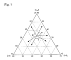
- Fig. 1 is a view to describe a concept of the present invention.
- a CZTS-based compound semiconductor whose band gap is reduced than that of the conventional CZTS is made.
- Such a CZTS compound semiconductor can be obtained by, for example, having the CZTS-based compound semiconductor within the area shown by ⁇ in Fig. 1 .
- a CZTS-based compound semiconductor whose band gap is reduced compared with the conventional CZTS is made.
- Such a CZTS-based compound semiconductor can be obtained by, for example, having the CZTS-based compound semiconductor within the area shown by ⁇ in Fig. 1 .
- a CZTS-based compound semiconductor whose band gap is reduced compared with the conventional CZTS is obtained.
- the reason why it is possible to reduce the band gap of the CZTS-based compound semiconductor with such a configuration is that the lattice constant of the CZTS-based compound semiconductor becomes large.
- a CZTS-based compound semiconductor whose band gap is increased compared with the conventional CZTS is made.
- Such a CZTS-based compound semiconductor can be obtained by, for example, having the CZTS-based compound semiconductor within the area shown by ⁇ in Fig. 1 .
- a CZTS-based compound semiconductor whose band gap is increased compared with the conventional CZTS is made.
- Such a CZTS-based compound semiconductor can be obtained by, for example, having the CZTS-based compound semiconductor within the area shown by ⁇ in Fig. 1 .
- Methods for synthesizing a CZTS prepared with these law materials are not particularly limited, and for example, a method of: forming a sputter film of metal precursor; thereafter sulfurizing the resulting material in H 2 S gas, a method of: melting sulfide powder by a solvent to print and form a film; thereafter firing and sulfurizing the resulting material in H 2 S gas, a method of: mixing a sulfide powder; then synthesize the mixture to print; thereafter firing and sulfurizing the resulting material in H 2 S gas, a method of: synthesizing CZTS particles by a chemical liquid-phase synthesis; after that printing and firing the resulting material to sulfurize it in H 2 S gas and the like can be exemplified.
- band gaps can be changed with the CZTS-related elements, by employing same manners (temperature, handling method and the like) in the producing process, it is possible to produce a plurality of CZTS-based compound semiconductors having different band gaps. Therefore, it is possible to produce a photoelectric conversion device that is stable in performance at low cost.
- the mixing ratios of Cu 2 S, ZnS and SnS 2 in Table 1 are shown being rounded off to two decimal places, and for convenience, ratio of Cu (rate of Cu to the total amount of Cu, Zn and Sn), ratio of Zn (rate of Zn to the total amount of Cu, Zn and Sn) and ratio of Sn (rate of Sn to the total amount of Cu, Zn and Sn) are shown being rounded off to three decimal places.
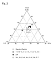
- Mixing ratios of raw materials of each synthetic powder are also shown in Fig. 2 . [Table 1] Sample No.
- each synthetic powder had peaks at same positions, and each had a CZTS single composition. Also, as shown in Figs. 5 and 6 , each synthetic powder showed a different optical characteristic from others. It is considered that this is because the synthetic powders have different band gaps, as shown in Table 1.
- the present invention it is possible to provide a CZTS-based compound semiconductor whose band gap is different from that of the conventional CZTS-based compound semiconductor. Also, by employing such a CZTS-based compound semiconductor, it becomes possible to configure a multi-junction solar cell in which a plurality of CZTS-based compound semiconductors having different band gaps are layered. Therefore, according to the present invention, it is also possible to provide a photoelectric conversion device in which the conversion efficiency is improved.
Landscapes
- Chemical & Material Sciences (AREA)
- Organic Chemistry (AREA)
- Inorganic Chemistry (AREA)
- Photovoltaic Devices (AREA)
- Life Sciences & Earth Sciences (AREA)
- Crystallography & Structural Chemistry (AREA)
- Sustainable Development (AREA)
- Engineering & Computer Science (AREA)
- Manufacturing & Machinery (AREA)
Abstract
Description
- The present invention relates to a CZTS-based compound semiconductor and a photoelectric conversion device prepared with the CZTS-based compound semiconductor.
- A solar cell has advantages that the amount of carbon dioxide emitted per power generation amount is small and it is not necessary to use fuel for power generation. Therefore, solar cells have been hoped as an energy source to inhibit global warming. Currently, among the solar cells in practical use, a mono-junction solar cell having a pair of p-n junction and using a single-crystal silicon or a polycrystal silicon has become a mainstream. Other than this, nowadays, studies on thin film solar cells and the like that do not depend on silicon have been actively developed.
- A CZTS-based thin film solar cell is a solar battery in which Cu, Zn, Sn and S (hereinafter sometimes referred to as "CZTS-based material". Also, hereinafter, a compound semiconductor prepared with the CZTS-based material is referred to as "CZTS-based compound semiconductor".) are used for its light absorbing layer, instead of silicon. Since these are easily available and inexpensive, Cu, Zn, Sn and S are expected as materials of a light absorbing layer of thin film solar cells.
- As a related art of the CZTS-based thin film solar cell, for example, Patent Document 1 discloses a sulfide compound semiconductor containing Cu, Zn, Sn and S but not containing a material including Na and O, and a photoelectric device in which the sulfide compound semiconductor is used for its light absorbing layer.
- Patent Document 1: Japanese Patent Application Laid-Open (JP-A) No.
2009-26891 - A conventional Cu2ZnSnS4 as disclosed in Patent Document 1 (hereinafter, sometimes referred to as "CZTS") has a band gap of around 1.45 eV. In order to improve conversion efficiency of the CZTS-based thin film solar cell, it is desired that the cell absorbs a wide range of wavelength of solar light to generate electricity. However, since the composition material of Cu2ZnSnS4 itself that has been discovered until now only has a single band gap, range of solar light to be absorbed is limited. In order to develop a CZTS-based thin film solar cell that can absorb a wide range of wavelength of solar light, it can be considered that it is effective to configure a so-called multi-junction solar cell in which a plurality of CZTS-based materials having different band gaps are laminated. However, a changing/adjusting method of band gap in the CZTS-based material has not been found out until now, and the changing/adjusting method of band gap in the CZTS-based material has not been established. For this reason, the multi-junction solar cell in which a plurality of CZTS-based materials having different band gaps could not be configured.
- Accordingly, an object of the present invention is to provide a CZTS-based compound semiconductor whose band gap is different from that of a conventional CZTS-based compound semiconductor and a photoelectric conversion device prepared with the CZTS-based compound semiconductor.
- The inventors of the present invention, as a result of an intensive study, have found out that it is possible to obtain a CZTS-based compound semiconductor whose band gap is different from that of a conventional CZTS by having a ratio of Cu, Zn and Sn configuring the CZTS-based compound semiconductor different from the ratio of Cu, Zn and Sn configuring the conventional Cu2ZnSnS4. More specifically, they have found out that it becomes possible to obtain a CZTS-based compound semiconductor whose band gap is reduced compared with the conventional CZTS by, comparing with the conventional CZTS, (1) increasing content ratio of Cu to raise the upper end of the valence band (VBM), (2) reducing content ratio of Sn to lower the lower end of the conducting band (CBM), (3) substituting Zn partially with an element having a larger ionic radius than an ionic radius of Zn, which element is to be a divalent ion (for example, Ca, Sr, Ba and the like). They also have found out that it becomes possible to obtain a CZTS-based compound semiconductor whose band gap is increased compared with the conventional CZTS by, comparing with the conventional CZTS, (4) reducing content ratio of Cu to lower the upper end of the valence band (VBM), (5) increasing content ratio of Sn to raise the lower end of the conducting band (CBM), (6) substituting Zn partially with an element having a smaller ionic radius than an ionic radius of Zn, which element is to be a divalent ion (for example, Mg, Be and the like) . The present invention has been made based on the above findings.
- In order to solve above problems, the present invention takes the following means. That is, a first aspect of the present invention is a CZTS-based compound semiconductor having a larger ratio of the number of moles of Cu to the total number of moles of Cu, Zn and Sn than a ratio of the number of moles of Cu to the total number of moles of Cu, Zn and Sn configuring Cu2ZnSnS4. By making the ratio of the number of moles of Cu larger, it is possible to raise the upper end of the valence band (VBM), therefore it is possible to obtain a CZTS-based compound semiconductor whose band gap is reduced compared with the conventional CZTS.
- Also, in the first aspect of the present invention, additionally, a ratio of the number of moles of Zn to the total number of moles of Cu, Zn and Sn can be made smaller than a ratio of the number of moles of Zn to the total number of moles of Cu, Zn and Sn configuring Cu2ZnSnS4. With such a configuration, it is possible to obtain a CZTS-based compound semiconductor whose band gap is reduced compared with the conventional CZTS.
- A second aspect of the present invention is a CZTS compound semiconductor having a smaller ratio of the number of moles of Zn to the total number of moles of Cu, Zn and Sn than a ratio of the number of moles of Zn to the total number of moles of Cu, Zn and Sn configuring Cu2ZnSnS4. By making the ratio of number of moles of Zn smaller to make a ratio of the number of moles of Cu and Sn larger for example, it is possible to obtain a CZTS-based compound semiconductor whose band gap is reduced compared with the conventional CZTS.
- A third aspect of the present invention is a CZTS compound semiconductor having a smaller ratio of the number of moles of Sn to the total number of moles of Cu, Zn and Sn than a ratio of the number of moles of Sn to the total number of moles of Cu, Zn and Sn configuring Cu2ZnSnS4. By making the ratio of the number of moles of Sn small, it is possible to lower the lower end of the conducting band (CBM), therefore it is possible to obtain a CZTS-based compound semiconductor whose band gap is reduced compared with the conventional CZTS.
- A fourth aspect of the present invention is a CZTS-based compound semiconductor comprising a part of Zn configuring Cu2ZnSnS4, the part being substituted by an element having a larger ionic radius than an ionic radius of Zn, the element being to be a divalent ion (for instance, Ca, Sr, Ba and the like). By substituting Zn partially with Ca, Sr, Ba or the like, it is possible to obtain a CZTS-based compound semiconductor whose band gap is reduced compared with the conventional CZTS.
- A fifth aspect of the present invention is a CZTS-based compound semiconductor having a smaller ratio of the number of moles of Cu to the total number of moles of Cu, Zn and Sn than a ratio of the number of moles of Cu to the total number of moles of Cu, Zn and Sn configuring Cu2ZnSnS4. By making the ratio of the number of moles of Cu smaller, it is possible to lower the upper end of the valence band (VBM), therefore it is possible to obtain a CZTS-based compound semiconductor whose band gap is increased compared with the conventional CZTS.
- Also, in the fifth aspect of the present invention, additionally, it is preferable to make a ratio of the number of moles of Sn to the total numbers of moles of Cu, Zn and Sn larger than a ratio of the number of moles of Sn to the total number of the moles of Cu, Zn and Sn configuring Cu2ZnSnS4. With such a configuration, it becomes easy to obtain a CZTS-based compound semiconductor whose band gap is increased compared with the conventional CZTS.
- A sixth aspect of the present invention is a CZTS-based compound semiconductor having a larger ratio of the number of moles of Sn to the total number of moles of Cu, Zn and Sn than a ratio of the number of moles of Sn to the total number of moles of Cu, Zn and Sn configuring Cu2ZnSnS4. By making the ratio of the number of moles of Su larger, it is possible to raise the lower end of the conducting band (CBM), therefore it is possible to obtain a CZTS-based compound semiconductor whose band gap is increased compared with the conventional CZTS.
- A seventh aspect of the present invention is a CZTS-based compound semiconductor comprising a part of Zn configuring Cu2ZnSnS4, the part being substituted by an element having a smaller ionic radius than an ionic radius of Zn, the element being to be a divalent ion. (for example, Mg, Be and the like). By substituting Zn partially with Mg, Be or the like, it is possible to obtain a CZTS compound semiconductor whose band gap is increased compared with the conventional CZTS.
- An eighth aspect of the present invention is a photoelectric conversion device comprising a plurality of CZTS-based compound semiconductors having different band gaps, wherein the CZTS-based compound semiconductor according to the first to the seventh aspects of the present invention is included in the plurality of CZTS-based compound semiconductors. With such a configuration, it is possible to configure a multi-junction solar cell in which a plurality of CZTS materials having different band gaps are laminated, therefore it is possible to provide a photoelectric conversion device that can absorb a wide range of wavelengths of solar light.
- According to the present invention, it is possible to provide a CZTS-based compound semiconductor whose band gap is different from that of the conventional CZTS-based compound semiconductor and a manufacturing method of the CZTS-based compound semiconductor, and a photoelectric conversion device prepared with the CZTS-based compound semiconductor and a manufacturing method of the photoelectric conversion device.
-
-
Fig. 1 is a view to describe a concept of the present invention; -
Fig. 2 is a view to describe a composition of a CZTS-based compound semiconductor; -
Fig. 3 is a graph showing results of X-ray diffraction of synthetic powders; -
Fig. 4 is a graph showing results of X-ray diffraction of synthetic powders; -
Fig. 5 is a graph showing results of optical characteristic measurement; -
Fig. 6 is a graph showing results of optical characteristic measurement. - Hereinafter, the present invention will be described with reference to the drawings. It should be noted that the embodiments shown below is examples of the present invention, and the present invention is not limited to the embodiments.
-
Fig. 1 is a view to describe a concept of the present invention. As described above, in the present invention, for example, by increasing content ratio of Cu to raise the upper end of the valence band (VBM) comparing with the conventional CZTS, a CZTS-based compound semiconductor whose band gap is reduced than that of the conventional CZTS is made. Such a CZTS compound semiconductor can be obtained by, for example, having the CZTS-based compound semiconductor within the area shown by α inFig. 1 . - Also, in the present invention, for instance, by reducing content ratio of Sn to lower the lower end of the conducting band (CBM) than the conventional CZTS, a CZTS-based compound semiconductor whose band gap is reduced compared with the conventional CZTS is made. Such a CZTS-based compound semiconductor can be obtained by, for example, having the CZTS-based compound semiconductor within the area shown by β in
Fig. 1 . - Also, in the present invention, for example, by substituting Zn partially with an element having a larger ionic radius than an ionic radius of Zn, which element is to be a divalent ion (for example, Ca, Sr, Ba and the like), a CZTS-based compound semiconductor whose band gap is reduced compared with the conventional CZTS is obtained. The reason why it is possible to reduce the band gap of the CZTS-based compound semiconductor with such a configuration is that the lattice constant of the CZTS-based compound semiconductor becomes large.
- In addition, in the present invention, for example, by reducing the content ratio of Cu to lower the upper end of the valence band (VBM) comparing with the conventional CZTS, a CZTS-based compound semiconductor whose band gap is increased compared with the conventional CZTS is made. Such a CZTS-based compound semiconductor can be obtained by, for example, having the CZTS-based compound semiconductor within the area shown by γ in
Fig. 1 . - Also, in the present invention, for example, by increasing the content ratio of Sn comparing with the conventional CZTS to raise the lower end of the conducting band (CBM), a CZTS-based compound semiconductor whose band gap is increased compared with the conventional CZTS is made. Such a CZTS-based compound semiconductor can be obtained by, for example, having the CZTS-based compound semiconductor within the area shown by γ in
Fig. 1 . - Also, in the present invention, for example, by substituting Zn partially with an element having a smaller ionic radius than an ionic radius of Zn, which element is to be a divalent ion (for example, Mg, Be and the like), a CZTS-based compound semiconductor whose band gap is increased compared with the conventional CZTS is obtained. The reason why it is possible to increase the band gap of the CZTS-based compound semiconductor with such a configuration is that the lattice constant of the CZTS-based compound semiconductor becomes small.
- It is possible to reach the areas shown by α, β, and γ in
Fig. 1 by adequately adjusting mixing ratio of Cu2S, ZnS and SnS2. It is possible to produce the CZTS-based compound semiconductor of the present invention whose band gap is different from the conventional CZTS, for example, by using Cu2S, ZnS and SnS2 whose mixing ratio is adjusted. Methods for synthesizing a CZTS prepared with these law materials are not particularly limited, and for example, a method of: forming a sputter film of metal precursor; thereafter sulfurizing the resulting material in H2S gas, a method of: melting sulfide powder by a solvent to print and form a film; thereafter firing and sulfurizing the resulting material in H2S gas, a method of: mixing a sulfide powder; then synthesize the mixture to print; thereafter firing and sulfurizing the resulting material in H2S gas, a method of: synthesizing CZTS particles by a chemical liquid-phase synthesis; after that printing and firing the resulting material to sulfurize it in H2S gas and the like can be exemplified. - According to the present invention, since band gaps can be changed with the CZTS-related elements, by employing same manners (temperature, handling method and the like) in the producing process, it is possible to produce a plurality of CZTS-based compound semiconductors having different band gaps. Therefore, it is possible to produce a photoelectric conversion device that is stable in performance at low cost.
- Hereinafter, the present invention will be further specifically described with reference to Examples and Comparative Examples.
- Each powder of Cu2S (manufactured by Kojundo Chemical Laboratory Co., LTD), ZnS (manufactured by Kojundo Chemical Laboratory Co., LTD) and SnS2 (manufactured by Kojundo Chemical Laboratory Co., LTD) was measured in a predetermined amount and put in a ball mill. Subsequently, 50 vol% of ethanol was put in the ball mill and contents of the ball mill were mixed for 24 hours. After that, the resulting material was dried at 120°C for 10 hours to obtain a powder. The obtained powder was put into a glass tube, and vacuum drawing was carried out followed by substitution by nitrogen gas. By heating and sealing the glass tube, a glass capsule was produced. Thereafter, the produced glass capsule was put in an electrical furnace (manufactured by Yamato Scientific Co. , LTD) and heating treatment was carried out at 700°C for 5 hours whereby a synthetic powder was produced. Mixing ratios of Cu2S, ZnS and SnS2 in cases where the total amount of Cu2S, ZnS and SnS2 is defined as 1 are shown in Table 1. The mixing ratios of Cu2S, ZnS and SnS2 in Table 1 are shown being rounded off to two decimal places, and for convenience, ratio of Cu (rate of Cu to the total amount of Cu, Zn and Sn), ratio of Zn (rate of Zn to the total amount of Cu, Zn and Sn) and ratio of Sn (rate of Sn to the total amount of Cu, Zn and Sn) are shown being rounded off to three decimal places. Mixing ratios of raw materials of each synthetic powder are also shown in
Fig. 2 .[Table 1] Sample No. Cu2S ZnS SnS2 Ratio of Cu Ratio of Zn Ratio of Sn Eg [eV] Standard Sample 0.33 0.33 0.33 0.500 0.250 0.250 1.46 1-1 0.34 0.31 0.36 0.504 0.230 0.267 1.14 1-2 0.36 0.29 0.36 0.526 0.212 0.263 1.12 1-3 0.34 0.28 0.38 0.507 0.209 0.284 1.11 1-4 0.38 0.24 0.38 0.551 0.174 0.275 1.09 2-1 (= 1-1) 0.34 0.31 0.36 0.504 0.230 0.267 1.14 2-2 0.36 0.29 0.36 0.526 0.212 0.263 1.12 2-3 0.36 0.28 0.38 0.522 0.203 0.275 1.11 2-4 0.29 0.42 0.29 0.450 0.326 0.225 1.34 3-1 0.31 0.34 0.34 0.477 0.262 0.262 1.51 3-2 0.29 0.36 0.36 0.446 0.277 0.277 1.55 3-3 0.31 0.33 0.36 0.473 0.252 0.275 1.50 3-4 0.29 0.31 0.39 0.453 0.242 0.305 1.53 3-5 0.26 0.37 0.37 0.413 0.294 0.294 1.60 3-6 0.26 0.35 0.39 0.413 0.278 0.310 1.66 3-7 0.26 0.33 0.41 0.413 0.262 0.325 1.71 - By carrying out X-ray diffraction measurement by means of a powder X-ray diffractometer (RINT2000, manufactured by Rigaku Corporation), it was confirmed that each produced synthetic powder has a single composition. Results of the X-ray diffraction of each synthetic powder of Standard sample, Sample No. 1-4, and Sample No. 2-3 are shown in
Fig. 3 . From upper side of plane of paper ofFig. 3 , the Results of Standard sample, Sample No. 1-4, and Sample No. 2-3 are shown in the order mentioned. Also, results of the X-ray diffraction of each synthetic powder of Standard sample and Sample No. 3-3 are shown inFig. 4 . From upper side of plane of paper ofFig. 4 , results of Standard Sample and Sample No. 3-3 are shown in the order mentioned. Intensity [arb.unit] is taken along the vertical axis, and 2θ [deg] is taken along the horizontal axis of each graph of theFigs. 3 and4 . - By carrying out an optical characteristic measurement by means of an ultraviolet visible near infrared spectrophotometer (LAMBDA 950, manufactured by PerkinElmer Inc.), a band gap of each of the produced synthetic powder was identified. Identified band gaps (Eg[eV]) are shown in Table 1. The band gaps Eg [eV] in Table 1 are shown being rounded off to two decimal places. Also, results of the optical characteristic measurement of each synthetic powder of Standard sample, Sample No. 1-4 and Sample No. 2-3 are shown in
Fig. 5 . and results of the optical characteristic measurement of each synthetic powder of Standard sample and Sample No. 3-3 are shown inFig. 6 . Intensity KM [a.u.] of light converted by Kubelka-Munk formula is taken along the vertical axis, and its wavelength [nm] is taken along the horizontal axis of the graphs ofFigs. 5 and6 . - As shown in
Figs. 3 and4 , all the produced synthetic powder had peaks at same positions, and each had a CZTS single composition. Also, as shown inFigs. 5 and6 , each synthetic powder showed a different optical characteristic from others. It is considered that this is because the synthetic powders have different band gaps, as shown in Table 1. - By comparing Table 1 and
Fig. 2 withFig. 1 , it was found out that a CZTS-based compound semiconductor in which the band gap is greatly reduced (band gap: between 1. 09 eV and 1. 14 eV inclusive) can be obtained by having the CZTS-based compound semiconductor within the area shown by α inFig. 1 . Also, it was found out that a CZTS-based compound semiconductor in which the band gap is reduced (band gap: between 1.3 eV and 1. 4 eV inclusive) can be obtained by having the CZTS-based compound semiconductor within the area shown by β inFig. 1 . It was also found out that a CZTS-based compound semiconductor whose band gap is increased (band gap: between 1.50 eV and 1.71 eV inclusive) can be obtained by having the CZTS-based compound semiconductor within the area shown by γ inFig. 1 . - As described above, according to the present invention, it is possible to provide a CZTS-based compound semiconductor whose band gap is different from that of the conventional CZTS-based compound semiconductor. Also, by employing such a CZTS-based compound semiconductor, it becomes possible to configure a multi-junction solar cell in which a plurality of CZTS-based compound semiconductors having different band gaps are layered. Therefore, according to the present invention, it is also possible to provide a photoelectric conversion device in which the conversion efficiency is improved.
Claims (10)
- A CZTS-based compound semiconductor having a larger ratio of the number of moles of Cu to the total number of moles of Cu, Zn and Sn than a ratio of the number of moles of Cu to the total number of moles of Cu, Zn and Sn configuring Cu2ZnSnS4.
- The CZTS-based compound semiconductor according to claim 1, wherein a ratio of the number of moles of Zn to the total number of moles of Cu, Zn and Sn is smaller than a ratio of the number of moles of Zn to the total number of moles of Cu, Zn and Sn configuring Cu2ZnSnS4.
- A CZTS-based compound semiconductor having a smaller ratio of the number of moles of Zn to the total number of moles of Cu, Zn and Sn than a ratio of the number of moles of Zn to the total number of moles of Cu, Zn and Sn configuring Cu2ZnSnS4.
- A CZTS-based compound semiconductor having a smaller ratio of the number of moles of Sn to the total number of moles of Cu, Zn and Sn than a ratio of the number of moles of Sn to the total number of moles of Cu, Zn and Sn configuring Cu2ZnSnS4.
- A CZTS-based compound semiconductor comprising a part of Zn configuring Cu2ZnSnS4, the part being substituted by an element having a larger ionic radius than an ionic radius of Zn, the element being to be a divalent ion.
- A CZTS-based compound semiconductor having a smaller ratio of the number of moles of Cu to the total number of moles of Cu, Zn and Sn than a ratio of the number of moles of Cu to the total number of moles of Cu, Zn and Sn configuring Cu2ZnSnS4.
- The CZTS-based compound semiconductor according to claim 6, wherein a ratio of the number of moles of Sn to the total number of moles of Cu, Zn and Sn is larger than a ratio of the number of moles of Sn to the total number of moles of Cu, Zn and Sn configuring Cu2ZnSnS4.
- A CZTS-based compound semiconductor having a larger ratio of the number of moles of Sn to the total number of moles of Cu, Zn and Sn than a ratio of the number of moles of Sn to the total number of moles of Cu, Zn and Sn configuring Cu2ZnSnS4.
- A CZTS-based compound semiconductor comprising a part of Zn configuring Cu2ZnSnS4, the part being substituted by an element having a smaller ionic radius than an ionic radius of Zn, the element being to be a divalent ion.
- A photoelectric conversion device comprising a plurality of CZTS-based compound semiconductors having different band gaps, wherein the CZTS-based compound semiconductor according to any one of claims 1 to 9 is included in the plurality of CZTS-based compound semiconductors.
Applications Claiming Priority (2)
| Application Number | Priority Date | Filing Date | Title |
|---|---|---|---|
| JP2011288625A JP2013136481A (en) | 2011-12-28 | 2011-12-28 | Czts-based compound semiconductor and photoelectric transducer |
| PCT/JP2012/081060 WO2013099517A1 (en) | 2011-12-28 | 2012-11-30 | Czts-based compound semiconductor and photoelectric transducer |
Publications (2)
| Publication Number | Publication Date |
|---|---|
| EP2799399A1 true EP2799399A1 (en) | 2014-11-05 |
| EP2799399A4 EP2799399A4 (en) | 2015-07-08 |
Family
ID=48697015
Family Applications (1)
| Application Number | Title | Priority Date | Filing Date |
|---|---|---|---|
| EP12862311.3A Withdrawn EP2799399A4 (en) | 2011-12-28 | 2012-11-30 | CZTS COMPOUND SEMICONDUCTOR AND CORRESPONDING PHOTOELECTRIC TRANSDUCER |
Country Status (5)
| Country | Link |
|---|---|
| US (1) | US20140332080A1 (en) |
| EP (1) | EP2799399A4 (en) |
| JP (1) | JP2013136481A (en) |
| CN (1) | CN104039707A (en) |
| WO (1) | WO2013099517A1 (en) |
Family Cites Families (8)
| Publication number | Priority date | Publication date | Assignee | Title |
|---|---|---|---|---|
| JP4783908B2 (en) | 2007-07-18 | 2011-09-28 | 株式会社豊田中央研究所 | Photoelectric element |
| US8580157B2 (en) * | 2009-02-20 | 2013-11-12 | Kabushiki Kaisha Toyota Chuo Kenkyusho | Sulfide and photoelectric element |
| US9028723B2 (en) * | 2009-02-27 | 2015-05-12 | National University Corporation Nagoya University | Semiconductor nanoparticles and method for producing same |
| JP2012527523A (en) * | 2009-05-21 | 2012-11-08 | イー・アイ・デュポン・ドウ・ヌムール・アンド・カンパニー | Copper tin sulfide and copper zinc tin sulfide ink composition |
| US20120219797A1 (en) * | 2009-08-06 | 2012-08-30 | Mitsui Mining & Smelting Co., Ltd. | Semiconductor Powder and Method for Producing the Same |
| JP2013512174A (en) * | 2009-11-25 | 2013-04-11 | イー・アイ・デュポン・ドウ・ヌムール・アンド・カンパニー | Synthesis of quaternary chalcogenides in fluxes containing cesium, rubidium, barium, and lanthanum |
| JP5641284B2 (en) * | 2010-02-03 | 2014-12-17 | 独立行政法人国立高等専門学校機構 | Compound semiconductor, photoelectric device and manufacturing method thereof |
| JP5454213B2 (en) * | 2010-02-22 | 2014-03-26 | Tdk株式会社 | Method for producing compound semiconductor light absorption layer and method for producing compound semiconductor thin film solar cell |
-
2011
- 2011-12-28 JP JP2011288625A patent/JP2013136481A/en active Pending
-
2012
- 2012-11-30 CN CN201280063360.5A patent/CN104039707A/en active Pending
- 2012-11-30 WO PCT/JP2012/081060 patent/WO2013099517A1/en not_active Ceased
- 2012-11-30 US US14/364,870 patent/US20140332080A1/en not_active Abandoned
- 2012-11-30 EP EP12862311.3A patent/EP2799399A4/en not_active Withdrawn
Also Published As
| Publication number | Publication date |
|---|---|
| JP2013136481A (en) | 2013-07-11 |
| CN104039707A (en) | 2014-09-10 |
| WO2013099517A1 (en) | 2013-07-04 |
| US20140332080A1 (en) | 2014-11-13 |
| EP2799399A4 (en) | 2015-07-08 |
Similar Documents
| Publication | Publication Date | Title |
|---|---|---|
| Li et al. | Achieving 11.95% efficient Cu 2 ZnSnSe 4 solar cells fabricated by sputtering a Cu–Zn–Sn–Se quaternary compound target with a selenization process | |
| Washio et al. | 6% Efficiency Cu 2 ZnSnS 4-based thin film solar cells using oxide precursors by open atmosphere type CVD | |
| Yeom et al. | Controllable synthesis of single crystalline Sn-based oxides and their application in perovskite solar cells | |
| Nguyen et al. | Cu 2 ZnSnS 4 thin film solar cells with 5.8% conversion efficiency obtained by a facile spray pyrolysis technique | |
| KR101179010B1 (en) | Chalcogenide semiconductor thin film and fabrication method thereof | |
| TWI455333B (en) | Solar battery | |
| EP3679607B1 (en) | Organic-inorganic perovskite materials and methods of making the same | |
| US20130240797A1 (en) | Compound semiconductor | |
| JP6330051B2 (en) | Method for doping Cu (In, Ga) (S, Se) 2 nanoparticles with sodium or antimony | |
| CN105705596A (en) | I inorganic salt-nanoparticle ink for thin film photovoltaic devices and related methods | |
| Huang et al. | Perovskite-quantum dot hybrid solar cells: a multi-win strategy for high performance and stability | |
| CN103633165B (en) | Yellow copper structure Intermediate Gray solar battery obsorbing layer material and preparation method thereof | |
| Lin et al. | Antimony loss and composition-dependent phase evolution of CuSbS2 absorber using oxides nanoparticles ink | |
| WO2020081412A1 (en) | Two-dimensional perovskites for stable and efficient photovoltaic cells | |
| KR101388432B1 (en) | Se or s based thin film solar cell and method for fabricating the same | |
| EP2799399A1 (en) | Czts-based compound semiconductor and photoelectric transducer | |
| Shiu et al. | Solution-processed all-oxide nanostructures for heterojunction solar cells | |
| WO2025094603A1 (en) | Method for manufacturing solar cell, and solar cell | |
| CN103606573B (en) | A kind of Intermediate Gray absorbing material of yellow copper structure and preparation method thereof | |
| WO2013099180A1 (en) | Photovoltaic conversion device and method of manufacturing photovoltaic conversion material | |
| Mu et al. | Electrospun Cu 2 ZnSnS 4 microfibers with strong (112) preferred orientation: fabrication and characterization | |
| Zhou et al. | Enhancement of Cu 2 ZnSn (S, Se) 4 device performance using an IPA/MOE hybrid solvent system in ambient air | |
| KR20130097903A (en) | Precursor for preparing the sns thin-film and manufacturing method thereof | |
| Salve et al. | Development of CdTe thin film solar cells using a hybrid wet chemical hydrothermal and doctor blade technique | |
| JP6775841B2 (en) | New compound semiconductors and their utilization |
Legal Events
| Date | Code | Title | Description |
|---|---|---|---|
| PUAI | Public reference made under article 153(3) epc to a published international application that has entered the european phase |
Free format text: ORIGINAL CODE: 0009012 |
|
| 17P | Request for examination filed |
Effective date: 20140610 |
|
| AK | Designated contracting states |
Kind code of ref document: A1 Designated state(s): AL AT BE BG CH CY CZ DE DK EE ES FI FR GB GR HR HU IE IS IT LI LT LU LV MC MK MT NL NO PL PT RO RS SE SI SK SM TR |
|
| RIN1 | Information on inventor provided before grant (corrected) |
Inventor name: SAKAI, TAKENOBU Inventor name: TAKAHASHI, SEIJI Inventor name: UEDA, TARO Inventor name: AWANO, HIROKI Inventor name: MAEKAWA, RYOSUKE |
|
| DAX | Request for extension of the european patent (deleted) | ||
| RA4 | Supplementary search report drawn up and despatched (corrected) |
Effective date: 20150610 |
|
| RIC1 | Information provided on ipc code assigned before grant |
Ipc: H01L 31/032 20060101ALI20150604BHEP Ipc: H01L 31/065 20120101ALI20150604BHEP Ipc: C01G 19/00 20060101AFI20150604BHEP Ipc: H01L 31/0725 20120101ALI20150604BHEP Ipc: H01L 21/02 20060101ALI20150604BHEP |
|
| STAA | Information on the status of an ep patent application or granted ep patent |
Free format text: STATUS: THE APPLICATION IS DEEMED TO BE WITHDRAWN |
|
| 18D | Application deemed to be withdrawn |
Effective date: 20160108 |