EP2798389B1 - Integrated circuit coupling system with waveguide circuitry and method of manufacture thereof - Google Patents
Integrated circuit coupling system with waveguide circuitry and method of manufacture thereof Download PDFInfo
- Publication number
- EP2798389B1 EP2798389B1 EP12863185.0A EP12863185A EP2798389B1 EP 2798389 B1 EP2798389 B1 EP 2798389B1 EP 12863185 A EP12863185 A EP 12863185A EP 2798389 B1 EP2798389 B1 EP 2798389B1
- Authority
- EP
- European Patent Office
- Prior art keywords
- optical
- clad
- photoresist
- mirror
- sidewalls
- Prior art date
- Legal status (The legal status is an assumption and is not a legal conclusion. Google has not performed a legal analysis and makes no representation as to the accuracy of the status listed.)
- Active
Links
Images



Classifications
-
- G—PHYSICS
- G02—OPTICS
- G02B—OPTICAL ELEMENTS, SYSTEMS OR APPARATUS
- G02B6/00—Light guides; Structural details of arrangements comprising light guides and other optical elements, e.g. couplings
- G02B6/24—Coupling light guides
- G02B6/26—Optical coupling means
- G02B6/30—Optical coupling means for use between fibre and thin-film device
-
- G—PHYSICS
- G02—OPTICS
- G02B—OPTICAL ELEMENTS, SYSTEMS OR APPARATUS
- G02B6/00—Light guides; Structural details of arrangements comprising light guides and other optical elements, e.g. couplings
- G02B6/10—Light guides; Structural details of arrangements comprising light guides and other optical elements, e.g. couplings of the optical waveguide type
- G02B6/12—Light guides; Structural details of arrangements comprising light guides and other optical elements, e.g. couplings of the optical waveguide type of the integrated circuit kind
- G02B6/13—Integrated optical circuits characterised by the manufacturing method
- G02B6/136—Integrated optical circuits characterised by the manufacturing method by etching
-
- G—PHYSICS
- G02—OPTICS
- G02B—OPTICAL ELEMENTS, SYSTEMS OR APPARATUS
- G02B6/00—Light guides; Structural details of arrangements comprising light guides and other optical elements, e.g. couplings
- G02B6/24—Coupling light guides
- G02B6/26—Optical coupling means
- G02B6/262—Optical details of coupling light into, or out of, or between fibre ends, e.g. special fibre end shapes or associated optical elements
-
- G—PHYSICS
- G02—OPTICS
- G02B—OPTICAL ELEMENTS, SYSTEMS OR APPARATUS
- G02B6/00—Light guides; Structural details of arrangements comprising light guides and other optical elements, e.g. couplings
- G02B6/24—Coupling light guides
- G02B6/26—Optical coupling means
- G02B6/34—Optical coupling means utilising prism or grating
-
- G—PHYSICS
- G02—OPTICS
- G02B—OPTICAL ELEMENTS, SYSTEMS OR APPARATUS
- G02B6/00—Light guides; Structural details of arrangements comprising light guides and other optical elements, e.g. couplings
- G02B6/24—Coupling light guides
- G02B6/42—Coupling light guides with opto-electronic elements
- G02B6/4201—Packages, e.g. shape, construction, internal or external details
- G02B6/4204—Packages, e.g. shape, construction, internal or external details the coupling comprising intermediate optical elements, e.g. lenses, holograms
- G02B6/4214—Packages, e.g. shape, construction, internal or external details the coupling comprising intermediate optical elements, e.g. lenses, holograms the intermediate optical element having redirecting reflective means, e.g. mirrors, prisms for deflecting the radiation from horizontal to down- or upward direction toward a device
Definitions
- the present invention relates generally to an integrated circuit coupling system, and more particularly to a system for routing optical signals.
- Monolithically integrated optical waveguide technology provides key components of recent and expected future improvements in telecommunications and other networks.
- Optical fiber networks are used to convey data in almost all applications where data rates exceed 1 Gb/sec and transmission distances exceed a few meters.
- Fiber optic networks pervade and enable the networks forming the internet.
- Coupling light in and out of PLCs is accomplished by routing the appropriate waveguides to the edge of the PLC substrate and mating optical fibers, photo detectors, or lasers to the waveguides at the substrate edges.
- the waveguides are defined within a single layer of the PLC and are allowed to cross, but practical waveguide crossings do exhibit small amounts of loss and crosstalk and that does add up for multiple crossings, so it is generally desirable to keep the number of crossings for any optical path to be less than the order of 10. Also, optical cores cannot be bent too sharply, minimum radius of curvature allowed is generally a few millimeters.
- Patent document WO 92/18888 describes a method for forming an optical waveguide structure comprising the steps of forming a cladding layer upon a substrate, forming the optical waveguide structure by using an erodible mask and subsequent etch, and placing optical waveguide material within a volume of the optical waveguide structure.
- Patent document US 2009/0214170 A1 describes a method for making a planar lightwave circuit waveguide comprising the steps of etching a substrate to form a slanted wall, forming a non-reflective waveguide portion on the substrate, and depositing a reflective layer on the slanted wall.
- Patent document US 4,698,128 describes a method for providing a sloped contact etch comprising the steps of etching a substrate in an area defined by a resist layer, removing a polymer produced during the etching, etching the resist layer, thereby increasing the area defined by the resist layer, and etching the substrate in the area defined by the resist layer.
- the present invention provides a method of manufacture of an integrated circuit coupling system including: forming a waveguide assembly, having a top clad over an open end of an optical core; forming a first photoresist having a base photoresist pattern shape with sloped photoresist sidewalls tapered down to expose a portion of the top clad; forming a recess having clad sidewalls from the portion of the top clad exposed by the base photoresist pattern shape, the clad sidewalls having a shape replicating a shape of the base photo resist pattern shape; and forming an optical vertical insertion area, from the clad sidewalls forming the recess, having a pocket trench, a horizontal step, and a mirror with a reflective material selectively applied to a section of the clad sidewalls and exposing the open end opposite to the mirror, the horizontal step between the mirror and the pocket trench.
- the present invention provides an integrated circuit coupling system, including: a top clad having clad sidewalls over the substrate; an optical core having an open end between the substrate and the top clad; and an optical vertical insertion area having a mirror, a horizontal step, and a pocket trench formed, through the top clad, below and between the open end and the mirror opposite the open end exposed in the optical vertical insertion area, the horizontal step between the mirror and the pocket trench.
- the term “horizontal” as used herein is defined as a plane parallel to the plane or surface of the substrate below an optical core, regardless of its orientation.
- the term “vertical” refers to a direction perpendicular to the horizontal as just defined. Terms, such as “above”, “below”, “bottom”, “top”, “side” (as in “sidewall”), “higher”, “lower”, “upper”, “over”, and “under”, are defined with respect to the horizontal plane, as shown in the figures.
- the term “on” means that there is direct contact between two elements and there is no other intervening element between the direct contact of the two elements.
- processing includes deposition of material or photoresist, patterning, exposure, development, etching, cleaning, and/or removal of the material or photoresist as required in forming a described structure.
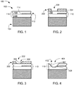
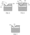
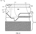
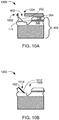
- FIG. 1 therein is shown a partial cross-sectional view of an integrated circuit coupling system 100 in a manufacturing step of a first embodiment of the present invention.
- an exemplary planar lightwave circuit 102 also referred to as the PLC 102, having a substrate 104, a bottom clad 106, a top clad 108, and an optical core 112.
- the bottom clad 106 and the top clad 108 can include silica or glass.
- the substrate 104 such as a silicon wafer or quartz wafer, is covered with a silica layer that functions as the bottom clad 106 to isolate the light in the optical core 112, also referred to as the silica waveguide channel, from the substrate 104.
- a deposited layer of doped silica is used to provide the top-clad 108 with side clad for the optical core 112.
- An open end 114 of the optical core 112 between the top clad 108 and the bottom clad 106 is sealed by the top clad 108.
- the optical core 112 with the open end 114, the top clad 108, and the bottom clad 106 can be referred to as a waveguide assembly 110.
- the optical core 112, the bottom clad 106, and the top clad 108 can have various thicknesses.
- the actual thicknesses are very tightly controlled, but across most typical applications, they fall in the following exemplary ranges.
- a thickness of the optical core 112 is typically in the range of four to six microns.
- a layer thickness of the bottom clad 106 is typically in the range ten to twenty microns, for example.
- a thickness of the top clad 108 is such that its upper surface is ten to twenty microns above an upper surface of the waveguide core.
- the thicknesses previously described above are examples only, it is understood that they are not intended to show any kind of order, connection, or order of manufacture.
- FIG. 2 therein is shown the partial cross-sectional view of the structure of FIG. 1 after deposition and photolithographic processing of a first photoresist 202.
- the photolithographic processing can include binary patterning of the first photoresist 202.
- the first photoresist 202 also referred to as base photoresist, can be deposited on an upper clad surface 204 of the top clad 108 of the waveguide assembly 110.
- the first photoresist 202 can be patterned to preserve, by covering, most of the upper clad surface 204 of the PLC 102 surface except for a small open region 208 of the first photoresist 202 exposing at least a portion of the upper clad surface 204 to be etched or removed in later processing steps.
- the first photoresist 202 can be, for example, formed of a polymer photoresist.
- FIG. 3 therein is shown the partial cross-sectional view of the structure of FIG. 2 after further processing the first photoresist 202.
- a photoresist layer is not commonly baked aggressively, or not baked at all, in this process sequence the first photoresist 202 can be baked for an extended time.
- the first photoresist 202 can be baked for 2.5 hours at 110 degrees Celsius.
- the baking can cause the first photoresist 202 to reflow, producing a base photoresist pattern shape 302 of the first photoresist 202 having sloped photoresist sidewalls 304 that enclose and taper down to a cross-sectional area of the small open region 208 of FIG. 2 .
- a cross-sectional area of the base photoresist pattern shape 302 above the upper clad surface 204 is larger than the cross-sectional area of the small open region 208 as a result of the narrowing and taper down of the sloped photoresist sidewalls 304.
- the sloped photoresist sidewalls 304 expose a portion of the upper clad surface 204 of FIG. 2 laterally offset away from the optical core 112 and opposite the open end 114.
- the sloped photoresist sidewalls 304 can be formed having an inclination angle 308, relative to a horizontal plane, pre-determined by user specifications, as a result of the controlled reflow of the first photoresist 202, characteristic of the first photoresist 202 reflowed by bake process.
- FIG. 4 therein is shown the partial cross-sectional view of the structure of FIG. 3 after etching.
- a specific etching process can be used wherein the first photoresist 202 of FIG. 2 and the top clad 108 of FIG. 1 etch at about the same rate resulting in transference or replication of the base photoresist pattern shape 302 of FIG. 2 into the top clad 108 and a portion of the bottom clad 106 of FIG. 1 .
- the etching can reproduce the sloped photoresist sidewalls 304 of FIG. 3 , at a desired slope angle ranging from 45 degrees and up relative to the horizontal plane containing the upper clad surface 204 of FIG. 2 , as clad sidewalls 402 of a recess 404 in the top clad 108 and a portion of the bottom clad 106.
- the clad sidewalls 402 formed into the waveguide assembly 110 can have a shape and a slope angle 412 equal to the base photoresist pattern shape 302 and the inclination angle 308 of FIG. 3 , respectively.
- the etching process can be to a depth below the upper clad surface 204 such that a bottom base 408 of the recess 404, having the clad sidewalls 402 intersecting the bottom base 408 formed through in the top clad 108, can extend two to five microns into the bottom clad 106. At this point, the optical core 103 can remain buried in the top clad 108.
- the clad sidewalls 402 and the slope angle 412 are characteristic of the specific etching process to form the clad sidewalls 402 with the slope angle 412 replicating the shape and the inclination angle 308 of the first photoresist 202, reflowed.
- the etching process can be different from standard PLC processing which can use reactive-ion etching processes that are typically associated with hardmask-directed etching.
- a normal etching process can scorch any photoresist, causing it to erode erratically and uncontrollably and substantially reducing the quality of the etching process.
- the parameters for Standard Etch of a vertical etch using hard mask are settings developed for a particular Reactive Ion Etching (RIE) machine model for a silica glass doped with 1-5% Boron and 1-5% Phosphorous, also referred to as Boron-Phosphorous Silica Glass or BPSG for etch depths between a few microns and a few tens of microns.
- RIE Reactive Ion Etching
- Example parameters for a Sloped Etch exemplary of those used for the present invention, are those that can give a good replication etch for the otherwise same conditions, such as in etching of the first photoresist 202 and the top clad 108 at the same rates in order to get the same shapes.
- FIG. 5 therein is shown the partial cross-sectional view of the structure of FIG. 4 after deposition of a hardmask 502.
- the hardmask 502 which can be produced from various materials, is layered on an interior of the recess 404 and on the upper clad surface 204 of the top clad 108.
- a thin layer of suitable hardmask material such as about 5000 angstroms of amorphous silicon, TiO2 or Aluminum, can be deposited to form the hardmask 502.
- the hardmask 502 is so called because it etches much more slowly than claddings or photoresist during applicable etch processes, protecting anything it covers from the etch process.
- FIG. 6 therein is shown the partial cross-sectional view of the structure of FIG. 5 after deposition, patterning, and photolithographic processing of a second photoresist 602.
- the second photoresist 602 can be applied on the hardmask 502.
- a resist opening 604 of the second photoresist 602, formed by an alignment surface 612 and a boundary surface 606 of the second photoresist 602, can be positioned between the clad sidewalls 402 and substantially or nearly vertically over the recess 404 of FIG. 4 .
- the alignment surface 612 and the boundary surface 606 can be parallel and opposite one another.
- the alignment surface 612 can be coplanar with the open end 114 and perpendicular to the upper clad surface 204 of FIG. 2 .
- the boundary surface 606 can be perpendicular to the upper clad surface 204 and positioned vertically over the bottom base 408 of FIG. 4 .
- the second photoresist 602 is not baked for reflow and resulting in the alignment surface 612 and the boundary surface 606 remaining as nearly vertical side walls.
- the second photoresist 602 can also be referred to as the sub-base photoresist.
- FIG. 7 therein is shown the partial cross-sectional view of the structure of FIG. 6 after processing the hardmask 502 and removal of the second photoresist 602 of FIG. 6 .
- an exposed section portion of the hardmask 502 can be removed and the remaining amount of the second photoresist 602 can be stripped off to leave a hard mask pattern formed on the recess 404 of FIG. 4 by the hardmask 502.
- the hardmask 502 has a gap 702 to guide further etching steps.
- the gap 702 of the hardmask 502 exposes a portion of the bottom base 408 of FIG. 4 and a portion of the clad sidewalls 402 covering the open end 114 of FIG. 1 , abutted to the bottom base 408.
- FIG. 8A therein is shown the partial cross-sectional view of the structure of FIG. 7 in forming phase of a vertical insertion area structure 802.
- the vertical insertion area structure 802 also referred to as the via structure 802 can be formed from the recess 404 of FIG. 4 by a number of steps.
- a PLC etch process can be applied to the structure of FIG. 7 wherein the material, such as silica, in the top clad 108 and the bottom clad 106 etches much faster than the hardmask 502 of FIG. 7 .
- the PLC etch process can extend essentially vertically, for example eighty-eight to ninety degrees relative to the horizontal plane containing the upper clad surface 204 of the top clad 108, down and through the gap 702 of FIG. 7 of the hardmask 502.
- the PLC etch process can be applied deep enough to remove the portion of the bottom base 408 of FIG. 4 and to remove the portion of the clad sidewalls 402 covering and extending below the optical core 112 of FIG. 1 to form the via structure 802 having a pocket trench 804, also referred to as a well, into the bottom clad 106 of the waveguide assembly 110.
- the pocket trench 804 of the via structure 802 is characteristic of the PLC etch process applied to the material, the top clad 108, and the bottom clad 106 through the gap 702 used to form present invention, as described for FIG. 7 and FIG. 8A .
- the etching process can be such that a vertical side portion 808 of the via structure 802, extending across the open end 114 and two to five microns into the bottom clad 106 is removed.
- the etching process exposes the open end 114 of the optical core 112 from the vertical side portion 808.
- the open end 114 can terminate on a nominally vertical surface of the vertical side portion 808 of the via structure 802. There can be a nominally 45-degree or any angled surface of a section of the clad sidewalls 402 opposite the open end 114.
- the pocket trench 804 such as a cavity, is formed below the optical core 112 and includes a substantially vertical trench side 812, a non-horizontal side 814 opposite the vertical trench side 812, and a horizontal side 818 formed by the bottom clad 106.
- the horizontal side 818 is between and abuts to an end of the vertical trench side 812 and to an end of the non-horizontal side 814 of the via structure 802.
- the horizontal step 822 is formed from a portion of the bottom base 408 of FIG. 4 covered by the hardmask 502 and prevented from removal by the etching process used to form of the pocket trench 804.
- the horizontal step 822 can be parallel to the upper clad surface 204 of FIG. 2 , and abutted or connected to an end of the section of the clad sidewalls 402 opposite the open end 114 and formed in the bottom clad 106.
- the horizontal step 822 is between the end of the section of the clad sidewalls 402 opposite the open end 114 and the pocket trench 804.
- An end of the vertical side portion 808 above the open end 114 is connected to the upper clad surface 204 by a slanted side 824 formed from the portion of the clad sidewalls 402 over the optical core 112 not exposed to the etching process.
- the via structure 802, the substrate 104, and depicted portions of the optical core 112, the top clad 108 and the bottom clad 106, can be referred to as an optical base structure 828 of the present invention.
- Characteristics of the optical base structure 828 described and shown in FIG. 8A are the result of the etching process and formation methods used in the manufacturing of the present invention.
- FIG. 8B therein is shown the partial cross-sectional view of the structure of FIG. 8A in a metallization phase.
- the upper clad surface 204 and the via structure 802 formed in the upper clad surface 204 is covered with a thin reflective film 832, such as a reflective material or a metal, for example.
- the thin reflective film 832 can be applied, for example, by sputtering the thin reflective film 832 of a suitable metal, such as gold, over the entire surface using a process configured by well-known means to have weak step-coverage.
- the weak step-coverage, provided by the sputtering of the thin reflective film 832 means that a side thickness of the metal film on the vertical surfaces, such as the vertical trench side 812 and the vertical side portion 808 with the open end 114 of FIG. 8A , can be much less than a lateral thickness on the non-vertical exposed surfaces.
- FIG. 8C therein is shown the partial cross-sectional view of the structure of FIG. 8B in an etch finishing phase of the first embodiment of the present invention.
- An optical via 834 also referred to as the optical vertical insertion area, can be formed by removing a small amount of the thin reflective film 832 of FIG. 8B . The small amount can then be removed, for instance with a standard wet-etch, which will remove film thickness at a uniform rate and hence remove all the film forming the side thickness where it is thinner on the vertical surfaces than the non-vertical exposed surfaces, and expose the waveguide exit face.
- Portions of the thin reflective film 832 can remain on the other surfaces where it was originally thicker, including the section of the clad sidewalls 402 of FIG. 8B .
- a mirror 838 of the optical via 834 can be formed by the thin reflective film 832 remaining and covering the optical via 834.
- the horizontal step 822 of FIG. 8A is between the mirror 838 and the pocket trench 804 of FIG. 8A .
- optical via 834 All surfaces of the optical via 834, including the section of the clad sidewalls 402, are covered by the thin reflective film 832 except for the vertical trench side 812, the vertical side portion 808, and the open end 114 which are exposed from the thin reflective film 832.
- the optical via 834 has a structure characteristic of metal sputtering of the optical via 834 by a weak step-coverage process and uniform removal the sputtered metal by a wet-etch to remove and expose only the vertical surfaces covered by the sputtered metal on the optical via 834.
- the dimensions of the optical via 834 can vary.
- a distance 842, across the pocket trench 804, from the open end 114 of FIG. 8A on the vertical side portion 808 to where an extended waveguide axis would hit the mirror 838 can nominally be in the range of twenty microns. Increasing the distance 842 too much could mean that some of the optical beam or light may run into the bottom of the pocket trench 804 or the vertical trench side 812 before hitting the mirror 838, attenuating the signal strength of the light or the optical beam.
- the optical via 834 having the pocket trench 804 provides for customization and optimization of the optical via 834 for improved efficiency or reduced form factor by enabling the insertion of an optical element, such as a lens, a prism, or a GRIN lens in to or adjacent to the pocket trench 804, to disperse, bend, converge, or any combination thereof, at least one path of light traveling between the open end 114 and the mirror 838 for many other configurable PLC application or uses, such as optical hubs, bridges, and cross-switches.
- an optical element such as a lens, a prism, or a GRIN lens
- FIG. 9 therein is shown the partial cross-sectional view of the integrated circuit coupling system 100 in the first embodiment of the present invention.
- the optical via 834 is shown optionally backfilled with an optically-transparent backfill material referred to as a transparent backfill 902 filling the optical via 834 and covering the thin reflective film 832 on the upper clad surface 204 of the optical via 834.
- An interface structure 904 can be mounted on a PLC surface 908 of the transparent backfill 902 over the optical via 834.
- Light paths 912 represented with dotted lines, exemplify an approximate path of optical beams traveling between the open end 114 of the optical core 112 and the interface structure 904 mounted on the PLC surface 908 of the transparent backfill 902.
- the optical beams travel through the transparent backfill 902 are reflected and redirected from the mirror 838 to a different directional path to the interface structure 904 or the open end 114, depending on the direction of travel of the optical beams.
- the interface structure 904 can for instance include a prism 914 for further reflecting or redirecting the light passing through the PLC surface 908 and along a length of the interface structure 904.
- the optical via 834 having a slope of the mirror 838 for instance at 45-degress from the upper clad surface 204, enables the optical via 834 to decrease the size of the integrated circuit coupling system 100.
- the optical via 834 can allow for connections at the top of a chip, or PLC, and at an interior location within the overall optical circuit.
- optical vias can have a layout to match the configuration of optical cores distributed across a face of a multicore fiber and optical cores, oriented to route the light away from the constellation of cores, to individually accessible optical circuits without requiring a fraying separation of the optical cores in the multicore fiber.
- Core locations in a multicore fiber are distributed in two dimensions across a face of the multicore fiber are not achievable by the traditional means of routing waveguides to the edge of an optical chip where they are forced into a linear configuration that cannot match a distribution of cores in the multicore fiber.
- optical via 834 having the mirror 838 and connections distributed across the top surface of a chip can allow for more connections to more optical fiber cores than traditional means of routing waveguides to only the edges of a chip.
- the slope of the surface of the mirror 838 of the optical via 834 and the processes, described in Figures 4 through 8 , by which it is manufactured can provide a small, easily manufactured, efficient interface to multicore optical fibers that has been otherwise heretofore elusive.
- the optical via 834 with the slope of the surface of the mirror 838 and the processes have tightly controlled dimensions, the transmission of optical beams between the optical fiber and a chip can have very little loss of signal as compared to a standard interface or a grating-based device that can fundamentally let most of the light escape and varies greatly with normal variations in the optical polarization.
- FIG. 10A therein is shown the partial cross-sectional view of the structure of FIG. 8A in a masking phase of an integrated circuit coupling system 1000 in a second embodiment of the present invention.
- the upper clad surface 204 and the via structure 802 of the optical base structure 828 with the top clad 108 and the bottom clad 106 is covered and physically separated from a shadow mask 1002 temporarily placed in near contact above the via structure 802.
- the shadow mask1002 is shown having an aperture 1004 over the section of the clad sidewalls 402 opposite the open end 114.
- the shadow mask 1002 is placed over the wafer or planar lightwave circuit in preparation for application of metal on the section of the clad sidewalls 402.
- FIG. 10B therein is shown the partial cross-sectional view of the integrated circuit coupling system 1000 in the second embodiment of the present invention formed from the structure of FIG. 10A .
- a metal 1012 such as a reflective material, can be deposited through the aperture 1004 of FIG. 10A of the shadow mask 1002 of FIG. 10A only on the section of the clad sidewalls 402 opposite the open end 114.
- the metal 1012 can be deposited in different ways.
- the metal 1012 can be sputtered through the shadow mask 1002 to form a mirror 1014, similar to the mirror 838 of FIG. 8C , resulting in an optical via 1008, also referred to as an optical vertical insertion area, of the second embodiment of the present invention.
- the optical via 1008 has a structure characteristic of using the aperture 1004 of the shadow mask 1002 to direct the metal deposited directed only at and formed only on the section of the clad sidewall opposite the open end 114.
- the horizontal step 822 of FIG. 8A is between the mirror 1014 and the pocket trench 804 of FIG. 8A .
- FIG. 11 therein is shown an exemplary plan view of a multicore optical fiber for optically coupled to a planar array of waveguides via an array of optical coupling systems. Shown is a multicore optical fiber 1102 having seven cores 1104 with an end of each of the seven cores 1104 exposed from an open end 1106 of the multicore optical fiber 1102.
- the open end 1106 of the multicore optical fiber 1102 can face opposite or abut to an optical component (not shown) such as a PRISM, a refractive or gradient index lens, a plurality of the optical via 834 of FIG. 8C , a plurality of the optical via 1008 of FIG. 10B , or any combination thereof, to form one or more waveguide channels 1108, shown as dotted lines.
- an optical component such as a PRISM, a refractive or gradient index lens, a plurality of the optical via 834 of FIG. 8C , a plurality of the optical via 1008 of FIG. 10B , or any combination thereof, to form one or more waveguide channels 1108, shown as dotted lines.
- each optical component proximal to the multicore optical fiber 1102 can include optical component for optically coupling between one or more of the waveguide channels 1108 and one or more of the seven cores 1104 of multicore optical fiber 1102.
- the optical component is depicted at the open end 1106 of the multicore optical fiber 1102 in FIG. 11 , but have been previously described and shown as the optical via 834, the optical via 1008, or as other embodiments of the present invention.
- Optical vias of the present invention can provide a small, easily manufactured, efficient interface to these multicore fibers.
- the optical vias can be laid out to match the configuration of the optical cores and the waveguides oriented to route the light away from the constellation of cores to individually accessible optical circuits as shown schematically in FIG. 11 .
- the axis of the multicore optical fiber can be parallel to the PLC waveguide plane rather than perpendicular as shown in FIG. 11 .
- This can be done by placing a reflecting prism above the optical via structure as suggested using the prism 914 of FIG. 9 as an optional element.
- the challenge here is that an overlying reflector large enough to turn all the optical paths of the multicore optical fiber requires the end face of the optical fiber to be displaced away from the optical via structures, preventing the proximal optical coupling depicted in FIG. 11 .
- FIG. 12 therein is shown an exemplary isometric plan view of an integrated circuit coupling system 1200 configured as an array optically coupling the cores of a multicore optical fiber to the waveguides of a PLC via an optical relay in a third embodiment of the present invention.
- the exemplary isometric plan view depicts the integrated circuit coupling system 1200 with a planar lightwave circuit configured as an adapter.
- An optical relay element 1202 or relay lens can, for instance, be a refractive or gradient index (GRIN) lens.
- An end of the multicore optical fiber 1102 of FIG. 11 can be axially aligned to the optical relay element 1202, such as one or more lens, gradient index (GRIN) lens, refractive lens, or any combination thereof.
- the PLC 1208 can have multiple mirrors (not shown) forming an array of optical vias each having an individual mirror (not shown), such as the mirror 838 of FIG. 8C or the mirror 1014 of FIG. 10B .
- the seven cores 1104 of FIG. 11 of the multicore optical fiber 1102 so displaced, one can bend light paths between the optical relay element 1202 and the multiple mirrors with another mirror or the prism 1204 so that the fiber axis at the coupling end is parallel to the PLC surface, for example.
- the combination of the optical relay element 1202 and the multiple mirrors of the PLC 1208 can be made or produced as a more robust device can be made or produced.
- the relay optically folded by a prism and the waveguides from the array of optical vias routed to the edge of the PLC to couple to an array of fibers, enable the multicore optical fiber 1102 to be efficiently terminated into individual fibers of the seven cores 1104 into an easily manufactured device with a footprint of a few square millimeters, for example.
- FIG. 13 therein is shown the partial cross-sectional view of the integrated circuit coupling system 100 of FIG. 9 connected to a semiconductor component 1302.
- FIG. 13 is shown as having all the same features as FIG. 9 , with or without the transparent backfill 902 of FIG. 9 , as preferred, and includes the optical beam.
- the interface structure 904 of FIG. 9 is replaced by the semiconductor component 1302, such as a back-illuminated photodiode, mounted over the optical via 834.
- the semiconductor component can receive a signal from the optical beam without much loss.
- the semiconductor component 1302 such as a photodiode or photodiode array
- the optical via 384 and to the PLC along a plane parallel to a plane containing the PLC surface 908 to provide a more efficient manufacturing process compared to the traditional mounting of a semiconductor component perpendicular to and at the edge of the PLC.
- FIG. 14 therein is shown a partial isometric cutaway view of an integrated circuit coupling system 1400 with an exemplary hermetic seal in a fourth embodiment of the present invention.
- a semiconductor component 1402 such as a photodiode or a laser can be mounted on a surface of the PLC 102 having the optical via 834 of FIG. 9 , the optical via 1008 of FIG. 10B , or a combination thereof and away from an edge of the chip or of the PLC 102.
- a back-illuminated photodiode can be mounted over the optical via 834 and hermetically sealed by attaching a small lid 1412 over the optical via 834, the optical via 1008, or one or more of such semiconductor components.
- the PLC 102 can be configured to have a metal ring 1404 bonded to the uppermost PLC silica layers, such as the upper clad surface 204 of FIG. 9 , with the optical and electrical channels 1408 passing hermetically under the ring 1404 and within the PLC silica layers.
- the lid 1412 such as a stamped metal cap, can then be attached to the ring 1404 by soldering or laser welding to provide an inexpensive and effective hermetic packaging technique not possible with traditional edge-mounting techniques.
- optical via 834 and the semiconductor component 1402 can be mounted to the top of the PLC to provide efficient and cost-saving configurations of the optical modules.
- optical via 834 and the semiconductor component 1402 can be mounted to the top of the PLC to further shrink the size of an integrated circuit package and can also reduce the expense of manufacture.
- the present invention with the optical via 834 and the semiconductor component 1402 mounted to the top of the PLC provides a smaller hermetic region directly on the optical chip can be then used to seal all necessary components.
- hermetic packaging is required for such components, when such components are directly attached to the edge of a PLC, it is necessary to devise a hermetic package to contain the semiconductor component and the PLC as well. Such a package is generally much larger and much more expensive than would be required for the semiconductor component alone.
- the method 1500 includes: forming a waveguide assembly, having a top clad over an open end of an optical core in a block 1502; forming a first photoresist having a base photoresist pattern shape with sloped photoresist sidewalls tapered down to expose a portion of the top clad in a block 1504; forming a recess having clad sidewalls from the portion of the top clad exposed by the base photoresist pattern shape, the clad sidewalls having a shape replicating a shape of the base photo resist pattern shape in a block 1506; and forming an optical vertical insertion area, from the clad sidewalls forming the recess, having a pocket trench, a horizontal step, and a mirror with a reflective material selectively applied to a section of the clad sidewalls and exposing the open
- Another important aspect of the present invention is that it valuably supports and services the historical trend of reducing size and costs, simplifying systems, and increasing performance.
Landscapes
- Physics & Mathematics (AREA)
- General Physics & Mathematics (AREA)
- Optics & Photonics (AREA)
- Engineering & Computer Science (AREA)
- Microelectronics & Electronic Packaging (AREA)
- Optical Couplings Of Light Guides (AREA)
- Optical Integrated Circuits (AREA)
Description
- This application claims the benefit of
U.S. Provisional Patent Application serial number 61/580,649 filed December 27, 2011 - The present invention relates generally to an integrated circuit coupling system, and more particularly to a system for routing optical signals.
- Monolithically integrated optical waveguide technology provides key components of recent and expected future improvements in telecommunications and other networks. Optical fiber networks are used to convey data in almost all applications where data rates exceed 1 Gb/sec and transmission distances exceed a few meters. Fiber optic networks pervade and enable the networks forming the internet. There are many different technologies for integrated optics, but for interfacing to fiber networks the clear preference and predominant technology is buried-channel silica waveguides on mechanical substrates of silicon or quartz. This class of waveguide circuitry is generally called planar lightwave circuits, or 'PLC'.
- Coupling light in and out of PLCs is accomplished by routing the appropriate waveguides to the edge of the PLC substrate and mating optical fibers, photo detectors, or lasers to the waveguides at the substrate edges. The waveguides are defined within a single layer of the PLC and are allowed to cross, but practical waveguide crossings do exhibit small amounts of loss and crosstalk and that does add up for multiple crossings, so it is generally desirable to keep the number of crossings for any optical path to be less than the order of 10. Also, optical cores cannot be bent too sharply, minimum radius of curvature allowed is generally a few millimeters. Because of these limitations, the need to route all the access waveguides to the edge of the PLC chip substantially increases the required size of the chip and/or limits the complexity of the optical design.
Thus, a need still remains for better methods of coupling optical fibers to PLCs. In view of the increasing importance of optical data transmission, it is increasingly critical that answers be found to these problems. In view of the ever-increasing commercial competitive pressures, along with growing consumer expectations and the diminishing opportunities for meaningful product differentiation in the marketplace, it is critical that answers be found for these problems. Additionally, the need to reduce costs, improve efficiencies and performance, and meet competitive pressures adds an even greater urgency to the critical necessity for finding answers to these problems.
Solutions to these problems have been long sought but prior developments have not taught or suggested any practicable solutions and, thus, satisfactory solutions to these problems have long eluded those skilled in the art. - Patent document
WO 92/18888 - Patent document
US 2009/0214170 A1 describes a method for making a planar lightwave circuit waveguide comprising the steps of etching a substrate to form a slanted wall, forming a non-reflective waveguide portion on the substrate, and depositing a reflective layer on the slanted wall. - Patent document
US 4,698,128 describes a method for providing a sloped contact etch comprising the steps of etching a substrate in an area defined by a resist layer, removing a polymer produced during the etching, etching the resist layer, thereby increasing the area defined by the resist layer, and etching the substrate in the area defined by the resist layer. - The present invention provides a method of manufacture of an integrated circuit coupling system including: forming a waveguide assembly, having a top clad over an open end of an optical core; forming a first photoresist having a base photoresist pattern shape with sloped photoresist sidewalls tapered down to expose a portion of the top clad; forming a recess having clad sidewalls from the portion of the top clad exposed by the base photoresist pattern shape, the clad sidewalls having a shape replicating a shape of the base photo resist pattern shape; and forming an optical vertical insertion area, from the clad sidewalls forming the recess, having a pocket trench, a horizontal step, and a mirror with a reflective material selectively applied to a section of the clad sidewalls and exposing the open end opposite to the mirror, the horizontal step between the mirror and the pocket trench.
- The present invention provides an integrated circuit coupling system, including: a top clad having clad sidewalls over the substrate; an optical core having an open end between the substrate and the top clad; and an optical vertical insertion area having a mirror, a horizontal step, and a pocket trench formed, through the top clad, below and between the open end and the mirror opposite the open end exposed in the optical vertical insertion area, the horizontal step between the mirror and the pocket trench.
- Certain embodiments of the invention have other steps or elements in addition to or in place of those mentioned above. The steps or element will become apparent to those skilled in the art from a reading of the following detailed description when taken with reference to the accompanying drawings.
-
-
FIG. 1 is a partial cross-sectional view of an integrated circuit coupling system in a manufacturing step of a first embodiment of the present invention. -
FIG. 2 is the partial cross-sectional view of the structure ofFIG. 1 after deposition and photolithographic processing of a first photoresist. -
FIG. 3 is the partial cross-sectional view of the structure ofFIG. 2 after further processing the first photoresist. -
FIG. 4 is the partial cross-sectional view of the structure ofFIG. 3 after etching. -
FIG. 5 is the partial cross-sectional view of the structure ofFIG. 4 after deposition of a hardmask. -
FIG. 6 is the partial cross-sectional view of the structure ofFIG. 5 after deposition, patterning, and photolithographic processing of a second photoresist. -
FIG. 7 is the partial cross-sectional view of the structure ofFIG. 6 after processing the hardmask and removal of the second photoresist ofFIG. 6 . -
FIG. 8A is the partial cross-sectional view of the structure ofFIG. 7 in forming phase of a vertical insertion area structure. -
FIG. 8B is the partial cross-sectional view of the structure ofFIG. 8A in a metallization phase. -
FIG. 8C is the partial cross-sectional view of the structure ofFIG. 8B in an etch finishing phase of the first embodiment of the present invention. -
FIG. 9 is the partial cross-sectional view of the integrated circuit coupling system in the first embodiment of the present invention. -
FIG. 10A is the partial cross-sectional view of the structure ofFIG. 8A in a masking phase of an integrated circuit coupling system in a second embodiment of the present invention. -
FIG. 10B is the partial cross-sectional view of the integrated circuit coupling system in the second embodiment of the present invention formed from the structure ofFIG. 10A . -
FIG. 11 is an exemplary plan view of a multicore optical fiber for optically coupled to a planar array of waveguides via an array of optical coupling systems. -
FIG. 12 is an exemplary isometric plan view of an integrated circuit coupling system configured as an array optically coupling the cores of a multicore optical fiber to the waveguides of a PLC via an optical relay in a third embodiment of the present invention. -
FIG. 13 is the partial cross-sectional view of the integrated circuit coupling system ofFIG. 9 connected to a semiconductor component. -
FIG. 14 is a partial isometric cutaway view of an integrated circuit coupling system with an exemplary hermetic seal in a fourth embodiment of the present invention. -
FIG. 15 is a flow chart of a method of manufacture of an integrated circuit coupling system in a further embodiment of the present invention. - The following embodiments are described in sufficient detail to enable those skilled in the art to make and use the invention. It is to be understood that other embodiments would be evident based on the present disclosure, and that system, process, or mechanical changes may be made without departing from the scope of the present invention.
- In the following description, numerous specific details are given to provide a thorough understanding of the invention. However, it will be apparent that the invention may be practiced without these specific details. In order to avoid obscuring the present invention, some well-known circuits, system configurations, and process steps are not disclosed in detail.
- Similarly, although the views in the drawings for ease of description generally show similar orientations, this depiction in the FIGs. is arbitrary for the most part. Generally, the invention can be operated in any orientation.
- The embodiments have been numbered first embodiment, second embodiment, etc. as a matter of descriptive convenience and are not intended to have any other significance or provide limitations for the present invention.
- For expository purposes, the term "horizontal" as used herein is defined as a plane parallel to the plane or surface of the substrate below an optical core, regardless of its orientation. The term "vertical" refers to a direction perpendicular to the horizontal as just defined. Terms, such as "above", "below", "bottom", "top", "side" (as in "sidewall"), "higher", "lower", "upper", "over", and "under", are defined with respect to the horizontal plane, as shown in the figures. The term "on" means that there is direct contact between two elements and there is no other intervening element between the direct contact of the two elements.
- The term "processing" as used herein includes deposition of material or photoresist, patterning, exposure, development, etching, cleaning, and/or removal of the material or photoresist as required in forming a described structure.
- Referring now to
FIG. 1 , therein is shown a partial cross-sectional view of an integratedcircuit coupling system 100 in a manufacturing step of a first embodiment of the present invention. Shown is an exemplaryplanar lightwave circuit 102, also referred to as thePLC 102, having asubstrate 104, a bottom clad 106, a top clad 108, and anoptical core 112. For example, the bottom clad 106 and the top clad 108 can include silica or glass. - The
substrate 104, such as a silicon wafer or quartz wafer, is covered with a silica layer that functions as the bottom clad 106 to isolate the light in theoptical core 112, also referred to as the silica waveguide channel, from thesubstrate 104. A deposited layer of doped silica is used to provide the top-clad 108 with side clad for theoptical core 112. - An
open end 114 of theoptical core 112 between the top clad 108 and the bottom clad 106 is sealed by the top clad 108. Theoptical core 112 with theopen end 114, the top clad 108, and the bottom clad 106 can be referred to as awaveguide assembly 110. - The
optical core 112, the bottom clad 106, and the top clad 108 can have various thicknesses. The actual thicknesses are very tightly controlled, but across most typical applications, they fall in the following exemplary ranges. For example, a thickness of theoptical core 112 is typically in the range of four to six microns. A layer thickness of the bottom clad 106 is typically in the range ten to twenty microns, for example. - A thickness of the top clad 108, for example, is such that its upper surface is ten to twenty microns above an upper surface of the waveguide core. The thicknesses previously described above are examples only, it is understood that they are not intended to show any kind of order, connection, or order of manufacture.
- Referring now to
FIG. 2 , therein is shown the partial cross-sectional view of the structure ofFIG. 1 after deposition and photolithographic processing of afirst photoresist 202. The photolithographic processing can include binary patterning of thefirst photoresist 202. Thefirst photoresist 202, also referred to as base photoresist, can be deposited on an upperclad surface 204 of the top clad 108 of thewaveguide assembly 110. Thefirst photoresist 202 can be patterned to preserve, by covering, most of the upper cladsurface 204 of thePLC 102 surface except for a smallopen region 208 of thefirst photoresist 202 exposing at least a portion of the upper cladsurface 204 to be etched or removed in later processing steps. - An edge of the
first photoresist 202 defining a portion of the smallopen region 208 can be vertically aligned with theopen end 114 ofFIG. 1 . Thefirst photoresist 202 can be, for example, formed of a polymer photoresist. - Referring now to
FIG. 3 , therein is shown the partial cross-sectional view of the structure ofFIG. 2 after further processing thefirst photoresist 202. Although a photoresist layer is not commonly baked aggressively, or not baked at all, in this process sequence thefirst photoresist 202 can be baked for an extended time. For example, thefirst photoresist 202 can be baked for 2.5 hours at 110 degrees Celsius. - The baking can cause the
first photoresist 202 to reflow, producing a basephotoresist pattern shape 302 of thefirst photoresist 202 having slopedphotoresist sidewalls 304 that enclose and taper down to a cross-sectional area of the smallopen region 208 ofFIG. 2 . A cross-sectional area of the basephotoresist pattern shape 302 above the upper cladsurface 204 is larger than the cross-sectional area of the smallopen region 208 as a result of the narrowing and taper down of the slopedphotoresist sidewalls 304. - The sloped
photoresist sidewalls 304 expose a portion of the upper cladsurface 204 ofFIG. 2 laterally offset away from theoptical core 112 and opposite theopen end 114. The slopedphotoresist sidewalls 304 can be formed having aninclination angle 308, relative to a horizontal plane, pre-determined by user specifications, as a result of the controlled reflow of thefirst photoresist 202, characteristic of thefirst photoresist 202 reflowed by bake process. - It has been discovered that a combination of the
first photoresist 202 having reflowable characteristics and applying controlled baking duration and baking temperatures result in theinclination angle 308 formed with precision and accuracy crucial to the production of optimum structural geometries for the present invention and intermediate PLC structures vital to the production of the present invention. - Referring now to
FIG. 4 , therein is shown the partial cross-sectional view of the structure ofFIG. 3 after etching. A specific etching process can be used wherein thefirst photoresist 202 ofFIG. 2 and the top clad 108 ofFIG. 1 etch at about the same rate resulting in transference or replication of the basephotoresist pattern shape 302 ofFIG. 2 into the top clad 108 and a portion of the bottom clad 106 ofFIG. 1 . - For example, the etching can reproduce the sloped
photoresist sidewalls 304 ofFIG. 3 , at a desired slope angle ranging from 45 degrees and up relative to the horizontal plane containing the upper cladsurface 204 ofFIG. 2 , asclad sidewalls 402 of arecess 404 in the top clad 108 and a portion of the bottom clad 106. Theclad sidewalls 402 formed into thewaveguide assembly 110 can have a shape and aslope angle 412 equal to the basephotoresist pattern shape 302 and theinclination angle 308 ofFIG. 3 , respectively. - The etching process can be to a depth below the upper clad
surface 204 such that abottom base 408 of therecess 404, having the cladsidewalls 402 intersecting thebottom base 408 formed through in the top clad 108, can extend two to five microns into the bottom clad 106. At this point, the optical core 103 can remain buried in the top clad 108. Theclad sidewalls 402 and theslope angle 412 are characteristic of the specific etching process to form the cladsidewalls 402 with theslope angle 412 replicating the shape and theinclination angle 308 of thefirst photoresist 202, reflowed. - It has been discovered that a combination of the
first photoresist 202, having reflowable characteristics formed by controlled baking duration and baking temperatures, and the specific etching process described inFIG. 4 result in theslope angle 412 corresponding or equal to theinclination angle 308 resulting in precise formation of the present invention and intermediate PLC structures required for optical applications. - It has also been discovered that a combination of the bottom clad 106, the top clad 108, and the
first photoresist 202 using the specific etching process for a specific etch rate to generate theinclination angle 308 and theslope angle 412 having a predictable or predetermined ratio other than 1:1 resulting in precise formation of the present invention and intermediate PLC structures required for optical applications. - The etching process can be different from standard PLC processing which can use reactive-ion etching processes that are typically associated with hardmask-directed etching. A normal etching process can scorch any photoresist, causing it to erode erratically and uncontrollably and substantially reducing the quality of the etching process.
- Parameters that follow provide an example of an etching recipe, for gently and in a controlled manner, remove both the top clad and the photoresist in the present invention. One of ordinary skill in the art would understand that the numbers provided are exemplary and the recipe should be tailored to the particular process at hand.
- The parameters for Standard Etch of a vertical etch using hard mask are settings developed for a particular Reactive Ion Etching (RIE) machine model for a silica glass doped with 1-5% Boron and 1-5% Phosphorous, also referred to as Boron-Phosphorous Silica Glass or BPSG for etch depths between a few microns and a few tens of microns. Example parameters for a Sloped Etch, exemplary of those used for the present invention, are those that can give a good replication etch for the otherwise same conditions, such as in etching of the
first photoresist 202 and the top clad 108 at the same rates in order to get the same shapes. - Based on the particular RIE machine model, for the process parameters of: 3 mTorr pressure for Standard Etch, use 5.8 mTorr for the Sloped Etch; 100 sccm Argon(Ar) flow for Standard Etch, use 150 sccm for the Sloped Etch; 0 sccm Oxygen (CF4) flow for Standard Etch, use 5 sccm for the Sloped Etch; 12 sccm Octafluoropropane (C3F8) flow for Standard Etch, use 18 sccm for the Sloped Etch; 10 Torr Helium (He) backside pressure for Standard Etch, use 15 Torr for the Sloped Etch; 300 Watt Radio Frequency (RF) bias power for Standard Etch, use 55 Watt for the Sloped Etch; 2 KWatt RF antenna power for Standard Etch, use 700 Watt for the Sloped Etch; 20.4 A magnet top for Standard Etch, use 0 A for the Sloped Etch; 32.0 A magnet middle for Standard Etch, use 0 A for the Sloped Etch; 20.4 A magnet bottom, use 0 A for the Sloped Etch; and 10 degree Celsius (C) coolant temperature for Standard Etch, use -20 degree Celsius (C) for the Sloped Etch.
- Referring now to
FIG. 5 , therein is shown the partial cross-sectional view of the structure ofFIG. 4 after deposition of ahardmask 502. Thehardmask 502, which can be produced from various materials, is layered on an interior of therecess 404 and on the upper cladsurface 204 of the top clad 108. For example, a thin layer of suitable hardmask material such as about 5000 angstroms of amorphous silicon, TiO2 or Aluminum, can be deposited to form thehardmask 502. Thehardmask 502 is so called because it etches much more slowly than claddings or photoresist during applicable etch processes, protecting anything it covers from the etch process. - Referring now to
FIG. 6 , therein is shown the partial cross-sectional view of the structure ofFIG. 5 after deposition, patterning, and photolithographic processing of asecond photoresist 602. Thesecond photoresist 602 can be applied on thehardmask 502. A resist opening 604 of thesecond photoresist 602, formed by analignment surface 612 and aboundary surface 606 of thesecond photoresist 602, can be positioned between theclad sidewalls 402 and substantially or nearly vertically over therecess 404 ofFIG. 4 . Thealignment surface 612 and theboundary surface 606 can be parallel and opposite one another. - The
alignment surface 612 can be coplanar with theopen end 114 and perpendicular to the upper cladsurface 204 ofFIG. 2 . Theboundary surface 606 can be perpendicular to the upper cladsurface 204 and positioned vertically over thebottom base 408 ofFIG. 4 . - All other areas of the
hardmask 502 covered by thesecond photoresist 602 to prevent etching of thewaveguide assembly 110 ofFIG. 1 . In this example, thesecond photoresist 602 is not baked for reflow and resulting in thealignment surface 612 and theboundary surface 606 remaining as nearly vertical side walls. Thesecond photoresist 602 can also be referred to as the sub-base photoresist. - Referring now to
FIG. 7 , therein is shown the partial cross-sectional view of the structure ofFIG. 6 after processing thehardmask 502 and removal of thesecond photoresist 602 ofFIG. 6 . For example, an exposed section portion of thehardmask 502 can be removed and the remaining amount of thesecond photoresist 602 can be stripped off to leave a hard mask pattern formed on therecess 404 ofFIG. 4 by thehardmask 502. Thehardmask 502 has agap 702 to guide further etching steps. Thegap 702 of thehardmask 502 exposes a portion of thebottom base 408 ofFIG. 4 and a portion of the cladsidewalls 402 covering theopen end 114 ofFIG. 1 , abutted to thebottom base 408. - Referring now to
FIG. 8A , therein is shown the partial cross-sectional view of the structure ofFIG. 7 in forming phase of a verticalinsertion area structure 802. The verticalinsertion area structure 802, also referred to as the viastructure 802, can be formed from therecess 404 ofFIG. 4 by a number of steps. - For example, a PLC etch process can be applied to the structure of
FIG. 7 wherein the material, such as silica, in the top clad 108 and the bottom clad 106 etches much faster than thehardmask 502 ofFIG. 7 . The PLC etch process can extend essentially vertically, for example eighty-eight to ninety degrees relative to the horizontal plane containing the upper cladsurface 204 of the top clad 108, down and through thegap 702 ofFIG. 7 of thehardmask 502. - The PLC etch process can be applied deep enough to remove the portion of the
bottom base 408 ofFIG. 4 and to remove the portion of the cladsidewalls 402 covering and extending below theoptical core 112 ofFIG. 1 to form the viastructure 802 having apocket trench 804, also referred to as a well, into the bottom clad 106 of thewaveguide assembly 110. Thepocket trench 804 of the viastructure 802 is characteristic of the PLC etch process applied to the material, the top clad 108, and the bottom clad 106 through thegap 702 used to form present invention, as described forFIG. 7 andFIG. 8A . - For example, the etching process can be such that a
vertical side portion 808 of the viastructure 802, extending across theopen end 114 and two to five microns into the bottom clad 106 is removed. The etching process exposes theopen end 114 of theoptical core 112 from thevertical side portion 808. - For example, the
open end 114 can terminate on a nominally vertical surface of thevertical side portion 808 of the viastructure 802. There can be a nominally 45-degree or any angled surface of a section of the cladsidewalls 402 opposite theopen end 114. - The
pocket trench 804, such as a cavity, is formed below theoptical core 112 and includes a substantiallyvertical trench side 812, anon-horizontal side 814 opposite thevertical trench side 812, and ahorizontal side 818 formed by the bottom clad 106. Thehorizontal side 818 is between and abuts to an end of thevertical trench side 812 and to an end of thenon-horizontal side 814 of the viastructure 802. - An end of the
vertical trench side 812 opposite and above thehorizontal side 818 intersects ahorizontal step 822 above thevertical trench side 812. Thehorizontal step 822 is formed from a portion of thebottom base 408 ofFIG. 4 covered by thehardmask 502 and prevented from removal by the etching process used to form of thepocket trench 804. - The
horizontal step 822 can be parallel to the upper cladsurface 204 ofFIG. 2 , and abutted or connected to an end of the section of the cladsidewalls 402 opposite theopen end 114 and formed in the bottom clad 106. Thehorizontal step 822 is between the end of the section of the cladsidewalls 402 opposite theopen end 114 and thepocket trench 804. - An end of the
non-horizontal side 814 above thehorizontal side 818 abuts thevertical side portion 808 below and exposing theopen end 114 of theoptical core 112. An end of thevertical side portion 808 above theopen end 114 is connected to the upper cladsurface 204 by aslanted side 824 formed from the portion of the cladsidewalls 402 over theoptical core 112 not exposed to the etching process. - The via
structure 802, thesubstrate 104, and depicted portions of theoptical core 112, the top clad 108 and the bottom clad 106, can be referred to as anoptical base structure 828 of the present invention. Characteristics of theoptical base structure 828 described and shown inFIG. 8A are the result of the etching process and formation methods used in the manufacturing of the present invention. - Referring now to
FIG. 8B , therein is shown the partial cross-sectional view of the structure ofFIG. 8A in a metallization phase. The upperclad surface 204 and the viastructure 802 formed in the upper cladsurface 204 is covered with a thinreflective film 832, such as a reflective material or a metal, for example. - The thin
reflective film 832 can be applied, for example, by sputtering the thinreflective film 832 of a suitable metal, such as gold, over the entire surface using a process configured by well-known means to have weak step-coverage. The weak step-coverage, provided by the sputtering of the thinreflective film 832, means that a side thickness of the metal film on the vertical surfaces, such as thevertical trench side 812 and thevertical side portion 808 with theopen end 114 ofFIG. 8A , can be much less than a lateral thickness on the non-vertical exposed surfaces. - Referring now to
FIG. 8C , therein is shown the partial cross-sectional view of the structure ofFIG. 8B in an etch finishing phase of the first embodiment of the present invention. An optical via 834, also referred to as the optical vertical insertion area, can be formed by removing a small amount of the thinreflective film 832 ofFIG. 8B . The small amount can then be removed, for instance with a standard wet-etch, which will remove film thickness at a uniform rate and hence remove all the film forming the side thickness where it is thinner on the vertical surfaces than the non-vertical exposed surfaces, and expose the waveguide exit face. - Portions of the thin
reflective film 832 can remain on the other surfaces where it was originally thicker, including the section of the cladsidewalls 402 ofFIG. 8B . Amirror 838 of the optical via 834 can be formed by the thinreflective film 832 remaining and covering the optical via 834. Thehorizontal step 822 ofFIG. 8A is between themirror 838 and thepocket trench 804 ofFIG. 8A . - All surfaces of the optical via 834, including the section of the
clad sidewalls 402, are covered by the thinreflective film 832 except for thevertical trench side 812, thevertical side portion 808, and theopen end 114 which are exposed from the thinreflective film 832. The optical via 834 has a structure characteristic of metal sputtering of the optical via 834 by a weak step-coverage process and uniform removal the sputtered metal by a wet-etch to remove and expose only the vertical surfaces covered by the sputtered metal on the optical via 834. - The dimensions of the optical via 834 can vary. A
distance 842, across thepocket trench 804, from theopen end 114 ofFIG. 8A on thevertical side portion 808 to where an extended waveguide axis would hit themirror 838 can nominally be in the range of twenty microns. Increasing thedistance 842 too much could mean that some of the optical beam or light may run into the bottom of thepocket trench 804 or thevertical trench side 812 before hitting themirror 838, attenuating the signal strength of the light or the optical beam. - It has been discovered that the optical via 834 having the
pocket trench 804 provides for customization and optimization of the optical via 834 for improved efficiency or reduced form factor by enabling the insertion of an optical element, such as a lens, a prism, or a GRIN lens in to or adjacent to thepocket trench 804, to disperse, bend, converge, or any combination thereof, at least one path of light traveling between theopen end 114 and themirror 838 for many other configurable PLC application or uses, such as optical hubs, bridges, and cross-switches. - Referring now to
FIG. 9 , therein is shown the partial cross-sectional view of the integratedcircuit coupling system 100 in the first embodiment of the present invention. The optical via 834 is shown optionally backfilled with an optically-transparent backfill material referred to as atransparent backfill 902 filling the optical via 834 and covering the thinreflective film 832 on the upper cladsurface 204 of the optical via 834. Aninterface structure 904 can be mounted on aPLC surface 908 of thetransparent backfill 902 over the optical via 834. -
Light paths 912 represented with dotted lines, exemplify an approximate path of optical beams traveling between theopen end 114 of theoptical core 112 and theinterface structure 904 mounted on thePLC surface 908 of thetransparent backfill 902. The optical beams travel through thetransparent backfill 902 are reflected and redirected from themirror 838 to a different directional path to theinterface structure 904 or theopen end 114, depending on the direction of travel of the optical beams. Theinterface structure 904 can for instance include a prism 914 for further reflecting or redirecting the light passing through thePLC surface 908 and along a length of theinterface structure 904. - It has been discovered that the optical via 834 having a slope of the
mirror 838, for instance at 45-degress from the upper cladsurface 204, enables the optical via 834 to decrease the size of the integratedcircuit coupling system 100. For example, while a typical connection to an optical fiber must be at the edges of a chip, the optical via 834 can allow for connections at the top of a chip, or PLC, and at an interior location within the overall optical circuit. - In an exemplary application, optical vias can have a layout to match the configuration of optical cores distributed across a face of a multicore fiber and optical cores, oriented to route the light away from the constellation of cores, to individually accessible optical circuits without requiring a fraying separation of the optical cores in the multicore fiber.
- Core locations in a multicore fiber are distributed in two dimensions across a face of the multicore fiber are not achievable by the traditional means of routing waveguides to the edge of an optical chip where they are forced into a linear configuration that cannot match a distribution of cores in the multicore fiber.
- It has been discovered that the optical via 834 having the
mirror 838 and connections distributed across the top surface of a chip can allow for more connections to more optical fiber cores than traditional means of routing waveguides to only the edges of a chip. - It has also been discovered that the slope of the surface of the
mirror 838 of the optical via 834 and the processes, described inFigures 4 through 8 , by which it is manufactured can provide a small, easily manufactured, efficient interface to multicore optical fibers that has been otherwise heretofore elusive. For example, because the optical via 834 with the slope of the surface of themirror 838 and the processes have tightly controlled dimensions, the transmission of optical beams between the optical fiber and a chip can have very little loss of signal as compared to a standard interface or a grating-based device that can fundamentally let most of the light escape and varies greatly with normal variations in the optical polarization. - Referring now to
FIG. 10A , therein is shown the partial cross-sectional view of the structure ofFIG. 8A in a masking phase of an integratedcircuit coupling system 1000 in a second embodiment of the present invention. The upperclad surface 204 and the viastructure 802 of theoptical base structure 828 with the top clad 108 and the bottom clad 106 is covered and physically separated from ashadow mask 1002 temporarily placed in near contact above the viastructure 802. - The shadow mask1002 is shown having an
aperture 1004 over the section of the cladsidewalls 402 opposite theopen end 114. Theshadow mask 1002 is placed over the wafer or planar lightwave circuit in preparation for application of metal on the section of theclad sidewalls 402. - Referring now to
FIG. 10B , therein is shown the partial cross-sectional view of the integratedcircuit coupling system 1000 in the second embodiment of the present invention formed from the structure ofFIG. 10A . Ametal 1012, such as a reflective material, can be deposited through theaperture 1004 ofFIG. 10A of theshadow mask 1002 ofFIG. 10A only on the section of the cladsidewalls 402 opposite theopen end 114. - The
metal 1012 can be deposited in different ways. For example, themetal 1012 can be sputtered through theshadow mask 1002 to form amirror 1014, similar to themirror 838 ofFIG. 8C , resulting in an optical via 1008, also referred to as an optical vertical insertion area, of the second embodiment of the present invention. The optical via 1008 has a structure characteristic of using theaperture 1004 of theshadow mask 1002 to direct the metal deposited directed only at and formed only on the section of the clad sidewall opposite theopen end 114. Thehorizontal step 822 ofFIG. 8A is between themirror 1014 and thepocket trench 804 ofFIG. 8A . - Referring now to
FIG. 11 , therein is shown an exemplary plan view of a multicore optical fiber for optically coupled to a planar array of waveguides via an array of optical coupling systems. Shown is a multicoreoptical fiber 1102 having sevencores 1104 with an end of each of the sevencores 1104 exposed from an open end 1106 of the multicoreoptical fiber 1102. - The open end 1106 of the multicore
optical fiber 1102 can face opposite or abut to an optical component (not shown) such as a PRISM, a refractive or gradient index lens, a plurality of the optical via 834 ofFIG. 8C , a plurality of the optical via 1008 ofFIG. 10B , or any combination thereof, to form one ormore waveguide channels 1108, shown as dotted lines. - The end of each optical component proximal to the multicore
optical fiber 1102 can include optical component for optically coupling between one or more of thewaveguide channels 1108 and one or more of the sevencores 1104 of multicoreoptical fiber 1102. The optical component is depicted at the open end 1106 of the multicoreoptical fiber 1102 inFIG. 11 , but have been previously described and shown as the optical via 834, the optical via 1008, or as other embodiments of the present invention. - Demand for increasing capacity in fiber optic networks has spurred interest in new fibers having seven independent optical cores, for example. At both ends of such a fiber, it is necessary to efficiently separate out or disperse each of the seven
cores 1104 to provide independent access. Devices at each end of the fiber are complicated and handmade fusions of fiber bundles that have been made to test the fibers but are not practical to manufacture for such an application. There have also been reports of some grating-based devices that are small and easily manufactured, but these fundamentally let most of the light escape and vary greatly with normal variations in the optical polarization. These problems cannot be solved with standard PLC with waveguide access along the edge because the cores are not arranged along a single line. - Optical vias of the present invention can provide a small, easily manufactured, efficient interface to these multicore fibers. The optical vias can be laid out to match the configuration of the optical cores and the waveguides oriented to route the light away from the constellation of cores to individually accessible optical circuits as shown schematically in
FIG. 11 . - For some applications, it can be mechanically preferable to have the axis of the multicore optical fiber parallel to the PLC waveguide plane rather than perpendicular as shown in
FIG. 11 . This can be done by placing a reflecting prism above the optical via structure as suggested using the prism 914 ofFIG. 9 as an optional element. The challenge here is that an overlying reflector large enough to turn all the optical paths of the multicore optical fiber requires the end face of the optical fiber to be displaced away from the optical via structures, preventing the proximal optical coupling depicted inFIG. 11 . - Referring now to
FIG. 12 , therein is shown an exemplary isometric plan view of an integratedcircuit coupling system 1200 configured as an array optically coupling the cores of a multicore optical fiber to the waveguides of a PLC via an optical relay in a third embodiment of the present invention. The exemplary isometric plan view depicts the integratedcircuit coupling system 1200 with a planar lightwave circuit configured as an adapter. - In this view, an image from the end of a fiber displaced away from the PLC onto the array of optical vias, such as the optical via 834 of
FIG. 8D , the optical via 1008 ofFIG. 10B , or with other embodiments that can be evident based on the present disclosure, and that system, process, or mechanical changes may be made without departing from the scope of the present invention. Anoptical relay element 1202 or relay lens can, for instance, be a refractive or gradient index (GRIN) lens. - An end of the multicore
optical fiber 1102 ofFIG. 11 can be axially aligned to theoptical relay element 1202, such as one or more lens, gradient index (GRIN) lens, refractive lens, or any combination thereof. An end of theoptical relay element 1202, opposite a relay fiber end (not shown) of theoptical relay element 1202 axially aligned to the end of the multicoreoptical fiber 1102, butted against a side of aprism 1204 used to redirect or fold light between aPLC 1208 located below theprism 1204 and the multicoreoptical fiber 1102. - The
PLC 1208 can have multiple mirrors (not shown) forming an array of optical vias each having an individual mirror (not shown), such as themirror 838 ofFIG. 8C or themirror 1014 ofFIG. 10B . With the sevencores 1104 ofFIG. 11 of the multicoreoptical fiber 1102 so displaced, one can bend light paths between theoptical relay element 1202 and the multiple mirrors with another mirror or theprism 1204 so that the fiber axis at the coupling end is parallel to the PLC surface, for example. - In many cases, the combination of the
optical relay element 1202 and the multiple mirrors of thePLC 1208 provide can be made or produced as a more robust device can be made or produced. The relay, optically folded by a prism and the waveguides from the array of optical vias routed to the edge of the PLC to couple to an array of fibers, enable the multicoreoptical fiber 1102 to be efficiently terminated into individual fibers of the sevencores 1104 into an easily manufactured device with a footprint of a few square millimeters, for example. - Referring now to
FIG. 13 , therein is shown the partial cross-sectional view of the integratedcircuit coupling system 100 ofFIG. 9 connected to asemiconductor component 1302.FIG. 13 is shown as having all the same features asFIG. 9 , with or without thetransparent backfill 902 ofFIG. 9 , as preferred, and includes the optical beam. Theinterface structure 904 ofFIG. 9 is replaced by thesemiconductor component 1302, such as a back-illuminated photodiode, mounted over the optical via 834. The semiconductor component can receive a signal from the optical beam without much loss. - It has been discovered that it is much easier to mate, in a common plane, the
semiconductor component 1302, such as a photodiode or photodiode array, over the optical via 384 and to the PLC along a plane parallel to a plane containing thePLC surface 908 to provide a more efficient manufacturing process compared to the traditional mounting of a semiconductor component perpendicular to and at the edge of the PLC. - Referring now to
FIG. 14 , therein is shown a partial isometric cutaway view of an integratedcircuit coupling system 1400 with an exemplary hermetic seal in a fourth embodiment of the present invention. Asemiconductor component 1402 such as a photodiode or a laser can be mounted on a surface of thePLC 102 having the optical via 834 ofFIG. 9 , the optical via 1008 ofFIG. 10B , or a combination thereof and away from an edge of the chip or of thePLC 102. - For example, a back-illuminated photodiode can be mounted over the optical via 834 and hermetically sealed by attaching a
small lid 1412 over the optical via 834, the optical via 1008, or one or more of such semiconductor components. - The
PLC 102, for example, can be configured to have ametal ring 1404 bonded to the uppermost PLC silica layers, such as the upper cladsurface 204 ofFIG. 9 , with the optical andelectrical channels 1408 passing hermetically under thering 1404 and within the PLC silica layers. Thelid 1412, such as a stamped metal cap, can then be attached to thering 1404 by soldering or laser welding to provide an inexpensive and effective hermetic packaging technique not possible with traditional edge-mounting techniques. - It has been discovered that combinations of the optical via 834 and the
semiconductor component 1402, such as a photodiode or a laser, can be mounted to the top of the PLC to provide efficient and cost-saving configurations of the optical modules. - It has been discovered that combinations of the optical via 834 and the
semiconductor component 1402, such as a photodiode or a laser, can be mounted to the top of the PLC to further shrink the size of an integrated circuit package and can also reduce the expense of manufacture. The present invention with the optical via 834 and thesemiconductor component 1402 mounted to the top of the PLC provides a smaller hermetic region directly on the optical chip can be then used to seal all necessary components. - For example, because hermetic packaging is required for such components, when such components are directly attached to the edge of a PLC, it is necessary to devise a hermetic package to contain the semiconductor component and the PLC as well. Such a package is generally much larger and much more expensive than would be required for the semiconductor component alone.
- Referring now to
FIG. 15 , therein is shown a flow chart of amethod 1500 of manufacture of an integrated circuit coupling system in a further embodiment of the present invention. Themethod 1500 includes: forming a waveguide assembly, having a top clad over an open end of an optical core in ablock 1502; forming a first photoresist having a base photoresist pattern shape with sloped photoresist sidewalls tapered down to expose a portion of the top clad in ablock 1504; forming a recess having clad sidewalls from the portion of the top clad exposed by the base photoresist pattern shape, the clad sidewalls having a shape replicating a shape of the base photo resist pattern shape in ablock 1506; and forming an optical vertical insertion area, from the clad sidewalls forming the recess, having a pocket trench, a horizontal step, and a mirror with a reflective material selectively applied to a section of the clad sidewalls and exposing the open end opposite to the mirror, the horizontal step between the mirror and the pocket trench in ablock 1508. - The resulting method, process, apparatus, device, product, and/or system is straightforward, cost-effective, uncomplicated, highly versatile and effective, can be surprisingly and unobviously implemented by adapting known technologies, and are thus readily suited for efficiently and economically manufacturing integrated circuit coupling systems fully compatible with conventional manufacturing methods or processes and technologies.
- Another important aspect of the present invention is that it valuably supports and services the historical trend of reducing size and costs, simplifying systems, and increasing performance.
- These and other valuable aspects of the present invention consequently further the state of the technology to at least the next level.
- While the invention has been described in conjunction with a specific best mode, it is to be understood that many alternatives, modifications, and variations will be apparent to those skilled in the art in light of the aforegoing description. Accordingly, it is intended to embrace all such alternatives, modifications, and variations that fall within the scope of the included claims. All matters hitherto fore set forth herein or shown in the accompanying drawings are to be interpreted in an illustrative and non-limiting sense.
Claims (10)
- A method (1500) of manufacture of an integrated circuit coupling system (100) comprising:forming (1502) a waveguide assembly (110), having a top clad (108) over an open end (114) of an optical core (112);forming (1504) a first photoresist (202) having a base photoresist pattern shape (302) with sloped photoresist sidewalls (304) tapered down to expose a portion of the top clad (108);forming (1506) a recess (404) having clad sidewalls (402) from the portion of the top clad (108) exposed by the base photoresist pattern shape (302), the clad sidewalls (402) having a shape replicating a shape of the base photoresist pattern shape (302); andforming (1508) an optical vertical insertion area (834), from the clad sidewalls (402) forming the recess (404),wherein the optical vertical insertion area (834) has a pocket trench (804), a horizontal step (822) and a mirror (838),wherein the mirror (838) is formed with a reflective material selectively applied to a section of the clad sidewalls (402),wherein the optical vertical insertion area (834) exposes the open end (114) opposite to the mirror (838) andwherein the horizontal step (822) is between the mirror (838) and the pocket trench (804).
- The method as claimed in claim 1 wherein forming (1504) the first photoresist (202) includes baking the first photoresist (202) to form the sloped photoresist sidewalls (304).
- The method as claimed in claim 1 further comprising etching the horizontal step (822) between the pocket trench (804) and the mirror (838).
- The method as claimed in claim 1 wherein forming (1508) the optical vertical insertion area (834) includes forming an array of optical vertical insertion areas, each having an individual mirror.
- The method as claimed in claim 1 comprising attaching a lid (1412) over the optical vertical insertion area (834).
- An integrated circuit coupling system (100) comprising:a top clad (108) having clad sidewalls (402) over a substrate (104);an optical core (112) having an open end (114) between the substrate (104) and the top clad (108); andan optical vertical insertion area (834) having a mirror (838), a horizontal step (822), and a pocket trench (804) formed, through the top clad (108), below and between the open end (114) and the mirror (838) opposite the open end (114) exposed in the optical vertical insertion area (834), the horizontal step (822) between the mirror (838) and the pocket trench (804).
- The system as claimed in claim 6 wherein the optical vertical insertion area (834) includes the horizontal step (822) between the open end (114) and the pocket trench (804).
- The system as claimed in claim 6 further comprising an interface structure (904) mounted over the optical vertical insertion area (834).
- The system as claimed in claim 6 further comprising a transparent backfill (902) covering the optical vertical insertion area (834).
- The system as claimed in claim 6 further comprising a semiconductor component (1302) mounted over the optical vertical insertion area (834).
Applications Claiming Priority (2)
| Application Number | Priority Date | Filing Date | Title |
|---|---|---|---|
| US201161580649P | 2011-12-27 | 2011-12-27 | |
| PCT/US2012/071884 WO2013101965A1 (en) | 2011-12-27 | 2012-12-27 | Integrated circuit coupling system with waveguide circuitry and method of manufacture thereof |
Publications (3)
| Publication Number | Publication Date |
|---|---|
| EP2798389A1 EP2798389A1 (en) | 2014-11-05 |
| EP2798389A4 EP2798389A4 (en) | 2015-09-23 |
| EP2798389B1 true EP2798389B1 (en) | 2017-05-31 |
Family
ID=48654642
Family Applications (1)
| Application Number | Title | Priority Date | Filing Date |
|---|---|---|---|
| EP12863185.0A Active EP2798389B1 (en) | 2011-12-27 | 2012-12-27 | Integrated circuit coupling system with waveguide circuitry and method of manufacture thereof |
Country Status (4)
| Country | Link |
|---|---|
| US (2) | US9052460B2 (en) |
| EP (1) | EP2798389B1 (en) |
| DK (1) | DK2798389T3 (en) |
| WO (1) | WO2013101965A1 (en) |
Families Citing this family (17)
| Publication number | Priority date | Publication date | Assignee | Title |
|---|---|---|---|---|
| US9977188B2 (en) | 2011-08-30 | 2018-05-22 | Skorpios Technologies, Inc. | Integrated photonics mode expander |
| JPWO2014020730A1 (en) * | 2012-08-01 | 2016-07-11 | 日立化成株式会社 | OPTICAL FIBER CONNECTOR, MANUFACTURING METHOD THEREOF, OPTICAL FIBER CONNECTOR AND OPTICAL FIBER CONNECTION METHOD, OPTICAL FIBER CONNECTOR AND OPTICAL FIBER ASSEMBLY |
| US9354390B2 (en) * | 2013-12-11 | 2016-05-31 | Taiwan Semiconductor Manufacturing Company, Ltd. | Semiconductor device and method of manufacturing |
| US9664855B2 (en) | 2014-03-07 | 2017-05-30 | Skorpios Technologies, Inc. | Wide shoulder, high order mode filter for thick-silicon waveguides |
| EP3149522A4 (en) | 2014-05-27 | 2018-02-21 | Skorpios Technologies, Inc. | Waveguide mode expander using amorphous silicon |
| EP3286587A4 (en) * | 2015-04-20 | 2018-12-26 | Skorpios Technologies, Inc. | Vertical output couplers for photonic devices |
| CN104977653B (en) * | 2015-06-18 | 2018-03-23 | 湖南晶图科技有限公司 | A kind of processing method of the micro- coupling minute surface of PLC waveguide |
| US10359565B2 (en) | 2017-02-07 | 2019-07-23 | Nokia Of America Corporation | Optoelectronic circuit having one or more double-sided substrates |
| US10649148B2 (en) | 2017-10-25 | 2020-05-12 | Skorpios Technologies, Inc. | Multistage spot size converter in silicon photonics |
| EP4550031A3 (en) * | 2018-04-02 | 2025-07-16 | Magic Leap, Inc. | Waveguides with integrated optical elements |
| US11360263B2 (en) | 2019-01-31 | 2022-06-14 | Skorpios Technologies. Inc. | Self-aligned spot size converter |
| US10989885B2 (en) * | 2019-05-15 | 2021-04-27 | Advanced Semiconductor Engineering, Inc. | Semiconductor package structure and method for manufacturing the same |
| US11422322B2 (en) * | 2019-07-12 | 2022-08-23 | Ayar Labs, Inc. | Hybrid multi-wavelength source and associated methods |
| JP7321907B2 (en) * | 2019-07-17 | 2023-08-07 | 新光電気工業株式会社 | Optical waveguide, optical waveguide device, and method for manufacturing optical waveguide |
| CN117148516A (en) * | 2022-05-23 | 2023-12-01 | 深南电路股份有限公司 | Optoelectronic composite circuit board and its manufacturing method |
| US12259576B2 (en) * | 2022-05-23 | 2025-03-25 | Taiwan Semiconductor Manufacturing Company, Ltd. | Semiconductor waveguides and methods of forming the same |
| US12620783B1 (en) | 2023-05-20 | 2026-05-05 | Hrl Laboratories, Llc | Methods for 3D-integrating photonic chipsets by vertical assembly of lasers and passive components |
Family Cites Families (18)
| Publication number | Priority date | Publication date | Assignee | Title |
|---|---|---|---|---|
| US4698128A (en) * | 1986-11-17 | 1987-10-06 | Motorola, Inc. | Sloped contact etch process |
| US5263111A (en) | 1991-04-15 | 1993-11-16 | Raychem Corporation | Optical waveguide structures and formation methods |
| US5492607A (en) * | 1993-02-17 | 1996-02-20 | Hughes Aircraft Company | Method of fabricating a surface emitting laser with large area deflecting mirror |
| CA2130738A1 (en) | 1993-11-01 | 1995-05-02 | Keith Wayne Goossen | Method and arrangement for arbitrary angle mirrors in substrates for use in hybrid optical systems |
| WO1996022177A1 (en) * | 1995-01-18 | 1996-07-25 | Robert Bosch Gmbh | Arrangement for converting optical into electrical signals and process for producing it |
| JP4184570B2 (en) * | 2000-04-18 | 2008-11-19 | セイコーインスツル株式会社 | Information recording / reproducing device |
| US6990472B2 (en) | 2000-10-23 | 2006-01-24 | Starpound Corporation | Telecommunications initiated data fulfillment system |
| US6744858B1 (en) | 2001-01-26 | 2004-06-01 | Telcontrol, Inc. | System and method for supporting multiple call centers |
| US7099360B2 (en) * | 2003-02-03 | 2006-08-29 | Intel Corporation | Method and apparatus to generate and monitor optical signals and control power levels thereof in a planar lightwave circuit |
| KR100492980B1 (en) * | 2003-03-28 | 2005-06-07 | 삼성전자주식회사 | Optical device using vertical photo detector |
| US6898347B2 (en) * | 2003-05-30 | 2005-05-24 | Intel Corporation | Monitoring power in optical networks |
| US7139448B2 (en) * | 2003-11-20 | 2006-11-21 | Anvik Corporation | Photonic-electronic circuit boards |
| US7027677B2 (en) * | 2004-05-19 | 2006-04-11 | Intel Corporation | Integrating optical components on a planar light circuit |
| US7871760B2 (en) | 2005-03-31 | 2011-01-18 | Pgt Photonics S.P.A. | Method to fabricate a redirecting mirror in optical waveguide devices |
| US7733224B2 (en) | 2006-06-30 | 2010-06-08 | Bao Tran | Mesh network personal emergency response appliance |
| ITMI20070062A1 (en) * | 2007-01-18 | 2008-07-19 | St Microelectronics Srl | PROCESS OF MANUFACTURE OF AN INTEGRATED OPTICAL DEVICE |
| US7933478B2 (en) | 2008-02-25 | 2011-04-26 | Enablence Usa Components Inc. | Reflective planar lightwave circuit waveguide |
| US20120101873A1 (en) | 2010-10-26 | 2012-04-26 | Cisco Technology, Inc. | Method and apparatus for dynamic communication-based agent skill assessment |
-
2012
- 2012-12-27 DK DK12863185.0T patent/DK2798389T3/en active
- 2012-12-27 EP EP12863185.0A patent/EP2798389B1/en active Active
- 2012-12-27 US US13/728,966 patent/US9052460B2/en active Active
- 2012-12-27 WO PCT/US2012/071884 patent/WO2013101965A1/en not_active Ceased
-
2015
- 2015-05-06 US US14/705,259 patent/US9329346B2/en active Active
Also Published As
| Publication number | Publication date |
|---|---|
| US20130163918A1 (en) | 2013-06-27 |
| EP2798389A4 (en) | 2015-09-23 |
| WO2013101965A1 (en) | 2013-07-04 |
| US9052460B2 (en) | 2015-06-09 |
| EP2798389A1 (en) | 2014-11-05 |
| DK2798389T3 (en) | 2017-09-11 |
| US9329346B2 (en) | 2016-05-03 |
| US20150234124A1 (en) | 2015-08-20 |
Similar Documents
| Publication | Publication Date | Title |
|---|---|---|
| US9052460B2 (en) | Integrated circuit coupling system with waveguide circuitry and method of manufacture thereof | |
| JP4789619B2 (en) | Optical device and optical assembly incorporating optical device | |
| US6316281B1 (en) | Method for fabricating a hybrid optical integrated circuit employing SOI optical waveguide | |
| EP2802915B1 (en) | Optical interposer | |
| JP5677456B2 (en) | Integrated photoreceiver architecture, method and system for high speed optical I/O applications | |
| US5481629A (en) | Hybrid optical IC with optical axes at different levels | |
| KR101744281B1 (en) | photonic integrated circuit comprising light turning micro mirror interior of optical waveguide and method of manufacturing thereof | |
| CN101636677B (en) | Optical elements for free space propagation between one optical waveguide and another optical waveguide, component or device | |
| US11914193B2 (en) | Optical assembly for coupling with two-dimensionally arrayed waveguides and associated methods | |
| JP7222424B2 (en) | Waveguide connection structure, waveguide chip, connector, manufacturing method of waveguide connection part, and waveguide connection method | |
| TWI252339B (en) | Self-aligned optical waveguide to optical fiber connection system | |
| JP7857412B2 (en) | Fiber array, optical integrated circuit, and method for manufacturing an optical integrated circuit | |
| US6847491B1 (en) | Hybrid microlens array | |
| US11880071B2 (en) | Optical assembly for interfacing waveguide arrays, and associated methods | |
| CN223650775U (en) | Semiconductor devices | |
| JP3453608B2 (en) | Fabrication method of mounting substrate for hybrid optoelectronic integration | |
| JP2015125286A (en) | Optical waveguide device, optical waveguide apparatus, and method for manufacturing optical waveguide device | |
| JP2006126844A (en) | Optical filter, optical filter manufacturing method, and planar optical waveguide device using optical filter | |
| HK40113347A (en) | Fiber array with side polishing for improved fiber position with wafer substrate or chip | |
| CN116819678A (en) | Slot waveguide including metamaterial structures | |
| KR20040083112A (en) | Method for fabricating an optical device |
Legal Events
| Date | Code | Title | Description |
|---|---|---|---|
| PUAI | Public reference made under article 153(3) epc to a published international application that has entered the european phase |
Free format text: ORIGINAL CODE: 0009012 |
|
| 17P | Request for examination filed |
Effective date: 20140513 |
|
| AK | Designated contracting states |
Kind code of ref document: A1 Designated state(s): AL AT BE BG CH CY CZ DE DK EE ES FI FR GB GR HR HU IE IS IT LI LT LU LV MC MK MT NL NO PL PT RO RS SE SI SK SM TR |
|
| DAX | Request for extension of the european patent (deleted) | ||
| RA4 | Supplementary search report drawn up and despatched (corrected) |
Effective date: 20150820 |
|
| RIC1 | Information provided on ipc code assigned before grant |
Ipc: B29D 11/00 20060101ALI20150814BHEP Ipc: G02B 6/30 20060101ALI20150814BHEP Ipc: G02B 6/02 20060101ALI20150814BHEP Ipc: G02B 6/42 20060101ALI20150814BHEP Ipc: G02B 6/13 20060101AFI20150814BHEP Ipc: G02B 6/136 20060101ALI20150814BHEP |
|
| RIN1 | Information on inventor provided before grant (corrected) |
Inventor name: TSENG, HSIANG EN Inventor name: WON, JONGIK Inventor name: TICKNOR, ANTHONY J. Inventor name: MARTINEZ, LUIS |
|
| RIC1 | Information provided on ipc code assigned before grant |
Ipc: G02B 6/13 20060101AFI20161102BHEP Ipc: G02B 6/136 20060101ALI20161102BHEP Ipc: G02B 6/42 20060101ALI20161102BHEP Ipc: B29D 11/00 20060101ALI20161102BHEP Ipc: G02B 6/02 20060101ALI20161102BHEP Ipc: G02B 6/30 20060101ALI20161102BHEP |
|
| GRAP | Despatch of communication of intention to grant a patent |
Free format text: ORIGINAL CODE: EPIDOSNIGR1 |
|
| INTG | Intention to grant announced |
Effective date: 20161222 |
|
| RIN1 | Information on inventor provided before grant (corrected) |
Inventor name: MARTINEZ, LUIS Inventor name: WON, JONGIK Inventor name: TICKNOR, ANTHONY J. Inventor name: TSENG, HSIANG EN |
|
| GRAS | Grant fee paid |
Free format text: ORIGINAL CODE: EPIDOSNIGR3 |
|
| GRAA | (expected) grant |
Free format text: ORIGINAL CODE: 0009210 |
|
| AK | Designated contracting states |
Kind code of ref document: B1 Designated state(s): AL AT BE BG CH CY CZ DE DK EE ES FI FR GB GR HR HU IE IS IT LI LT LU LV MC MK MT NL NO PL PT RO RS SE SI SK SM TR |
|
| REG | Reference to a national code |
Ref country code: CH Ref legal event code: EP Ref country code: GB Ref legal event code: FG4D |
|
| REG | Reference to a national code |
Ref country code: AT Ref legal event code: REF Ref document number: 897977 Country of ref document: AT Kind code of ref document: T Effective date: 20170615 |
|
| REG | Reference to a national code |
Ref country code: IE Ref legal event code: FG4D |
|
| REG | Reference to a national code |
Ref country code: DE Ref legal event code: R096 Ref document number: 602012033111 Country of ref document: DE |
|
| REG | Reference to a national code |
Ref country code: DK Ref legal event code: T3 Effective date: 20170905 |
|
| REG | Reference to a national code |
Ref country code: NL Ref legal event code: MP Effective date: 20170531 |
|
| REG | Reference to a national code |
Ref country code: LT Ref legal event code: MG4D |
|
| REG | Reference to a national code |
Ref country code: AT Ref legal event code: MK05 Ref document number: 897977 Country of ref document: AT Kind code of ref document: T Effective date: 20170531 |
|
| PG25 | Lapsed in a contracting state [announced via postgrant information from national office to epo] |
Ref country code: AT Free format text: LAPSE BECAUSE OF FAILURE TO SUBMIT A TRANSLATION OF THE DESCRIPTION OR TO PAY THE FEE WITHIN THE PRESCRIBED TIME-LIMIT Effective date: 20170531 Ref country code: LT Free format text: LAPSE BECAUSE OF FAILURE TO SUBMIT A TRANSLATION OF THE DESCRIPTION OR TO PAY THE FEE WITHIN THE PRESCRIBED TIME-LIMIT Effective date: 20170531 Ref country code: ES Free format text: LAPSE BECAUSE OF FAILURE TO SUBMIT A TRANSLATION OF THE DESCRIPTION OR TO PAY THE FEE WITHIN THE PRESCRIBED TIME-LIMIT Effective date: 20170531 Ref country code: HR Free format text: LAPSE BECAUSE OF FAILURE TO SUBMIT A TRANSLATION OF THE DESCRIPTION OR TO PAY THE FEE WITHIN THE PRESCRIBED TIME-LIMIT Effective date: 20170531 Ref country code: GR Free format text: LAPSE BECAUSE OF FAILURE TO SUBMIT A TRANSLATION OF THE DESCRIPTION OR TO PAY THE FEE WITHIN THE PRESCRIBED TIME-LIMIT Effective date: 20170901 Ref country code: FI Free format text: LAPSE BECAUSE OF FAILURE TO SUBMIT A TRANSLATION OF THE DESCRIPTION OR TO PAY THE FEE WITHIN THE PRESCRIBED TIME-LIMIT Effective date: 20170531 Ref country code: NO Free format text: LAPSE BECAUSE OF FAILURE TO SUBMIT A TRANSLATION OF THE DESCRIPTION OR TO PAY THE FEE WITHIN THE PRESCRIBED TIME-LIMIT Effective date: 20170831 |
|
| PG25 | Lapsed in a contracting state [announced via postgrant information from national office to epo] |
Ref country code: RS Free format text: LAPSE BECAUSE OF FAILURE TO SUBMIT A TRANSLATION OF THE DESCRIPTION OR TO PAY THE FEE WITHIN THE PRESCRIBED TIME-LIMIT Effective date: 20170531 Ref country code: BG Free format text: LAPSE BECAUSE OF FAILURE TO SUBMIT A TRANSLATION OF THE DESCRIPTION OR TO PAY THE FEE WITHIN THE PRESCRIBED TIME-LIMIT Effective date: 20170831 Ref country code: LV Free format text: LAPSE BECAUSE OF FAILURE TO SUBMIT A TRANSLATION OF THE DESCRIPTION OR TO PAY THE FEE WITHIN THE PRESCRIBED TIME-LIMIT Effective date: 20170531 Ref country code: SE Free format text: LAPSE BECAUSE OF FAILURE TO SUBMIT A TRANSLATION OF THE DESCRIPTION OR TO PAY THE FEE WITHIN THE PRESCRIBED TIME-LIMIT Effective date: 20170531 Ref country code: NL Free format text: LAPSE BECAUSE OF FAILURE TO SUBMIT A TRANSLATION OF THE DESCRIPTION OR TO PAY THE FEE WITHIN THE PRESCRIBED TIME-LIMIT Effective date: 20170531 Ref country code: IS Free format text: LAPSE BECAUSE OF FAILURE TO SUBMIT A TRANSLATION OF THE DESCRIPTION OR TO PAY THE FEE WITHIN THE PRESCRIBED TIME-LIMIT Effective date: 20170930 |
|
| REG | Reference to a national code |
Ref country code: FR Ref legal event code: PLFP Year of fee payment: 6 |
|
| PG25 | Lapsed in a contracting state [announced via postgrant information from national office to epo] |
Ref country code: SK Free format text: LAPSE BECAUSE OF FAILURE TO SUBMIT A TRANSLATION OF THE DESCRIPTION OR TO PAY THE FEE WITHIN THE PRESCRIBED TIME-LIMIT Effective date: 20170531 Ref country code: EE Free format text: LAPSE BECAUSE OF FAILURE TO SUBMIT A TRANSLATION OF THE DESCRIPTION OR TO PAY THE FEE WITHIN THE PRESCRIBED TIME-LIMIT Effective date: 20170531 Ref country code: CZ Free format text: LAPSE BECAUSE OF FAILURE TO SUBMIT A TRANSLATION OF THE DESCRIPTION OR TO PAY THE FEE WITHIN THE PRESCRIBED TIME-LIMIT Effective date: 20170531 Ref country code: RO Free format text: LAPSE BECAUSE OF FAILURE TO SUBMIT A TRANSLATION OF THE DESCRIPTION OR TO PAY THE FEE WITHIN THE PRESCRIBED TIME-LIMIT Effective date: 20170531 |
|
| PG25 | Lapsed in a contracting state [announced via postgrant information from national office to epo] |
Ref country code: SM Free format text: LAPSE BECAUSE OF FAILURE TO SUBMIT A TRANSLATION OF THE DESCRIPTION OR TO PAY THE FEE WITHIN THE PRESCRIBED TIME-LIMIT Effective date: 20170531 Ref country code: IT Free format text: LAPSE BECAUSE OF FAILURE TO SUBMIT A TRANSLATION OF THE DESCRIPTION OR TO PAY THE FEE WITHIN THE PRESCRIBED TIME-LIMIT Effective date: 20170531 Ref country code: PL Free format text: LAPSE BECAUSE OF FAILURE TO SUBMIT A TRANSLATION OF THE DESCRIPTION OR TO PAY THE FEE WITHIN THE PRESCRIBED TIME-LIMIT Effective date: 20170531 |
|
| REG | Reference to a national code |
Ref country code: DE Ref legal event code: R097 Ref document number: 602012033111 Country of ref document: DE |
|
| PLBE | No opposition filed within time limit |
Free format text: ORIGINAL CODE: 0009261 |
|
| STAA | Information on the status of an ep patent application or granted ep patent |
Free format text: STATUS: NO OPPOSITION FILED WITHIN TIME LIMIT |
|
| 26N | No opposition filed |
Effective date: 20180301 |
|
| PG25 | Lapsed in a contracting state [announced via postgrant information from national office to epo] |
Ref country code: SI Free format text: LAPSE BECAUSE OF FAILURE TO SUBMIT A TRANSLATION OF THE DESCRIPTION OR TO PAY THE FEE WITHIN THE PRESCRIBED TIME-LIMIT Effective date: 20170531 |
|
| REG | Reference to a national code |
Ref country code: CH Ref legal event code: PL |
|
| REG | Reference to a national code |
Ref country code: IE Ref legal event code: MM4A |
|
| PG25 | Lapsed in a contracting state [announced via postgrant information from national office to epo] |
Ref country code: MT Free format text: LAPSE BECAUSE OF NON-PAYMENT OF DUE FEES Effective date: 20171227 Ref country code: LU Free format text: LAPSE BECAUSE OF NON-PAYMENT OF DUE FEES Effective date: 20171227 |
|
| REG | Reference to a national code |
Ref country code: BE Ref legal event code: MM Effective date: 20171231 |
|
| PG25 | Lapsed in a contracting state [announced via postgrant information from national office to epo] |
Ref country code: IE Free format text: LAPSE BECAUSE OF NON-PAYMENT OF DUE FEES Effective date: 20171227 |
|
| PG25 | Lapsed in a contracting state [announced via postgrant information from national office to epo] |
Ref country code: CH Free format text: LAPSE BECAUSE OF NON-PAYMENT OF DUE FEES Effective date: 20171231 Ref country code: LI Free format text: LAPSE BECAUSE OF NON-PAYMENT OF DUE FEES Effective date: 20171231 Ref country code: BE Free format text: LAPSE BECAUSE OF NON-PAYMENT OF DUE FEES Effective date: 20171231 |
|
| PG25 | Lapsed in a contracting state [announced via postgrant information from national office to epo] |
Ref country code: HU Free format text: LAPSE BECAUSE OF FAILURE TO SUBMIT A TRANSLATION OF THE DESCRIPTION OR TO PAY THE FEE WITHIN THE PRESCRIBED TIME-LIMIT; INVALID AB INITIO Effective date: 20121227 Ref country code: MC Free format text: LAPSE BECAUSE OF FAILURE TO SUBMIT A TRANSLATION OF THE DESCRIPTION OR TO PAY THE FEE WITHIN THE PRESCRIBED TIME-LIMIT Effective date: 20170531 |
|
| PG25 | Lapsed in a contracting state [announced via postgrant information from national office to epo] |
Ref country code: CY Free format text: LAPSE BECAUSE OF FAILURE TO SUBMIT A TRANSLATION OF THE DESCRIPTION OR TO PAY THE FEE WITHIN THE PRESCRIBED TIME-LIMIT Effective date: 20170531 |
|
| PG25 | Lapsed in a contracting state [announced via postgrant information from national office to epo] |
Ref country code: MK Free format text: LAPSE BECAUSE OF FAILURE TO SUBMIT A TRANSLATION OF THE DESCRIPTION OR TO PAY THE FEE WITHIN THE PRESCRIBED TIME-LIMIT Effective date: 20170531 |
|
| PG25 | Lapsed in a contracting state [announced via postgrant information from national office to epo] |
Ref country code: TR Free format text: LAPSE BECAUSE OF FAILURE TO SUBMIT A TRANSLATION OF THE DESCRIPTION OR TO PAY THE FEE WITHIN THE PRESCRIBED TIME-LIMIT Effective date: 20170531 |
|
| PG25 | Lapsed in a contracting state [announced via postgrant information from national office to epo] |
Ref country code: PT Free format text: LAPSE BECAUSE OF FAILURE TO SUBMIT A TRANSLATION OF THE DESCRIPTION OR TO PAY THE FEE WITHIN THE PRESCRIBED TIME-LIMIT Effective date: 20170531 |
|
| PG25 | Lapsed in a contracting state [announced via postgrant information from national office to epo] |
Ref country code: AL Free format text: LAPSE BECAUSE OF FAILURE TO SUBMIT A TRANSLATION OF THE DESCRIPTION OR TO PAY THE FEE WITHIN THE PRESCRIBED TIME-LIMIT Effective date: 20170531 |
|
| PGFP | Annual fee paid to national office [announced via postgrant information from national office to epo] |
Ref country code: FR Payment date: 20221110 Year of fee payment: 11 |
|
| PGFP | Annual fee paid to national office [announced via postgrant information from national office to epo] |
Ref country code: GB Payment date: 20231229 Year of fee payment: 12 |
|
| PGFP | Annual fee paid to national office [announced via postgrant information from national office to epo] |
Ref country code: DK Payment date: 20231229 Year of fee payment: 12 |
|
| PG25 | Lapsed in a contracting state [announced via postgrant information from national office to epo] |
Ref country code: FR Free format text: LAPSE BECAUSE OF NON-PAYMENT OF DUE FEES Effective date: 20231231 |
|
| PG25 | Lapsed in a contracting state [announced via postgrant information from national office to epo] |
Ref country code: FR Free format text: LAPSE BECAUSE OF NON-PAYMENT OF DUE FEES Effective date: 20231231 |
|
| PGFP | Annual fee paid to national office [announced via postgrant information from national office to epo] |
Ref country code: DE Payment date: 20241231 Year of fee payment: 13 |
|
| REG | Reference to a national code |
Ref country code: DK Ref legal event code: EBP Effective date: 20241231 |
|
| GBPC | Gb: european patent ceased through non-payment of renewal fee |
Effective date: 20241227 |
|
| PG25 | Lapsed in a contracting state [announced via postgrant information from national office to epo] |
Ref country code: GB Free format text: LAPSE BECAUSE OF NON-PAYMENT OF DUE FEES Effective date: 20241227 |
|
| PG25 | Lapsed in a contracting state [announced via postgrant information from national office to epo] |
Ref country code: DK Free format text: LAPSE BECAUSE OF NON-PAYMENT OF DUE FEES Effective date: 20241231 |
|
| REG | Reference to a national code |
Ref country code: DE Ref legal event code: R081 Ref document number: 602012033111 Country of ref document: DE Owner name: LUMENTUM OPERATIONS LLC, SAN JOSE, US Free format text: FORMER OWNER: NEOPHOTONICS CORPORATION, SAN JOSE, CALIF., US |