EP2797224A1 - PLL direct modulator and frequency gain mismatch compensation method in the modulator - Google Patents
PLL direct modulator and frequency gain mismatch compensation method in the modulator Download PDFInfo
- Publication number
- EP2797224A1 EP2797224A1 EP13275271.8A EP13275271A EP2797224A1 EP 2797224 A1 EP2797224 A1 EP 2797224A1 EP 13275271 A EP13275271 A EP 13275271A EP 2797224 A1 EP2797224 A1 EP 2797224A1
- Authority
- EP
- European Patent Office
- Prior art keywords
- frequency
- counter value
- frequency counter
- value
- divider
- Prior art date
- Legal status (The legal status is an assumption and is not a legal conclusion. Google has not performed a legal analysis and makes no representation as to the accuracy of the status listed.)
- Withdrawn
Links
Images


Classifications
-
- H—ELECTRICITY
- H03—ELECTRONIC CIRCUITRY
- H03L—AUTOMATIC CONTROL, STARTING, SYNCHRONISATION OR STABILISATION OF GENERATORS OF ELECTRONIC OSCILLATIONS OR PULSES
- H03L7/00—Automatic control of frequency or phase; Synchronisation
- H03L7/06—Automatic control of frequency or phase; Synchronisation using a reference signal applied to a frequency- or phase-locked loop
- H03L7/16—Indirect frequency synthesis, i.e. generating a desired one of a number of predetermined frequencies using a frequency- or phase-locked loop
- H03L7/18—Indirect frequency synthesis, i.e. generating a desired one of a number of predetermined frequencies using a frequency- or phase-locked loop using a frequency divider or counter in the loop
- H03L7/183—Indirect frequency synthesis, i.e. generating a desired one of a number of predetermined frequencies using a frequency- or phase-locked loop using a frequency divider or counter in the loop a time difference being used for locking the loop, the counter counting between fixed numbers or the frequency divider dividing by a fixed number
-
- H—ELECTRICITY
- H03—ELECTRONIC CIRCUITRY
- H03C—MODULATION
- H03C3/00—Angle modulation
- H03C3/02—Details
- H03C3/09—Modifications of modulator for regulating the mean frequency
- H03C3/0908—Modifications of modulator for regulating the mean frequency using a phase locked loop
- H03C3/0916—Modifications of modulator for regulating the mean frequency using a phase locked loop with frequency divider or counter in the loop
- H03C3/0925—Modifications of modulator for regulating the mean frequency using a phase locked loop with frequency divider or counter in the loop applying frequency modulation at the divider in the feedback loop
-
- H—ELECTRICITY
- H03—ELECTRONIC CIRCUITRY
- H03C—MODULATION
- H03C3/00—Angle modulation
- H03C3/02—Details
- H03C3/09—Modifications of modulator for regulating the mean frequency
- H03C3/0908—Modifications of modulator for regulating the mean frequency using a phase locked loop
- H03C3/0916—Modifications of modulator for regulating the mean frequency using a phase locked loop with frequency divider or counter in the loop
- H03C3/0933—Modifications of modulator for regulating the mean frequency using a phase locked loop with frequency divider or counter in the loop using fractional frequency division in the feedback loop of the phase locked loop
-
- H—ELECTRICITY
- H03—ELECTRONIC CIRCUITRY
- H03C—MODULATION
- H03C3/00—Angle modulation
- H03C3/02—Details
- H03C3/09—Modifications of modulator for regulating the mean frequency
- H03C3/0908—Modifications of modulator for regulating the mean frequency using a phase locked loop
- H03C3/0941—Modifications of modulator for regulating the mean frequency using a phase locked loop applying frequency modulation at more than one point in the loop
-
- H—ELECTRICITY
- H03—ELECTRONIC CIRCUITRY
- H03C—MODULATION
- H03C3/00—Angle modulation
- H03C3/02—Details
- H03C3/09—Modifications of modulator for regulating the mean frequency
- H03C3/0908—Modifications of modulator for regulating the mean frequency using a phase locked loop
- H03C3/0958—Modifications of modulator for regulating the mean frequency using a phase locked loop applying frequency modulation by varying the characteristics of the voltage controlled oscillator
-
- H—ELECTRICITY
- H03—ELECTRONIC CIRCUITRY
- H03C—MODULATION
- H03C3/00—Angle modulation
- H03C3/02—Details
- H03C3/09—Modifications of modulator for regulating the mean frequency
- H03C3/0908—Modifications of modulator for regulating the mean frequency using a phase locked loop
- H03C3/0991—Modifications of modulator for regulating the mean frequency using a phase locked loop including calibration means or calibration methods
-
- H—ELECTRICITY
- H03—ELECTRONIC CIRCUITRY
- H03L—AUTOMATIC CONTROL, STARTING, SYNCHRONISATION OR STABILISATION OF GENERATORS OF ELECTRONIC OSCILLATIONS OR PULSES
- H03L7/00—Automatic control of frequency or phase; Synchronisation
- H03L7/06—Automatic control of frequency or phase; Synchronisation using a reference signal applied to a frequency- or phase-locked loop
- H03L7/08—Details of the phase-locked loop
- H03L7/085—Details of the phase-locked loop concerning mainly the frequency- or phase-detection arrangement including the filtering or amplification of its output signal
Definitions
- the present invention relates to a phase-locked loop (PLL) direct modulator, and more particularly, to a PLL direct modulator that can reduce a frequency gain mismatch by changing a division ratio through a sigma-delta modulator and compensating the frequency gain mismatch through a frequency gain mismatch compensator, and a frequency gain mismatch compensation method in the modulator.
- PLL phase-locked loop
- a PLL director modulator structure which is a structure capable of removing a mixer and a digital-to-analog (D/A) converter of a transmitter, has received much attention recently.
- the biggest advantage of the PLL direct modulator is that it can reduce an area, and the disadvantage thereof is that a high-speed transmission signal is distorted due to characteristics of a PLL low pass filter since data is sent to a PLL loop as an input.
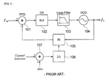
- FIG. 1 is a view schematically showing configuration of a conventional one point PLL direct modulator.
- a conventional PLL direct modulator includes a phase-frequency detector 101 for outputting a synthesized frequency of a reference frequency input through an input terminal and an oscillation frequency from a voltage-controlled oscillator (VCO) 104 which is divided by n by a divider 105 and fed back, a charge pump 102 which receives and pumps the output of the phase-frequency detector 101, a loop-filter 103 which filters the signal passing through the charge pump 102, and the VCO 104 which receives the low-frequency-removed signal by the loop-filter 103 to oscillate a high frequency signal.
- VCO voltage-controlled oscillator
- the conventional one point PLL direct modulator having the above configuration provides a channel (frequency) and data as the input of the divider 105.
- the one point PLL direct modulator there is a problem that the high speed transmission signal is distorted since the input signal (channel) passes through a low pass filter.
- a two point PLL direct modulator is used as shown in FIG. 2 .
- the two point PLL direct modulator provides data as inputs of a divider 205 (having low pass filter characteristics) and a VCO 204 (having high pass filter characteristics). That is, since the data are provided through two paths and form respective loops, distortion of signals can be reduced by complementary compensation of high/low pass characteristics.
- the two point PLL modulator should have a means for reducing a gain mismatch since the frequency gain mismatch in the path into the input of the VCO 204 has great influence on error vector magnitude (EVM).
- EVM error vector magnitude
- the reference numerals 106 and 206, 107 and 207, 201, 202, and 203 represent a sigma-delta modulator, an adder, a phase-frequency detector, a charge pump, and a loop-filter, respectively.
- the present invention has been invented in order to overcome the above-described problems and it is, therefore, an object of the present invention to provide a PLL direct modulator that can reduce a frequency gain mismatch by forming a desired channel frequency using a digital divider and a sigma-delta modulator, changing a division ratio through the sigma-delta modulator, and performing frequency modulation through adjustment of a voltage of a second varactor of a voltage-controlled oscillator (VCO), and a frequency gain mismatch compensation method in the modulator.
- VCO voltage-controlled oscillator
- a PLL direct modulator including: a phase-frequency detector (PFD) for detecting a frequency-phase difference between a reference frequency and a fed-back divided frequency and providing a pulse according to the detected difference; a charge pump (CP) for outputting a plus (+) or minus (-) current pulse by receiving the pulse from the PFD; a loop filter for converting the current pulse from the CP into a voltage; a VCO for outputting a preset frequency signal by receiving the voltage from the loop filter; a divider for dividing the frequency signal from the VCO into a relatively lower frequency signal; and a sigma-delta modulator for outputting an arbitrary numerical value by receiving a specific value, wherein a frequency gain mismatch compensator is installed between the divider and the VCO to modulate the frequency of the VCO by receiving the frequency signal from the divider and modulation data supplied from the outside.
- PFD phase-frequency detector
- CP charge pump
- CP charge pump
- VCO for outputting a preset frequency signal by
- the frequency gain mismatch compensator may include a gain mismatch calibrator for performing calibration for gain mismatch compensation by receiving the frequency signal divided by the divider; and a resistor array stage for modulating the frequency of the VCO by receiving the modulation data supplied from the outside and the output from the gain mismatch calibrator.
- the gain mismatch calibrator may include a divide-by-16 divider for dividing the frequency signal received from a secondary divide-by-2 divider of a first divider by 16 and a digital counter for calculating a counter value of a preset predetermined frequency by receiving the frequency signal divided by the divide-by-16 divider and the reference frequency signal provided from the outside.
- the gain mismatch calibrator may further include an algorithm module for executing an algorithm for gain mismatch calibration based on the counter value of the preset predetermined frequency calculated by the digital counter.
- the resistor array stage may consist of a plurality of resistors connected in series.
- the frequency gain mismatch compensator may modulate the frequency of the VCO by adjusting a voltage of a second varactor of the VCO.
- the divider may include a first divider for dividing the frequency signal from the VCO into the relatively lower frequency signal; and a second divider for forming a desired frequency signal by receiving the output from the first divider and the output value from the sigma-delta modulator.
- the first divider may consist of a primary divide-by-2 divider for dividing the frequency signal from the VCO by 2 into the relatively lower frequency signal, a divide-by-16 divider for dividing the frequency signal divided by 2 by the primary divide-by-2 divider by 16, and a secondary divide-by-2 divider for dividing the frequency signal divided by 16 by the divide-by-16 divider by 2 again.
- the second divider may be a digital multi modulus divider.
- a frequency gain mismatch compensation method in a PLL direct modulator including a frequency gain mismatch compensator, including the steps of: a) calculating a counter value corresponding to a reference frequency by the frequency gain mismatch compensator; b) calculating the current frequency counter value to search a voltage value corresponding to a preset plus frequency by the frequency gain mismatch compensator; c) determining whether a value obtained by subtracting a reference frequency counter value from the current frequency counter value is equal to a preset plus frequency counter value by the frequency gain mismatch compensator; d) storing the voltage value corresponding to the preset plus frequency when the value obtained by subtracting the reference frequency counter value from the current frequency counter value is equal to the preset plus frequency counter value; e) determining whether the value obtained by subtracting the reference frequency counter value from the current frequency counter value is greater than the preset plus frequency counter value and increasing or decreasing a resistor register value according to the result of the determination when the value obtained by
- the resistor register value is increased when the value obtained by subtracting the reference frequency counter value from the current frequency counter value is greater than the preset plus frequency counter value as a result of determining whether the value obtained by subtracting the reference frequency counter value from the current frequency counter value is greater than the preset plus frequency counter value in the step e).
- the resistor register value is decreased when the value obtained by subtracting the reference frequency counter value from the current frequency counter value is less than the preset plus frequency counter value as a result of determining whether the value obtained by subtracting the reference frequency counter value from the current frequency counter value is greater than the preset plus frequency counter value in the step e).
- the resistor register value is increased when the value obtained by subtracting the current frequency counter value from the reference frequency counter value is greater than the preset minus frequency counter value as a result of determining whether the value obtained by subtracting the current frequency counter value from the reference frequency counter value is greater than the preset minus frequency counter value in the step i).
- the resistor register value is decreased when the value obtained by subtracting the current frequency counter value from the reference frequency counter value is less than the preset minus frequency counter value as a result of determining whether the value obtained by subtracting the current frequency counter value from the reference frequency counter value is greater than the preset minus frequency counter value in the step i).
- FIG. 1 is a view schematically showing configuration of a conventional one point PLL direct modulator
- FIG. 2 is a view schematically showing configuration of a conventional two point PLL direct modulator
- FIG. 3 is a view schematically showing configuration of a PLL direct modulator in accordance with an embodiment of the present invention
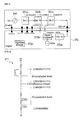
- FIG. 4 is a view showing internal configuration of a gain mismatch calibrator in the PLL direct modulator shown in FIG. 3 ;
- FIG. 5 is a view showing circuit configuration of a resistor array stage in the PLL direct modulator shown in FIG. 3 ;
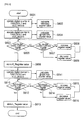
- FIG. 6 is a flowchart showing an execution process of a frequency gain mismatch compensation method in a PLL direct modulator in accordance with the present invention.
- FIG. 3 is a view schematically showing a configuration of a PLL direct modulator in accordance with an embodiment of the present invention.
- a PLL direct modulator in accordance with the present invention includes a phase-frequency detector (PFD) 310, a charge pump (CP) 320, a loop filter 330, a voltage-controlled oscillator (VCO) 340, a divider 350, a sigma-delta modulator 360, and a frequency gain mismatch compensator 370.
- PFD phase-frequency detector
- CP charge pump
- VCO voltage-controlled oscillator
- the PFD 310 detects a frequency-phase difference between a reference frequency and a fed-back divided frequency and provides a pulse according to the detected difference.
- the CP 320 receives the pulse from the PFD 310 to output a plus (+) or minus (-) current pulse.
- the loop filter 330 converts the current pulse from the CP 320 into a voltage.
- the loop filter 330 may be a low pass filter.
- the VCO 340 receives the voltage from the loop filter 330 to output a preset frequency signal.
- the divider 350 divides the frequency signal from the VCO 340 to generate a relatively lower frequency signal.
- the divider 350 may include a first divider 351 which divides the frequency signal from the VCO 340 into a relatively lower frequency signal and a second divider 352 which receives an output from the first divider 351 and an output value from the sigma-delta modulator 360 to form a desired frequency signal.
- the first divider 351 may consist of a primary divide-by-2 divider 351a for dividing the frequency signal from the VCO 340 by 2 to generate a relatively lower frequency signal, a divide-by-16 divider for dividing the frequency signal, which is divided by 2 by the primary divide-by-2 divider 351a, by 16, and a secondary divide-by-2 divider 351c for dividing the frequency signal, which is divided by 16 by the divide-by-16 divider 351b, by 2 again.
- the second divider 352 may be a digital multi modulus divider.
- the sigma-delta modulator 360 has a function of continuously outputting a varying arbitrary numerical value by receiving a specific value (for example, a specific integer value).
- the frequency gain mismatch compensator 370 is installed between the divider 350 and the VCO 340 and modulates the frequency of the VCO 340 by receiving the frequency signal from the divider 350 and modulation data Mod ( ⁇ K) from the outside.
- the frequency gain mismatch compensator 370 may include a resistor array stage 371 and a gain mismatch calibrator 372.
- the resistor array stage 371 modulates the frequency of the VCO 340 by receiving the modulation data Mod ( ⁇ K) from the outside and an output from the gain mismatch calibrator 372. At this time, the resistor array stage 371 may consist of a plurality of resistors connected in series as shown in FIG. 5 .
- the gain mismatch calibrator 372 performs calibration for gain mismatch compensation by receiving the frequency signal divided by the divider 350.
- the gain mismatch calibrator 372 may include a divide-by-16 divider 372a which divides the frequency signal received from the secondary divide-by-2 divider 351c of the first divider 351 by 16 and a digital counter 372b which counts a counter value of a preset predetermined frequency by receiving the frequency signal divided by the divide-by-16 divider 372a and the reference frequency signal provided from the outside.
- the gain mismatch calibrator 372 may further include an algorithm module 372c which executes an algorithm for gain mismatch calibration based on the counter value of the preset predetermined frequency calculated by the digital counter 372b.
- the frequency gain mismatch compensator 370 may modulate the frequency of the VCO 340 by adjusting a voltage of a second varactor of the VCO 340. That is, the frequency gain mismatch compensator 370 calculates a counter value of 500 kHz, for example, using a digital counter 352b of 32 MHz. Further, the frequency gain mismatch compensator 370 searches the current frequency counter value by receiving the data Mod ( ⁇ K) signal provided from the outside, searches a varactor application voltage of 500 kHz by comparing the current frequency counter value with the counter value of 500 kHz and changing a control signal of the resistor array stage 371, and modulates the frequency of the VCO 340 based on it.
- ⁇ K data Mod
- Vc and Vs represent a first varactor input voltage and a second varactor input voltage, respectively.
- FIG. 6 is a flowchart showing an execution process of a frequency gain mismatch compensation method in a PLL direct modulator in accordance with the present invention.
- the frequency gain mismatch compensation method in a PLL direct modulator in accordance with the present invention is a frequency gain mismatch compensation method in the above-described PLL direct modulator including a PFD 310, a CP 320, a loop filter 330, a VCO 340, a divider 350, a sigma-delta modulator 360, and a frequency gain mismatch compensator 370.
- a counter value corresponding to a reference frequency is calculated by the frequency gain mismatch compensator 370 (S601 and S602).
- the PLL direct modulator of the present invention is changed into an open loop, and an arbitrary control voltage is applied to the PLL modulator to be used as an input voltage of a first varactor of the VCO 340.
- the counter value corresponding to the reference frequency is calculated after operating a digital counter 372b in a state in which register stages "TXMODEN” and “VCO_MOD” (refer to FIG. 4 ) of a gain mismatch calibrator 372 are set to 1 and 0, respectively.
- the current frequency counter value is calculated similarly by the frequency gain mismatch compensator 370 to search a voltage value corresponding to a preset plus frequency (for example, +500 kHz) (S603 and S604). That is, the current frequency counter value is calculated after operating the digital counter 372b in a state in which the register stages "TXMODEN” and “VCO_MOD" of the gain mismatch calibrator 372 are set to 1 and 0, respectively.
- the frequency gain mismatch compensator 370 determines whether a value obtained by subtracting a reference frequency counter value from the current frequency counter value is equal to a preset plus frequency counter value (S605).
- the voltage value corresponding to the preset plus frequency is stored in a register H_Register (S606).
- the resistor register value is increased (S608).
- the resistor register value is decreased (S609).
- the current frequency counter value is calculated by the frequency gain mismatch compensator 370 to search a voltage value corresponding to a preset minus frequency (for example, -500 kHz) (S610 and S611). That is, the current frequency counter value is calculated to search the voltage value corresponding to the preset minus frequency after operating the digital counter 372b in a state in which the register stages "TXMODEN” and "VCO_MOD" of the gain mismatch compensator 372 are all set to 0.
- a preset minus frequency for example, -500 kHz
- the frequency gain mismatch compensator 370 determines whether a value obtained by subtracting the current frequency counter value from the reference frequency counter value is equal to a preset minus frequency counter value (S612).
- the voltage value corresponding to the preset minus frequency is stored in a register L_Register (S613).
- the resistor register value is increased (S615).
- the resistor register value is decreased (S616).
- the PLL direct modulator in accordance with the present invention can reduce a frequency gain mismatch in a PLL modulator by forming a desired channel frequency using a digital divider and a sigma-delta modulator, compensating the frequency gain mismatch through a frequency gain mismatch compensator, and performing frequency modulation through adjustment of a voltage of a second varactor of a VCO.
Landscapes
- Stabilization Of Oscillater, Synchronisation, Frequency Synthesizers (AREA)
Abstract
The present invention relates to a PLL direct modulator and a frequency gain mismatch compensation method in the modulator.
A PLL direct modulator in accordance with the present invention includes: a phase-frequency detector (PFD), a charge pump (CP), a loop filter, a voltage-controlled oscillator (VCO), a divider, and a sigma-delta modulator, wherein a frequency gain mismatch compensator is installed between the divider and the VCO to modulate a frequency of the VCO by receiving a frequency signal from the divider and modulation data supplied from the outside.
According to the present invention, it is possible to reduce a frequency gain mismatch in the PLL modulator by compensating the frequency gain mismatch through the frequency gain mismatch compensator.
Description
- Claim and incorporate by reference domestic priority application and foreign priority application as follows:
- This application claims the foreign priority benefit of Korean Patent Application No.
10-2013-0044225 - The present invention relates to a phase-locked loop (PLL) direct modulator, and more particularly, to a PLL direct modulator that can reduce a frequency gain mismatch by changing a division ratio through a sigma-delta modulator and compensating the frequency gain mismatch through a frequency gain mismatch compensator, and a frequency gain mismatch compensation method in the modulator.
- In recent times, as a minimum line width is reduced to less than tens of nm with the day-to-day development of semiconductor technologies, competiveness of semiconductor chips depend on a chip area. Therefore, in the communication chip market, structures for reducing a chip area have been continuously disclosed in recent years. Among them, a PLL director modulator structure, which is a structure capable of removing a mixer and a digital-to-analog (D/A) converter of a transmitter, has received much attention recently. The biggest advantage of the PLL direct modulator is that it can reduce an area, and the disadvantage thereof is that a high-speed transmission signal is distorted due to characteristics of a PLL low pass filter since data is sent to a PLL loop as an input.
-
FIG. 1 is a view schematically showing configuration of a conventional one point PLL direct modulator. - Referring to
FIG. 1 , a conventional PLL direct modulator includes a phase-frequency detector 101 for outputting a synthesized frequency of a reference frequency input through an input terminal and an oscillation frequency from a voltage-controlled oscillator (VCO) 104 which is divided by n by adivider 105 and fed back, acharge pump 102 which receives and pumps the output of the phase-frequency detector 101, a loop-filter 103 which filters the signal passing through thecharge pump 102, and theVCO 104 which receives the low-frequency-removed signal by the loop-filter 103 to oscillate a high frequency signal. - The conventional one point PLL direct modulator having the above configuration provides a channel (frequency) and data as the input of the
divider 105. However, in the one point PLL direct modulator, there is a problem that the high speed transmission signal is distorted since the input signal (channel) passes through a low pass filter. - In order to prevent the distortion of the high speed transmission signal, in the prior art, a two point PLL direct modulator is used as shown in
FIG. 2 . - The two point PLL direct modulator provides data as inputs of a divider 205 (having low pass filter characteristics) and a VCO 204 (having high pass filter characteristics). That is, since the data are provided through two paths and form respective loops, distortion of signals can be reduced by complementary compensation of high/low pass characteristics.
- However, the two point PLL modulator should have a means for reducing a gain mismatch since the frequency gain mismatch in the path into the input of the
VCO 204 has great influence on error vector magnitude (EVM). InFIGS. 1 and2 , thereference numerals -
- Patent Document 1: Japanese Patent Laid-open Publication No.
2011-509047 - Patent Document 2: U.S. Patent Laid-open Publication No.
US2007-0109067 - The present invention has been invented in order to overcome the above-described problems and it is, therefore, an object of the present invention to provide a PLL direct modulator that can reduce a frequency gain mismatch by forming a desired channel frequency using a digital divider and a sigma-delta modulator, changing a division ratio through the sigma-delta modulator, and performing frequency modulation through adjustment of a voltage of a second varactor of a voltage-controlled oscillator (VCO), and a frequency gain mismatch compensation method in the modulator.
- In accordance with one aspect of the present invention to achieve the object, there is provided a PLL direct modulator including: a phase-frequency detector (PFD) for detecting a frequency-phase difference between a reference frequency and a fed-back divided frequency and providing a pulse according to the detected difference; a charge pump (CP) for outputting a plus (+) or minus (-) current pulse by receiving the pulse from the PFD; a loop filter for converting the current pulse from the CP into a voltage; a VCO for outputting a preset frequency signal by receiving the voltage from the loop filter; a divider for dividing the frequency signal from the VCO into a relatively lower frequency signal; and a sigma-delta modulator for outputting an arbitrary numerical value by receiving a specific value, wherein a frequency gain mismatch compensator is installed between the divider and the VCO to modulate the frequency of the VCO by receiving the frequency signal from the divider and modulation data supplied from the outside.
- Here, the frequency gain mismatch compensator may include a gain mismatch calibrator for performing calibration for gain mismatch compensation by receiving the frequency signal divided by the divider; and a resistor array stage for modulating the frequency of the VCO by receiving the modulation data supplied from the outside and the output from the gain mismatch calibrator.
- At this time, the gain mismatch calibrator may include a divide-by-16 divider for dividing the frequency signal received from a secondary divide-by-2 divider of a first divider by 16 and a digital counter for calculating a counter value of a preset predetermined frequency by receiving the frequency signal divided by the divide-by-16 divider and the reference frequency signal provided from the outside.
- At this time, the gain mismatch calibrator may further include an algorithm module for executing an algorithm for gain mismatch calibration based on the counter value of the preset predetermined frequency calculated by the digital counter.
- Further, the resistor array stage may consist of a plurality of resistors connected in series.
- Further, the frequency gain mismatch compensator may modulate the frequency of the VCO by adjusting a voltage of a second varactor of the VCO.
- Further, the divider may include a first divider for dividing the frequency signal from the VCO into the relatively lower frequency signal; and a second divider for forming a desired frequency signal by receiving the output from the first divider and the output value from the sigma-delta modulator.
- At this time, the first divider may consist of a primary divide-by-2 divider for dividing the frequency signal from the VCO by 2 into the relatively lower frequency signal, a divide-by-16 divider for dividing the frequency signal divided by 2 by the primary divide-by-2 divider by 16, and a secondary divide-by-2 divider for dividing the frequency signal divided by 16 by the divide-by-16 divider by 2 again.
- Further, the second divider may be a digital multi modulus divider.
- Further, in accordance with another aspect of the present invention to achieve the object, there is provided a frequency gain mismatch compensation method in a PLL direct modulator including a frequency gain mismatch compensator, including the steps of: a) calculating a counter value corresponding to a reference frequency by the frequency gain mismatch compensator; b) calculating the current frequency counter value to search a voltage value corresponding to a preset plus frequency by the frequency gain mismatch compensator; c) determining whether a value obtained by subtracting a reference frequency counter value from the current frequency counter value is equal to a preset plus frequency counter value by the frequency gain mismatch compensator; d) storing the voltage value corresponding to the preset plus frequency when the value obtained by subtracting the reference frequency counter value from the current frequency counter value is equal to the preset plus frequency counter value; e) determining whether the value obtained by subtracting the reference frequency counter value from the current frequency counter value is greater than the preset plus frequency counter value and increasing or decreasing a resistor register value according to the result of the determination when the value obtained by subtracting the reference frequency counter value from the current frequency counter value is not equal to the preset plus frequency counter value; f) calculating the current frequency counter value to search a voltage value corresponding to a preset minus frequency by the frequency gain mismatch compensator; g) determining whether a value obtained by subtracting the current frequency counter value from the reference frequency counter value is equal to a preset minus frequency counter value by the frequency gain mismatch compensator; h) storing the voltage value corresponding to the preset minus frequency when the value obtained by subtracting the current frequency counter value from the reference frequency counter value is equal to the preset minus frequency counter value; and i) determining whether the value obtained by subtracting the current frequency counter value from the reference frequency counter value is greater than the preset minus frequency counter value and increasing or decreasing the resistor register value according to the result of the determination when the value obtained by subtracting the current frequency counter value from the reference frequency counter value is not equal to the preset minus frequency counter value.
- Here, the resistor register value is increased when the value obtained by subtracting the reference frequency counter value from the current frequency counter value is greater than the preset plus frequency counter value as a result of determining whether the value obtained by subtracting the reference frequency counter value from the current frequency counter value is greater than the preset plus frequency counter value in the step e).
- Further, the resistor register value is decreased when the value obtained by subtracting the reference frequency counter value from the current frequency counter value is less than the preset plus frequency counter value as a result of determining whether the value obtained by subtracting the reference frequency counter value from the current frequency counter value is greater than the preset plus frequency counter value in the step e).
- Further, the resistor register value is increased when the value obtained by subtracting the current frequency counter value from the reference frequency counter value is greater than the preset minus frequency counter value as a result of determining whether the value obtained by subtracting the current frequency counter value from the reference frequency counter value is greater than the preset minus frequency counter value in the step i).
- Further, the resistor register value is decreased when the value obtained by subtracting the current frequency counter value from the reference frequency counter value is less than the preset minus frequency counter value as a result of determining whether the value obtained by subtracting the current frequency counter value from the reference frequency counter value is greater than the preset minus frequency counter value in the step i).
- These and/or other aspects and advantages of the present general inventive concept will become apparent and more readily appreciated from the following description of the embodiments, taken in conjunction with the accompanying drawings of which:
-
FIG. 1 is a view schematically showing configuration of a conventional one point PLL direct modulator; -
FIG. 2 is a view schematically showing configuration of a conventional two point PLL direct modulator; -
FIG. 3 is a view schematically showing configuration of a PLL direct modulator in accordance with an embodiment of the present invention; -
FIG. 4 is a view showing internal configuration of a gain mismatch calibrator in the PLL direct modulator shown inFIG. 3 ; -
FIG. 5 is a view showing circuit configuration of a resistor array stage in the PLL direct modulator shown inFIG. 3 ; and -
FIG. 6 is a flowchart showing an execution process of a frequency gain mismatch compensation method in a PLL direct modulator in accordance with the present invention. - The terms or words used in the present specification and claims should not be interpreted as being limited to typical or dictionary meanings, but should be interpreted as having meanings and concepts relevant to the technical spirit of the present invention based on the rule according to which an inventor can appropriately define the concept of the term to describe his/her own invention in the best manner.
- Throughout the specification, when an element is referred to as "including" another element, it can further include the other element rather than exclude the other element unless the context clearly indicates otherwise. Further, the terms "unit", "module", "apparatus", etc. used in the present specification represent a unit for processing at least one function or operation and may be implemented by hardware, software, or a combination thereof.
- Hereinafter, embodiments of the present invention will be described in detail with reference to the accompanying drawings.
-
FIG. 3 is a view schematically showing a configuration of a PLL direct modulator in accordance with an embodiment of the present invention. - Referring to
FIG. 3 , a PLL direct modulator in accordance with the present invention includes a phase-frequency detector (PFD) 310, a charge pump (CP) 320, aloop filter 330, a voltage-controlled oscillator (VCO) 340, adivider 350, a sigma-delta modulator 360, and a frequencygain mismatch compensator 370. - The
PFD 310 detects a frequency-phase difference between a reference frequency and a fed-back divided frequency and provides a pulse according to the detected difference. - The
CP 320 receives the pulse from thePFD 310 to output a plus (+) or minus (-) current pulse. - The
loop filter 330 converts the current pulse from theCP 320 into a voltage. Here, theloop filter 330 may be a low pass filter. - The
VCO 340 receives the voltage from theloop filter 330 to output a preset frequency signal. - The
divider 350 divides the frequency signal from theVCO 340 to generate a relatively lower frequency signal. Here, thedivider 350 may include afirst divider 351 which divides the frequency signal from theVCO 340 into a relatively lower frequency signal and asecond divider 352 which receives an output from thefirst divider 351 and an output value from the sigma-delta modulator 360 to form a desired frequency signal. - At this time, the
first divider 351 may consist of a primary divide-by-2divider 351a for dividing the frequency signal from theVCO 340 by 2 to generate a relatively lower frequency signal, a divide-by-16 divider for dividing the frequency signal, which is divided by 2 by the primary divide-by-2divider 351a, by 16, and a secondary divide-by-2divider 351c for dividing the frequency signal, which is divided by 16 by the divide-by-16divider 351b, by 2 again. - Further, the
second divider 352 may be a digital multi modulus divider. - The sigma-
delta modulator 360 has a function of continuously outputting a varying arbitrary numerical value by receiving a specific value (for example, a specific integer value). - The frequency
gain mismatch compensator 370 is installed between thedivider 350 and theVCO 340 and modulates the frequency of theVCO 340 by receiving the frequency signal from thedivider 350 and modulation data Mod (ΔK) from the outside. - Here, the frequency
gain mismatch compensator 370 may include aresistor array stage 371 and again mismatch calibrator 372. - The
resistor array stage 371 modulates the frequency of theVCO 340 by receiving the modulation data Mod (ΔK) from the outside and an output from thegain mismatch calibrator 372. At this time, theresistor array stage 371 may consist of a plurality of resistors connected in series as shown inFIG. 5 . - The
gain mismatch calibrator 372 performs calibration for gain mismatch compensation by receiving the frequency signal divided by thedivider 350. - At this time, the
gain mismatch calibrator 372 may include a divide-by-16divider 372a which divides the frequency signal received from the secondary divide-by-2divider 351c of thefirst divider 351 by 16 and a digital counter 372b which counts a counter value of a preset predetermined frequency by receiving the frequency signal divided by the divide-by-16divider 372a and the reference frequency signal provided from the outside. - At this time, further, the
gain mismatch calibrator 372 may further include analgorithm module 372c which executes an algorithm for gain mismatch calibration based on the counter value of the preset predetermined frequency calculated by the digital counter 372b. - Further, the frequency
gain mismatch compensator 370 may modulate the frequency of theVCO 340 by adjusting a voltage of a second varactor of theVCO 340. That is, the frequencygain mismatch compensator 370 calculates a counter value of 500 kHz, for example, using a digital counter 352b of 32 MHz. Further, the frequencygain mismatch compensator 370 searches the current frequency counter value by receiving the data Mod (ΔK) signal provided from the outside, searches a varactor application voltage of 500 kHz by comparing the current frequency counter value with the counter value of 500 kHz and changing a control signal of theresistor array stage 371, and modulates the frequency of theVCO 340 based on it. - In
FIG. 3 , the reference numerals "Vc" and "Vs" represent a first varactor input voltage and a second varactor input voltage, respectively. - Then, a frequency gain mismatch compensation method in the PLL direct modulator in accordance with the present invention having the above configuration will be described.
-
FIG. 6 is a flowchart showing an execution process of a frequency gain mismatch compensation method in a PLL direct modulator in accordance with the present invention. - Referring to
FIG. 6 , the frequency gain mismatch compensation method in a PLL direct modulator in accordance with the present invention is a frequency gain mismatch compensation method in the above-described PLL direct modulator including aPFD 310, aCP 320, aloop filter 330, aVCO 340, adivider 350, a sigma-delta modulator 360, and a frequencygain mismatch compensator 370. First, a counter value corresponding to a reference frequency is calculated by the frequency gain mismatch compensator 370 (S601 and S602). That is, first of all, the PLL direct modulator of the present invention is changed into an open loop, and an arbitrary control voltage is applied to the PLL modulator to be used as an input voltage of a first varactor of theVCO 340. After that, the counter value corresponding to the reference frequency is calculated after operating a digital counter 372b in a state in which register stages "TXMODEN" and "VCO_MOD" (refer toFIG. 4 ) of again mismatch calibrator 372 are set to 1 and 0, respectively. - When the calculation of the counter value corresponding to the reference frequency is completed in this way, the current frequency counter value is calculated similarly by the frequency
gain mismatch compensator 370 to search a voltage value corresponding to a preset plus frequency (for example, +500 kHz) (S603 and S604). That is, the current frequency counter value is calculated after operating the digital counter 372b in a state in which the register stages "TXMODEN" and "VCO_MOD" of thegain mismatch calibrator 372 are set to 1 and 0, respectively. - When the calculation of the current frequency counter value is completed by the above process, the frequency
gain mismatch compensator 370 determines whether a value obtained by subtracting a reference frequency counter value from the current frequency counter value is equal to a preset plus frequency counter value (S605). - When the value obtained by subtracting the reference frequency counter value from the current frequency counter value is equal to the preset plus frequency counter value in the determination of the step S605, the voltage value corresponding to the preset plus frequency is stored in a register H_Register (S606).
- And, when the value obtained by subtracting the reference frequency counter value from the current frequency counter value isn't equal to the preset plus frequency counter value in the determination of the step S605, it is determined whether the value obtained by subtracting the reference frequency counter value from the current frequency counter value is greater than the preset plus frequency counter value (S607), and a resistor register value is increased or decreased according to the result of the determination.
- That is, when the value obtained by subtracting the reference frequency counter value from the current frequency counter value is greater than the preset plus frequency counter value as a result of determining whether the value obtained by subtracting the reference frequency counter value from the current frequency counter value is greater than the preset plus frequency counter value, the resistor register value is increased (S608).
- And, when the value obtained by subtracting the reference frequency counter value from the current frequency counter value is less than the preset plus frequency counter value as a result of determining whether the value obtained by subtracting the reference frequency counter value from the current frequency counter value is greater than the preset plus frequency counter value, the resistor register value is decreased (S609).
- After that, the current frequency counter value is calculated by the frequency
gain mismatch compensator 370 to search a voltage value corresponding to a preset minus frequency (for example, -500 kHz) (S610 and S611). That is, the current frequency counter value is calculated to search the voltage value corresponding to the preset minus frequency after operating the digital counter 372b in a state in which the register stages "TXMODEN" and "VCO_MOD" of thegain mismatch compensator 372 are all set to 0. - When the calculation of the current frequency counter value is completed in the step S611, the frequency
gain mismatch compensator 370 determines whether a value obtained by subtracting the current frequency counter value from the reference frequency counter value is equal to a preset minus frequency counter value (S612). - When the value obtained by subtracting the current frequency counter value from the reference frequency counter value is equal to the preset minus frequency counter value in the determination of the step S612, the voltage value corresponding to the preset minus frequency is stored in a register L_Register (S613).
- And, when the value obtained by subtracting the current frequency counter value from the reference frequency counter value isn't equal to the preset minus frequency counter value in the determination of the step S612, it is determined whether the value obtained by subtracting the current frequency counter value from the reference frequency counter value is greater than the preset minus frequency counter value (S614), and the resistor register value is increased or decreased according to the result of the determination.
- That is, when the value obtained by subtracting the current frequency counter value from the reference frequency counter value is greater than the preset minus frequency counter value as a result of determining whether the value obtained by subtracting the current frequency counter value from the reference frequency counter value is greater than the preset minus frequency counter value in the step S614, the resistor register value is increased (S615).
- And, when the value obtained by subtracting the current frequency counter value from the reference frequency counter value is less than the preset minus frequency counter value as a result of determining whether the value obtained by subtracting the current frequency counter value from the reference frequency counter value is greater than the preset minus frequency counter value in the step S614, the resistor register value is decreased (S616).
- Like the above, it is possible to modulate the frequency of the
VCO 340 by searching the current frequency counter value, comparing the current frequency counter value with the counter value of the preset predetermined frequency (500 kHz), and searching the varactor application voltage of theVCO 340 through increase or decrease in resistance of theresistor array stage 371, thereby compensating a frequency gain mismatch. - As in the above description, the PLL direct modulator in accordance with the present invention can reduce a frequency gain mismatch in a PLL modulator by forming a desired channel frequency using a digital divider and a sigma-delta modulator, compensating the frequency gain mismatch through a frequency gain mismatch compensator, and performing frequency modulation through adjustment of a voltage of a second varactor of a VCO.
- Although the preferable embodiments of the present invention have been described in detail above, the present invention is not limited to the embodiments and it will be appreciated by those skilled in the art that various modifications and applications may be made in the embodiments without departing from the technical spirit of the present invention. Therefore, the range of protection of the present invention should be interpreted from the appended claims and all technical sprits within the range equivalent to the range should be interpreted as being included in the range of the rights of the present invention.
Claims (14)
- A PLL direct modulator comprising:a phase-frequency detector (PFD) for detecting a frequency-phase difference between a reference frequency and a fed-back divided frequency and providing a pulse according to the detected difference;a charge pump (CP) for outputting a plus (+) or minus (-) current pulse by receiving the pulse from the PFD;a loop filter for converting the current pulse from the CP into a voltage;a voltage-controlled oscillator (VCO) for outputting a preset frequency signal by receiving the voltage from the loop filter;a divider for dividing the frequency signal from the VCO into a relatively lower frequency signal; anda sigma-delta modulator for outputting an arbitrary numerical value by receiving a specific value, wherein a frequency gain mismatch compensator is installed between the divider and the VCO to modulate the frequency of the VCO by receiving the frequency signal from the divider and modulation data supplied from the outside.
- The PLL direct modulator according to claim 1, wherein the frequency gain mismatch compensator comprises:a gain mismatch calibrator for performing calibration for gain mismatch compensation by receiving the frequency signal divided by the divider; anda resistor array stage for modulating the frequency of the VCO by receiving the modulation data supplied from the outside and the output from the gain mismatch calibrator.
- The PLL direct modulator according to claim 2, wherein the gain mismatch calibrator comprises:a divide-by-16 divider for dividing the frequency signal received from a secondary divide-by-2 divider of a first divider by 16; anda digital counter for calculating a counter value of a preset predetermined frequency by receiving the frequency signal divided by the divide-by-16 divider and the reference frequency signal provided from the outside.
- The PLL direct modulator according to claim 3, wherein the gain mismatch calibrator further comprises an algorithm module for executing an algorithm for gain mismatch calibration based on the counter value of the preset predetermined frequency calculated by the digital counter.
- The PLL direct modulator according to claim 2, wherein the resistor array stage consists of a plurality of resistors connected in series.
- The PLL direct modulator according to claim 1, wherein the frequency gain mismatch compensator modulates the frequency of the VCO by adjusting a voltage of a second varactor of the VCO.
- The PLL direct modulator according to claim 1, wherein the divider comprises:a first divider for dividing the frequency signal from the VCO into a relatively lower frequency signal; anda second divider for forming a desired frequency signal by receiving the output from the first divider and the output value from the sigma-delta modulator.
- The PLL direct modulator according to claim 7, wherein the first divider consists of a primary divide-by-2 divider for dividing the frequency signal from the VCO by 2 into a relatively lower frequency signal, a divide-by-16 divider for dividing the frequency signal divided by 2 by the primary divide-by-2 divider by 16, and a secondary divide-by-2 divider for dividing the frequency signal divided by 16 by the divide-by-16 divider by 2 again.
- The PLL direct modulator according to claim 7, wherein the second divider is a digital multi modulus divider.
- A frequency gain mismatch compensation method in a PLL direct modulator comprising a frequency gain mismatch compensator, comprising:a) calculating a counter value corresponding to a reference frequency by the frequency gain mismatch compensator;b) calculating the current frequency counter value to search a voltage value corresponding to a preset plus frequency by the frequency gain mismatch compensator;c) determining whether a value obtained by subtracting a reference frequency counter value from the current frequency counter value is equal to a preset plus frequency counter value by the frequency gain mismatch compensator;d) storing the voltage value corresponding to the preset plus frequency when the value obtained by subtracting the reference frequency counter value from the current frequency counter value is equal to the preset plus frequency counter value;e) determining whether the value obtained by subtracting the reference frequency counter value from the current frequency counter value is greater than the preset plus frequency counter value and increasing or decreasing a resistor register value according to the result of the determination when the value obtained by subtracting the reference frequency counter value from the current frequency counter value is not equal to the preset plus frequency counter value;f) calculating the current frequency counter value to search a voltage value
corresponding to a preset minus frequency by the frequency gain mismatch compensator;g) determining whether a value obtained by subtracting the current frequency counter value from the reference frequency counter value is equal to a preset minus frequency counter value by the frequency gain mismatch compensator;h) storing the voltage value corresponding to the preset minus frequency when the value obtained by subtracting the current frequency counter value from the reference frequency counter value is equal to the preset minus frequency counter value; andi) determining whether the value obtained by subtracting the current frequency counter value from the reference frequency counter value is greater than the preset minus frequency counter value and increasing or decreasing the resistor register value according to the result of the determination when the value obtained by subtracting the current frequency counter value from the reference frequency counter value is not equal to the preset minus frequency counter value. - The frequency gain mismatch compensation method according to claim 10, wherein the resistor register value is increased when the value obtained by subtracting the reference frequency counter value from the current frequency counter value is greater than the preset plus frequency counter value as a result of determining whether the value obtained by subtracting the reference frequency counter value from the current frequency counter value is greater than the preset plus frequency counter value in the step e).
- The frequency gain mismatch compensation method according to claim 10,
wherein the resistor register value is decreased when the value obtained by subtracting the reference frequency counter value from the current frequency counter value is less than the preset plus frequency counter value as a result of determining whether the value obtained by subtracting the reference frequency counter value from the current frequency counter value is greater than the preset plus frequency counter value in the step e). - The frequency gain mismatch compensation method according to claim 10, wherein the resistor register value is increased when the value obtained by subtracting the current frequency counter value from the reference frequency counter value is greater than the preset minus frequency counter value as a result of determining whether the value obtained by subtracting the current frequency counter value from the reference frequency counter value is greater than the preset minus frequency counter value in the step i).
- The frequency gain mismatch compensation method according to claim 10, wherein the resistor register value is decreased when the value obtained by subtracting the current frequency counter value from the reference frequency counter value is less than the preset minus frequency counter value as a result of determining whether the value obtained by subtracting the current frequency counter value from the reference frequency counter value is greater than the preset minus frequency counter value in the step i).
Applications Claiming Priority (1)
| Application Number | Priority Date | Filing Date | Title |
|---|---|---|---|
| KR20130044225A KR101483855B1 (en) | 2013-04-22 | 2013-04-22 | PLL(Phase-Locked Loop) direct modulator and frequency gain mismatch compensation method in the modulator |
Publications (1)
| Publication Number | Publication Date |
|---|---|
| EP2797224A1 true EP2797224A1 (en) | 2014-10-29 |
Family
ID=49510087
Family Applications (1)
| Application Number | Title | Priority Date | Filing Date |
|---|---|---|---|
| EP13275271.8A Withdrawn EP2797224A1 (en) | 2013-04-22 | 2013-10-29 | PLL direct modulator and frequency gain mismatch compensation method in the modulator |
Country Status (2)
| Country | Link |
|---|---|
| EP (1) | EP2797224A1 (en) |
| KR (1) | KR101483855B1 (en) |
Families Citing this family (2)
| Publication number | Priority date | Publication date | Assignee | Title |
|---|---|---|---|---|
| EP4064569A1 (en) | 2021-03-23 | 2022-09-28 | Nxp B.V. | Type-i plls for phase-controlled applications |
| EP4064568B1 (en) | 2021-03-23 | 2025-05-07 | Nxp B.V. | Type-i plls for phase-controlled applications |
Citations (4)
| Publication number | Priority date | Publication date | Assignee | Title |
|---|---|---|---|---|
| US20070109067A1 (en) | 2005-11-17 | 2007-05-17 | O'sullivan Cormac E | Phase lock loop RF modulator system |
| US20090153254A1 (en) * | 2007-11-05 | 2009-06-18 | Hwa Yeal Yu | Phase locked loop circuit performing two point modulation and gain calibration method thereof |
| US20090174492A1 (en) * | 2008-01-04 | 2009-07-09 | Qualcomm Incorporated | Phase-locked loop with self-correcting phase-to-digital transfer function |
| US20120212296A1 (en) * | 2011-02-17 | 2012-08-23 | Hsin-Hung Chen | Signal generating circuit and signal generating method |
Family Cites Families (2)
| Publication number | Priority date | Publication date | Assignee | Title |
|---|---|---|---|---|
| US6140883A (en) | 1997-10-17 | 2000-10-31 | Intel Corporation | Tunable, energy efficient clocking scheme |
| KR100847687B1 (en) * | 2006-10-20 | 2008-07-23 | (주)에프씨아이 | Frequency Synthesizer and Frequency Control Method |
-
2013
- 2013-04-22 KR KR20130044225A patent/KR101483855B1/en not_active Expired - Fee Related
- 2013-10-29 EP EP13275271.8A patent/EP2797224A1/en not_active Withdrawn
Patent Citations (5)
| Publication number | Priority date | Publication date | Assignee | Title |
|---|---|---|---|---|
| US20070109067A1 (en) | 2005-11-17 | 2007-05-17 | O'sullivan Cormac E | Phase lock loop RF modulator system |
| US20090153254A1 (en) * | 2007-11-05 | 2009-06-18 | Hwa Yeal Yu | Phase locked loop circuit performing two point modulation and gain calibration method thereof |
| US20090174492A1 (en) * | 2008-01-04 | 2009-07-09 | Qualcomm Incorporated | Phase-locked loop with self-correcting phase-to-digital transfer function |
| JP2011509047A (en) | 2008-01-04 | 2011-03-17 | クゥアルコム・インコーポレイテッド | Phase-locked loop with self-correcting phase digital transfer function |
| US20120212296A1 (en) * | 2011-02-17 | 2012-08-23 | Hsin-Hung Chen | Signal generating circuit and signal generating method |
Also Published As
| Publication number | Publication date |
|---|---|
| KR20140126106A (en) | 2014-10-30 |
| KR101483855B1 (en) | 2015-01-16 |
Similar Documents
| Publication | Publication Date | Title |
|---|---|---|
| KR101579663B1 (en) | Apparatus and methods for adjusting voltage controlled oscillator gain | |
| US8098110B2 (en) | Phase locked loop apparatus with selectable capacitance device | |
| US8487707B2 (en) | Frequency synthesizer | |
| KR100682279B1 (en) | Adaptive frequency regulator of frequency synthesizer | |
| US7907022B2 (en) | Phase-locked loop and method for operating the same | |
| US8427243B2 (en) | Signal generating circuit and signal generating method | |
| US7948286B2 (en) | Bandwidth control apparatus for phase lock loop and method thereof | |
| CN107707254B (en) | Apparatus and method for calibrating the frequency of an oscillator in response to an external signal | |
| US6914489B2 (en) | Voltage-controlled oscillator presetting circuit | |
| US9722617B2 (en) | Phase locked loop and associated method for loop gain calibration | |
| US9350296B1 (en) | Systems and methods for calibrating a dual port phase locked loop | |
| US20080246521A1 (en) | Multiple reference frequency fractional-n pll (phase locked loop) | |
| EP2232709A1 (en) | Systems and methods for calibrating the loop bandwidth of a phase-locked loop (pll) | |
| US10218367B2 (en) | Frequency synthesizing device and automatic calibration method thereof | |
| JP5367075B2 (en) | PLL frequency synthesizer | |
| US10715158B1 (en) | Phase-locked loop (PLL) with calibration circuit | |
| US20150130544A1 (en) | Method and apparatus to calibrate frequency synthesizer | |
| US20080036544A1 (en) | Method for adjusting oscillator in phase-locked loop and related frequency synthesizer | |
| US8258833B2 (en) | Phase locked loop circuits | |
| KR101483855B1 (en) | PLL(Phase-Locked Loop) direct modulator and frequency gain mismatch compensation method in the modulator | |
| US20090224842A1 (en) | Phase lock loop apparatus | |
| US10536153B1 (en) | Signal generator | |
| KR20180131017A (en) | Frequency Synthesizer with Dual Paths for Wideband FMCW | |
| KR101007391B1 (en) | Apparatus and method for improving phase noise in phase locked loops | |
| US11290118B2 (en) | Frequency synthesizer |
Legal Events
| Date | Code | Title | Description |
|---|---|---|---|
| PUAI | Public reference made under article 153(3) epc to a published international application that has entered the european phase |
Free format text: ORIGINAL CODE: 0009012 |
|
| 17P | Request for examination filed |
Effective date: 20131029 |
|
| AK | Designated contracting states |
Kind code of ref document: A1 Designated state(s): AL AT BE BG CH CY CZ DE DK EE ES FI FR GB GR HR HU IE IS IT LI LT LU LV MC MK MT NL NO PL PT RO RS SE SI SK SM TR |
|
| AX | Request for extension of the european patent |
Extension state: BA ME |
|
| STAA | Information on the status of an ep patent application or granted ep patent |
Free format text: STATUS: THE APPLICATION HAS BEEN WITHDRAWN |
|
| 18W | Application withdrawn |
Effective date: 20151118 |