EP2797135A2 - Organic Light-Emitting Display Device and Method of Manufacturing the Same - Google Patents
Organic Light-Emitting Display Device and Method of Manufacturing the Same Download PDFInfo
- Publication number
- EP2797135A2 EP2797135A2 EP14155647.2A EP14155647A EP2797135A2 EP 2797135 A2 EP2797135 A2 EP 2797135A2 EP 14155647 A EP14155647 A EP 14155647A EP 2797135 A2 EP2797135 A2 EP 2797135A2
- Authority
- EP
- European Patent Office
- Prior art keywords
- organic light
- film
- elastic layer
- inorganic
- display device
- Prior art date
- Legal status (The legal status is an assumption and is not a legal conclusion. Google has not performed a legal analysis and makes no representation as to the accuracy of the status listed.)
- Withdrawn
Links
Images


Classifications
-
- H—ELECTRICITY
- H10—SEMICONDUCTOR DEVICES; ELECTRIC SOLID-STATE DEVICES NOT OTHERWISE PROVIDED FOR
- H10K—ORGANIC ELECTRIC SOLID-STATE DEVICES
- H10K59/00—Integrated devices, or assemblies of multiple devices, comprising at least one organic light-emitting element covered by group H10K50/00
- H10K59/10—OLED displays
- H10K59/12—Active-matrix OLED [AMOLED] displays
- H10K59/126—Shielding, e.g. light-blocking means over the TFTs
-
- H—ELECTRICITY
- H10—SEMICONDUCTOR DEVICES; ELECTRIC SOLID-STATE DEVICES NOT OTHERWISE PROVIDED FOR
- H10K—ORGANIC ELECTRIC SOLID-STATE DEVICES
- H10K59/00—Integrated devices, or assemblies of multiple devices, comprising at least one organic light-emitting element covered by group H10K50/00
- H10K59/80—Constructional details
- H10K59/87—Passivation; Containers; Encapsulations
-
- H—ELECTRICITY
- H05—ELECTRIC TECHNIQUES NOT OTHERWISE PROVIDED FOR
- H05B—ELECTRIC HEATING; ELECTRIC LIGHT SOURCES NOT OTHERWISE PROVIDED FOR; CIRCUIT ARRANGEMENTS FOR ELECTRIC LIGHT SOURCES, IN GENERAL
- H05B33/00—Electroluminescent light sources
- H05B33/02—Details
- H05B33/04—Sealing arrangements, e.g. against humidity
-
- H—ELECTRICITY
- H05—ELECTRIC TECHNIQUES NOT OTHERWISE PROVIDED FOR
- H05B—ELECTRIC HEATING; ELECTRIC LIGHT SOURCES NOT OTHERWISE PROVIDED FOR; CIRCUIT ARRANGEMENTS FOR ELECTRIC LIGHT SOURCES, IN GENERAL
- H05B33/00—Electroluminescent light sources
- H05B33/10—Apparatus or processes specially adapted to the manufacture of electroluminescent light sources
-
- H—ELECTRICITY
- H10—SEMICONDUCTOR DEVICES; ELECTRIC SOLID-STATE DEVICES NOT OTHERWISE PROVIDED FOR
- H10K—ORGANIC ELECTRIC SOLID-STATE DEVICES
- H10K10/00—Organic devices specially adapted for rectifying, amplifying, oscillating or switching; Organic capacitors or resistors having potential barriers
- H10K10/40—Organic transistors
- H10K10/46—Field-effect transistors, e.g. organic thin-film transistors [OTFT]
- H10K10/462—Insulated gate field-effect transistors [IGFETs]
- H10K10/468—Insulated gate field-effect transistors [IGFETs] characterised by the gate dielectrics
- H10K10/474—Insulated gate field-effect transistors [IGFETs] characterised by the gate dielectrics the gate dielectric comprising a multilayered structure
- H10K10/476—Insulated gate field-effect transistors [IGFETs] characterised by the gate dielectrics the gate dielectric comprising a multilayered structure comprising at least one organic layer and at least one inorganic layer
-
- H—ELECTRICITY
- H10—SEMICONDUCTOR DEVICES; ELECTRIC SOLID-STATE DEVICES NOT OTHERWISE PROVIDED FOR
- H10K—ORGANIC ELECTRIC SOLID-STATE DEVICES
- H10K50/00—Organic light-emitting devices
- H10K50/80—Constructional details
- H10K50/84—Passivation; Containers; Encapsulations
- H10K50/844—Encapsulations
-
- H—ELECTRICITY
- H10—SEMICONDUCTOR DEVICES; ELECTRIC SOLID-STATE DEVICES NOT OTHERWISE PROVIDED FOR
- H10K—ORGANIC ELECTRIC SOLID-STATE DEVICES
- H10K59/00—Integrated devices, or assemblies of multiple devices, comprising at least one organic light-emitting element covered by group H10K50/00
- H10K59/30—Devices specially adapted for multicolour light emission
- H10K59/32—Stacked devices having two or more layers, each emitting at different wavelengths
-
- H—ELECTRICITY
- H10—SEMICONDUCTOR DEVICES; ELECTRIC SOLID-STATE DEVICES NOT OTHERWISE PROVIDED FOR
- H10K—ORGANIC ELECTRIC SOLID-STATE DEVICES
- H10K59/00—Integrated devices, or assemblies of multiple devices, comprising at least one organic light-emitting element covered by group H10K50/00
- H10K59/80—Constructional details
- H10K59/87—Passivation; Containers; Encapsulations
- H10K59/873—Encapsulations
-
- H—ELECTRICITY
- H10—SEMICONDUCTOR DEVICES; ELECTRIC SOLID-STATE DEVICES NOT OTHERWISE PROVIDED FOR
- H10K—ORGANIC ELECTRIC SOLID-STATE DEVICES
- H10K2102/00—Constructional details relating to the organic devices covered by this subclass
- H10K2102/301—Details of OLEDs
- H10K2102/311—Flexible OLED
Definitions
- the following description relates to an organic light-emitting display device and a method of manufacturing the same.
- Organic light-emitting display devices are emissive display devices and have characteristics of a large viewing angle, high contrast, rapid response time, high brightness, suitable driving voltage, and fast response speed, and may display a multicolor image.
- An organic light-emitting display device includes an organic light-emitting unit that includes a lower electrode, an organic layer, and an upper electrode.
- the organic light-emitting unit is very susceptible to damage from external agents, for example, oxygen or moisture, and thus, a structure that seals the organic light-emitting unit from the external agents is needed.
- aspects of embodiments of the present invention are directed toward an organic light-emitting display device having a strong and thin encapsulation structure, and a method of manufacturing the same.
- an organic light-emitting display device includes: a substrate; an organic light-emitting unit that is formed on the substrate and includes a first electrode, an intermediate layer, and a second electrode; an organic film formed on the organic light-emitting unit; a first elastic layer that is formed on the organic film and includes an elastomer; and a first inorganic film that is formed on the first elastic layer and includes a low temperature viscosity transition (LVT) inorganic material.
- LVT low temperature viscosity transition
- the elastomer may be a transparent elastomer.
- the elastomer may include at least one of poly dimethyl siloxane (PDMS), polysilicon, transparent poly-urethane, and styrene block copolymer (SBC).
- PDMS poly dimethyl siloxane
- SBC styrene block copolymer
- the LVT inorganic material may include a tin oxide.
- the first elastic layer and the first inorganic film may be formed on the substrate.
- the organic light-emitting display device may further include an adhesion promoting layer between the first elastic layer and the first inorganic film.
- the adhesion promoting layer may include at least one of a metal oxide and an organometallic compound.
- the organic light-emitting display device may further include: a second elastic layer that is formed on the first inorganic film and includes the elastomer; and a second inorganic film that is formed on the second elastic layer and includes the LVT inorganic material.
- the organic light-emitting display device may further include an encapsulation substrate formed on the second inorganic film.
- a method of manufacturing an organic light-emitting display device includes:: forming an organic light-emitting unit that includes a first electrode, an intermediate layer, and a second electrode on a substrate; forming an organic film on the organic light-emitting unit; forming a first elastic layer that includes an elastomer on the organic film; and forming a first inorganic film that includes an LVT inorganic material on the first elastic layer.
- the elastomer may include at least one of PDMS, polysilicon, transparent poly-urethane, and SBC.
- the forming of the first inorganic film may include: forming a first pre-inorganic layer that includes the LVT inorganic material by providing the LVT inorganic material on the first elastic layer; and healing the first pre-inorganic layer at a temperature greater than a temperature changing in viscosity of the LVT inorganic material.
- the first elastic layer and the first inorganic film may be formed on the substrate.
- the method may further include forming an adhesion promoting layer that includes at least one of a metal oxide and an organometallic compound between the first elastic layer and the first inorganic film.
- the method may further include: forming a second elastic layer that includes an elastomer on the first inorganic film; and forming a second inorganic film that includes the LVT inorganic material on the second elastic layer.
- an organic light-emitting display device as set out in claim 1.
- Preferred features of this aspect are set out in claims 2 to 9.
- an elastic layer is formed between an organic film and an inorganic film to reduce stress between the organic film and the inorganic film, and thus, a strong thin encapsulation structure for an organic light-emitting display device is realized.
- a thin film encapsulation structure has a good encapsulation characteristic with respect to external agents, and thus, the organic light-emitting display device including the thin film encapsulation structure may have a long lifespan.
- FIGS. 1 through 3 are schematic cross-sectional views sequentially illustrating a method of manufacturing an organic light-emitting display device according to an embodiment.
- the substrate 11 may be a substrate generally used in an organic light-emitting display device.
- the substrate 11 may be formed of a material having characteristics such as high mechanical strength, thermal stability, surface planarity, ease of handling, and waterproofness.
- the substrate 11 may be formed of a rigid material.
- the substrate 11 may be, for example, a glass substrate, a plastic substrate, a metal substrate, or a carbon fiber substrate.
- the substrate 11 may be formed of a flexible material.
- the substrate 11 may be, for example, one of a polyimide (PI) substrate and a polyethylene terephthalate (PET) substrate.
- PI polyimide
- PET polyethylene terephthalate
- the organic light-emitting unit 13 is formed on the substrate 11.
- the organic light-emitting unit 13 may have a structure in which a first electrode 13a, an intermediate layer 13b, and a second electrode 13c are sequentially formed on the substrate 11.
- the first electrode 13a may be formed by providing a first electrode material on the substrate 11 by using a deposition method or a sputtering method.
- a lower electrode material may be selected from materials having a high work function so that holes are readily injected onto the first electrode 13.
- the first electrode 13a may be a reflective electrode, a semi-transparent electrode, or a transmissive electrode.
- the first electrode material may be a highly transparent conductive material selected from, for example, indium tin oxide (ITO), indium zinc oxide (IZO), tin oxide ((SnO 2 ), and zinc oxide (ZnO).
- ITO indium tin oxide
- IZO indium zinc oxide
- tin oxide (SnO 2 )
- ZnO zinc oxide
- the first electrode 13a may be formed as a reflective electrode.
- the first electrode 13a may have a single layer or a multilayer structure having more than two layers.
- the first electrode 13a may have a three layer structure of ITO/Ag/ITO in order to form a top emission device, but the present embodiment is not limited thereto.
- the intermediate layer 13b is formed on the first electrode 13a.
- the intermediate layer 13b may include at least one layer selected from a hole injection layer, a hole transport layer, a functional layer simultaneously having a hole injection function and a hole transport function, a buffer layer, an electrode blocking layer, a light-emitting layer, a hole blocking layer, an electron transport layer, and an electron injection layer.
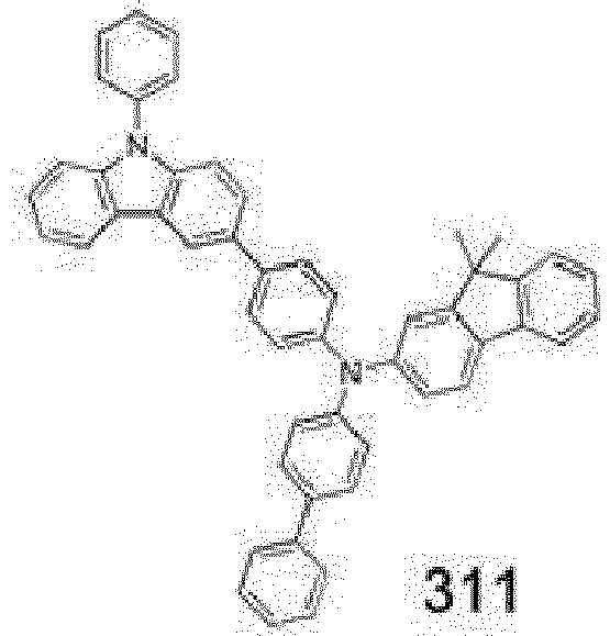
- the intermediate layer 13b may include at least one compound, for example, one selected from compounds 301, 311, and 321 shown below.
- the second electrode 13c is formed on the intermediate layer 13b.
- the second electrode 13c may be a cathode electrode, which is an electron injection electrode, and may be formed of a second electrode material having a low work function.
- the second electrode material may be one selected from a metal, an alloy, an electroconductive compound, and a mixture of these materials.
- the second electrode 13c may be formed as a reflective electrode, a semi-transparent electrode, or a transmissive electrode by forming a thin film by using a material selected from, for example, Li, Mg, Al, Al-Li, Ca, Mg-In, and Mg-Ag.
- the second electrode 13c may be formed as a transmissive electrode by using, for example, ITO or IZO to obtain a top emission organic light-emitting display device, but the present embodiment is not limited thereto.
- the organic light-emitting unit 13 may include one pixel circuit per pixel and the pixel circuit may include at least one thin film transistor (TFT) and a capacitor.
- the TFT is connected electrically to and used for driving the first electrode 13a.
- the first electrode 13a may be patterned to form each pixel, and the second electrode 13c may be formed as a common electrode to cover all the pixels.
- the second electrode 13c may be formed to have a relatively large thickness to increase light emitting efficiency towards the substrate 11.
- the second electrode 13c may be formed to have a relatively small thickness so that the second electrode 13c functions as a semi-transparent reflective film or may be formed of a transparent conductive material besides the materials described above.
- the first electrode 13a may further include a reflective film.
- an organic film 14 is formed on the second electrode 13c.
- the organic film 14 performs as a protective layer for preventing the second electrode 13c from being damaged when a thin film encapsulating structure is formed on the organic light-emitting unit 13.
- the organic film 14 is formed of a transparent material having a high refractive index to perform a reflective index matching function.
- the organic film 14 may be formed of at least one of, for example, LiF, 8-Hydroxyquinolinolato-lithium (Liq), and tris(8-hydroxy-quinolate) aluminum (Alq 3 ).
- the organic film 14 may be formed on the substrate 11 besides on an upper surface of the organic light-emitting unit 13.
- the organic film 14 may be formed as a uniform film to seal the entire organic light-emitting unit 13.
- the organic film 14 may be formed by using a resistive heating evaporation method, a sputtering method, a vacuum evaporation method, a low temperature evaporation method, an electron beam coating method, or an ion plating method.
- a resistive heating evaporation method a source is evaporated by applying heat thereto in order to deposit the source on a body to be deposited. The heat is generated by flowing an electric current through a material with electrical resistance.
- the sputtering method is a method of forming a thin film by sputtering. The other methods are also known in the art, and thus, descriptions thereof will be omitted.
- the thin film encapsulating structure includes an elastic layer 15 and an inorganic film 17 stacked on the elastic layer 15.
- the elastic layer 15 is formed on the organic film 14.
- the elastic layer 15 is a film stress solving layer for reducing stress between the organic film 14 and the inorganic film 17 that is to be formed.
- the elastic layer 15 includes an elastomer.
- the elastomer includes an organic material and an inorganic material having elasticity.
- the elastomer may be a transparent elastomer for light emission.
- the elastic layer 15 may include at least one material selected from a first group of poly dimethyl siloxane (PDMS), polysilicon, transparent poly-urethane, and styrene block copolymer (SBC). Besides those listed above, the elastic layer 15 may include at least one material selected from a second group of PET, PI, and polyvinyl chloride (PVC). The first group includes materials having elasticity greater than the materials included in the second group. The elastic layer 15 may be formed as a single layer or a multilayer including the materials described above.
- PDMS poly dimethyl siloxane
- SBC styrene block copolymer
- the first group includes materials having elasticity greater than the materials included in the second group.
- the elastic layer 15 may be formed as a single layer or a multilayer including the materials described above.
- the elastic layer 15 may be formed on the substrate 11 besides on an upper surface of the organic film 14.
- the elastic layer 15 may be formed as a uniform film to cover the entire organic light-emitting unit 13. In this way, the elastic layer 15 may further tightly seal the organic light-emitting unit 13 and the organic film 14.
- the elastic layer 15 may be formed to contact the upper surface of the organic film 14, to contact side surfaces of the organic film 14, and to contact the substrate 11.
- the elastic layer 15 may be formed by using a resistive heating evaporation method, a sputtering method, a vacuum evaporation method, a low temperature evaporation method, an electron beam coating method, or an ion plating method.
- the inorganic film 17 is formed on the elastic layer 15.
- the inorganic film 17 may be formed to contact the upper surface of the elastic layer 15, to contact side surfaces of the elastic layer 15, and to contact the substrate 11.
- the inorganic film 17 includes a low temperature viscosity transition (LVT) inorganic material (hereinafter, an LVT inorganic material).
- LVT low temperature viscosity transition
- a pre-inorganic layer that includes an LVT inorganic material is formed on the elastic layer 15 by providing the LVT inorganic material on the elastic layer 15.
- the LVT inorganic material has a low temperature changing in viscosity.
- the temperature changing in viscosity does not denote a temperature at which the viscosity of the LVT inorganic material changes from a 'solid' to a 'liquid', but denotes a minimum temperature at which the LVT inorganic material becomes fluid.
- the temperature changing in viscosity of the LVT inorganic material may be lower than a transition temperature (e.g., a deformation temperature) of a material included in the organic light-emitting unit 13.
- a transition temperature e.g., a deformation temperature
- the deformation temperature of a material included in an organic light-emitting unit denotes a temperature at which a chemical and/or physical deformation of a material included in the organic light-emitting unit 13 is caused.
- the deformation temperature of a material included in an organic light-emitting unit may denote a glass transition temperature Tg of an organic material included in the intermediate layer 13b of the organic light-emitting unit 13.
- the glass transition temperature Tg may be identified by performing a thermal analysis with respect to a material included in the organic light-emitting unit 13 by using thermo gravimetric analysis (TGA) and differential scanning calorimetry (DSC).
- the thermal analysis may be conducted under N 2 atmosphere, and using a temperature span of about room temperature to about 600 °C (at a heating rate of 10 °C/min) for TGA, and from room temperature to 400 °C for DSC, and a Pt pan for TGA, and disposable Al pan for DSC.
- the thermal analysis process is known in the art, and thus, detailed descriptions thereof will be omitted.
- the deformation temperature of a material included in the organic light-emitting unit 13 may exceed, for example, about 130 °C, but is not limited thereto, and may be readily measured through the TGA analysis described above with respect to a material included in the organic light-emitting unit 13.
- the temperature changing in viscosity of the LVT inorganic material may be greater than about 80 °C, in one embodiment, in a range from about 80 °C to about 130 °C, but is not limited thereto.
- the temperature changing in viscosity of the LVT inorganic material may be in a range from about 80 °C to about 120 °C or in a range from about 100 °C to about 120 °C, but the temperature is not limited thereto.
- the LVT inorganic material may consist of one compound or more than two compounds of different kinds.
- the LVT inorganic material may include a tin oxide, for example, SnO or SnO 2 .
- the content of SnO may be in a range from about 20 wt% to about 100 wt%.
- the LVT inorganic material may further include one material selected from the group consisting of a phosphorus oxide, for example, P 2 O 5 , boron phosphate BPO 4 , a tin fluoride, for example, SnF 2 , a niobium oxide, for example, NbO, and a tungsten oxide, for example, WO 3 , but the materials are not limited thereto.
- the LVT inorganic material may include:
- the materials to be included in the LVT inorganic material are not limited to the above list.
- the LVT inorganic material may have a composition selected from the following group, but the composition is not limited thereto:
- the LVT inorganic material may include SnO (42.5 wt%), SnF 2 (40 wt%), P 2 O 5 (15 wt%), and WO 3 (2.5 wt%), but the materials are not limited thereto.
- the pre-inorganic layer may be formed by using a resistive heating evaporation method, a sputtering method, a vacuum evaporation method, a low temperature evaporation method, an electron beam coating method, or an ion plating method.
- the LVT inorganic material may be provided by using a plasma chemical vapor deposition (PECVD) method or a plasma ion assisted deposition (PIAD) method, but the methods are not limited thereto.
- PECVD plasma chemical vapor deposition
- PIAD plasma ion assisted deposition
- an LVT inorganic material having a composition of SnO-SnF 2 -P 2 O 5 -WO 3 may be provided on the elastic layer 15 through a sputtering method.
- the sputtering method may be a dual rotary target method or a facing target method using a DC pulse power source, and a scanning method may be used by moving the substrate 11.
- Argon plasma having a power in a range from about 4 kW to about 20 kW and a pressure in a range from about 0.3 Pa to about 1.5 Pa may be used.
- a pre-inorganic layer having a desired thickness (for example, approximately 1 ⁇ m) may be obtained by repeating the scanning several times.
- the pre-inorganic layer formed in this way may include defects, such as film forming elements or pin holes.
- the film forming elements denote agglomerated particles of the LVT inorganic material that does not contribute to the film formation when the LVT inorganic material forms a film.
- the pin holes are regions where the elastic layer 15 is exposed in places where the LVT inorganic material is not provided.
- the defects of the LVT inorganic material described above may be the paths for external materials, for example, moisture or oxygen, to enter when the organic light-emitting display device is operated or stored. Accordingly, the defects of the LOT inorganic material may be causes of dark spots developed progressively, and also, may be the cause of reduced lifetime of the organic light-emitting display device.
- a healing process for removing the defects of the pre-inorganic layer may be performed.
- the healing process may be performed at a temperature greater than a temperature changing in viscosity of the LVT inorganic material.
- the healing process may be performed by heat treating the pre-inorganic layer at a temperature in a range from the temperature changing in viscosity of the LVT inorganic material or above, to less than the deformation temperature of a material included in the organic light-emitting unit 13.
- the temperature changing in viscosity of the LVT inorganic material may vary according to the composition of the LVT inorganic material, and the deformation temperature of a material included in the organic light-emitting unit 13 may vary according to the material of the organic light-emitting unit 13.
- the temperature changing in viscosity of the LVT inorganic material may be readily recognized by one of ordinary skill in the art according to the composition of the LVT inorganic material and the deformation temperature of the material included in the organic light-emitting unit 13 can be obtained (for example, by conducting Tg evaluation from a TGA result with respect to the material included in the organic light-emitting unit 13).
- the healing process may be performed by heat treating the pre-inorganic layer at a temperature in a range from about 80 °C to about 130 °C for a time period in a range from about one hour to about three hours (for example, a temperature of 110 °C for two hours), but the healing process is not limited thereto.
- the temperature for the healing process is in the above range, fluidization of the LVT inorganic material of the pre-inorganic layer is possible and the deformation of the organic light-emitting unit 13 may be reduced or prevented.
- the healing process may be performed in an infrared (IR) oven under a vacuum atmosphere or an inert gas atmosphere (for example, under an N 2 or Ar atmosphere) to prevent the organic light-emitting unit 13 from being exposed to an external atmosphere through the pin holes of the pre-inorganic layer.
- IR infrared
- the LVT inorganic material included in the pre-inorganic layer may be fluidized.
- the fluidized LVT inorganic material may have flowability. Accordingly, in the healing process, the fluidized LVT inorganic material may flow and fill the pin holes of the pre-inorganic layer, and film forming elements may also flow and fill in the pin holes.
- a highly dense inorganic film 17 may be formed because the defects of the pre-inorganic layer are removed.
- the inorganic film 17 may have a thickness in a range from about 1 ⁇ m to about 30 ⁇ m, for example, in a range from about 1 ⁇ m to about 5 ⁇ m. In one embodiment, when the thickness of the inorganic film 17 is in the range from about 1 ⁇ m to about 5 ⁇ m, a flexible organic light-emitting display device having a bending characteristic is realized. Also, because it is possible to form the inorganic film 17 as a thin film as described above, the realization of a flexible organic light-emitting display device having a bending characteristic is possible. In this way, an organic light-emitting display device having a long lifetime and flexible characteristic may be realized.
- FIGS. 4 and 5 are schematic cross-sectional views for comparing an effect of an organic light-emitting display device.
- FIGS. 4 and 5 a structure in which the inorganic film 17 is directly formed on the organic film 14, which is directly formed on the organic light-emitting unit 13, is shown. That is, FIGS. 4 and 5 show a structure in which a thin film encapsulation by using only the inorganic film 17 on the organic light-emitting unit 13 on which the organic film 14 is formed.
- FIGS. 4 and 5 show a structure in which a thin film encapsulation by using only the inorganic film 17 on the organic light-emitting unit 13 on which the organic film 14 is formed.
- an adhesive force between the inorganic film 17 and the organic film 14 is weak due to a material difference.
- the inorganic film 17 and the organic film 14 have different thermal expansion coefficients.
- interfacial delamination may occur at an interface between the inorganic film 17 and the organic film 14 or a defect such as cracks may occur in the inorganic film 17 that has a dense film quality.
- the organic light-emitting display device may be degraded by moisture or oxygen penetrated into the organic light-emitting unit 13. Therefore, a light emission characteristic of the organic light-emitting display device may be reduced and dark spots and pixel shrinkage may occur in the organic light-emitting display device.
- the above problems may be solved by including the elastic layer 15 between the organic film 14 and the inorganic film 17. Because the elastic layer 15 is formed of an elastic material, stress, which is the main cause of defects of the inorganic film 17, between the organic film 14 and the inorganic film 17 may be reduced.
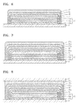
- FIG. 6 is a schematic cross-sectional view illustrating an organic light-emitting display device according to another embodiment.
- An aspect of the organic light-emitting display device depicted in FIG. 6 is that an adhesion promoting layer 16 is further formed between the elastic layer 15 and the inorganic film 17 when compared to the organic light-emitting display device depicted in FIG. 3 .
- Constituent elements in the organic light-emitting display device of FIG. 6 perform substantially the same functions as or similar functions to the corresponding constituent elements in the organic light-emitting display device of FIG. 3 , and thus, the descriptions thereof will be omitted.
- the adhesion promoting layer 16 promotes adhesion between the elastic layer 15 and the inorganic film 17.
- the elastic layer 15 includes an organic material
- the elastic layer 15 forms an organic-inorganic interface with the inorganic film 17. Therefore, although the organic material has elasticity, the adhesion force between the elastic layer 15 and the inorganic film 17 may be weaker than the adhesion force at an inorganic-inorganic interface. Accordingly, a further sound thin film encapsulating structure that increases the adhesion force between the elastic layer 15 and the inorganic film 17 may be realized by disposing the adhesion promoting layer 16 between the elastic layer 15 and the inorganic film 17.
- the adhesion promoting layer 16 may include at least one of a metal oxide and an organometallic compound.
- the adhesion promoting layer 16 may be formed as a single layer or a multilayer including the materials described above.
- the adhesion promoting layer 16 may be formed on the substrate 11 besides on an upper surface of the elastic layer 15.
- the adhesion promoting layer 16 may be formed as a uniform film to cover the entire organic light-emitting unit 13. In this way, the adhesion promoting layer 16 may further tightly seal the organic light-emitting unit 13 and the organic film 14.
- the adhesion promoting layer 16 may be formed to contact the upper surface of the elastic layer 15, to contact side surfaces of the elastic layer 15, and to contact the substrate 11, with the inorganic film 17 formed over the adhesion promoting layer 16.
- the adhesion promoting layer 16 may be formed by using a resistive heating evaporation method, a sputtering method, a vacuum evaporation method, a low temperature evaporation method, an electron beam coating method, or an ion plating method.
- FIG. 7 is a schematic cross-sectional view illustrating an organic light-emitting display device according to another embodiment.
- a second elastic layer 15b and a second inorganic film 17b are further sequentially formed on a first inorganic film 17a in comparison with the organic light-emitting display device of FIG. 6 .
- Constituent elements in the organic light-emitting display device of FIG. 7 perform substantially the same functions as or similar functions to the corresponding constituent elements in the organic light-emitting display device of FIG. 6 , and thus, the descriptions thereof will be omitted.
- a film stress is proportional to a film thickness. Accordingly, in order to reduce a film stress, the inorganic film 17 is deposited by dividing it into the first inorganic film 17a and the second inorganic film 17b. Also, in order to reduce a film stress between the first inorganic film 17a and the second inorganic film 17b, the second elastic layer 15b is formed therebetween. In this case, the elastic layer 15 formed on the organic film 14 is referred to as a first elastic layer 15a.
- the second elastic layer 15b is formed on the first inorganic film 17a which is the inorganic film 17 of FIG. 6 .
- the method of forming the second elastic layer 15b, materials that constitute the second elastic layer 15b, and the type of the second elastic layer 15b are substantially the same as in the case of the elastic layer 15 described with reference to FIGS. 1 through 3 , and thus, the descriptions thereof will not be repeated.
- the second inorganic film 17b is formed on the second elastic layer 15b.
- the method of forming the second inorganic film 17b, materials that constitute the second inorganic film 17b, and the type of the second inorganic film 17b are substantially the same as in the case of the inorganic film 17 described with reference to FIGS. 1 through 3 , and thus, the descriptions thereof will not be repeated.
- the first and second inorganic films 17a and 17b have a thickness smaller than that of the inorganic film 17 described in FIGS. 3 and 6 .
- the inorganic film 17 of FIGS. 3 and 6 may have a thickness in a range from about 1 ⁇ m to about 30 ⁇ m, for example, in a range from about 1 ⁇ m to about 5 ⁇ m.
- the first inorganic film 17a of FIG. 7 may have a thickness of about 1 ⁇ m or less
- the second inorganic film 17b may have a thickness of about 1 ⁇ m or less. That is, in the previous embodiment, the inorganic film 17 is formed to have a thickness in a range from about 1 ⁇ m to about 5 ⁇ m.
- a plurality of inorganic films each having a thickness of about 1 ⁇ m or less is formed. In this way, a film stress may be reduced and the sealing quality of the thin film encapsulating structure may be improved.
- the inorganic films are formed twice.
- the inorganic films may be formed more than three times, and also, in this case, elastic layers may be formed between the inorganic films in order to reduce stress between the inorganic films.
- an elastic layer is formed between the inorganic films.
- an adhesion promoting layer may further be formed between the elastic layer and the inorganic film.
- FIG. 8 is a schematic cross-sectional view illustrating an organic light-emitting display device according to yet another embodiment of the present embodiment.
- an encapsulation substrate 21 is further formed on an outermost inorganic film 17b when compared to the organic light-emitting display device of FIG. 7 .
- Constituent elements in the organic light-emitting display device of FIG. 8 perform substantially the same functions as or similar functions to the corresponding constituent elements in the organic light-emitting display device of FIG. 7 , and thus, the descriptions thereof will be omitted.
- the encapsulation substrate 21 is disposed on an outermost side of the thin film encapsulating structure to further reinforcing the sealing structure, and thus, protecting the organic light-emitting display device from an external impact.
- the encapsulation substrate 21 may be formed of the same material as the substrate 11.
- the encapsulation substrate 21 may be formed as a transparent substrate to transmit light.
- the encapsulation substrate 21 is disposed on an outermost inorganic film.
- the encapsulation substrate 21 is disposed on the second inorganic film 17b of the thin film encapsulating structure of FIG. 7 , as an example.
- the embodiments of the present embodiment include a structure in which an encapsulation substrate is formed on an upper side of the inorganic film in the thin film encapsulating structure of FIG. 3 ; a structure in which an encapsulation substrate is formed on an upper side of the inorganic film in the thin film encapsulating structure of FIG. 6 ; and a structure in which an encapsulation substrate is formed on an upper side of the second inorganic film in the thin film encapsulating structure of FIG. 7 and an adhesion promoting layer is further formed between the second elastic layer and the second inorganic film.
- the encapsulation substrate may further be formed on an outermost inorganic film of a thin film encapsulating structure formed by combining the embodiments.
Landscapes
- Engineering & Computer Science (AREA)
- Manufacturing & Machinery (AREA)
- Chemical & Material Sciences (AREA)
- Inorganic Chemistry (AREA)
- Physics & Mathematics (AREA)
- Optics & Photonics (AREA)
- Microelectronics & Electronic Packaging (AREA)
- Electroluminescent Light Sources (AREA)
Abstract
Description
- The following description relates to an organic light-emitting display device and a method of manufacturing the same.
- Organic light-emitting display devices are emissive display devices and have characteristics of a large viewing angle, high contrast, rapid response time, high brightness, suitable driving voltage, and fast response speed, and may display a multicolor image.
- An organic light-emitting display device includes an organic light-emitting unit that includes a lower electrode, an organic layer, and an upper electrode. The organic light-emitting unit is very susceptible to damage from external agents, for example, oxygen or moisture, and thus, a structure that seals the organic light-emitting unit from the external agents is needed.
- Also, there is a desire to develop a thin organic light-emitting display device and/or a flexible organic light-emitting display device.
- Aspects of embodiments of the present invention are directed toward an organic light-emitting display device having a strong and thin encapsulation structure, and a method of manufacturing the same.
- According to an embodiment of the present embodiment, an organic light-emitting display device includes: a substrate; an organic light-emitting unit that is formed on the substrate and includes a first electrode, an intermediate layer, and a second electrode; an organic film formed on the organic light-emitting unit; a first elastic layer that is formed on the organic film and includes an elastomer; and a first inorganic film that is formed on the first elastic layer and includes a low temperature viscosity transition (LVT) inorganic material.
- The elastomer may be a transparent elastomer.
- The elastomer may include at least one of poly dimethyl siloxane (PDMS), polysilicon, transparent poly-urethane, and styrene block copolymer (SBC).
- The LVT inorganic material may include a tin oxide.
- The first elastic layer and the first inorganic film may be formed on the substrate.
- The organic light-emitting display device may further include an adhesion promoting layer between the first elastic layer and the first inorganic film.
- The adhesion promoting layer may include at least one of a metal oxide and an organometallic compound.
- The organic light-emitting display device may further include: a second elastic layer that is formed on the first inorganic film and includes the elastomer; and a second inorganic film that is formed on the second elastic layer and includes the LVT inorganic material.
- The organic light-emitting display device may further include an encapsulation substrate formed on the second inorganic film.
- According to an embodiment of the present invention, a method of manufacturing an organic light-emitting display device includes:: forming an organic light-emitting unit that includes a first electrode, an intermediate layer, and a second electrode on a substrate; forming an organic film on the organic light-emitting unit; forming a first elastic layer that includes an elastomer on the organic film; and forming a first inorganic film that includes an LVT inorganic material on the first elastic layer.
- The elastomer may include at least one of PDMS, polysilicon, transparent poly-urethane, and SBC.
- The forming of the first inorganic film may include: forming a first pre-inorganic layer that includes the LVT inorganic material by providing the LVT inorganic material on the first elastic layer; and healing the first pre-inorganic layer at a temperature greater than a temperature changing in viscosity of the LVT inorganic material.
- The first elastic layer and the first inorganic film may be formed on the substrate.
- The method may further include forming an adhesion promoting layer that includes at least one of a metal oxide and an organometallic compound between the first elastic layer and the first inorganic film.
- The method may further include: forming a second elastic layer that includes an elastomer on the first inorganic film; and forming a second inorganic film that includes the LVT inorganic material on the second elastic layer.
- According to an aspect of the invention, there is provided an organic light-emitting display device as set out in claim 1. Preferred features of this aspect are set out in claims 2 to 9.
- According to another aspect of the invention, there is provided method of manufacturing an organic light-emitting display device as set out in claim 10. Preferred features of this aspect are set out in
claims 11 to 15. - According to the embodiments of the present embodiment, an elastic layer is formed between an organic film and an inorganic film to reduce stress between the organic film and the inorganic film, and thus, a strong thin encapsulation structure for an organic light-emitting display device is realized.
- Also, according to the embodiments of the present invention, a thin film encapsulation structure has a good encapsulation characteristic with respect to external agents, and thus, the organic light-emitting display device including the thin film encapsulation structure may have a long lifespan.
- The above and other features and enhancements of the present embodiments will become more apparent by describing in more detail example embodiments thereof with reference to the attached drawings in which:
-
FIGS. 1 through 3 are schematic cross-sectional views sequentially illustrating a method of manufacturing an organic light-emitting display device according to an embodiment; -
FIGS. 4 and 5 are schematic cross-sectional views for comparing an effect of an organic light-emitting display device; -
FIG. 6 is a schematic cross-sectional view illustrating an organic light-emitting display device according to another embodiment; -
FIG. 7 is a schematic cross-sectional view illustrating an organic light-emitting display device according to another embodiment; and -
FIG. 8 is a schematic cross-sectional view illustrating an organic light-emitting display device according to yet another embodiment. - The configurations and operations according to embodiments will be described more fully with reference to the accompanying drawings, in which example embodiments are shown.
- In the current specification, parts that are not related to the embodiments are omitted in the drawings and are not described or just briefly shown in the drawings and briefly described. Also, in the drawings, the lengths and sizes of layers and regions may be exaggerated for clarity.
- Like reference numerals are used for elements that are substantially identical or correspond to each other throughout the description of the figures. The terms 'first', 'second', etc. in the current specification may be used to describe various elements, and these elements should not be limited by these terms but are only used to distinguish one element from another. Also, it will be understood that when a layer, a region, or an element is referred to as being "formed on" another element or layer, it may include a case when the layer, the region, or the element is directly formed on the other layer, region, or element, and it may also include a case when the layer, the region, or the element is formed on the other layer, region, or element with the presence of an intervening layer(s), region(s), or element(s). Further, the use of "may" when describing embodiments of the present invention refers to "one or more embodiments of the present invention."
-
FIGS. 1 through 3 are schematic cross-sectional views sequentially illustrating a method of manufacturing an organic light-emitting display device according to an embodiment. - First, a
substrate 11 is prepared. Thesubstrate 11 may be a substrate generally used in an organic light-emitting display device. Thesubstrate 11 may be formed of a material having characteristics such as high mechanical strength, thermal stability, surface planarity, ease of handling, and waterproofness. - The
substrate 11 may be formed of a rigid material. Thesubstrate 11 may be, for example, a glass substrate, a plastic substrate, a metal substrate, or a carbon fiber substrate. When the organic light-emitting display device is a flexible display device, thesubstrate 11 may be formed of a flexible material. In this case, thesubstrate 11 may be, for example, one of a polyimide (PI) substrate and a polyethylene terephthalate (PET) substrate. - An organic light-emitting
unit 13 is formed on thesubstrate 11. The organic light-emittingunit 13 may have a structure in which afirst electrode 13a, anintermediate layer 13b, and asecond electrode 13c are sequentially formed on thesubstrate 11. - The
first electrode 13a may be formed by providing a first electrode material on thesubstrate 11 by using a deposition method or a sputtering method. When thefirst electrode 13a is an anode electrode, a lower electrode material may be selected from materials having a high work function so that holes are readily injected onto thefirst electrode 13. According to the organic light-emitting display device, thefirst electrode 13a may be a reflective electrode, a semi-transparent electrode, or a transmissive electrode. In some embodiments, the first electrode material may be a highly transparent conductive material selected from, for example, indium tin oxide (ITO), indium zinc oxide (IZO), tin oxide ((SnO2), and zinc oxide (ZnO). When thefirst electrode 13a is formed of a material selected from Mg, Al, Al-Li, Ca, Mg-In, and Mg-Ag, thefirst electrode 13a may be formed as a reflective electrode. - The
first electrode 13a may have a single layer or a multilayer structure having more than two layers. For example, thefirst electrode 13a may have a three layer structure of ITO/Ag/ITO in order to form a top emission device, but the present embodiment is not limited thereto. - The
intermediate layer 13b is formed on thefirst electrode 13a. - The
intermediate layer 13b may include at least one layer selected from a hole injection layer, a hole transport layer, a functional layer simultaneously having a hole injection function and a hole transport function, a buffer layer, an electrode blocking layer, a light-emitting layer, a hole blocking layer, an electron transport layer, and an electron injection layer. - The
intermediate layer 13b may include at least one compound, for example, one selected from compounds 301, 311, and 321 shown below. -

-
-

- The
second electrode 13c is formed on theintermediate layer 13b. Thesecond electrode 13c may be a cathode electrode, which is an electron injection electrode, and may be formed of a second electrode material having a low work function. The second electrode material may be one selected from a metal, an alloy, an electroconductive compound, and a mixture of these materials. In some embodiments, thesecond electrode 13c may be formed as a reflective electrode, a semi-transparent electrode, or a transmissive electrode by forming a thin film by using a material selected from, for example, Li, Mg, Al, Al-Li, Ca, Mg-In, and Mg-Ag. In some embodiments, thesecond electrode 13c may be formed as a transmissive electrode by using, for example, ITO or IZO to obtain a top emission organic light-emitting display device, but the present embodiment is not limited thereto. - Although not shown in
FIG. 1 , the organic light-emittingunit 13 may include one pixel circuit per pixel and the pixel circuit may include at least one thin film transistor (TFT) and a capacitor. The TFT is connected electrically to and used for driving thefirst electrode 13a. - The
first electrode 13a may be patterned to form each pixel, and thesecond electrode 13c may be formed as a common electrode to cover all the pixels. - In the case of a bottom emission organic light-emitting display device which displays an image in a direction towards the
substrate 11, thesecond electrode 13c may be formed to have a relatively large thickness to increase light emitting efficiency towards thesubstrate 11. - In the case of a top emission organic light-emitting display device which displays an image in a direction towards the
second electrode 13c, thesecond electrode 13c may be formed to have a relatively small thickness so that thesecond electrode 13c functions as a semi-transparent reflective film or may be formed of a transparent conductive material besides the materials described above. Also, in this case, thefirst electrode 13a may further include a reflective film. - Next, an
organic film 14 is formed on thesecond electrode 13c. Theorganic film 14 performs as a protective layer for preventing thesecond electrode 13c from being damaged when a thin film encapsulating structure is formed on the organic light-emittingunit 13. Also, when the organic light-emittingunit 13 is a top emission organic light-emitting unit in which light is emitted towards thesecond electrode 13c, theorganic film 14 is formed of a transparent material having a high refractive index to perform a reflective index matching function. In some embodiments, theorganic film 14 may be formed of at least one of, for example, LiF, 8-Hydroxyquinolinolato-lithium (Liq), and tris(8-hydroxy-quinolate) aluminum (Alq3). Theorganic film 14 may be formed on thesubstrate 11 besides on an upper surface of the organic light-emittingunit 13. Theorganic film 14 may be formed as a uniform film to seal the entire organic light-emittingunit 13. - The
organic film 14 may be formed by using a resistive heating evaporation method, a sputtering method, a vacuum evaporation method, a low temperature evaporation method, an electron beam coating method, or an ion plating method. In the resistive heating evaporation method, a source is evaporated by applying heat thereto in order to deposit the source on a body to be deposited. The heat is generated by flowing an electric current through a material with electrical resistance. The sputtering method is a method of forming a thin film by sputtering. The other methods are also known in the art, and thus, descriptions thereof will be omitted. - Next, as shown in
FIGS. 2 and 3 , a thin film encapsulating structure is formed on the organic light-emittingunit 13 that is covered by theorganic film 14. The thin film encapsulating structure according to the current embodiment includes anelastic layer 15 and aninorganic film 17 stacked on theelastic layer 15. - Referring to
FIG. 2 , theelastic layer 15 is formed on theorganic film 14. Theelastic layer 15 is a film stress solving layer for reducing stress between theorganic film 14 and theinorganic film 17 that is to be formed. Theelastic layer 15 includes an elastomer. The elastomer includes an organic material and an inorganic material having elasticity. When the organic light-emitting display device is of a top emission organic light-emitting display device, the elastomer may be a transparent elastomer for light emission. - For example, the
elastic layer 15 may include at least one material selected from a first group of poly dimethyl siloxane (PDMS), polysilicon, transparent poly-urethane, and styrene block copolymer (SBC). Besides those listed above, theelastic layer 15 may include at least one material selected from a second group of PET, PI, and polyvinyl chloride (PVC). The first group includes materials having elasticity greater than the materials included in the second group. Theelastic layer 15 may be formed as a single layer or a multilayer including the materials described above. - The
elastic layer 15 may be formed on thesubstrate 11 besides on an upper surface of theorganic film 14. Theelastic layer 15 may be formed as a uniform film to cover the entire organic light-emittingunit 13. In this way, theelastic layer 15 may further tightly seal the organic light-emittingunit 13 and theorganic film 14. In other words, in some embodiments, theelastic layer 15 may be formed to contact the upper surface of theorganic film 14, to contact side surfaces of theorganic film 14, and to contact thesubstrate 11. - The
elastic layer 15 may be formed by using a resistive heating evaporation method, a sputtering method, a vacuum evaporation method, a low temperature evaporation method, an electron beam coating method, or an ion plating method. - Referring to
FIG. 3 , theinorganic film 17 is formed on theelastic layer 15. In some embodiments, theinorganic film 17 may be formed to contact the upper surface of theelastic layer 15, to contact side surfaces of theelastic layer 15, and to contact thesubstrate 11. - The
inorganic film 17 includes a low temperature viscosity transition (LVT) inorganic material (hereinafter, an LVT inorganic material). Hereinafter, a method of forming the LVT inorganic material will be described in more detail. - First, a pre-inorganic layer that includes an LVT inorganic material is formed on the
elastic layer 15 by providing the LVT inorganic material on theelastic layer 15. - The LVT inorganic material has a low temperature changing in viscosity.
- In the current specification, the temperature changing in viscosity does not denote a temperature at which the viscosity of the LVT inorganic material changes from a 'solid' to a 'liquid', but denotes a minimum temperature at which the LVT inorganic material becomes fluid.
- The temperature changing in viscosity of the LVT inorganic material may be lower than a transition temperature (e.g., a deformation temperature) of a material included in the organic light-emitting
unit 13. - The deformation temperature of a material included in an organic light-emitting unit denotes a temperature at which a chemical and/or physical deformation of a material included in the organic light-emitting
unit 13 is caused. For example, the deformation temperature of a material included in an organic light-emitting unit may denote a glass transition temperature Tg of an organic material included in theintermediate layer 13b of the organic light-emittingunit 13. The glass transition temperature Tg may be identified by performing a thermal analysis with respect to a material included in the organic light-emittingunit 13 by using thermo gravimetric analysis (TGA) and differential scanning calorimetry (DSC). The thermal analysis may be conducted under N2 atmosphere, and using a temperature span of about room temperature to about 600 °C (at a heating rate of 10 °C/min) for TGA, and from room temperature to 400 °C for DSC, and a Pt pan for TGA, and disposable Al pan for DSC. The thermal analysis process is known in the art, and thus, detailed descriptions thereof will be omitted. - The deformation temperature of a material included in the organic light-emitting
unit 13 may exceed, for example, about 130 °C, but is not limited thereto, and may be readily measured through the TGA analysis described above with respect to a material included in the organic light-emittingunit 13. - Here, the temperature changing in viscosity of the LVT inorganic material may be greater than about 80 °C, in one embodiment, in a range from about 80 °C to about 130 °C, but is not limited thereto. For example, the temperature changing in viscosity of the LVT inorganic material may be in a range from about 80 °C to about 120 °C or in a range from about 100 °C to about 120 °C, but the temperature is not limited thereto.
- The LVT inorganic material may consist of one compound or more than two compounds of different kinds.
- The LVT inorganic material may include a tin oxide, for example, SnO or SnO2.
- When the LVT inorganic material includes SnO, the content of SnO may be in a range from about 20 wt% to about 100 wt%.
- For example, the LVT inorganic material may further include one material selected from the group consisting of a phosphorus oxide, for example, P2O5, boron phosphate BPO4, a tin fluoride, for example, SnF2, a niobium oxide, for example, NbO, and a tungsten oxide, for example, WO3, but the materials are not limited thereto. For example, the LVT inorganic material may include:
- SnO;
- SnO and P2O5;
- SnO and BPO4;
- SnO, SnF2, and P2O5;
- SnO, SnF2, P2O5, and NbO; or
- SnO, SnF2, P2O5, and WO3;
- The materials to be included in the LVT inorganic material are not limited to the above list.
- For example, the LVT inorganic material may have a composition selected from the following group, but the composition is not limited thereto:
- SnO (100 wt%);
- SnO (80 wt%) and P2O5 (20 wt%);
- SnO (90 wt%) and BPO4 (10 wt%);
- SnO (20-50 wt%), SnF2 (30-60 wt%), and P2O5 (10-30 wt%) (where, a sum of weights of SnO, SnF2 and P2O5 is 100 wt%);
- SnO (20-50 wt%), SnF2 (30-60 wt%), P2O5 (10-30 wt%), and NbO (1-5 wt%) (where, a sum of weight of SnO, SnF2, P2O5, and NbO is 100 wt%); and
- SnO (20-50 wt%), SnF2 (30-60 wt%), P2O5 (10-30 wt%), and WO3 (1-5 wt%) (where, a sum of weight of SnO, SnF2, P2O5, and WO3 is 100 wt%).
- For example, the LVT inorganic material may include SnO (42.5 wt%), SnF2 (40 wt%), P2O5 (15 wt%), and WO3 (2.5 wt%), but the materials are not limited thereto.
- The pre-inorganic layer may be formed by using a resistive heating evaporation method, a sputtering method, a vacuum evaporation method, a low temperature evaporation method, an electron beam coating method, or an ion plating method.
- For example, the LVT inorganic material may be provided by using a plasma chemical vapor deposition (PECVD) method or a plasma ion assisted deposition (PIAD) method, but the methods are not limited thereto.
- According to the current embodiment, an LVT inorganic material having a composition of SnO-SnF2-P2O5-WO3 may be provided on the
elastic layer 15 through a sputtering method. The sputtering method may be a dual rotary target method or a facing target method using a DC pulse power source, and a scanning method may be used by moving thesubstrate 11. Argon plasma having a power in a range from about 4 kW to about 20 kW and a pressure in a range from about 0.3 Pa to about 1.5 Pa may be used. A pre-inorganic layer having a desired thickness (for example, approximately 1 µm) may be obtained by repeating the scanning several times. - The pre-inorganic layer formed in this way may include defects, such as film forming elements or pin holes. The film forming elements denote agglomerated particles of the LVT inorganic material that does not contribute to the film formation when the LVT inorganic material forms a film. The pin holes are regions where the
elastic layer 15 is exposed in places where the LVT inorganic material is not provided. - The defects of the LVT inorganic material described above may be the paths for external materials, for example, moisture or oxygen, to enter when the organic light-emitting display device is operated or stored. Accordingly, the defects of the LOT inorganic material may be causes of dark spots developed progressively, and also, may be the cause of reduced lifetime of the organic light-emitting display device.
- Accordingly, after forming the pre-inorganic layer, a healing process for removing the defects of the pre-inorganic layer may be performed.
- The healing process may be performed at a temperature greater than a temperature changing in viscosity of the LVT inorganic material. For example, the healing process may be performed by heat treating the pre-inorganic layer at a temperature in a range from the temperature changing in viscosity of the LVT inorganic material or above, to less than the deformation temperature of a material included in the organic light-emitting
unit 13. The temperature changing in viscosity of the LVT inorganic material may vary according to the composition of the LVT inorganic material, and the deformation temperature of a material included in the organic light-emittingunit 13 may vary according to the material of the organic light-emittingunit 13. However, the temperature changing in viscosity of the LVT inorganic material may be readily recognized by one of ordinary skill in the art according to the composition of the LVT inorganic material and the deformation temperature of the material included in the organic light-emittingunit 13 can be obtained (for example, by conducting Tg evaluation from a TGA result with respect to the material included in the organic light-emitting unit 13). - For example, the healing process may be performed by heat treating the pre-inorganic layer at a temperature in a range from about 80 °C to about 130 °C for a time period in a range from about one hour to about three hours (for example, a temperature of 110 °C for two hours), but the healing process is not limited thereto. When the temperature for the healing process is in the above range, fluidization of the LVT inorganic material of the pre-inorganic layer is possible and the deformation of the organic light-emitting
unit 13 may be reduced or prevented. - The healing process may be performed in an infrared (IR) oven under a vacuum atmosphere or an inert gas atmosphere (for example, under an N2 or Ar atmosphere) to prevent the organic light-emitting
unit 13 from being exposed to an external atmosphere through the pin holes of the pre-inorganic layer. - In the healing process, the LVT inorganic material included in the pre-inorganic layer may be fluidized. The fluidized LVT inorganic material may have flowability. Accordingly, in the healing process, the fluidized LVT inorganic material may flow and fill the pin holes of the pre-inorganic layer, and film forming elements may also flow and fill in the pin holes.
- As a result, a highly dense
inorganic film 17 may be formed because the defects of the pre-inorganic layer are removed. - The
inorganic film 17 may have a thickness in a range from about 1 µm to about 30 µm, for example, in a range from about 1 µm to about 5 µm. In one embodiment, when the thickness of theinorganic film 17 is in the range from about 1 µm to about 5 µm, a flexible organic light-emitting display device having a bending characteristic is realized. Also, because it is possible to form theinorganic film 17 as a thin film as described above, the realization of a flexible organic light-emitting display device having a bending characteristic is possible. In this way, an organic light-emitting display device having a long lifetime and flexible characteristic may be realized. -
FIGS. 4 and 5 are schematic cross-sectional views for comparing an effect of an organic light-emitting display device. - In
FIGS. 4 and 5 , a structure in which theinorganic film 17 is directly formed on theorganic film 14, which is directly formed on the organic light-emittingunit 13, is shown. That is,FIGS. 4 and 5 show a structure in which a thin film encapsulation by using only theinorganic film 17 on the organic light-emittingunit 13 on which theorganic film 14 is formed. In the case of a structure in which theinorganic film 17 contacts theorganic film 14, an adhesive force between theinorganic film 17 and theorganic film 14 is weak due to a material difference. Also, theinorganic film 17 and theorganic film 14 have different thermal expansion coefficients. Accordingly, due to stress generated when theinorganic film 17 and theorganic film 14 expand with different degrees from each other due to heat generated from the organic light-emittingunit 13 and a surrounding temperature change, as depicted inFIG. 4 , interfacial delamination may occur at an interface between theinorganic film 17 and theorganic film 14 or a defect such as cracks may occur in theinorganic film 17 that has a dense film quality. As a result, as depicted inFIG. 5 , the organic light-emitting display device may be degraded by moisture or oxygen penetrated into the organic light-emittingunit 13. Therefore, a light emission characteristic of the organic light-emitting display device may be reduced and dark spots and pixel shrinkage may occur in the organic light-emitting display device. - However, according to the embodiments of the invention, for example as depicted in
FIG. 3 , the above problems may be solved by including theelastic layer 15 between theorganic film 14 and theinorganic film 17. Because theelastic layer 15 is formed of an elastic material, stress, which is the main cause of defects of theinorganic film 17, between theorganic film 14 and theinorganic film 17 may be reduced. -
FIG. 6 is a schematic cross-sectional view illustrating an organic light-emitting display device according to another embodiment. - An aspect of the organic light-emitting display device depicted in
FIG. 6 is that anadhesion promoting layer 16 is further formed between theelastic layer 15 and theinorganic film 17 when compared to the organic light-emitting display device depicted inFIG. 3 . Constituent elements in the organic light-emitting display device ofFIG. 6 perform substantially the same functions as or similar functions to the corresponding constituent elements in the organic light-emitting display device ofFIG. 3 , and thus, the descriptions thereof will be omitted. - The
adhesion promoting layer 16 promotes adhesion between theelastic layer 15 and theinorganic film 17. For example, when theelastic layer 15 includes an organic material, theelastic layer 15 forms an organic-inorganic interface with theinorganic film 17. Therefore, although the organic material has elasticity, the adhesion force between theelastic layer 15 and theinorganic film 17 may be weaker than the adhesion force at an inorganic-inorganic interface. Accordingly, a further sound thin film encapsulating structure that increases the adhesion force between theelastic layer 15 and theinorganic film 17 may be realized by disposing theadhesion promoting layer 16 between theelastic layer 15 and theinorganic film 17. Theadhesion promoting layer 16 may include at least one of a metal oxide and an organometallic compound. Theadhesion promoting layer 16 may be formed as a single layer or a multilayer including the materials described above. - The
adhesion promoting layer 16 may be formed on thesubstrate 11 besides on an upper surface of theelastic layer 15. Theadhesion promoting layer 16 may be formed as a uniform film to cover the entire organic light-emittingunit 13. In this way, theadhesion promoting layer 16 may further tightly seal the organic light-emittingunit 13 and theorganic film 14. In other words, in some embodiments, theadhesion promoting layer 16 may be formed to contact the upper surface of theelastic layer 15, to contact side surfaces of theelastic layer 15, and to contact thesubstrate 11, with theinorganic film 17 formed over theadhesion promoting layer 16. - The
adhesion promoting layer 16 may be formed by using a resistive heating evaporation method, a sputtering method, a vacuum evaporation method, a low temperature evaporation method, an electron beam coating method, or an ion plating method. -
FIG. 7 is a schematic cross-sectional view illustrating an organic light-emitting display device according to another embodiment. - In the organic light-emitting display device of
FIG. 7 , a secondelastic layer 15b and a secondinorganic film 17b are further sequentially formed on a firstinorganic film 17a in comparison with the organic light-emitting display device ofFIG. 6 . Constituent elements in the organic light-emitting display device ofFIG. 7 perform substantially the same functions as or similar functions to the corresponding constituent elements in the organic light-emitting display device ofFIG. 6 , and thus, the descriptions thereof will be omitted. - Generally, a film stress is proportional to a film thickness. Accordingly, in order to reduce a film stress, the
inorganic film 17 is deposited by dividing it into the firstinorganic film 17a and the secondinorganic film 17b. Also, in order to reduce a film stress between the firstinorganic film 17a and the secondinorganic film 17b, the secondelastic layer 15b is formed therebetween. In this case, theelastic layer 15 formed on theorganic film 14 is referred to as a firstelastic layer 15a. - More specifically, the second
elastic layer 15b is formed on the firstinorganic film 17a which is theinorganic film 17 ofFIG. 6 . The method of forming the secondelastic layer 15b, materials that constitute the secondelastic layer 15b, and the type of the secondelastic layer 15b are substantially the same as in the case of theelastic layer 15 described with reference toFIGS. 1 through 3 , and thus, the descriptions thereof will not be repeated. - Next, the second
inorganic film 17b is formed on the secondelastic layer 15b. The method of forming the secondinorganic film 17b, materials that constitute the secondinorganic film 17b, and the type of the secondinorganic film 17b are substantially the same as in the case of theinorganic film 17 described with reference toFIGS. 1 through 3 , and thus, the descriptions thereof will not be repeated. - According to an aspect of the present embodiment, the first and second
inorganic films inorganic film 17 described inFIGS. 3 and6 . Theinorganic film 17 ofFIGS. 3 and6 may have a thickness in a range from about 1 µm to about 30 µm, for example, in a range from about 1 µm to about 5 µm. However, the firstinorganic film 17a ofFIG. 7 may have a thickness of about 1 µm or less, and also, the secondinorganic film 17b may have a thickness of about 1 µm or less. That is, in the previous embodiment, theinorganic film 17 is formed to have a thickness in a range from about 1 µm to about 5 µm. However, in the current embodiment, a plurality of inorganic films each having a thickness of about 1 µm or less is formed. In this way, a film stress may be reduced and the sealing quality of the thin film encapsulating structure may be improved. - In
FIG. 7 , it is depicted that the inorganic films are formed twice. However, this is just an example, and the inorganic films may be formed more than three times, and also, in this case, elastic layers may be formed between the inorganic films in order to reduce stress between the inorganic films. - Also, in
FIG. 7 , an elastic layer is formed between the inorganic films. However, it is an example, that is, as depicted inFIG. 6 , an adhesion promoting layer may further be formed between the elastic layer and the inorganic film. -
FIG. 8 is a schematic cross-sectional view illustrating an organic light-emitting display device according to yet another embodiment of the present embodiment. - In the organic light-emitting display device of
FIG. 8 , anencapsulation substrate 21 is further formed on an outermostinorganic film 17b when compared to the organic light-emitting display device ofFIG. 7 . Constituent elements in the organic light-emitting display device ofFIG. 8 perform substantially the same functions as or similar functions to the corresponding constituent elements in the organic light-emitting display device ofFIG. 7 , and thus, the descriptions thereof will be omitted. - The
encapsulation substrate 21 is disposed on an outermost side of the thin film encapsulating structure to further reinforcing the sealing structure, and thus, protecting the organic light-emitting display device from an external impact. Theencapsulation substrate 21 may be formed of the same material as thesubstrate 11. When the organic light-emitting display device is a top emission organic light-emitting display device in which light is emitted towards thesecond electrode 13c, theencapsulation substrate 21 may be formed as a transparent substrate to transmit light. - In an aspect of the present embodiment, the
encapsulation substrate 21 is disposed on an outermost inorganic film. InFIG. 8 , theencapsulation substrate 21 is disposed on the secondinorganic film 17b of the thin film encapsulating structure ofFIG. 7 , as an example. - The embodiments of the present embodiment include a structure in which an encapsulation substrate is formed on an upper side of the inorganic film in the thin film encapsulating structure of
FIG. 3 ; a structure in which an encapsulation substrate is formed on an upper side of the inorganic film in the thin film encapsulating structure ofFIG. 6 ; and a structure in which an encapsulation substrate is formed on an upper side of the second inorganic film in the thin film encapsulating structure ofFIG. 7 and an adhesion promoting layer is further formed between the second elastic layer and the second inorganic film. Also, the encapsulation substrate may further be formed on an outermost inorganic film of a thin film encapsulating structure formed by combining the embodiments. - While aspects of the present invention have been particularly shown and described with reference to some example embodiments thereof, it will be understood by those of ordinary skill in the art that various changes in form and details may be made therein without departing from the scope of the present embodiment as defined by the following claims, and equivalents thereof.
Claims (15)
- An organic light-emitting display device comprising:a substrate;an organic light-emitting unit over the substrate, the organic light-emitting unit comprising a first electrode, an intermediate layer, and a second electrode;an organic film over the organic light-emitting unit;a first elastic layer comprising an elastomer over the organic film ; anda first inorganic film comprising a low temperature viscosity transition, LVT, inorganic material over the first elastic layer.
- The organic light-emitting display device of claim 1, wherein the elastomer is a transparent elastomer.
- The organic light-emitting display device of claim 1 or 2, wherein the elastomer comprises at least one selected from the group consisting of poly dimethyl siloxane (PDMS), polysilicon, transparent poly-urethane, and styrene block copolymer (SBC).
- The organic light-emitting display device of any one of claims 1 to 3, wherein the LVT inorganic material comprises a tin oxide.
- The organic light-emitting display device of any one of claims 1 to 4, wherein the first elastic layer and the first inorganic film are formed to contact the substrate.
- The organic light-emitting display device of any one of claims 1 to 5, further comprising an adhesion promoting layer arranged between the first elastic layer and the first inorganic film.
- The organic light-emitting display device of claim 6, wherein the adhesion promoting layer comprises at least one selected from the group consisting of a metal oxide and an organometallic compound.
- The organic light-emitting display device of any one of claims 1 to 7, further comprising:a second elastic layer comprising an elastomer over the first inorganic film; anda second inorganic film comprising a LVT inorganic material on the second elastic layer; optionally wherein the first elastic layer comprises the same elastomer as the second elastic layer, and the first inorganic film comprises the same LVT inorganic material as the second inorganic film.
- The organic light-emitting display device of claim 8, further comprising an encapsulation substrate over the second inorganic film.
- A method of manufacturing an organic light-emitting display device, the method comprising:forming an organic light-emitting unit over a substrate, the organic light-emitting unit comprising a first electrode, an intermediate layer, and a second electrode;forming an organic film over the organic light-emitting unit;forming a first elastic layer comprising an elastomer over the organic film; andforming a first inorganic film comprising an LVT inorganic material over the first elastic layer.
- The method of claim 10, wherein the elastomer comprises at least one selected from the group consisting of PDMS, polysilicon, transparent poly-urethane, and SBC.
- The method of claim 10 or 11, wherein the forming of the first inorganic film comprises:forming a first pre-inorganic layer comprising the LVT inorganic material by providing the LVT inorganic material on the first elastic layer; andhealing the first pre-inorganic layer at a temperature greater than a temperature changing in viscosity of the LVT inorganic material.
- The method of any one of claims 10 to 12, wherein the first elastic layer and the first inorganic film are formed on the substrate.
- The method of any one of claims 10 to 13, further comprising forming an adhesion promoting layer between the first elastic layer and the first inorganic film, the adhesion promoting layer comprising at least one selected from the group consisting of a metal oxide and an organometallic compound.
- The method of any one of claims 10 to 14, further comprising:forming a second elastic layer comprising an elastomer on the first inorganic film; andforming a second inorganic film comprising an LVT inorganic material on the second elastic layer; optionally wherein the first elastic layer comprises the same elastomer as the second elastic layer, and the first inorganic film comprises the same LVT inorganic material as the second inorganic film.
Applications Claiming Priority (1)
| Application Number | Priority Date | Filing Date | Title |
|---|---|---|---|
| KR1020130046928A KR101444065B1 (en) | 2013-04-26 | 2013-04-26 | Organic light emitting display device and method of manufacturing the same |
Publications (2)
| Publication Number | Publication Date |
|---|---|
| EP2797135A2 true EP2797135A2 (en) | 2014-10-29 |
| EP2797135A3 EP2797135A3 (en) | 2015-02-25 |
Family
ID=50112856
Family Applications (1)
| Application Number | Title | Priority Date | Filing Date |
|---|---|---|---|
| EP14155647.2A Withdrawn EP2797135A3 (en) | 2013-04-26 | 2014-02-18 | Organic Light-Emitting Display Device and Method of Manufacturing the Same |
Country Status (3)
| Country | Link |
|---|---|
| US (1) | US9232572B2 (en) |
| EP (1) | EP2797135A3 (en) |
| KR (1) | KR101444065B1 (en) |
Families Citing this family (3)
| Publication number | Priority date | Publication date | Assignee | Title |
|---|---|---|---|---|
| KR102085319B1 (en) * | 2013-07-30 | 2020-03-06 | 삼성디스플레이 주식회사 | Organic light emitting display device and method of manufacturing the same |
| WO2016199739A1 (en) * | 2015-06-12 | 2016-12-15 | シャープ株式会社 | El display device and method for manufacturing el display device |
| CN109686769B (en) * | 2018-12-25 | 2020-09-08 | 深圳市华星光电技术有限公司 | Stretchable display device and manufacturing method thereof |
Family Cites Families (10)
| Publication number | Priority date | Publication date | Assignee | Title |
|---|---|---|---|---|
| KR100413450B1 (en) | 2001-07-20 | 2003-12-31 | 엘지전자 주식회사 | protecting film structure for display device |
| JP2005190703A (en) * | 2003-12-24 | 2005-07-14 | Tohoku Pioneer Corp | Organic EL panel and manufacturing method thereof |
| JP2005298703A (en) * | 2004-04-13 | 2005-10-27 | Mitsui Chemicals Inc | Adhesive film, casing and organic EL light emitting device using the same |
| KR100635581B1 (en) | 2004-11-29 | 2006-10-17 | 삼성에스디아이 주식회사 | Organic electroluminescent display and manufacturing method thereof |
| US7722929B2 (en) | 2005-08-18 | 2010-05-25 | Corning Incorporated | Sealing technique for decreasing the time it takes to hermetically seal a device and the resulting hermetically sealed device |
| US20070040501A1 (en) | 2005-08-18 | 2007-02-22 | Aitken Bruce G | Method for inhibiting oxygen and moisture degradation of a device and the resulting device |
| US20080048178A1 (en) * | 2006-08-24 | 2008-02-28 | Bruce Gardiner Aitken | Tin phosphate barrier film, method, and apparatus |
| US20080290798A1 (en) | 2007-05-22 | 2008-11-27 | Mark Alejandro Quesada | LLT barrier layer for top emission display device, method and apparatus |
| KR20100035320A (en) * | 2008-09-26 | 2010-04-05 | 주식회사 코오롱 | Organic electroluminescent device and fabricating method of the same |
| EP2904652B1 (en) * | 2012-10-01 | 2020-07-15 | Corning Incorporated | Oled comprising light extraction substructures and display devices incorporating the same |
-
2013
- 2013-04-26 KR KR1020130046928A patent/KR101444065B1/en active Active
- 2013-08-28 US US14/012,975 patent/US9232572B2/en active Active
-
2014
- 2014-02-18 EP EP14155647.2A patent/EP2797135A3/en not_active Withdrawn
Non-Patent Citations (1)
| Title |
|---|
| None |
Also Published As
| Publication number | Publication date |
|---|---|
| US20140319997A1 (en) | 2014-10-30 |
| US9232572B2 (en) | 2016-01-05 |
| EP2797135A3 (en) | 2015-02-25 |
| KR101444065B1 (en) | 2014-09-26 |
Similar Documents
| Publication | Publication Date | Title |
|---|---|---|
| US9337445B2 (en) | Organic light-emitting display apparatus and method of manufacturing the same | |
| US9159950B2 (en) | Organic light emitting display device and method for manufacturing the same | |
| TWI625880B (en) | Organic light emitting display device | |
| KR101931177B1 (en) | Organic light emitting display device | |
| TWI679791B (en) | Light emitting element, display device and lighting device | |
| US9196863B2 (en) | Organic light emitting display device and method of manufacturing the same | |
| EP2637231A1 (en) | Method of preparing organic light-emitting device | |
| US9054057B2 (en) | Organic light-emitting display device and method of preparing the same | |
| US9614181B2 (en) | Organic light emitting display apparatus and method of manufacturing the same | |
| US20170213996A1 (en) | Organic electroluminescent element | |
| US9232572B2 (en) | Organic light-emitting display device and method of manufacturing the same | |
| US9349989B2 (en) | Organic luminescence emitting display device and method of manufacturing the same | |
| KR101114351B1 (en) | Encapsulation Structure of Organic Light Emitting Diode | |
| US20080264680A1 (en) | Voltage-Operated Layer Arrangement |
Legal Events
| Date | Code | Title | Description |
|---|---|---|---|
| PUAI | Public reference made under article 153(3) epc to a published international application that has entered the european phase |
Free format text: ORIGINAL CODE: 0009012 |
|
| 17P | Request for examination filed |
Effective date: 20140218 |
|
| AK | Designated contracting states |
Kind code of ref document: A2 Designated state(s): AL AT BE BG CH CY CZ DE DK EE ES FI FR GB GR HR HU IE IS IT LI LT LU LV MC MK MT NL NO PL PT RO RS SE SI SK SM TR |
|
| AX | Request for extension of the european patent |
Extension state: BA ME |
|
| PUAL | Search report despatched |
Free format text: ORIGINAL CODE: 0009013 |
|
| AK | Designated contracting states |
Kind code of ref document: A3 Designated state(s): AL AT BE BG CH CY CZ DE DK EE ES FI FR GB GR HR HU IE IS IT LI LT LU LV MC MK MT NL NO PL PT RO RS SE SI SK SM TR |
|
| AX | Request for extension of the european patent |
Extension state: BA ME |
|
| RIC1 | Information provided on ipc code assigned before grant |
Ipc: H01L 51/52 20060101AFI20150116BHEP |
|
| R17P | Request for examination filed (corrected) |
Effective date: 20150825 |
|
| RAP1 | Party data changed (applicant data changed or rights of an application transferred) |
Owner name: SAMSUNG DISPLAY CO., LTD. |
|
| RBV | Designated contracting states (corrected) |
Designated state(s): AL AT BE BG CH CY CZ DE DK EE ES FI FR GB GR HR HU IE IS IT LI LT LU LV MC MK MT NL NO PL PT RO RS SE SI SK SM TR |
|
| STAA | Information on the status of an ep patent application or granted ep patent |
Free format text: STATUS: EXAMINATION IS IN PROGRESS |
|
| 17Q | First examination report despatched |
Effective date: 20190723 |
|
| STAA | Information on the status of an ep patent application or granted ep patent |
Free format text: STATUS: THE APPLICATION IS DEEMED TO BE WITHDRAWN |
|
| 18D | Application deemed to be withdrawn |
Effective date: 20191203 |