EP2797100A1 - Method of using a phase plate in a transmission electron microscope - Google Patents
Method of using a phase plate in a transmission electron microscope Download PDFInfo
- Publication number
- EP2797100A1 EP2797100A1 EP13165356.0A EP13165356A EP2797100A1 EP 2797100 A1 EP2797100 A1 EP 2797100A1 EP 13165356 A EP13165356 A EP 13165356A EP 2797100 A1 EP2797100 A1 EP 2797100A1
- Authority
- EP
- European Patent Office
- Prior art keywords
- phase plate
- phase
- thin film
- sample
- electron microscope
- Prior art date
- Legal status (The legal status is an assumption and is not a legal conclusion. Google has not performed a legal analysis and makes no representation as to the accuracy of the status listed.)
- Withdrawn
Links
Images

Classifications
-
- H—ELECTRICITY
- H01—ELECTRIC ELEMENTS
- H01J—ELECTRIC DISCHARGE TUBES OR DISCHARGE LAMPS
- H01J37/00—Discharge tubes with provision for introducing objects or material to be exposed to the discharge, e.g. for the purpose of examination or processing thereof
- H01J37/26—Electron or ion microscopes; Electron or ion diffraction tubes
- H01J37/261—Details
- H01J37/263—Contrast, resolution or power of penetration
-
- H—ELECTRICITY
- H01—ELECTRIC ELEMENTS
- H01J—ELECTRIC DISCHARGE TUBES OR DISCHARGE LAMPS
- H01J2237/00—Discharge tubes exposing object to beam, e.g. for analysis treatment, etching, imaging
- H01J2237/26—Electron or ion microscopes
- H01J2237/2614—Holography or phase contrast, phase related imaging in general, e.g. phase plates
Definitions
- the invention relates to a method of using a phase plate in a transmission electron microscope, the phase plate comprising a thin film, the method comprising:
- TEM Transmission Electron Microscope
- CTF Contrast Transfer Function
- phase plate the phase plate introducing a phase difference between the diffracted beams and the undiffracted beam.
- phase plates There are two main types of phase plates: the so-called Zernike phase plate leaves the undiffracted beam unchanged, and causes a phase shift of the diffracted beams, while the so-called Boersch phase plate shifts the undiffracted beam while leaving the diffracted beams unchanged.
- phase plate changes the sine-like behavior of the CTF to a cosine-like behavior, and thus a maximum contrast for low spatial frequencies.
- phase plates and other contrast enhancing devices see " Phase Contrast Enhancement with Phase Plates in Biological Electron Microscopy", K. Nagayama et al., Microscopy Today, Vol. 18 No. 4 (July 2010), pp. 10-13 , further referred to as Nagayama [-2-].
- Boersch phase plates and Zernike phase plates require microscopic holes (typically less than 1 ⁇ m) and a centering accuracy which is even an order of magnitude better than the hole size.
- phase plate is the phase plate, as first described by Johnson [-1-].
- the phase plate described by Johnson is formed by a contamination spot on a continuous carbon film. This spot is formed using the electron beam in high current mode. The contamination spot modifies the thickness of the film, resulting in a thicker part.
- This film can then, at lower current, be used as a phase plate, where the undiffracted electrons, passing through the thick spot, experience a larger (negative) phase shift than the diffracted electrons passing through the non-contaminated (or less-contaminated) film.
- the effect of such a phase plate thus resembles the effect of Zernike phase plate, but with the difference that this phase plate gives a negative phase contrast.
- phase plate An advantage of such a phase plate is that it is self-building and thus centered.
- phase plate A disadvantage of this phase plate is that the build-up of contaminants is difficult to control, thus hampering practical use of the device
- phase plate is known from US patent application No. US 2011/0174971A1 , describing a film exposed to an electron beam, resulting in positive charging (due to secondary electron emission) and/or contamination (or the charging of contamination).
- the invention intends to provide a solution.
- preparing the phase plate involves locally building up a vacuum potential resulting from a change in the electronic structure of the thin film by irradiating the phase plate with a focused beam of electrons, the vacuum potential leading to a phase shift that is less than at the non-irradiated thin film.
- Each material has a chemical potential ⁇ that depends not only on the materials composition, but also on its phase, crystallographic properties, etc.
- the electrochemical potential ⁇ is necessarily equalized, and any difference in chemical potential thus results in a different Galvani potential.
- irradiation of a material with a beam of electrons results in bond-breaking, creating electron trapping centra that may act as p-type dopants. This may result in a material with a lower chemical potential, where electrons flow toward the p-doped area and create a negative potential.
- the irradiation with the beam locally modifies the material, possibly by bond-breaking and/or the corresponding formation of p-type dopant positions.
- phase shift is not a linear function of the deposited dose, but increases up to some maximum value that corresponds with a steady state that establishes itself.
- Inventors also found that the effect returned to its normal state, and a phase plate according to the invention using a thin film of amorphous carbon must be prepared anew with the electron beam after approximately one day.
- the phase plate is operated in a heated condition, thereby avoiding contamination.
- the heating can be achieved by e.g. laser heating of the thin film, or by heating of a part of a holder holding the thin film (typically an aperture mechanism), for example by ohmic heating.
- the thin film may further show markers, for example to help aligning the transmission electron microscope, for example to accurately setting up of beam shift pivot points and finding the in-plane condition.
- the thin film is a carbon film, more specifically an amorphous thin film, although also the use of SiN, SiB, SiC and Si films is known.
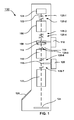
- Figure 1 schematically shows a TEM 100 equipped with a phase plate.
- Figure 1 shows a particle source 104 producing a beam of particles, such as electrons, along optical axis 102.
- the particles have a selectable energy of typically between 80 - 300 keV, although higher energies, e.g. 400 keV - 1 MeV, or lower energies, e.g. 50 keV, may be used.
- the beam of particles is manipulated by condenser system 106 to form a parallel beam impinging on a sample 108, the sample positioned with a sample holder 110.
- the sample holder can position the sample with respect to the optical axis and may shift the sample in the plane perpendicular to the optical axis and tilt the sample with respect to said axis.
- Objective lens 112 forms a magnified image of the sample.
- the objective lens is followed by a magnifying system 116, e.g. a doublet of lenses, forming an enlarged image of the back-focal plane 114 of the objective lens.
- a phase plate 118 is placed in the enlarged image of the back-focal plane of the objective lens, this conjugated plane positioned between the magnifying system and a projection system 122.
- the phase plate is positioned with a manipulator 120, allowing the phase plate to be centered round the optical axis.
- the projection system forms a magnified image of the sample on a detector 124, thereby revealing sample details of e.g. 0.1 nm.
- the detector may take the form of a fluorescent screen, or e.g. a CCD or CMOS camera.
- the screen can be viewed via the glass window 126.
- the TEM comprises a large number of deflectors, schematically shown as 128-1..128-7, although other deflectors on other places may be included.
- phase plate may also be positioned in the back-focal plane itself, in which case the magnifying system 116 is superfluous.
- the phase plate is normally formed as a thin film surrounded by a holder structure, for example a platinum aperture as commonly used in electron microscopy. Forming the phase plate with such an aperture has as an advantage that a standard aperture holder can be used to hold and position the phase plate. It is noted that heated aperture holders are known, the heating used to avoid contamination.
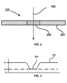
- Figure 2 schematically shows the thin film 200 that is irradiated in an area surrounding the axis 102 of the electron microscope. As a result the electronic structure of the area 202 is changed, while that of the non-irradiated area 201 is unchanged.
- Figure 3 schematically shows the potential of the thin film after irradiation. Removed from the axis the potential equals the chemical potential, but the irradiated area has an added (negative) electronic potential.
- Figure 4 schematically shows the phase shift induced as a function of irradiation time.
- phase shift is not a linear function of the dose deposited on the thin film. This implies that there is an upper limit to the Galvani potential induced by the electron beam.
- Inventors also found that when a larger area (dotted line, irradiated area with a diameter of 125 nm) was irradiated using an identical total beam current as a small area (solid line), the large area resulted in a large phase shift than the small area. This can be explained as follows: First, assume that a maximum vacuum potential can be induced. Then compare two electron beams, one passing through the irradiated part and one far removed from this part, and define z along the electron-optical axis 102.
- the integral ⁇ - ⁇ ⁇ V ( z ) dz (more accurately from the sample plane to the image plane) differs due to the vacuum potential.
- the difference between the two integrals scales with the size of the spot (assuming the same vacuum potential). Therefore the phase shift can be tuned by controlling the size of the spot that is irradiated during the preparation of the phase plate.
- the curves shown in figure 4 are obtained at identical beam current. It will be clear to the skilled person that a higher beam current, as is achievable using a larger spot size, results in a quicker settling time.
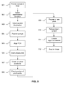
- Figure 5 schematically shows a workflow for operating a transmission electron microscope equipped with a phase plate according to the invention.
- step 501 a sample is provided in the transmission electron microscope (TEM).
- step 502 the experiments' conditions are selected, the conditions including electron beam energy, spot size condenser aperture (implying the selection of a beam current), magnification, etc.
- step 503 the condenser is set to illuminate the sample with a parallel beam of electrons.
- step 504 the sample is positioned to eucentric height (where the sample can be tilted without height variations) and focus is set (so that parallel beams in the sample plane result in focused beams in the back-focal plane of the objective lens).
- step 505 standard microscope alignments are performed.
- step 506 the phase plate is inserted in the beam path.
- the phase plate is inserted only now to minimize unwanted exposure (irradiation) of the phase plate.
- on-plane conditions (indicating whether the phase plate is exactly in the back-focal plane or slightly removed from it) are checked, for example using features on the phase plate, and the condenser lens is adjusted if necessary. As discussed earlier, by working slightly off-plane the size of the irradiated area can be tuned/selected. It is noted that the phase plate need not be in the back-focal plane, but may reside in a plane conjugated to it.
- step 508 pivot point settings of the beam are checked and image shift, using e.g. the features on the phase plate, ensuring that a tilt of the beam entering the objective lens ideally results in a pure shift in the sample plane and a pure tilt in the back-focal plane of the objective lens (and thus the plane where the phase plate resides).
- step 509 the phase plate is prepared by keeping the beam on a clean area of the phase plate for an appropriate amount of time (for example based on earlier experiments), the amount of time depending on beam intensity (beam current), beam size and phase plate material. Typically this amounts to 10 - 100 seconds of irradiation time.
- step 510 the beam current is reduced to imaging conditions as are normal for imaging samples, after which a region of interest is located on the sample.
- step 511 an image is acquired.
- the phase plate can be a heated phase plate (with a regulated temperature of, for example, between 100 °C and 400 °C) to avoid contamination. It that case step 501 should also include thermal stabilization of said temperature so that drift of the phase plate becomes negligible.
- the last steps 510 and 511 can be repeated until sufficient data is gathered from the sample. Refocusing, tilting and (mechanically) shifting the sample may be required.
Landscapes
- Chemical & Material Sciences (AREA)
- Analytical Chemistry (AREA)
- Sampling And Sample Adjustment (AREA)
- Analysing Materials By The Use Of Radiation (AREA)
Abstract
The invention relates to a method of using a phase plate (118) in a transmission electron microscope (100), the phase plate comprising a thin film, the method comprising: introducing the phase plate in the transmission electron microscope;
preparing the phase plate by irradiating the film with a focused electron beam;
introducing a sample (108) in the transmission electron microscope; and forming an image of the sample using the prepared phase plate,
characterized in that
preparing the phase plate involves locally building up a vacuum potential resulting from a change in the electronic structure of the thin film by irradiating the phase plate with a focused beam of electrons, the vacuum potential leading to an absolute phase shift |ϕ| with a smaller value than at the non-irradiated thin film.
preparing the phase plate by irradiating the film with a focused electron beam;
introducing a sample (108) in the transmission electron microscope; and forming an image of the sample using the prepared phase plate,
characterized in that
preparing the phase plate involves locally building up a vacuum potential resulting from a change in the electronic structure of the thin film by irradiating the phase plate with a focused beam of electrons, the vacuum potential leading to an absolute phase shift |ϕ| with a smaller value than at the non-irradiated thin film.
Preferably the phase plate is heated to avoid contamination. The phase shift achieved with this phase plate can be tuned by varying the diameter of the irradiated spot.
Description
- The invention relates to a method of using a phase plate in a transmission electron microscope, the phase plate comprising a thin film, the method comprising:
- introducing the phase plate in the transmission electron microscope;
- preparing the phase plate by irradiating the film with a focused electron beam;
- introducing a sample in the transmission electron microscope; and
- forming an image of a sample using the prepared phase plate.
- This method is known from "Principles and Techniques of Electron Microscopy, Vol. 3: Biological applications", Ed. M.A. Hayat, ISBN- 0-442-25674-4, Chapter 4: In-focus phase contrast electron microscopy, H.M. Johnson, Electron Optics Laboratory, Dept. of Biophysics, Roswell Park Memorial Institute, Buffalo, N.Y., USA, specifically page 174-176
- In a Transmission Electron Microscope (TEM) a sample is imaged by passing a beam of energetic electrons with a selectable energy of, for example, between 40 keV and 400 keV, through the sample. For so-called weak-phase samples, such as biological samples, most electrons pass through the sample while some electrons are elastically or inelastically scattered, the elastically scattered electrons forming diffracted beams. The image is formed by interference of the elastically scattered and unscattered electrons (diffracted and undiffracted beams).
- A problem arises in that the Contrast Transfer Function (CTF) for low spatial frequencies in the image is zero or close to zero, resulting in low visibility of large objects/structures. This is caused by the fact that a camera or fluorescent screen at the image plane is sensitive to intensity variations, but not to phase variations of the impinging electron beam.
- A solution to this is the use of a phase plate, the phase plate introducing a phase difference between the diffracted beams and the undiffracted beam. There are two main types of phase plates: the so-called Zernike phase plate leaves the undiffracted beam unchanged, and causes a phase shift of the diffracted beams, while the so-called Boersch phase plate shifts the undiffracted beam while leaving the diffracted beams unchanged.
- The introduction of the phase difference by the phase plate changes the sine-like behavior of the CTF to a cosine-like behavior, and thus a maximum contrast for low spatial frequencies. For a more thorough description of phase plates and other contrast enhancing devices see "Phase Contrast Enhancement with Phase Plates in Biological Electron Microscopy", K. Nagayama et al., Microscopy Today, Vol. 18 No. 4 (July 2010), pp. 10-13, further referred to as Nagayama [-2-].
- A problem of both Boersch phase plates and Zernike phase plates is that they require microscopic holes (typically less than 1 µm) and a centering accuracy which is even an order of magnitude better than the hole size.
- Another type of phase plate is the phase plate, as first described by Johnson [-1-]. The phase plate described by Johnson is formed by a contamination spot on a continuous carbon film. This spot is formed using the electron beam in high current mode. The contamination spot modifies the thickness of the film, resulting in a thicker part. This film can then, at lower current, be used as a phase plate, where the undiffracted electrons, passing through the thick spot, experience a larger (negative) phase shift than the diffracted electrons passing through the non-contaminated (or less-contaminated) film. The effect of such a phase plate thus resembles the effect of Zernike phase plate, but with the difference that this phase plate gives a negative phase contrast.
- An advantage of such a phase plate is that it is self-building and thus centered.
- A disadvantage of this phase plate is that the build-up of contaminants is difficult to control, thus hampering practical use of the device
- It is noted that electrons travelling through a thin film experience a negative phase shift relative to electrons travelling the same distance in vacuum, as the material has a positive inner potential, thus accelerating the electrons inside the material. Electrons travelling in a material are thus advanced with respect to electrons that do not travel through the material, resulting in said negative phase shift. As this is often misunderstood, often the absolute phase shift |ϕ| is referred to.
- Another such phase plate is known from US patent application No.
US 2011/0174971A1 , describing a film exposed to an electron beam, resulting in positive charging (due to secondary electron emission) and/or contamination (or the charging of contamination). - Inventors found as a disadvantage of this phase plate that keeping the charging constant is quite difficult, and results in hard to control operation.
- There is a need for a reliable, self-centered phase plate.
- The invention intends to provide a solution.
- To that end the method of the invention is characterized in that preparing the phase plate involves locally building up a vacuum potential resulting from a change in the electronic structure of the thin film by irradiating the phase plate with a focused beam of electrons, the vacuum potential leading to a phase shift that is less than at the non-irradiated thin film.
- Inventors found that by irradiating the thin film with electrons in an environment where contamination was absent, or negligible, a change in imaging could be observed resulting in a positive phase contrast (contrary to the negative phase contrast observed by Johnson). Such a contamination-free condition can simply be generated by heating the film to a temperature above approximately 200 °C. As this is a positive phase contrast, this is easily identified to differ from the positive phase contrast occurring by contamination or positive charging, and must concern another principle.
- Inventors bring forward that this positive phase contrast is based on a change of the electronic structure of the material.
- Each material has a chemical potential µ that depends not only on the materials composition, but also on its phase, crystallographic properties, etc. The chemical potential is related to the electrochemical potential according to

with µ̅ the electrochemical potential, µ the chemical potential and ψ the Galvani potential. When two conducting materials are electrically connected, the electrochemical potential µ̅ is necessarily equalized, and any difference in chemical potential thus results in a different Galvani potential. - As is known from, for example semiconductor materials, irradiation of a material with a beam of electrons results in bond-breaking, creating electron trapping centra that may act as p-type dopants. This may result in a material with a lower chemical potential, where electrons flow toward the p-doped area and create a negative potential.
- It is therefore concluded that the irradiation with the beam locally modifies the material, possibly by bond-breaking and/or the corresponding formation of p-type dopant positions.
- Inventors found that the effect is dependent on the amount of electrons deposited on the thin film, and on the size of spot exposed: a large dose results in a large phase shift, and a large spot irradiated with an identical current density results in a large phase shift. However, the phase shift is not a linear function of the deposited dose, but increases up to some maximum value that corresponds with a steady state that establishes itself.
- Inventors also found that the effect returned to its normal state, and a phase plate according to the invention using a thin film of amorphous carbon must be prepared anew with the electron beam after approximately one day.
- It is noted that the effect on which this type of phase plate relies is explained in terms of the Galvani effect, but is in more general terms attributed to any vacuum potential outside of the film that arises due to a change in the internal electronic structure of the film.
- It is noted that the current and current density of the spots formed by diffracted electrons is in normal use insufficient to cause a noticeable change in vacuum potential.
- Preferably the phase plate is operated in a heated condition, thereby avoiding contamination. The heating can be achieved by e.g. laser heating of the thin film, or by heating of a part of a holder holding the thin film (typically an aperture mechanism), for example by ohmic heating.
- Should the phase plate deteriorate at the position used, it is well possible to use another part of the thin film, prepare that part by irradiating the new position with electrons.
- The thin film may further show markers, for example to help aligning the transmission electron microscope, for example to accurately setting up of beam shift pivot points and finding the in-plane condition.
- Preferably the thin film is a carbon film, more specifically an amorphous thin film, although also the use of SiN, SiB, SiC and Si films is known.
- The invention is now explained using figures, in which identical numerals refer to corresponding features. To that end:
-
Figure 1 schematically shows a TEM 100 equipped with a phase plate, -
Figure 2 schematically shows thethin film 200 that is irradiated in an area surrounding the axis of the electron microscope, -
Figure 3 schematically shows the potential of the thin film after irradiation, and -
Figure 4 schematically shows the phase shift induced as a function of irradiation time. -
Figure 1 schematically shows a TEM 100 equipped with a phase plate. -
Figure 1 shows aparticle source 104 producing a beam of particles, such as electrons, alongoptical axis 102. The particles have a selectable energy of typically between 80 - 300 keV, although higher energies, e.g. 400 keV - 1 MeV, or lower energies, e.g. 50 keV, may be used. The beam of particles is manipulated bycondenser system 106 to form a parallel beam impinging on asample 108, the sample positioned with asample holder 110. The sample holder can position the sample with respect to the optical axis and may shift the sample in the plane perpendicular to the optical axis and tilt the sample with respect to said axis.Objective lens 112 forms a magnified image of the sample. The objective lens is followed by a magnifyingsystem 116, e.g. a doublet of lenses, forming an enlarged image of the back-focal plane 114 of the objective lens. Aphase plate 118 is placed in the enlarged image of the back-focal plane of the objective lens, this conjugated plane positioned between the magnifying system and aprojection system 122. The phase plate is positioned with amanipulator 120, allowing the phase plate to be centered round the optical axis. The projection system forms a magnified image of the sample on adetector 124, thereby revealing sample details of e.g. 0.1 nm. The detector may take the form of a fluorescent screen, or e.g. a CCD or CMOS camera. In the case of e.g. a fluorescent screen the screen can be viewed via theglass window 126.
To align the optical components on the axis the TEM comprises a large number of deflectors, schematically shown as 128-1..128-7, although other deflectors on other places may be included. - It is noted that the phase plate may also be positioned in the back-focal plane itself, in which case the magnifying
system 116 is superfluous. - The phase plate is normally formed as a thin film surrounded by a holder structure, for example a platinum aperture as commonly used in electron microscopy. Forming the phase plate with such an aperture has as an advantage that a standard aperture holder can be used to hold and position the phase plate. It is noted that heated aperture holders are known, the heating used to avoid contamination.
- By now exposing the thin film to a large dose of energetic electrons, for example 200 keV electrons, knock-on damage occurs, resulting in electron traps. This may be thought of as p-type dopants. The resulting change in electronic structure, here referred to as a change in Galvani potential, causes a local change in external potential.
-
Figure 2 schematically shows thethin film 200 that is irradiated in an area surrounding theaxis 102 of the electron microscope. As a result the electronic structure of thearea 202 is changed, while that of thenon-irradiated area 201 is unchanged. -
Figure 3 schematically shows the potential of the thin film after irradiation. Removed from the axis the potential equals the chemical potential, but the irradiated area has an added (negative) electronic potential. - Undiffracted electrons, travelling towards and through the
irradiated part 202 of the thin film, experience less acceleration than diffracted electrons travelling through other parts of the thin film, as V2 is less than V1. This causes a positive phase contrast when the beams interfere in the image plane to form an image. -
Figure 4 schematically shows the phase shift induced as a function of irradiation time. - Inventors found that the phase shift is not a linear function of the dose deposited on the thin film. This implies that there is an upper limit to the Galvani potential induced by the electron beam. Inventors also found that when a larger area (dotted line, irradiated area with a diameter of 125 nm) was irradiated using an identical total beam current as a small area (solid line), the large area resulted in a large phase shift than the small area. This can be explained as follows: First, assume that a maximum vacuum potential can be induced. Then compare two electron beams, one passing through the irradiated part and one far removed from this part, and define z along the electron-
optical axis 102. The integral
figure 4 are obtained at identical beam current. It will be clear to the skilled person that a higher beam current, as is achievable using a larger spot size, results in a quicker settling time. -
Figure 5 schematically shows a workflow for operating a transmission electron microscope equipped with a phase plate according to the invention. - In step 501 a sample is provided in the transmission electron microscope (TEM).
- In
step 502 the experiments' conditions are selected, the conditions including electron beam energy, spot size condenser aperture (implying the selection of a beam current), magnification, etc. - In
step 503 the condenser is set to illuminate the sample with a parallel beam of electrons. - In
step 504 the sample is positioned to eucentric height (where the sample can be tilted without height variations) and focus is set (so that parallel beams in the sample plane result in focused beams in the back-focal plane of the objective lens). - In
step 505 standard microscope alignments are performed. - In
step 506 the phase plate is inserted in the beam path. The phase plate is inserted only now to minimize unwanted exposure (irradiation) of the phase plate. - In
optional step 507 on-plane conditions (indicating whether the phase plate is exactly in the back-focal plane or slightly removed from it) are checked, for example using features on the phase plate, and the condenser lens is adjusted if necessary. As discussed earlier, by working slightly off-plane the size of the irradiated area can be tuned/selected. It is noted that the phase plate need not be in the back-focal plane, but may reside in a plane conjugated to it. - In
step 508 pivot point settings of the beam are checked and image shift, using e.g. the features on the phase plate, ensuring that a tilt of the beam entering the objective lens ideally results in a pure shift in the sample plane and a pure tilt in the back-focal plane of the objective lens (and thus the plane where the phase plate resides). - In
step 509 the phase plate is prepared by keeping the beam on a clean area of the phase plate for an appropriate amount of time (for example based on earlier experiments), the amount of time depending on beam intensity (beam current), beam size and phase plate material. Typically this amounts to 10 - 100 seconds of irradiation time. - In
step 510 the beam current is reduced to imaging conditions as are normal for imaging samples, after which a region of interest is located on the sample. - In
step 511 an image is acquired. - As mentioned earlier, the phase plate can be a heated phase plate (with a regulated temperature of, for example, between 100 °C and 400 °C) to avoid contamination. It that
case step 501 should also include thermal stabilization of said temperature so that drift of the phase plate becomes negligible. - The
last steps -
- [-1-] "Principles and Techniques of Electron Microscopy, Vol. 3: Biological applications", Ed. M.A. Hayat, ISBN- 0-442-25674-4, Chapter 4: In-focus phase contrast electron microscopy, H.M. Johnson, Electron Optics Laboratory, Dept. of Biophysics, Roswell Park Memorial Institute, Buffalo, N.Y., USA, specifically page 174-176
- [-2-] "Phase Contrast Enhancement with Phase Plates in Biological Electron Microscopy", K. Nagayama et al., Microscopy Today, Vol. 18 No. 4 (July 2010), pp. 10-13.
Claims (8)
- A method of using a phase plate (118) in a transmission electron microscope (100), the phase plate comprising a thin film, the method comprising:introducing the phase plate in the transmission electron microscope;preparing the phase plate by irradiating the film with a focused electron beam;introducing a sample (108) in the transmission electron microscope; andforming an image of the sample using the prepared phase plate,characterized in thatpreparing the phase plate involves locally building up a vacuum potential resulting from a change in the electronic structure of the thin film by irradiating the phase plate with a focused beam of electrons, the vacuum potential leading to an absolute phase shift |ϕ| with a smaller value than at the non-irradiated thin film.
- The method of claim 1 in which the phase plate is heated to avoid contamination.
- The method of any of the preceding claims in which the phase plate induces a positive phase contrast.
- The method of any of the preceding claims in which, after irradiating the phase plate with a beam comprising scattered and non-scattered electrons, the mutual position of phase plate and beam is changed, the phase plate is prepared anew, after which the phase plate is again irradiated with a beam comprising scattered and non-scattered electrons.
- The method of any of the preceding claims in which the thin film comprises markers and/or holes used to align the transmission electron microscope.
- The method of any of the preceding claims in which the film comprises carbon, more specifically amorphous carbon.
- The method of any of the preceding claims in which imaging the sample includes irradiating the sample with a parallel beam of electrons.
- The method of any of the preceding claims in which during locally building up the vacuum potential the diameter of the focus of the focused beam is controlled to give a predetermined phase shift.
Priority Applications (5)
| Application Number | Priority Date | Filing Date | Title |
|---|---|---|---|
| EP13165356.0A EP2797100A1 (en) | 2013-04-25 | 2013-04-25 | Method of using a phase plate in a transmission electron microscope |
| JP2014086240A JP6286270B2 (en) | 2013-04-25 | 2014-04-18 | Method using a phase plate in a transmission electron microscope |
| EP14165529.0A EP2797101B1 (en) | 2013-04-25 | 2014-04-23 | Method of using a phase plate in a transmission electron microscope |
| CN201410170093.2A CN104217910B (en) | 2013-04-25 | 2014-04-25 | The method that phase plate is used in transmission electron microscope |
| US14/262,340 US9129774B2 (en) | 2013-04-25 | 2014-04-25 | Method of using a phase plate in a transmission electron microscope |
Applications Claiming Priority (1)
| Application Number | Priority Date | Filing Date | Title |
|---|---|---|---|
| EP13165356.0A EP2797100A1 (en) | 2013-04-25 | 2013-04-25 | Method of using a phase plate in a transmission electron microscope |
Publications (1)
| Publication Number | Publication Date |
|---|---|
| EP2797100A1 true EP2797100A1 (en) | 2014-10-29 |
Family
ID=48182821
Family Applications (1)
| Application Number | Title | Priority Date | Filing Date |
|---|---|---|---|
| EP13165356.0A Withdrawn EP2797100A1 (en) | 2013-04-25 | 2013-04-25 | Method of using a phase plate in a transmission electron microscope |
Country Status (1)
| Country | Link |
|---|---|
| EP (1) | EP2797100A1 (en) |
Cited By (4)
| Publication number | Priority date | Publication date | Assignee | Title |
|---|---|---|---|---|
| EP3067912A1 (en) * | 2015-03-12 | 2016-09-14 | JEOL Ltd. | Phase plate, method of fabricating same, and electron microscope |
| EP3591686A1 (en) * | 2018-07-03 | 2020-01-08 | Jeol Ltd. | Electron microscope |
| CN111948236A (en) * | 2019-05-15 | 2020-11-17 | Fei 公司 | Laser-based phase plate image contrast manipulation |
| US12525427B2 (en) * | 2021-12-22 | 2026-01-13 | Fei Company | Transmission charged particle beam apparatus, and method of aligning such a transmission charged particle beam apparatus |
Citations (1)
| Publication number | Priority date | Publication date | Assignee | Title |
|---|---|---|---|---|
| US20110174971A1 (en) | 2010-01-19 | 2011-07-21 | Marek Malac | Phase contrast imaging and preparing a tem therefor |
-
2013
- 2013-04-25 EP EP13165356.0A patent/EP2797100A1/en not_active Withdrawn
Patent Citations (1)
| Publication number | Priority date | Publication date | Assignee | Title |
|---|---|---|---|---|
| US20110174971A1 (en) | 2010-01-19 | 2011-07-21 | Marek Malac | Phase contrast imaging and preparing a tem therefor |
Non-Patent Citations (4)
| Title |
|---|
| H.M. JOHNSON: "Principles and Techniques of Electron Microscopy, Vol. 3: Biological applications", vol. 3, ELECTRON OPTICS LABORATORY, DEPT. OF BIOPHYSICS, ROSWELL PARK MEMORIAL INSTITUTE, article "In-focus phase contrast electron microscopy", pages: 174 - 176 |
| H.M. JOHNSON: "Principles and Techniques of Electron Microscopy, Vol. 3: Biological applications", vol. 3, ELECTRON OPTICS LABORATORY, DEPT. OF BIOPHYSICS, ROSWELL PARK MEMORIAL INSTITUTE, pages: 174 - 176 |
| K. NAGAYAMA ET AL.: "Phase Contrast Enhancement with Phase Plates in Biological Electron Microscopy", MICROSCOPY TODAY, vol. 18, no. 4, July 2010 (2010-07-01), pages 10 - 13, XP055049018, DOI: doi:10.1017/S1551929510000465 |
| MAJOROVITS ET AL: "Assessing phase contrast electron microscopy with electrostatic Boersch-and Zernike-type phase plates", DISSERTATION,, 26 June 2002 (2002-06-26), pages 152pp, XP009136274 * |
Cited By (4)
| Publication number | Priority date | Publication date | Assignee | Title |
|---|---|---|---|---|
| EP3067912A1 (en) * | 2015-03-12 | 2016-09-14 | JEOL Ltd. | Phase plate, method of fabricating same, and electron microscope |
| EP3591686A1 (en) * | 2018-07-03 | 2020-01-08 | Jeol Ltd. | Electron microscope |
| CN111948236A (en) * | 2019-05-15 | 2020-11-17 | Fei 公司 | Laser-based phase plate image contrast manipulation |
| US12525427B2 (en) * | 2021-12-22 | 2026-01-13 | Fei Company | Transmission charged particle beam apparatus, and method of aligning such a transmission charged particle beam apparatus |
Similar Documents
| Publication | Publication Date | Title |
|---|---|---|
| EP2797101B1 (en) | Method of using a phase plate in a transmission electron microscope | |
| Ul-Hamid | A beginners' guide to scanning electron microscopy | |
| Liu | Advances and applications of atomic-resolution scanning transmission electron microscopy | |
| JP6262453B2 (en) | Method for preparation and visualization of flakes in a particle-optical device | |
| US20040135083A1 (en) | Bio electron microscope and observation method of specimen | |
| JP6400283B2 (en) | Configurable charged particle device | |
| JP2009193963A (en) | TEM with aberration corrector and phase plate | |
| EP2899743B1 (en) | Correlative optical and charged particle microscope | |
| CZ2017837A3 (en) | Device for radiation of a beam and a method for controlling this device | |
| US20110266439A1 (en) | Method of Using a Direct Electron Detector for a TEM | |
| Carlson et al. | Low-dose imaging techniques for transmission electron microscopy | |
| Egerton | An introduction to microscopy | |
| Masteghin et al. | Benchmarking of X‐Ray Fluorescence Microscopy with Ion Beam Implanted Samples Showing Detection Sensitivity of Hundreds of Atoms | |
| Javed et al. | TEM for atomic-scale study: Fundamental, instrumentation, and applications in nanotechnology | |
| Plitzko et al. | Fundamentals of instrumentation and electron optics for cryo-electron tomography | |
| Beasock et al. | Structural characterization of DNA-templated silver nanoclusters by energy dispersive spectroscopy | |
| JP4958313B2 (en) | Scanning electron microscope and method of using the same | |
| JP2008204642A (en) | Scanning transmission charged particle beam equipment | |
| JP6636061B2 (en) | Alignment of featureless thin film in TEM | |
| Clarke | A novel approach to TEM preparation with a (7-axis stage) triple-beam FIB-SEM system | |
| Hagen | Light ‘em up: efficient screening of gold grids in cryo-EM | |
| Moradi et al. | Six common errors cause dangerous mistakes in interpretation of electron micrographs | |
| Sakamae | Electron Probe Microanalysis | |
| EP3007200A1 (en) | Conditioning of a hole-free phase plate in a TEM | |
| Mayrat | Thin samples preparation for the TEM characterization of materials for microelectronics |
Legal Events
| Date | Code | Title | Description |
|---|---|---|---|
| PUAI | Public reference made under article 153(3) epc to a published international application that has entered the european phase |
Free format text: ORIGINAL CODE: 0009012 |
|
| 17P | Request for examination filed |
Effective date: 20130425 |
|
| AK | Designated contracting states |
Kind code of ref document: A1 Designated state(s): AL AT BE BG CH CY CZ DE DK EE ES FI FR GB GR HR HU IE IS IT LI LT LU LV MC MK MT NL NO PL PT RO RS SE SI SK SM TR |
|
| AX | Request for extension of the european patent |
Extension state: BA ME |
|
| STAA | Information on the status of an ep patent application or granted ep patent |
Free format text: STATUS: THE APPLICATION IS DEEMED TO BE WITHDRAWN |
|
| 18D | Application deemed to be withdrawn |
Effective date: 20150430 |