EP2795781B1 - Llc bidirectional resonant converter and method of controlling - Google Patents
Llc bidirectional resonant converter and method of controlling Download PDFInfo
- Publication number
- EP2795781B1 EP2795781B1 EP12858772.2A EP12858772A EP2795781B1 EP 2795781 B1 EP2795781 B1 EP 2795781B1 EP 12858772 A EP12858772 A EP 12858772A EP 2795781 B1 EP2795781 B1 EP 2795781B1
- Authority
- EP
- European Patent Office
- Prior art keywords
- resonant
- bidirectional
- resonant converter
- mode
- switching
- Prior art date
- Legal status (The legal status is an assumption and is not a legal conclusion. Google has not performed a legal analysis and makes no representation as to the accuracy of the status listed.)
- Not-in-force
Links
- 230000002457 bidirectional effect Effects 0.000 title claims description 63
- 238000000034 method Methods 0.000 title claims description 7
- 230000001939 inductive effect Effects 0.000 claims description 39
- 238000012546 transfer Methods 0.000 claims description 24
- 238000002955 isolation Methods 0.000 claims description 14
- 230000001360 synchronised effect Effects 0.000 claims description 9
- 230000001419 dependent effect Effects 0.000 claims description 3
- 238000010586 diagram Methods 0.000 description 17
- 238000004804 winding Methods 0.000 description 6
- 239000004065 semiconductor Substances 0.000 description 5
- 239000003990 capacitor Substances 0.000 description 3
- 230000000694 effects Effects 0.000 description 2
- 230000005669 field effect Effects 0.000 description 2
- 238000009499 grossing Methods 0.000 description 2
- 229910044991 metal oxide Inorganic materials 0.000 description 2
- 150000004706 metal oxides Chemical class 0.000 description 2
- 230000009466 transformation Effects 0.000 description 2
- 238000006243 chemical reaction Methods 0.000 description 1
- 238000013461 design Methods 0.000 description 1
- 238000011161 development Methods 0.000 description 1
- 238000012986 modification Methods 0.000 description 1
- 230000004048 modification Effects 0.000 description 1
- 230000008569 process Effects 0.000 description 1
- 230000007704 transition Effects 0.000 description 1
Images


Classifications
-
- H—ELECTRICITY
- H02—GENERATION; CONVERSION OR DISTRIBUTION OF ELECTRIC POWER
- H02M—APPARATUS FOR CONVERSION BETWEEN AC AND AC, BETWEEN AC AND DC, OR BETWEEN DC AND DC, AND FOR USE WITH MAINS OR SIMILAR POWER SUPPLY SYSTEMS; CONVERSION OF DC OR AC INPUT POWER INTO SURGE OUTPUT POWER; CONTROL OR REGULATION THEREOF
- H02M3/00—Conversion of DC power input into DC power output
- H02M3/22—Conversion of DC power input into DC power output with intermediate conversion into AC
- H02M3/24—Conversion of DC power input into DC power output with intermediate conversion into AC by static converters
- H02M3/28—Conversion of DC power input into DC power output with intermediate conversion into AC by static converters using discharge tubes with control electrode or semiconductor devices with control electrode to produce the intermediate AC
- H02M3/325—Conversion of DC power input into DC power output with intermediate conversion into AC by static converters using discharge tubes with control electrode or semiconductor devices with control electrode to produce the intermediate AC using devices of a triode or a transistor type requiring continuous application of a control signal
- H02M3/335—Conversion of DC power input into DC power output with intermediate conversion into AC by static converters using discharge tubes with control electrode or semiconductor devices with control electrode to produce the intermediate AC using devices of a triode or a transistor type requiring continuous application of a control signal using semiconductor devices only
- H02M3/33569—Conversion of DC power input into DC power output with intermediate conversion into AC by static converters using discharge tubes with control electrode or semiconductor devices with control electrode to produce the intermediate AC using devices of a triode or a transistor type requiring continuous application of a control signal using semiconductor devices only having several active switching elements
- H02M3/33576—Conversion of DC power input into DC power output with intermediate conversion into AC by static converters using discharge tubes with control electrode or semiconductor devices with control electrode to produce the intermediate AC using devices of a triode or a transistor type requiring continuous application of a control signal using semiconductor devices only having several active switching elements having at least one active switching element at the secondary side of an isolation transformer
- H02M3/33584—Bidirectional converters
-
- H—ELECTRICITY
- H02—GENERATION; CONVERSION OR DISTRIBUTION OF ELECTRIC POWER
- H02M—APPARATUS FOR CONVERSION BETWEEN AC AND AC, BETWEEN AC AND DC, OR BETWEEN DC AND DC, AND FOR USE WITH MAINS OR SIMILAR POWER SUPPLY SYSTEMS; CONVERSION OF DC OR AC INPUT POWER INTO SURGE OUTPUT POWER; CONTROL OR REGULATION THEREOF
- H02M3/00—Conversion of DC power input into DC power output
- H02M3/22—Conversion of DC power input into DC power output with intermediate conversion into AC
- H02M3/24—Conversion of DC power input into DC power output with intermediate conversion into AC by static converters
- H02M3/28—Conversion of DC power input into DC power output with intermediate conversion into AC by static converters using discharge tubes with control electrode or semiconductor devices with control electrode to produce the intermediate AC
- H02M3/325—Conversion of DC power input into DC power output with intermediate conversion into AC by static converters using discharge tubes with control electrode or semiconductor devices with control electrode to produce the intermediate AC using devices of a triode or a transistor type requiring continuous application of a control signal
- H02M3/335—Conversion of DC power input into DC power output with intermediate conversion into AC by static converters using discharge tubes with control electrode or semiconductor devices with control electrode to produce the intermediate AC using devices of a triode or a transistor type requiring continuous application of a control signal using semiconductor devices only
- H02M3/33507—Conversion of DC power input into DC power output with intermediate conversion into AC by static converters using discharge tubes with control electrode or semiconductor devices with control electrode to produce the intermediate AC using devices of a triode or a transistor type requiring continuous application of a control signal using semiconductor devices only with automatic control of the output voltage or current, e.g. flyback converters
-
- H—ELECTRICITY
- H02—GENERATION; CONVERSION OR DISTRIBUTION OF ELECTRIC POWER
- H02M—APPARATUS FOR CONVERSION BETWEEN AC AND AC, BETWEEN AC AND DC, OR BETWEEN DC AND DC, AND FOR USE WITH MAINS OR SIMILAR POWER SUPPLY SYSTEMS; CONVERSION OF DC OR AC INPUT POWER INTO SURGE OUTPUT POWER; CONTROL OR REGULATION THEREOF
- H02M3/00—Conversion of DC power input into DC power output
- H02M3/22—Conversion of DC power input into DC power output with intermediate conversion into AC
- H02M3/24—Conversion of DC power input into DC power output with intermediate conversion into AC by static converters
- H02M3/28—Conversion of DC power input into DC power output with intermediate conversion into AC by static converters using discharge tubes with control electrode or semiconductor devices with control electrode to produce the intermediate AC
- H02M3/325—Conversion of DC power input into DC power output with intermediate conversion into AC by static converters using discharge tubes with control electrode or semiconductor devices with control electrode to produce the intermediate AC using devices of a triode or a transistor type requiring continuous application of a control signal
- H02M3/335—Conversion of DC power input into DC power output with intermediate conversion into AC by static converters using discharge tubes with control electrode or semiconductor devices with control electrode to produce the intermediate AC using devices of a triode or a transistor type requiring continuous application of a control signal using semiconductor devices only
- H02M3/33569—Conversion of DC power input into DC power output with intermediate conversion into AC by static converters using discharge tubes with control electrode or semiconductor devices with control electrode to produce the intermediate AC using devices of a triode or a transistor type requiring continuous application of a control signal using semiconductor devices only having several active switching elements
- H02M3/33571—Half-bridge at primary side of an isolation transformer
-
- H—ELECTRICITY
- H02—GENERATION; CONVERSION OR DISTRIBUTION OF ELECTRIC POWER
- H02M—APPARATUS FOR CONVERSION BETWEEN AC AND AC, BETWEEN AC AND DC, OR BETWEEN DC AND DC, AND FOR USE WITH MAINS OR SIMILAR POWER SUPPLY SYSTEMS; CONVERSION OF DC OR AC INPUT POWER INTO SURGE OUTPUT POWER; CONTROL OR REGULATION THEREOF
- H02M3/00—Conversion of DC power input into DC power output
- H02M3/22—Conversion of DC power input into DC power output with intermediate conversion into AC
- H02M3/24—Conversion of DC power input into DC power output with intermediate conversion into AC by static converters
- H02M3/28—Conversion of DC power input into DC power output with intermediate conversion into AC by static converters using discharge tubes with control electrode or semiconductor devices with control electrode to produce the intermediate AC
- H02M3/325—Conversion of DC power input into DC power output with intermediate conversion into AC by static converters using discharge tubes with control electrode or semiconductor devices with control electrode to produce the intermediate AC using devices of a triode or a transistor type requiring continuous application of a control signal
- H02M3/335—Conversion of DC power input into DC power output with intermediate conversion into AC by static converters using discharge tubes with control electrode or semiconductor devices with control electrode to produce the intermediate AC using devices of a triode or a transistor type requiring continuous application of a control signal using semiconductor devices only
- H02M3/33569—Conversion of DC power input into DC power output with intermediate conversion into AC by static converters using discharge tubes with control electrode or semiconductor devices with control electrode to produce the intermediate AC using devices of a triode or a transistor type requiring continuous application of a control signal using semiconductor devices only having several active switching elements
- H02M3/33573—Full-bridge at primary side of an isolation transformer
-
- H—ELECTRICITY
- H02—GENERATION; CONVERSION OR DISTRIBUTION OF ELECTRIC POWER
- H02M—APPARATUS FOR CONVERSION BETWEEN AC AND AC, BETWEEN AC AND DC, OR BETWEEN DC AND DC, AND FOR USE WITH MAINS OR SIMILAR POWER SUPPLY SYSTEMS; CONVERSION OF DC OR AC INPUT POWER INTO SURGE OUTPUT POWER; CONTROL OR REGULATION THEREOF
- H02M3/00—Conversion of DC power input into DC power output
- H02M3/22—Conversion of DC power input into DC power output with intermediate conversion into AC
- H02M3/24—Conversion of DC power input into DC power output with intermediate conversion into AC by static converters
- H02M3/28—Conversion of DC power input into DC power output with intermediate conversion into AC by static converters using discharge tubes with control electrode or semiconductor devices with control electrode to produce the intermediate AC
- H02M3/325—Conversion of DC power input into DC power output with intermediate conversion into AC by static converters using discharge tubes with control electrode or semiconductor devices with control electrode to produce the intermediate AC using devices of a triode or a transistor type requiring continuous application of a control signal
- H02M3/335—Conversion of DC power input into DC power output with intermediate conversion into AC by static converters using discharge tubes with control electrode or semiconductor devices with control electrode to produce the intermediate AC using devices of a triode or a transistor type requiring continuous application of a control signal using semiconductor devices only
- H02M3/33569—Conversion of DC power input into DC power output with intermediate conversion into AC by static converters using discharge tubes with control electrode or semiconductor devices with control electrode to produce the intermediate AC using devices of a triode or a transistor type requiring continuous application of a control signal using semiconductor devices only having several active switching elements
- H02M3/33576—Conversion of DC power input into DC power output with intermediate conversion into AC by static converters using discharge tubes with control electrode or semiconductor devices with control electrode to produce the intermediate AC using devices of a triode or a transistor type requiring continuous application of a control signal using semiconductor devices only having several active switching elements having at least one active switching element at the secondary side of an isolation transformer
- H02M3/33592—Conversion of DC power input into DC power output with intermediate conversion into AC by static converters using discharge tubes with control electrode or semiconductor devices with control electrode to produce the intermediate AC using devices of a triode or a transistor type requiring continuous application of a control signal using semiconductor devices only having several active switching elements having at least one active switching element at the secondary side of an isolation transformer having a synchronous rectifier circuit or a synchronous freewheeling circuit at the secondary side of an isolation transformer
-
- H—ELECTRICITY
- H02—GENERATION; CONVERSION OR DISTRIBUTION OF ELECTRIC POWER
- H02M—APPARATUS FOR CONVERSION BETWEEN AC AND AC, BETWEEN AC AND DC, OR BETWEEN DC AND DC, AND FOR USE WITH MAINS OR SIMILAR POWER SUPPLY SYSTEMS; CONVERSION OF DC OR AC INPUT POWER INTO SURGE OUTPUT POWER; CONTROL OR REGULATION THEREOF
- H02M3/00—Conversion of DC power input into DC power output
- H02M3/01—Resonant DC/DC converters
-
- Y—GENERAL TAGGING OF NEW TECHNOLOGICAL DEVELOPMENTS; GENERAL TAGGING OF CROSS-SECTIONAL TECHNOLOGIES SPANNING OVER SEVERAL SECTIONS OF THE IPC; TECHNICAL SUBJECTS COVERED BY FORMER USPC CROSS-REFERENCE ART COLLECTIONS [XRACs] AND DIGESTS
- Y02—TECHNOLOGIES OR APPLICATIONS FOR MITIGATION OR ADAPTATION AGAINST CLIMATE CHANGE
- Y02B—CLIMATE CHANGE MITIGATION TECHNOLOGIES RELATED TO BUILDINGS, e.g. HOUSING, HOUSE APPLIANCES OR RELATED END-USER APPLICATIONS
- Y02B70/00—Technologies for an efficient end-user side electric power management and consumption
- Y02B70/10—Technologies improving the efficiency by using switched-mode power supplies [SMPS], i.e. efficient power electronics conversion e.g. power factor correction or reduction of losses in power supplies or efficient standby modes
-
- Y—GENERAL TAGGING OF NEW TECHNOLOGICAL DEVELOPMENTS; GENERAL TAGGING OF CROSS-SECTIONAL TECHNOLOGIES SPANNING OVER SEVERAL SECTIONS OF THE IPC; TECHNICAL SUBJECTS COVERED BY FORMER USPC CROSS-REFERENCE ART COLLECTIONS [XRACs] AND DIGESTS
- Y02—TECHNOLOGIES OR APPLICATIONS FOR MITIGATION OR ADAPTATION AGAINST CLIMATE CHANGE
- Y02P—CLIMATE CHANGE MITIGATION TECHNOLOGIES IN THE PRODUCTION OR PROCESSING OF GOODS
- Y02P80/00—Climate change mitigation technologies for sector-wide applications
- Y02P80/10—Efficient use of energy, e.g. using compressed air or pressurized fluid as energy carrier
Definitions
- the present invention relates to a LLC bidirectional resonant converter and method of controlling a LLC bidirectional resonant converter.
- the present invention relates to a LLC bidirectional resonant converter having an inductive element arranged across a first or second power conduit dependent upon a mode of operation, and method of controlling said LLC bidirectional resonant converter.
- SMPS switched mode power supply systems
- resonant converters the rectifier circuit side of the converter has increased in complexity.
- the rectifier circuit portion of the SMPS included conventional semiconductor diode rectification components, which rectified the voltage signal produced by the resonant tank portion of the converter. In order to control the output voltage of the converter, the frequency at which the resonant tank was switched was varied.
- Synchronous rectification involves placing semiconductor switches in parallel with (or replacing) the conventional rectifier diodes.
- the semiconductor switches are MOSFET (Metal Oxide Semiconductor Field Effect) devices.
- MOSFET devices could be replaced by IGBT (Insulated Gate Bipolar Transistor) devices or a number of alternate devices.
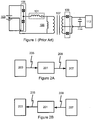
- FIG. 1 a typical SR circuit is shown in Figure 1 .
- a resonant tank 101 consisting of a capacitive element and an inductive element in series receives power from a power source 103 via a switch circuit 105.
- a shunt inductor 106 is placed in parallel across the primary winding of an isolation transformer 107.
- the output of the isolation transformer 107 includes synchronous rectification switching devices 109, which provide output power to a load 113 via a smoothing capacitor 111.
- This type of LLC circuit has the ability to provide output voltage control by operating in either the buck or boost regions. Further, the recent shift in industry standard practice to employ this type of output synchronous rectification has resulted in the capability of providing bidirectional power conversion. It has been discovered that the conventional LLC series resonant circuit has an asymmetric transfer function, where the input to output transfer function (i.e. forward transfer function) is different to the output to input transfer function (i.e. reverse transfer function).
- the reverse transfer function does not facilitate practical reverse power flow control. For example, if the power flow is reversed, the inductive loading provided across the source does not provide any useful function.
- An object of the present invention is to provide a LLC bidirectional resonant converter with improved forward and reverse power flow control or to at least provide the public with a useful choice.
- the present invention aims to overcome, or at least alleviate, some or all of the afore-mentioned problems.
- any integer may be constituted by a single integer or multiple integers.
- the present invention provides a LLC bidirectional resonant converter comprising: a resonant tank, a first switching circuit connected to the resonant tank via first power conduits, a second switching circuit connected to the resonant tank via second power conduits, a switching element, and at least one switchable inductive element which is arranged by the switching element to be in parallel across the second power conduits when operating in a first mode of operation and arranged by the switching element to be in parallel across the first power conduits when operating in a second mode of operation.
- the present invention provides a method of controlling a LLC bidirectional resonant converter comprising the steps of: switching the bidirectional resonant converter between a first mode of operation where the bidirectional resonant converter is arranged to operate in a forward power transfer mode, and a second mode of operation where the bidirectional resonant converter is arranged to operate in a reverse power transfer mode, and controlling a switching element based on the mode of operation in which the bidirectional resonant converter is operating, where the switching element is arranged to connect at least one inductive element in parallel across either first power conduits between a first switching circuit and a resonant tank or second power conduits between the resonant tank and a second switching circuit dependent upon the mode of operation in which the bidirectional resonant converter is operating.
- Figure 2A shows a conceptual diagram of a bidirectional resonant converter operating in a first mode of operation according to this embodiment.
- a resonant tank 201 is connected to a first switch arrangement 203 via a first set of power conduits 205.
- the resonant tank 201 is also connected to a second switch arrangement 207 via a second set of power conduits 209.
- the bidirectional resonant converter is arranged to operate in a forward power transfer mode where the power is transferred in the direction of the arrows indicated in figure 2A , i.e. from the first switch arrangement 203 to the resonant tank 201 and on to the second switch arrangement 207.
- the first switch arrangement 203 controls the power being supplied to the resonant tank and the second switch arrangement 207 operates as a synchronous rectifier.
- Figure 2B shows a conceptual diagram of a bidirectional resonant converter operating in a second mode of operation.
- the resonant tank 201 is still connected to the first switch arrangement 203 via the first set of power conduits 205.
- the resonant tank 201 is also still connected to the second switch arrangement 207 via the second set of power conduits 209.
- the bidirectional resonant converter is arranged to operate in a reverse power transfer mode where the power is transferred in the direction of the arrows indicated in figure 2B , i.e. from the second switch arrangement 207 to the resonant tank 201 and on to the first switch arrangement 203.
- the second switch arrangement 207 controls the power being supplied to the resonant tank and the first switch arrangement 203 operates as a synchronous rectifier.
- Figure 3 shows a circuit block diagram of the bidirectional resonant converter operating in the first mode of operation.
- the resonant tank 201 is shown connected to the first switch arrangement 203.
- a resonant shunt inductor 301 is arranged in parallel across the second set of power conduits. That is, the resonant shunt inductor 301 is effectively arranged in parallel across the second switch arrangement 207.
- Power from a power source 303 is switched by the first switch arrangement 203 to drive the resonant tank 201.
- an isolation transformer 305 is provided to transfer power from the resonant tank to the second switch arrangement.
- the isolation transformer isolates the resonant tank and the first switch arrangement from the second switch arrangement 207 and the load 307.
- the isolation transformer may be an auto transformer if primary to secondary voltage/current transformation is required but isolation is not.
- the second switch arrangement may be connected directly to the resonant circuit.
- Figure 4 shows a circuit block diagram of the bidirectional resonant converter operating in the second mode of operation.
- the bidirectional resonant converter operates in a reverse power transfer mode. Therefore, the original power source 303 becomes a load 311 and the original load 307 becomes the new power source 313.
- a resonant shunt inductor 314 is arranged in parallel across the first set of power conduits. That is, the resonant shunt inductor 314 is effectively arranged in parallel across the first switch arrangement 203. Power from the new power source 313 is switched by the second switch arrangement 207 to drive the resonant tank 201.
- the reverse transfer power is indicated by arrow 315.
- the first switch arrangement 203 is controlled using a first switching sequence.
- the second switch arrangement 207 is controlled using a second switching sequence.
- the first switch arrangement 203 is controlled using a third switching sequence. Further, in this second mode of operation, the second switch arrangement 207 is controlled using a fourth switching sequence.
- first and fourth switching sequences are used to control the amount of power being applied to the resonant tank 201, and the second and third switching sequences are used to synchronise the output of the rectifier circuit.
- Figure 5 shows a circuit diagram of a bidirectional resonant converter according to this embodiment of the present invention.
- a resonant tank 501 includes an inductive element and capacitive element arranged in series.
- a power source 503 provides power to the resonant tank 501 via a first switch arrangement 505.
- the first switch arrangement 505 may be a half bridge arrangement including two MOSFET (Metal Oxide Semiconductor Field Effect Transistor) devices.
- MOSFET Metal Oxide Semiconductor Field Effect Transistor
- IGBT Insulated Gate Bipolar Transistor
- first switch arrangement may be modified to take on the form of a full bridge drive circuit.
- drive circuit may be arranged to employ zero voltage transition (ZVT) switching
- a primary winding on an isolation transformer 507 receives the output from the resonant tank.
- the isolation transformer 507 enables power to be transferred from the resonant tank 501 to the output side of the circuit.
- On the secondary winding side of the isolation transformer 507 is located a half bridge switch arrangement 509 for rectifying the signal output from the isolation transformer.
- the signal output from the isolation transformer is smoothed by a smoothing capacitor 511 and provided to a load 513. It will be understood that, as an alternative, the half bridge switch arrangement may be replaced by a full bridge switch arrangement.
- a single switchable inductive element 515 in the form of a resonant shunt inductor is provided.
- a single-pole single-throw relay switch 517 is provided and controlled to enable the inductive element 515 to be provided across the primary winding of the isolation transformer 507 when the resonant converter is in a first mode of operation, i.e. the inductive element 515 is arranged in parallel across the output of the resonant tank. That is, the resonant shunt inductor is placed in the circuit so that it is parallel across the second set of power conduits 209.
- the inductive element may consist of one or more inductive elements.
- the single-pole single-throw relay switch 517 is controlled to enable the inductive element 515 to be provided across the input of the resonant tank 501.
- the shunt inductor is placed in the circuit so that it is parallel across the first set of power conduits 205.
- the resonant converter in the first mode of operation is arranged to operate in a forward power transfer mode.
- the switchable inductive element 515 provides an effect on the power being transferred through the resonant tank by providing low loss inductive loading on the converter's output, where the converter's output is the second set of power conduits 209.
- the resonant converter is arranged to operate in a reverse power transfer mode.
- the switchable inductive element 515 provides an effect on the power being transferred through the resonant tank by providing a low loss inductive loading on the converter's output, where the converter's output is the first set of power conduits 205.
- a typical value for the switchable inductive element may be chosen based on the desired forward and reverse transfer characteristics for the resonant converter.
- the one or more inductive elements switched across the first set of power conduits may be different components having the same or different values to the one or more inductive elements switched across the second set of power conduits.
- the component values may be chosen to provide independent control of the desired forward and reverse transfer characteristics.
- Figure 6 shows a circuit diagram of a bidirectional resonant converter according to a further embodiment of the present invention.
- first and second switch arrangements are arranged as full bridge switching circuits.
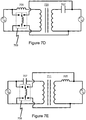
- Figures 7A - 7E show various LC arrangements of the resonant tank for the bidirectional resonant converter according to various further embodiments of the present invention. For example, there may be practical considerations that make it a better choice from a design perspective to locate the inductor and capacitor components of the resonant tank on a particular side of the transformer.
- the LC components of the resonant tank 701 are located on the primary side of the transformer, as described above in the first embodiment.
- the switchable inductive element 703 is arranged so that it may be placed either across the first power conduit or across the second power conduit as indicated in figure 2A and 2B .
- both the LC components of the resonant tank 701 are located on the secondary side of the transformer, along with the switchable inductive element 703.
- the inductive component 705 of the resonant tank is located on the primary side of the transformer 211 and the capacitive component 707 of the resonant tank is located on the secondary side of the transformer.
- the switchable inductive element 709 includes a double-pole double-throw relay that is arranged to position the switchable inductive element either across the second set of power conduits or across the first set of power conduits, where the second set of power conduits is located on the secondary side of the transformer and the first set of power conduits is located on the primary side of the transformer. That is, both ends of the switchable inductive element are switched across the transformer boundary.
- the winding turns ratio of the transformer is 1:1. It will be understood that if the turns ratio is changed from 1:1 then alternative inductive values may be required.
- the capacitive component 707 of the resonant tank is located on the primary side of the transformer 711 and the inductive component 705 of the resonant tank is located on the secondary side of the transformer.
- the switchable inductive element 709 includes a double-pole double-throw relay to position the switchable inductive element either across the second set of power conduits or across the first set of power conduits, where the second set of power conduits is located on the secondary side of the transformer and the first set of power conduits is located on the primary side of the transformer. That is, both ends of the switchable inductive element are switched across the transformer boundary.
- the winding turns ratio of the transformer is 1:1. It will be understood that if the turns ratio is changed from 1:1 then alternative inductive values may be required.
Landscapes
- Engineering & Computer Science (AREA)
- Power Engineering (AREA)
- Dc-Dc Converters (AREA)
- Ac-Ac Conversion (AREA)
Description
- The present invention relates to a LLC bidirectional resonant converter and method of controlling a LLC bidirectional resonant converter. In particular, the present invention relates to a LLC bidirectional resonant converter having an inductive element arranged across a first or second power conduit dependent upon a mode of operation, and method of controlling said LLC bidirectional resonant converter.
- Over the history of development of switched mode power supply systems (SMPS) or resonant converters, the rectifier circuit side of the converter has increased in complexity.
- In traditional resonant SMPS, the rectifier circuit portion of the SMPS included conventional semiconductor diode rectification components, which rectified the voltage signal produced by the resonant tank portion of the converter. In order to control the output voltage of the converter, the frequency at which the resonant tank was switched was varied.
- In order to make this form of converter more efficient, synchronous rectification was introduced. Synchronous rectification involves placing semiconductor switches in parallel with (or replacing) the conventional rectifier diodes. Typically the semiconductor switches are MOSFET (Metal Oxide Semiconductor Field Effect) devices. However the MOSFET devices could be replaced by IGBT (Insulated Gate Bipolar Transistor) devices or a number of alternate devices.
- For example, a typical SR circuit is shown in
Figure 1 . Aresonant tank 101 consisting of a capacitive element and an inductive element in series receives power from apower source 103 via aswitch circuit 105. Ashunt inductor 106 is placed in parallel across the primary winding of anisolation transformer 107. The output of theisolation transformer 107 includes synchronousrectification switching devices 109, which provide output power to aload 113 via a smoothing capacitor 111. - This type of LLC circuit has the ability to provide output voltage control by operating in either the buck or boost regions. Further, the recent shift in industry standard practice to employ this type of output synchronous rectification has resulted in the capability of providing bidirectional power conversion. It has been discovered that the conventional LLC series resonant circuit has an asymmetric transfer function, where the input to output transfer function (i.e. forward transfer function) is different to the output to input transfer function (i.e. reverse transfer function).
- However, it has been found that the reverse transfer function does not facilitate practical reverse power flow control. For example, if the power flow is reversed, the inductive loading provided across the source does not provide any useful function.
- An object of the present invention is to provide a LLC bidirectional resonant converter with improved forward and reverse power flow control or to at least provide the public with a useful choice.
- The present invention aims to overcome, or at least alleviate, some or all of the afore-mentioned problems.
- Further objects and advantages of the invention will be brought out in the following portions of the specification, wherein the detailed description is for the purpose of fully disclosing the preferred embodiment of the invention without placing limitations thereon.
- The background discussion (including any potential prior art) is not to be taken as an admission of the common general knowledge in the art in any country. Any references discussed state the assertions of the author of those references and not the assertions of the applicant of this application. As such, the applicant reserves the right to challenge the accuracy and relevance of the references discussed.
- It is acknowledged that the terms "comprise", "comprises" and "comprising" may, under varying jurisdictions, be attributed with either an exclusive or an inclusive meaning. For the purpose of this specification, and unless otherwise noted, these terms are intended to have an inclusive meaning - i.e. they will be taken to mean an inclusion of the listed components that the use directly references, but optionally also the inclusion of other non-specified components or elements. It will be understood that this intended meaning also similarly applies to the terms mentioned when used to define steps in a method or process.
- It will be understood that, when describing various integers, such as modules, components, elements etc., any integer may be constituted by a single integer or multiple integers.
- According to one aspect, the present invention provides a LLC bidirectional resonant converter comprising: a resonant tank, a first switching circuit connected to the resonant tank via first power conduits, a second switching circuit connected to the resonant tank via second power conduits, a switching element, and at least one switchable inductive element which is arranged by the switching element to be in parallel across the second power conduits when operating in a first mode of operation and arranged by the switching element to be in parallel across the first power conduits when operating in a second mode of operation.
- According to second aspect, the present invention provides a method of controlling a LLC bidirectional resonant converter comprising the steps of: switching the bidirectional resonant converter between a first mode of operation where the bidirectional resonant converter is arranged to operate in a forward power transfer mode, and a second mode of operation where the bidirectional resonant converter is arranged to operate in a reverse power transfer mode, and controlling a switching element based on the mode of operation in which the bidirectional resonant converter is operating, where the switching element is arranged to connect at least one inductive element in parallel across either first power conduits between a first switching circuit and a resonant tank or second power conduits between the resonant tank and a second switching circuit dependent upon the mode of operation in which the bidirectional resonant converter is operating.
- Embodiments of the present invention will now be described, by way of example only, with reference to the accompanying drawings, in which:
-
Figure 1 shows a known resonant converter circuit; -
Figure 2A shows a conceptual diagram of a bidirectional resonant converter operating in a first mode of operation according to an embodiment of the present invention; -
Figure 2B shows a conceptual diagram of a bidirectional resonant converter operating in a second mode of operation according to an embodiment of the present invention; -
Figure 3 shows a block circuit diagram of a bidirectional resonant converter operating in a first mode of operation according to an embodiment of the present invention; -
Figure 4 shows a block circuit diagram of a bidirectional resonant converter operating in a second mode of operation according to an embodiment of the present invention; -
Figure 5 shows a circuit diagram of a bidirectional resonant converter according to an embodiment of the present invention; -
Figure 6 shows a circuit diagram of a bidirectional resonant converter according to an embodiment of the present invention; -
Figure 7A shows a configuration diagram of a bidirectional resonant converter according to an embodiment of the present invention; -
Figure 7B shows a configuration diagram of a bidirectional resonant converter according to an embodiment of the present invention; -
Figure 7C shows a configuration diagram of a bidirectional resonant converter according to an embodiment of the present invention; -
Figure 7D shows a configuration diagram of a bidirectional resonant converter according to an embodiment of the present invention; and -
Figure 7E shows a configuration diagram of a bidirectional resonant converter according to an embodiment of the present invention. -
Figure 2A shows a conceptual diagram of a bidirectional resonant converter operating in a first mode of operation according to this embodiment. - A
resonant tank 201 is connected to afirst switch arrangement 203 via a first set ofpower conduits 205. Theresonant tank 201 is also connected to asecond switch arrangement 207 via a second set ofpower conduits 209. - In a first mode of operation, the bidirectional resonant converter is arranged to operate in a forward power transfer mode where the power is transferred in the direction of the arrows indicated in
figure 2A , i.e. from thefirst switch arrangement 203 to theresonant tank 201 and on to thesecond switch arrangement 207. When the resonant converter is operated in the first mode, thefirst switch arrangement 203 controls the power being supplied to the resonant tank and thesecond switch arrangement 207 operates as a synchronous rectifier.Figure 2B shows a conceptual diagram of a bidirectional resonant converter operating in a second mode of operation. - The
resonant tank 201 is still connected to thefirst switch arrangement 203 via the first set ofpower conduits 205. Theresonant tank 201 is also still connected to thesecond switch arrangement 207 via the second set ofpower conduits 209. However, in this second mode of operation, the bidirectional resonant converter is arranged to operate in a reverse power transfer mode where the power is transferred in the direction of the arrows indicated infigure 2B , i.e. from thesecond switch arrangement 207 to theresonant tank 201 and on to thefirst switch arrangement 203. When the converter is placed in this second mode, thesecond switch arrangement 207 controls the power being supplied to the resonant tank and thefirst switch arrangement 203 operates as a synchronous rectifier. -
Figure 3 shows a circuit block diagram of the bidirectional resonant converter operating in the first mode of operation. - The
resonant tank 201 is shown connected to thefirst switch arrangement 203. Aresonant shunt inductor 301 is arranged in parallel across the second set of power conduits. That is, theresonant shunt inductor 301 is effectively arranged in parallel across thesecond switch arrangement 207. Power from apower source 303 is switched by thefirst switch arrangement 203 to drive theresonant tank 201. - According to this embodiment, an
isolation transformer 305 is provided to transfer power from the resonant tank to the second switch arrangement. The isolation transformer isolates the resonant tank and the first switch arrangement from thesecond switch arrangement 207 and theload 307. It will be understood however that, as an alternative, the isolation transformer may be an auto transformer if primary to secondary voltage/current transformation is required but isolation is not. As a further alternative, if primary to secondary voltage/current transformation is not required, the second switch arrangement may be connected directly to the resonant circuit. - The forward transfer of power is indicated by
arrow 309. -
Figure 4 shows a circuit block diagram of the bidirectional resonant converter operating in the second mode of operation. - In this second mode of operation, the bidirectional resonant converter operates in a reverse power transfer mode. Therefore, the
original power source 303 becomes aload 311 and theoriginal load 307 becomes thenew power source 313. Aresonant shunt inductor 314 is arranged in parallel across the first set of power conduits. That is, theresonant shunt inductor 314 is effectively arranged in parallel across thefirst switch arrangement 203. Power from thenew power source 313 is switched by thesecond switch arrangement 207 to drive theresonant tank 201. - The reverse transfer power is indicated by
arrow 315. - As shown in
figure 3 , in the first mode of operation, thefirst switch arrangement 203 is controlled using a first switching sequence. Further, in this first mode of operation, thesecond switch arrangement 207 is controlled using a second switching sequence. - As shown in
figure 4 , in the second mode of operation, thefirst switch arrangement 203 is controlled using a third switching sequence. Further, in this second mode of operation, thesecond switch arrangement 207 is controlled using a fourth switching sequence. - It will be understood that the first and fourth switching sequences are used to control the amount of power being applied to the
resonant tank 201, and the second and third switching sequences are used to synchronise the output of the rectifier circuit. -
Figure 5 shows a circuit diagram of a bidirectional resonant converter according to this embodiment of the present invention. - A
resonant tank 501 includes an inductive element and capacitive element arranged in series. Apower source 503 provides power to theresonant tank 501 via afirst switch arrangement 505. - According to this embodiment, the
first switch arrangement 505 may be a half bridge arrangement including two MOSFET (Metal Oxide Semiconductor Field Effect Transistor) devices. - It will be understood that alternative devices may be used for synchronous rectification such as IGBT (Insulated Gate Bipolar Transistor) devices or a number of alternate devices.
- It will also be understood that the first switch arrangement may be modified to take on the form of a full bridge drive circuit. Further, the drive circuit may be arranged to employ zero voltage transition (ZVT) switching
- A primary winding on an
isolation transformer 507 receives the output from the resonant tank. Theisolation transformer 507 enables power to be transferred from theresonant tank 501 to the output side of the circuit. On the secondary winding side of theisolation transformer 507 is located a halfbridge switch arrangement 509 for rectifying the signal output from the isolation transformer. The signal output from the isolation transformer is smoothed by a smoothing capacitor 511 and provided to aload 513. It will be understood that, as an alternative, the half bridge switch arrangement may be replaced by a full bridge switch arrangement. - According to this embodiment, a single switchable
inductive element 515 in the form of a resonant shunt inductor is provided. A single-pole single-throw relay switch 517 is provided and controlled to enable theinductive element 515 to be provided across the primary winding of theisolation transformer 507 when the resonant converter is in a first mode of operation, i.e. theinductive element 515 is arranged in parallel across the output of the resonant tank. That is, the resonant shunt inductor is placed in the circuit so that it is parallel across the second set ofpower conduits 209. - It will be understood that the inductive element may consist of one or more inductive elements.
- In a second mode of operation, the single-pole single-
throw relay switch 517 is controlled to enable theinductive element 515 to be provided across the input of theresonant tank 501. Referring tofigure 2A and 2B , the shunt inductor is placed in the circuit so that it is parallel across the first set ofpower conduits 205. - Therefore, in the first mode of operation the resonant converter is arranged to operate in a forward power transfer mode. The switchable
inductive element 515 provides an effect on the power being transferred through the resonant tank by providing low loss inductive loading on the converter's output, where the converter's output is the second set ofpower conduits 209. - In a second mode of operation, the resonant converter is arranged to operate in a reverse power transfer mode. The switchable
inductive element 515 provides an effect on the power being transferred through the resonant tank by providing a low loss inductive loading on the converter's output, where the converter's output is the first set ofpower conduits 205. - It will be understood that a typical value for the switchable inductive element may be chosen based on the desired forward and reverse transfer characteristics for the resonant converter.
- Further, it will be understood that, as an alternative, the one or more inductive elements switched across the first set of power conduits may be different components having the same or different values to the one or more inductive elements switched across the second set of power conduits. In this manner the component values may be chosen to provide independent control of the desired forward and reverse transfer characteristics.
-
Figure 6 shows a circuit diagram of a bidirectional resonant converter according to a further embodiment of the present invention. - According to this further embodiment, a similar arrangement in terms of a
resonant tank 601,power source 603,first switch arrangement 605,isolation transformer 607 andsecond switch arrangement 609 is provided. However, according to this embodiment, the first and second switch arrangements are arranged as full bridge switching circuits. -
Figures 7A - 7E show various LC arrangements of the resonant tank for the bidirectional resonant converter according to various further embodiments of the present invention. For example, there may be practical considerations that make it a better choice from a design perspective to locate the inductor and capacitor components of the resonant tank on a particular side of the transformer. - According to
figure 7A , it can be seen that the LC components of theresonant tank 701 are located on the primary side of the transformer, as described above in the first embodiment. The switchableinductive element 703 is arranged so that it may be placed either across the first power conduit or across the second power conduit as indicated infigure 2A and 2B . - According to
figure 7B , both the LC components of theresonant tank 701 are located on the secondary side of the transformer, along with the switchableinductive element 703. - According to
figure 7C , a non-isolated version of the converter is shown, where no transformer is provided to separate the input side form the output side. - According to
figure 7D , theinductive component 705 of the resonant tank is located on the primary side of the transformer 211 and thecapacitive component 707 of the resonant tank is located on the secondary side of the transformer. The switchableinductive element 709 includes a double-pole double-throw relay that is arranged to position the switchable inductive element either across the second set of power conduits or across the first set of power conduits, where the second set of power conduits is located on the secondary side of the transformer and the first set of power conduits is located on the primary side of the transformer. That is, both ends of the switchable inductive element are switched across the transformer boundary. According to this example, the winding turns ratio of the transformer is 1:1. It will be understood that if the turns ratio is changed from 1:1 then alternative inductive values may be required. - According to
figure 7E , thecapacitive component 707 of the resonant tank is located on the primary side of thetransformer 711 and theinductive component 705 of the resonant tank is located on the secondary side of the transformer. The switchableinductive element 709 includes a double-pole double-throw relay to position the switchable inductive element either across the second set of power conduits or across the first set of power conduits, where the second set of power conduits is located on the secondary side of the transformer and the first set of power conduits is located on the primary side of the transformer. That is, both ends of the switchable inductive element are switched across the transformer boundary. According to this example, the winding turns ratio of the transformer is 1:1. It will be understood that if the turns ratio is changed from 1:1 then alternative inductive values may be required. - It will be understood that the embodiments of the present invention described herein are by way of example only, and that various changes and modifications may be made without departing from the scope of invention.
Claims (15)
- A LLC bidirectional resonant converter comprising:a resonant tank,a first switching circuit connected to the resonant tank via first power conduits, a second switching circuit connected to the resonant tank via second power conduits,a switching element, andat least one switchable inductive element which is arranged by the switching element to be in parallel across the second power conduits when operating in a first mode of operation where the bidirectional resonant converter is arranged to operate in a forward power transfer mode and arranged by the switching element to be in parallel across the first power conduits when operating in a second mode of operation where the bidirectional resonant converter is arranged to operate in a reverse power transfer mode.
- The bidirectional resonant converter of claim 1, wherein, when operating the bidirectional resonant converter in the first mode of operation, power is transferred from the first switching circuit via the first power conduits to the resonant tank, and from the resonant tank via the second power conduits to the second switching circuit, and when operating the bidirectional resonant converter in the second mode of operation, power is transferred from the second switching circuit via the second power conduits to the resonant tank, and from the resonant tank via the first power conduits to the first switching circuit.
- The bidirectional resonant converter of claim 1, wherein,
when operating the bidirectional resonant converter in the first mode of operation, the first switching circuit is arranged to switch according to a first switching sequence and the second switching circuit is arranged to switch according to a second switching sequence, when operating the bidirectional resonant converter in a second mode of operation, the first switching circuit is arranged to switch according to a third switching sequence and the second switching circuit is arranged to switch according to a fourth switching sequence. - The bidirectional resonant converter of claim 1, wherein the resonant tank comprises a resonant capacitive element in series with a resonant inductive element.
- The bidirectional resonant converter of claim 1, wherein, in the first mode of operation, the bidirectional resonant converter operates in a forward power transfer mode and in a second mode of operation the bidirectional resonant converter operates in a reverse power transfer mode.
- The bidirectional resonant converter of claim 3, wherein the second switching circuit is arranged to be a first rectifier circuit during the first mode of operation; and preferably wherein the first rectifier circuit is a first synchronous rectifier circuit that is switched according to the second switching sequence.
- The bidirectional resonant converter of claim 6, wherein the first switching circuit is arranged to be a second rectifier circuit during the second mode of operation; and preferably wherein the second rectifier circuit is a
< second synchronous rectifier circuit that is switched according to the fourth switching sequence. - The bidirectional resonant converter of claim 1 further comprising a transformer arranged between the resonant tank and the second switching circuit.
- The bidirectional resonant converter of claim 1 further comprising a transformer arranged between the first switching circuit and the resonant tank.
- The bidirectional resonant converter of claim 8 or 9, wherein the transformer is one of an isolation transformer and an auto transformer.
- The bidirectional resonant converter of claim 8 or 9, wherein the resonant tank includes a resonant capacitive element in series with a resonant inductive element.
- The bidirectional resonant converter of claim 11, wherein the resonant capacitive element and resonant inductive element are in series on a primary side of the transformer; or
wherein the resonant capacitive element and resonant inductive element are in series on a secondary side of the transformer; or
wherein the resonant inductive element is on a primary side of the transformer and the resonant capacitive element is in series on a secondary side of the transformer; or
wherein the resonant inductive element is on a secondary side of the transformer and the resonant capacitive element is in series on a primary side of the transformer. - The bidirectional resonant converter of claim 1, wherein the first and/or second switching circuit is arranged as a half bridge drive circuit; or
wherein the first and/or second switching circuit is arranged as a full bridge drive circuit. - The bidirectional resonant converter of claim 1, wherein the first and/or second switching circuit is arranged as a push-pull drive circuit; or
wherein the first and/or second switching circuit employs ZVT switching. - A method of controlling a LLC bidirectional resonant converter comprising the steps of:switching the bidirectional resonant converter between a first mode of operation where the bidirectional resonant converter is arranged to operate in a forward power transfer mode, and a second mode of operation where the bidirectional resonant converter is arranged to operate in a reverse power transfer mode, and controlling a switching element based on the mode of operation in which the bidirectional resonant converter is operating, where the switching element is arranged to connect at least one inductive element in parallel across either first power conduits between a first switching circuit and a resonant tank or second power conduits between the resonant tank and a second switching circuit dependent upon the mode of operation in which the bidirectional resonant converter is operating.
Applications Claiming Priority (2)
| Application Number | Priority Date | Filing Date | Title |
|---|---|---|---|
| NZ59728811 | 2011-12-21 | ||
| PCT/NZ2012/000017 WO2013095161A2 (en) | 2011-12-21 | 2012-02-20 | Llc bidirectional resonant converter and method of controlling |
Publications (2)
| Publication Number | Publication Date |
|---|---|
| EP2795781A2 EP2795781A2 (en) | 2014-10-29 |
| EP2795781B1 true EP2795781B1 (en) | 2017-02-01 |
Family
ID=48669670
Family Applications (1)
| Application Number | Title | Priority Date | Filing Date |
|---|---|---|---|
| EP12858772.2A Not-in-force EP2795781B1 (en) | 2011-12-21 | 2012-02-20 | Llc bidirectional resonant converter and method of controlling |
Country Status (3)
| Country | Link |
|---|---|
| US (1) | US9509223B2 (en) |
| EP (1) | EP2795781B1 (en) |
| WO (1) | WO2013095161A2 (en) |
Cited By (2)
| Publication number | Priority date | Publication date | Assignee | Title |
|---|---|---|---|---|
| CN109361321A (en) * | 2018-11-29 | 2019-02-19 | 西安交通大学 | A reverse working circuit and design method of LLC resonant converter |
| EP4525289A1 (en) | 2023-09-14 | 2025-03-19 | FRONIUS INTERNATIONAL GmbH | Resonant converter with parallel input half-bridges and method for controlling a resonant converter |
Families Citing this family (13)
| Publication number | Priority date | Publication date | Assignee | Title |
|---|---|---|---|---|
| CN104811049B (en) * | 2014-01-29 | 2017-11-21 | 艾默生网络能源有限公司 | A kind of resonance circuit |
| CN105024551A (en) * | 2014-04-16 | 2015-11-04 | 艾默生网络能源有限公司 | Resonance circuit, charger and uninterrupted power supply |
| CN105024552A (en) * | 2014-04-16 | 2015-11-04 | 艾默生网络能源有限公司 | Resonance circuit, charger and uninterrupted power supply |
| CN105099197A (en) * | 2014-05-20 | 2015-11-25 | 艾默生网络能源有限公司 | Resonance circuit, charger and uninterruptible power supply |
| CN104022658B (en) * | 2014-06-16 | 2017-10-27 | 南京航空航天大学 | A kind of high reliability is two-tube to recommend LLC resonant converter |
| US9787117B2 (en) | 2015-09-17 | 2017-10-10 | Conductive Holding, LLC | Bidirectional battery charger integrated with renewable energy generation |
| US10560024B2 (en) | 2015-09-17 | 2020-02-11 | Conductive Holding, LLC | Bidirectional DC/DC converter for a charging system |
| GB201602044D0 (en) | 2016-02-04 | 2016-03-23 | Eltek As | Bidirectional DC-DC resonant converter |
| CN106100148B (en) * | 2016-06-15 | 2018-08-28 | 东南大学 | A kind of bidirectional radio energy Transmission system energy flow direction-controlling method based on structure changes |
| FR3076123B1 (en) * | 2017-12-21 | 2021-01-08 | Renault Sas | DC-DC CONVERTER FOR BIDIRECTIONAL CHARGER. |
| FR3089076B1 (en) * | 2018-11-22 | 2021-10-29 | Renault Sas | LLC type direct current - resonant direct current converter |
| US12068711B2 (en) * | 2021-02-03 | 2024-08-20 | Toyota Motor Engineering & Manufacturing North America, Inc. | High frequency AC power distribution network for electric vehicles |
| CN114123801B (en) * | 2022-01-25 | 2022-04-22 | 常州索维尔电子科技有限公司 | Control method and control device of boost circuit based on LLC circuit |
Family Cites Families (4)
| Publication number | Priority date | Publication date | Assignee | Title |
|---|---|---|---|---|
| US5388040A (en) | 1993-09-30 | 1995-02-07 | Hughes Aircraft Company | Series resonant converter having an actively controlled third element |
| TWI309498B (en) * | 2006-06-09 | 2009-05-01 | Delta Electronics Inc | Resonant converter and voltage stabilizing method thereof |
| US7742318B2 (en) * | 2008-06-10 | 2010-06-22 | Virginia Tech Intellectual Properties, Inc. | Multi-element resonant converters |
| US9059636B2 (en) * | 2010-02-18 | 2015-06-16 | Peter Waldemar Lehn | DC-DC converter circuit using LLC circuit in the region of voltage gain above unity |
-
2012
- 2012-02-20 EP EP12858772.2A patent/EP2795781B1/en not_active Not-in-force
- 2012-02-20 US US14/368,187 patent/US9509223B2/en not_active Expired - Fee Related
- 2012-02-20 WO PCT/NZ2012/000017 patent/WO2013095161A2/en not_active Ceased
Cited By (4)
| Publication number | Priority date | Publication date | Assignee | Title |
|---|---|---|---|---|
| CN109361321A (en) * | 2018-11-29 | 2019-02-19 | 西安交通大学 | A reverse working circuit and design method of LLC resonant converter |
| CN109361321B (en) * | 2018-11-29 | 2019-10-11 | 西安交通大学 | A reverse working circuit and design method of LLC resonant converter |
| EP4525289A1 (en) | 2023-09-14 | 2025-03-19 | FRONIUS INTERNATIONAL GmbH | Resonant converter with parallel input half-bridges and method for controlling a resonant converter |
| WO2025056201A1 (en) | 2023-09-14 | 2025-03-20 | Fronius International Gmbh | Resonant converter with parallel input half-bridges and method for controlling a resonant converter |
Also Published As
| Publication number | Publication date |
|---|---|
| EP2795781A2 (en) | 2014-10-29 |
| WO2013095161A2 (en) | 2013-06-27 |
| WO2013095161A3 (en) | 2013-11-28 |
| US9509223B2 (en) | 2016-11-29 |
| US20140347893A1 (en) | 2014-11-27 |
| CN104011986A (en) | 2014-08-27 |
Similar Documents
| Publication | Publication Date | Title |
|---|---|---|
| EP2795781B1 (en) | Llc bidirectional resonant converter and method of controlling | |
| US8542501B2 (en) | Switching power-supply apparatus | |
| US8780585B2 (en) | Double phase-shifting full-bridge DC-to-DC converter | |
| US10622907B2 (en) | DC-DC converter | |
| US8111052B2 (en) | Zero voltage switching | |
| KR101395487B1 (en) | Dc-dc converter | |
| US20190157978A1 (en) | Multi-phase llc converters connected in parallel and series | |
| US20150117068A1 (en) | Drive circuit for synchronous rectifier and method thereof | |
| US9570981B2 (en) | Bidirectional DC-DC converter | |
| KR20160056155A (en) | Power converter | |
| CN104953843A (en) | Resonance DC/DC converter | |
| JP7637428B2 (en) | Direct Power Converter | |
| JP6107848B2 (en) | Bidirectional DC / DC converter | |
| US20100054008A1 (en) | Inductorless Isolated Power Converters With Zero Voltage and Zero Current Switching | |
| KR102211454B1 (en) | Isolated DC-DC converter and driving method thereof | |
| US20150117061A1 (en) | Power supply apparatus | |
| KR20160101808A (en) | Full-Bridge DC-DC Converter | |
| US11664721B2 (en) | Multiphase interleaved forward power converters including clamping circuits | |
| JP2018014852A (en) | Insulated dc/dc converter | |
| US20120281435A1 (en) | Dc-dc converter | |
| KR101688790B1 (en) | Double step-down dc-dc converter and control method thereof | |
| CN104011986B (en) | LLC bidirectional resonant converter and control method | |
| KR102572123B1 (en) | Multimode converter with soft switching | |
| Rehlaender et al. | Interleaved Active Clamp Forward Converters as Single Stage On-Board DC-DC Converters for EVs-an Accurate Model and Design Considerations | |
| JP2020022307A (en) | Power supply device and method of controlling the same |
Legal Events
| Date | Code | Title | Description |
|---|---|---|---|
| PUAI | Public reference made under article 153(3) epc to a published international application that has entered the european phase |
Free format text: ORIGINAL CODE: 0009012 |
|
| 17P | Request for examination filed |
Effective date: 20140623 |
|
| AK | Designated contracting states |
Kind code of ref document: A2 Designated state(s): AL AT BE BG CH CY CZ DE DK EE ES FI FR GB GR HR HU IE IS IT LI LT LU LV MC MK MT NL NO PL PT RO RS SE SI SK SM TR |
|
| DAX | Request for extension of the european patent (deleted) | ||
| GRAP | Despatch of communication of intention to grant a patent |
Free format text: ORIGINAL CODE: EPIDOSNIGR1 |
|
| INTG | Intention to grant announced |
Effective date: 20160810 |
|
| GRAS | Grant fee paid |
Free format text: ORIGINAL CODE: EPIDOSNIGR3 |
|
| GRAA | (expected) grant |
Free format text: ORIGINAL CODE: 0009210 |
|
| AK | Designated contracting states |
Kind code of ref document: B1 Designated state(s): AL AT BE BG CH CY CZ DE DK EE ES FI FR GB GR HR HU IE IS IT LI LT LU LV MC MK MT NL NO PL PT RO RS SE SI SK SM TR |
|
| REG | Reference to a national code |
Ref country code: GB Ref legal event code: FG4D |
|
| REG | Reference to a national code |
Ref country code: CH Ref legal event code: EP Ref country code: AT Ref legal event code: REF Ref document number: 866315 Country of ref document: AT Kind code of ref document: T Effective date: 20170215 |
|
| REG | Reference to a national code |
Ref country code: IE Ref legal event code: FG4D |
|
| REG | Reference to a national code |
Ref country code: FR Ref legal event code: PLFP Year of fee payment: 6 |
|
| REG | Reference to a national code |
Ref country code: DE Ref legal event code: R096 Ref document number: 602012028459 Country of ref document: DE |
|
| REG | Reference to a national code |
Ref country code: NL Ref legal event code: MP Effective date: 20170201 |
|
| REG | Reference to a national code |
Ref country code: LT Ref legal event code: MG4D |
|
| REG | Reference to a national code |
Ref country code: AT Ref legal event code: MK05 Ref document number: 866315 Country of ref document: AT Kind code of ref document: T Effective date: 20170201 |
|
| PG25 | Lapsed in a contracting state [announced via postgrant information from national office to epo] |
Ref country code: LT Free format text: LAPSE BECAUSE OF FAILURE TO SUBMIT A TRANSLATION OF THE DESCRIPTION OR TO PAY THE FEE WITHIN THE PRESCRIBED TIME-LIMIT Effective date: 20170201 Ref country code: IS Free format text: LAPSE BECAUSE OF FAILURE TO SUBMIT A TRANSLATION OF THE DESCRIPTION OR TO PAY THE FEE WITHIN THE PRESCRIBED TIME-LIMIT Effective date: 20170601 Ref country code: HR Free format text: LAPSE BECAUSE OF FAILURE TO SUBMIT A TRANSLATION OF THE DESCRIPTION OR TO PAY THE FEE WITHIN THE PRESCRIBED TIME-LIMIT Effective date: 20170201 Ref country code: GR Free format text: LAPSE BECAUSE OF FAILURE TO SUBMIT A TRANSLATION OF THE DESCRIPTION OR TO PAY THE FEE WITHIN THE PRESCRIBED TIME-LIMIT Effective date: 20170502 Ref country code: NO Free format text: LAPSE BECAUSE OF FAILURE TO SUBMIT A TRANSLATION OF THE DESCRIPTION OR TO PAY THE FEE WITHIN THE PRESCRIBED TIME-LIMIT Effective date: 20170501 Ref country code: FI Free format text: LAPSE BECAUSE OF FAILURE TO SUBMIT A TRANSLATION OF THE DESCRIPTION OR TO PAY THE FEE WITHIN THE PRESCRIBED TIME-LIMIT Effective date: 20170201 |
|
| PG25 | Lapsed in a contracting state [announced via postgrant information from national office to epo] |
Ref country code: BG Free format text: LAPSE BECAUSE OF FAILURE TO SUBMIT A TRANSLATION OF THE DESCRIPTION OR TO PAY THE FEE WITHIN THE PRESCRIBED TIME-LIMIT Effective date: 20170501 Ref country code: ES Free format text: LAPSE BECAUSE OF FAILURE TO SUBMIT A TRANSLATION OF THE DESCRIPTION OR TO PAY THE FEE WITHIN THE PRESCRIBED TIME-LIMIT Effective date: 20170201 Ref country code: PT Free format text: LAPSE BECAUSE OF FAILURE TO SUBMIT A TRANSLATION OF THE DESCRIPTION OR TO PAY THE FEE WITHIN THE PRESCRIBED TIME-LIMIT Effective date: 20170601 Ref country code: SE Free format text: LAPSE BECAUSE OF FAILURE TO SUBMIT A TRANSLATION OF THE DESCRIPTION OR TO PAY THE FEE WITHIN THE PRESCRIBED TIME-LIMIT Effective date: 20170201 Ref country code: RS Free format text: LAPSE BECAUSE OF FAILURE TO SUBMIT A TRANSLATION OF THE DESCRIPTION OR TO PAY THE FEE WITHIN THE PRESCRIBED TIME-LIMIT Effective date: 20170201 Ref country code: AT Free format text: LAPSE BECAUSE OF FAILURE TO SUBMIT A TRANSLATION OF THE DESCRIPTION OR TO PAY THE FEE WITHIN THE PRESCRIBED TIME-LIMIT Effective date: 20170201 Ref country code: PL Free format text: LAPSE BECAUSE OF FAILURE TO SUBMIT A TRANSLATION OF THE DESCRIPTION OR TO PAY THE FEE WITHIN THE PRESCRIBED TIME-LIMIT Effective date: 20170201 Ref country code: NL Free format text: LAPSE BECAUSE OF FAILURE TO SUBMIT A TRANSLATION OF THE DESCRIPTION OR TO PAY THE FEE WITHIN THE PRESCRIBED TIME-LIMIT Effective date: 20170201 Ref country code: LV Free format text: LAPSE BECAUSE OF FAILURE TO SUBMIT A TRANSLATION OF THE DESCRIPTION OR TO PAY THE FEE WITHIN THE PRESCRIBED TIME-LIMIT Effective date: 20170201 |
|
| REG | Reference to a national code |
Ref country code: CH Ref legal event code: PL |
|
| PG25 | Lapsed in a contracting state [announced via postgrant information from national office to epo] |
Ref country code: SK Free format text: LAPSE BECAUSE OF FAILURE TO SUBMIT A TRANSLATION OF THE DESCRIPTION OR TO PAY THE FEE WITHIN THE PRESCRIBED TIME-LIMIT Effective date: 20170201 Ref country code: CH Free format text: LAPSE BECAUSE OF NON-PAYMENT OF DUE FEES Effective date: 20170228 Ref country code: EE Free format text: LAPSE BECAUSE OF FAILURE TO SUBMIT A TRANSLATION OF THE DESCRIPTION OR TO PAY THE FEE WITHIN THE PRESCRIBED TIME-LIMIT Effective date: 20170201 Ref country code: RO Free format text: LAPSE BECAUSE OF FAILURE TO SUBMIT A TRANSLATION OF THE DESCRIPTION OR TO PAY THE FEE WITHIN THE PRESCRIBED TIME-LIMIT Effective date: 20170201 Ref country code: CZ Free format text: LAPSE BECAUSE OF FAILURE TO SUBMIT A TRANSLATION OF THE DESCRIPTION OR TO PAY THE FEE WITHIN THE PRESCRIBED TIME-LIMIT Effective date: 20170201 Ref country code: IT Free format text: LAPSE BECAUSE OF FAILURE TO SUBMIT A TRANSLATION OF THE DESCRIPTION OR TO PAY THE FEE WITHIN THE PRESCRIBED TIME-LIMIT Effective date: 20170201 Ref country code: LI Free format text: LAPSE BECAUSE OF NON-PAYMENT OF DUE FEES Effective date: 20170228 |
|
| REG | Reference to a national code |
Ref country code: DE Ref legal event code: R097 Ref document number: 602012028459 Country of ref document: DE |
|
| REG | Reference to a national code |
Ref country code: IE Ref legal event code: MM4A |
|
| PG25 | Lapsed in a contracting state [announced via postgrant information from national office to epo] |
Ref country code: SM Free format text: LAPSE BECAUSE OF FAILURE TO SUBMIT A TRANSLATION OF THE DESCRIPTION OR TO PAY THE FEE WITHIN THE PRESCRIBED TIME-LIMIT Effective date: 20170201 Ref country code: DK Free format text: LAPSE BECAUSE OF FAILURE TO SUBMIT A TRANSLATION OF THE DESCRIPTION OR TO PAY THE FEE WITHIN THE PRESCRIBED TIME-LIMIT Effective date: 20170201 Ref country code: MC Free format text: LAPSE BECAUSE OF FAILURE TO SUBMIT A TRANSLATION OF THE DESCRIPTION OR TO PAY THE FEE WITHIN THE PRESCRIBED TIME-LIMIT Effective date: 20170201 |
|
| PLBE | No opposition filed within time limit |
Free format text: ORIGINAL CODE: 0009261 |
|
| STAA | Information on the status of an ep patent application or granted ep patent |
Free format text: STATUS: NO OPPOSITION FILED WITHIN TIME LIMIT |
|
| PG25 | Lapsed in a contracting state [announced via postgrant information from national office to epo] |
Ref country code: LU Free format text: LAPSE BECAUSE OF NON-PAYMENT OF DUE FEES Effective date: 20170220 |
|
| 26N | No opposition filed |
Effective date: 20171103 |
|
| REG | Reference to a national code |
Ref country code: FR Ref legal event code: PLFP Year of fee payment: 7 |
|
| REG | Reference to a national code |
Ref country code: BE Ref legal event code: MM Effective date: 20170228 |
|
| PG25 | Lapsed in a contracting state [announced via postgrant information from national office to epo] |
Ref country code: SI Free format text: LAPSE BECAUSE OF FAILURE TO SUBMIT A TRANSLATION OF THE DESCRIPTION OR TO PAY THE FEE WITHIN THE PRESCRIBED TIME-LIMIT Effective date: 20170201 Ref country code: IE Free format text: LAPSE BECAUSE OF NON-PAYMENT OF DUE FEES Effective date: 20170220 |
|
| PG25 | Lapsed in a contracting state [announced via postgrant information from national office to epo] |
Ref country code: BE Free format text: LAPSE BECAUSE OF NON-PAYMENT OF DUE FEES Effective date: 20170228 |
|
| PG25 | Lapsed in a contracting state [announced via postgrant information from national office to epo] |
Ref country code: MT Free format text: LAPSE BECAUSE OF NON-PAYMENT OF DUE FEES Effective date: 20170220 |
|
| REG | Reference to a national code |
Ref country code: GB Ref legal event code: 732E Free format text: REGISTERED BETWEEN 20181108 AND 20181114 |
|
| REG | Reference to a national code |
Ref country code: DE Ref legal event code: R082 Ref document number: 602012028459 Country of ref document: DE Ref country code: DE Ref legal event code: R081 Ref document number: 602012028459 Country of ref document: DE Owner name: EATON INTELLIGENT POWER LIMITED, IE Free format text: FORMER OWNER: EATON INDUSTRIES COMPANY, CHRISTCHURCH, NZ Ref country code: DE Ref legal event code: R082 Ref document number: 602012028459 Country of ref document: DE Representative=s name: WAGNER & GEYER PARTNERSCHAFT MBB PATENT- UND R, DE |
|
| REG | Reference to a national code |
Ref country code: DE Ref legal event code: R082 Ref document number: 602012028459 Country of ref document: DE Representative=s name: WAGNER & GEYER PARTNERSCHAFT MBB PATENT- UND R, DE |
|
| PG25 | Lapsed in a contracting state [announced via postgrant information from national office to epo] |
Ref country code: HU Free format text: LAPSE BECAUSE OF FAILURE TO SUBMIT A TRANSLATION OF THE DESCRIPTION OR TO PAY THE FEE WITHIN THE PRESCRIBED TIME-LIMIT; INVALID AB INITIO Effective date: 20120220 |
|
| PG25 | Lapsed in a contracting state [announced via postgrant information from national office to epo] |
Ref country code: CY Free format text: LAPSE BECAUSE OF FAILURE TO SUBMIT A TRANSLATION OF THE DESCRIPTION OR TO PAY THE FEE WITHIN THE PRESCRIBED TIME-LIMIT Effective date: 20170201 |
|
| PG25 | Lapsed in a contracting state [announced via postgrant information from national office to epo] |
Ref country code: MK Free format text: LAPSE BECAUSE OF FAILURE TO SUBMIT A TRANSLATION OF THE DESCRIPTION OR TO PAY THE FEE WITHIN THE PRESCRIBED TIME-LIMIT Effective date: 20170201 |
|
| PG25 | Lapsed in a contracting state [announced via postgrant information from national office to epo] |
Ref country code: TR Free format text: LAPSE BECAUSE OF FAILURE TO SUBMIT A TRANSLATION OF THE DESCRIPTION OR TO PAY THE FEE WITHIN THE PRESCRIBED TIME-LIMIT Effective date: 20170201 |
|
| PG25 | Lapsed in a contracting state [announced via postgrant information from national office to epo] |
Ref country code: AL Free format text: LAPSE BECAUSE OF FAILURE TO SUBMIT A TRANSLATION OF THE DESCRIPTION OR TO PAY THE FEE WITHIN THE PRESCRIBED TIME-LIMIT Effective date: 20170201 |
|
| PGFP | Annual fee paid to national office [announced via postgrant information from national office to epo] |
Ref country code: FR Payment date: 20230119 Year of fee payment: 12 |
|
| PGFP | Annual fee paid to national office [announced via postgrant information from national office to epo] |
Ref country code: GB Payment date: 20230121 Year of fee payment: 12 Ref country code: DE Payment date: 20230119 Year of fee payment: 12 |
|
| P01 | Opt-out of the competence of the unified patent court (upc) registered |
Effective date: 20230521 |
|
| REG | Reference to a national code |
Ref country code: DE Ref legal event code: R119 Ref document number: 602012028459 Country of ref document: DE |
|
| GBPC | Gb: european patent ceased through non-payment of renewal fee |
Effective date: 20240220 |
|
| PG25 | Lapsed in a contracting state [announced via postgrant information from national office to epo] |
Ref country code: DE Free format text: LAPSE BECAUSE OF NON-PAYMENT OF DUE FEES Effective date: 20240903 |
|
| PG25 | Lapsed in a contracting state [announced via postgrant information from national office to epo] |
Ref country code: GB Free format text: LAPSE BECAUSE OF NON-PAYMENT OF DUE FEES Effective date: 20240220 |
|
| PG25 | Lapsed in a contracting state [announced via postgrant information from national office to epo] |
Ref country code: FR Free format text: LAPSE BECAUSE OF NON-PAYMENT OF DUE FEES Effective date: 20240229 |
|
| PG25 | Lapsed in a contracting state [announced via postgrant information from national office to epo] |
Ref country code: GB Free format text: LAPSE BECAUSE OF NON-PAYMENT OF DUE FEES Effective date: 20240220 Ref country code: FR Free format text: LAPSE BECAUSE OF NON-PAYMENT OF DUE FEES Effective date: 20240229 Ref country code: DE Free format text: LAPSE BECAUSE OF NON-PAYMENT OF DUE FEES Effective date: 20240903 |