EP2793331A1 - Anti-static element - Google Patents
Anti-static element Download PDFInfo
- Publication number
- EP2793331A1 EP2793331A1 EP12858188.1A EP12858188A EP2793331A1 EP 2793331 A1 EP2793331 A1 EP 2793331A1 EP 12858188 A EP12858188 A EP 12858188A EP 2793331 A1 EP2793331 A1 EP 2793331A1
- Authority
- EP
- European Patent Office
- Prior art keywords
- inducing section
- discharge
- discharge inducing
- electrodes
- esd protection
- Prior art date
- Legal status (The legal status is an assumption and is not a legal conclusion. Google has not performed a legal analysis and makes no representation as to the accuracy of the status listed.)
- Granted
Links
- 230000001939 inductive effect Effects 0.000 claims abstract description 133
- 239000011796 hollow space material Substances 0.000 claims abstract description 90
- 239000000758 substrate Substances 0.000 claims abstract description 33
- 229910010272 inorganic material Inorganic materials 0.000 claims description 30
- 239000011147 inorganic material Substances 0.000 claims description 30
- 239000011521 glass Substances 0.000 claims description 26
- 239000002131 composite material Substances 0.000 claims description 12
- 239000011159 matrix material Substances 0.000 claims description 3
- 239000011148 porous material Substances 0.000 claims 1
- 239000002245 particle Substances 0.000 description 53
- 238000000034 method Methods 0.000 description 38
- 239000000463 material Substances 0.000 description 34
- 230000008569 process Effects 0.000 description 26
- 239000011347 resin Substances 0.000 description 26
- 229920005989 resin Polymers 0.000 description 26
- 230000000052 comparative effect Effects 0.000 description 22
- 239000000203 mixture Substances 0.000 description 22
- 229920000178 Acrylic resin Polymers 0.000 description 16
- 239000004925 Acrylic resin Substances 0.000 description 16
- 238000007599 discharging Methods 0.000 description 16
- 238000010276 construction Methods 0.000 description 15
- 238000010304 firing Methods 0.000 description 14
- 230000015572 biosynthetic process Effects 0.000 description 13
- 238000012360 testing method Methods 0.000 description 13
- PNEYBMLMFCGWSK-UHFFFAOYSA-N aluminium oxide Inorganic materials [O-2].[O-2].[O-2].[Al+3].[Al+3] PNEYBMLMFCGWSK-UHFFFAOYSA-N 0.000 description 11
- 229910052593 corundum Inorganic materials 0.000 description 11
- 238000001179 sorption measurement Methods 0.000 description 11
- 239000000126 substance Substances 0.000 description 11
- 229910001845 yogo sapphire Inorganic materials 0.000 description 11
- VYPSYNLAJGMNEJ-UHFFFAOYSA-N Silicium dioxide Chemical compound O=[Si]=O VYPSYNLAJGMNEJ-UHFFFAOYSA-N 0.000 description 10
- 239000002184 metal Substances 0.000 description 7
- 229910052751 metal Inorganic materials 0.000 description 7
- 238000002360 preparation method Methods 0.000 description 7
- 238000007650 screen-printing Methods 0.000 description 7
- 230000003068 static effect Effects 0.000 description 7
- 230000005540 biological transmission Effects 0.000 description 6
- CPLXHLVBOLITMK-UHFFFAOYSA-N Magnesium oxide Chemical compound [Mg]=O CPLXHLVBOLITMK-UHFFFAOYSA-N 0.000 description 5
- 239000000956 alloy Substances 0.000 description 5
- 229910045601 alloy Inorganic materials 0.000 description 5
- 229910052681 coesite Inorganic materials 0.000 description 5
- 229910052906 cristobalite Inorganic materials 0.000 description 5
- 239000010410 layer Substances 0.000 description 5
- 239000002243 precursor Substances 0.000 description 5
- 239000000377 silicon dioxide Substances 0.000 description 5
- 229910052682 stishovite Inorganic materials 0.000 description 5
- 229910052905 tridymite Inorganic materials 0.000 description 5
- GWEVSGVZZGPLCZ-UHFFFAOYSA-N Titan oxide Chemical compound O=[Ti]=O GWEVSGVZZGPLCZ-UHFFFAOYSA-N 0.000 description 4
- 230000003247 decreasing effect Effects 0.000 description 4
- 230000005611 electricity Effects 0.000 description 4
- 239000011810 insulating material Substances 0.000 description 4
- 238000009413 insulation Methods 0.000 description 4
- 238000012986 modification Methods 0.000 description 4
- 230000004048 modification Effects 0.000 description 4
- 239000002904 solvent Substances 0.000 description 4
- 239000001856 Ethyl cellulose Substances 0.000 description 3
- ZZSNKZQZMQGXPY-UHFFFAOYSA-N Ethyl cellulose Chemical compound CCOCC1OC(OC)C(OCC)C(OCC)C1OC1C(O)C(O)C(OC)C(CO)O1 ZZSNKZQZMQGXPY-UHFFFAOYSA-N 0.000 description 3
- 239000011230 binding agent Substances 0.000 description 3
- 238000000576 coating method Methods 0.000 description 3
- 239000011246 composite particle Substances 0.000 description 3
- 230000000694 effects Effects 0.000 description 3
- 229920001249 ethyl cellulose Polymers 0.000 description 3
- 235000019325 ethyl cellulose Nutrition 0.000 description 3
- 229910052839 forsterite Inorganic materials 0.000 description 3
- 239000012212 insulator Substances 0.000 description 3
- 229910044991 metal oxide Inorganic materials 0.000 description 3
- 150000004706 metal oxides Chemical class 0.000 description 3
- 238000002156 mixing Methods 0.000 description 3
- 229910052709 silver Inorganic materials 0.000 description 3
- 239000007787 solid Substances 0.000 description 3
- 229910017083 AlN Inorganic materials 0.000 description 2
- PIGFYZPCRLYGLF-UHFFFAOYSA-N Aluminum nitride Chemical compound [Al]#N PIGFYZPCRLYGLF-UHFFFAOYSA-N 0.000 description 2
- XLOMVQKBTHCTTD-UHFFFAOYSA-N Zinc monoxide Chemical compound [Zn]=O XLOMVQKBTHCTTD-UHFFFAOYSA-N 0.000 description 2
- MCMNRKCIXSYSNV-UHFFFAOYSA-N Zirconium dioxide Chemical compound O=[Zr]=O MCMNRKCIXSYSNV-UHFFFAOYSA-N 0.000 description 2
- 239000000654 additive Substances 0.000 description 2
- 238000005054 agglomeration Methods 0.000 description 2
- 230000002776 aggregation Effects 0.000 description 2
- 229910052782 aluminium Inorganic materials 0.000 description 2
- 229910052799 carbon Inorganic materials 0.000 description 2
- 239000000919 ceramic Substances 0.000 description 2
- 229910052804 chromium Inorganic materials 0.000 description 2
- 239000011248 coating agent Substances 0.000 description 2
- 229910052802 copper Inorganic materials 0.000 description 2
- 239000013078 crystal Substances 0.000 description 2
- 230000006866 deterioration Effects 0.000 description 2
- GNTDGMZSJNCJKK-UHFFFAOYSA-N divanadium pentaoxide Chemical compound O=[V](=O)O[V](=O)=O GNTDGMZSJNCJKK-UHFFFAOYSA-N 0.000 description 2
- 229910052737 gold Inorganic materials 0.000 description 2
- 230000006872 improvement Effects 0.000 description 2
- 230000006698 induction Effects 0.000 description 2
- 229910052742 iron Inorganic materials 0.000 description 2
- 239000004922 lacquer Substances 0.000 description 2
- 238000002844 melting Methods 0.000 description 2
- 230000008018 melting Effects 0.000 description 2
- 229910052759 nickel Inorganic materials 0.000 description 2
- 229910052763 palladium Inorganic materials 0.000 description 2
- 238000000059 patterning Methods 0.000 description 2
- 229910052697 platinum Inorganic materials 0.000 description 2
- 238000007639 printing Methods 0.000 description 2
- 239000004065 semiconductor Substances 0.000 description 2
- XOLBLPGZBRYERU-UHFFFAOYSA-N tin dioxide Chemical compound O=[Sn]=O XOLBLPGZBRYERU-UHFFFAOYSA-N 0.000 description 2
- 229910052719 titanium Inorganic materials 0.000 description 2
- QIVUCLWGARAQIO-OLIXTKCUSA-N (3s)-n-[(3s,5s,6r)-6-methyl-2-oxo-1-(2,2,2-trifluoroethyl)-5-(2,3,6-trifluorophenyl)piperidin-3-yl]-2-oxospiro[1h-pyrrolo[2,3-b]pyridine-3,6'-5,7-dihydrocyclopenta[b]pyridine]-3'-carboxamide Chemical compound C1([C@H]2[C@H](N(C(=O)[C@@H](NC(=O)C=3C=C4C[C@]5(CC4=NC=3)C3=CC=CN=C3NC5=O)C2)CC(F)(F)F)C)=C(F)C=CC(F)=C1F QIVUCLWGARAQIO-OLIXTKCUSA-N 0.000 description 1
- OAYXUHPQHDHDDZ-UHFFFAOYSA-N 2-(2-butoxyethoxy)ethanol Chemical compound CCCCOCCOCCO OAYXUHPQHDHDDZ-UHFFFAOYSA-N 0.000 description 1
- QPLDLSVMHZLSFG-UHFFFAOYSA-N Copper oxide Chemical compound [Cu]=O QPLDLSVMHZLSFG-UHFFFAOYSA-N 0.000 description 1
- 239000004743 Polypropylene Substances 0.000 description 1
- WUOACPNHFRMFPN-UHFFFAOYSA-N alpha-terpineol Chemical compound CC1=CCC(C(C)(C)O)CC1 WUOACPNHFRMFPN-UHFFFAOYSA-N 0.000 description 1
- 230000015556 catabolic process Effects 0.000 description 1
- 230000008859 change Effects 0.000 description 1
- 239000004020 conductor Substances 0.000 description 1
- 239000000470 constituent Substances 0.000 description 1
- SQIFACVGCPWBQZ-UHFFFAOYSA-N delta-terpineol Natural products CC(C)(O)C1CCC(=C)CC1 SQIFACVGCPWBQZ-UHFFFAOYSA-N 0.000 description 1
- 238000011161 development Methods 0.000 description 1
- 238000010586 diagram Methods 0.000 description 1
- 238000010891 electric arc Methods 0.000 description 1
- 238000010292 electrical insulation Methods 0.000 description 1
- 239000007772 electrode material Substances 0.000 description 1
- 239000002003 electrode paste Substances 0.000 description 1
- 238000007772 electroless plating Methods 0.000 description 1
- 238000009713 electroplating Methods 0.000 description 1
- 238000005516 engineering process Methods 0.000 description 1
- 238000005530 etching Methods 0.000 description 1
- 238000011156 evaluation Methods 0.000 description 1
- 239000000835 fiber Substances 0.000 description 1
- 238000011049 filling Methods 0.000 description 1
- 238000007731 hot pressing Methods 0.000 description 1
- 230000036039 immunity Effects 0.000 description 1
- PJXISJQVUVHSOJ-UHFFFAOYSA-N indium(III) oxide Inorganic materials [O-2].[O-2].[O-2].[In+3].[In+3] PJXISJQVUVHSOJ-UHFFFAOYSA-N 0.000 description 1
- 230000010354 integration Effects 0.000 description 1
- 238000003475 lamination Methods 0.000 description 1
- 239000002346 layers by function Substances 0.000 description 1
- 238000005259 measurement Methods 0.000 description 1
- 150000004767 nitrides Chemical class 0.000 description 1
- XULSCZPZVQIMFM-IPZQJPLYSA-N odevixibat Chemical compound C12=CC(SC)=C(OCC(=O)N[C@@H](C(=O)N[C@@H](CC)C(O)=O)C=3C=CC(O)=CC=3)C=C2S(=O)(=O)NC(CCCC)(CCCC)CN1C1=CC=CC=C1 XULSCZPZVQIMFM-IPZQJPLYSA-N 0.000 description 1
- 230000002093 peripheral effect Effects 0.000 description 1
- 238000007747 plating Methods 0.000 description 1
- -1 polypropylene Polymers 0.000 description 1
- 229920001155 polypropylene Polymers 0.000 description 1
- 239000000843 powder Substances 0.000 description 1
- 239000002244 precipitate Substances 0.000 description 1
- 230000002265 prevention Effects 0.000 description 1
- 238000012545 processing Methods 0.000 description 1
- 239000000047 product Substances 0.000 description 1
- 230000004043 responsiveness Effects 0.000 description 1
- 238000004544 sputter deposition Methods 0.000 description 1
- 238000000992 sputter etching Methods 0.000 description 1
- 239000004094 surface-active agent Substances 0.000 description 1
- 229940116411 terpineol Drugs 0.000 description 1
- 238000007669 thermal treatment Methods 0.000 description 1
- 238000010023 transfer printing Methods 0.000 description 1
Images



Classifications
-
- H—ELECTRICITY
- H01—ELECTRIC ELEMENTS
- H01T—SPARK GAPS; OVERVOLTAGE ARRESTERS USING SPARK GAPS; SPARKING PLUGS; CORONA DEVICES; GENERATING IONS TO BE INTRODUCED INTO NON-ENCLOSED GASES
- H01T4/00—Overvoltage arresters using spark gaps
- H01T4/10—Overvoltage arresters using spark gaps having a single gap or a plurality of gaps in parallel
- H01T4/12—Overvoltage arresters using spark gaps having a single gap or a plurality of gaps in parallel hermetically sealed
-
- H—ELECTRICITY
- H05—ELECTRIC TECHNIQUES NOT OTHERWISE PROVIDED FOR
- H05F—STATIC ELECTRICITY; NATURALLY-OCCURRING ELECTRICITY
- H05F3/00—Carrying-off electrostatic charges
- H05F3/04—Carrying-off electrostatic charges by means of spark gaps or other discharge devices
-
- H—ELECTRICITY
- H01—ELECTRIC ELEMENTS
- H01T—SPARK GAPS; OVERVOLTAGE ARRESTERS USING SPARK GAPS; SPARKING PLUGS; CORONA DEVICES; GENERATING IONS TO BE INTRODUCED INTO NON-ENCLOSED GASES
- H01T1/00—Details of spark gaps
- H01T1/20—Means for starting arc or facilitating ignition of spark gap
-
- H—ELECTRICITY
- H01—ELECTRIC ELEMENTS
- H01T—SPARK GAPS; OVERVOLTAGE ARRESTERS USING SPARK GAPS; SPARKING PLUGS; CORONA DEVICES; GENERATING IONS TO BE INTRODUCED INTO NON-ENCLOSED GASES
- H01T4/00—Overvoltage arresters using spark gaps
- H01T4/10—Overvoltage arresters using spark gaps having a single gap or a plurality of gaps in parallel
Definitions
- the present invention relates to an ElectroStatic Discharge(ESD) protection device, especially an ESD protection device useful in the application of a high-speed transmission system or the integration with common mode filters.
- ESD ElectroStatic Discharge
- the downsizing and performance improvement of the electric devices are under rapid development. Also, the improvement of the frequency on the transmission speed and the lowering of driving voltage are remarkable, as seen in the high-speed transmission systems such as USB 2.0, S-ATA2, HDMI or the like.
- the breakdown voltage of the electric components which are used in the electric devices is decreased.
- the protection of the electric components from overvoltage becomes an important technical subject, for example, protecting the electric components against the electrostatic pulses derived from the contact between the human body and the terminal of an electric device.
- an ESD protection device with a discharge inducing section filled between two separately and oppositely arranged electrodes can be used as an ESD device with a low electrostatic capacitance.
- This device is arranged between the ground and a line to be subjected to static electricity in the same way of a laminated varistor. If a much too high voltage is applied, discharge will happen between the oppositely arranged electrodes of the ESD protection device and then the static electricity will be led to the ground side.
- Such ESD protection device of gap type possesses properties such as a high insulation resistance, a low electrostatic capacitance and a good responsiveness.
- the property of electrostatic adsorption is also presented as a subject of the present invention. If the discharging process occurs under a low voltage, it is necessary to restrain the peak voltage during the discharging process. If the peak voltage cannot be suppressed to a certain level, a device becoming the protection object may be destroyed. In this respect, it is necessary to restrain the peak voltage to a low level. Further, the durability issue related to repeated operations is presented here. The peak voltage should still be restrained after a plurality of discharging processes. In order to solve these technical problems, a circuit protection device, in which cavities are disposed around the oppositely arranged electrodes, is disclosed.
- the ESD protection device disclosed in Patent Document 1 can adsorb the heat or stress generated in the discharging process by the hole portion which is disposed above the two opposite electrodes, the discharge inducing section (the ESD protection material) is only formed below the two opposite electrodes so that stable discharges may not happen.
- an ESD protection material is provided by filling composite particles between two oppositely disposed electrodes.
- the conductive particles have their surfaces covered by inorganic glasses.
- the heat or stress derived from the discharge cannot be completely absorbed by small holes formed among composite particles.
- breakage occurs around the electrodes and fused materials are generated between electrodes. In this way, short-circuiting will happen between electrodes due to the agglomeration of fused materials.
- the ESD protection device disclosed in Patent Document 3 has such a structure that the discharge inducing section are provided on the upper and lower surfaces of the oppositely disposed electrodes and a hole is formed in the middle. In such a structure, as the hole is quite long in width, stable discharges may not happen. When the conductive substances on the surfaces of the discharge inducing section are melted, the short-circuiting between electrodes may occur due to the agglomeration of fused materials.
- conductive powder form auxiliary electrode are dispersed between the discharge electrodes which exposed to the inside of the hole portion.
- This ESD protection device can adsorb the heat or stress derived by discharge.
- the accessorial electrode materials may be destroyed during the discharge.
- the present invention aims to provide an ESD protection device with a low electrostatic capacitance, an excellent electrostatic adsorption property and an excellent durability. Also, such an ESD protection device can inhibit the damage from the short-circuiting and heat resistance and climate resistance as well as excellent productivity and economical efficiency.
- the inventors provide a discharge inducing section around two oppositely disposed electrodes.
- This discharge inducing section consists of a conductive inorganic material and an insulating inorganic material and has a structure in which microscopic voids are dispersed.
- the discharge inducing section has a hollow space inside, wherein the hollow space is in a direction that two oppositely disposed electrodes are connected.
- the hollow space is formed in a direction that the two oppositely disposed electrodes are connected, and the length of the hollow space necessarily ranges from a level that is half of the interval between two opposite electrodes to a level that is less than the length of the discharge inducing section.
- the width of the hollow space should be less than that of the discharge inducing section.
- the hollow space has to be formed inside the discharge inducing section.
- a composite structure has to be employed in which conductive substances are discontinuously dispersed in the insulating material. With such a structure, the discharge occurs at the boundary between the discharge inducing section and the hollow space.
- the plane formed with a hollow structure may be broken. However, in the condition that such breakage happened, the plane has a dense structure so that the drop off of the surface portion can be inhibited. In this way, after multiple discharge, the electrostatic adsorption property can be maintained. In addition, when excessive static voltage is applied, the discharge function can be maintained even if part of the surface portion of the plane formed with a hollow structure is melted during the discharge. This is because the inner side of this plane is exposed.
- the discharge inducing section consists of a conductive inorganic material and an insulating inorganic material.
- microscopic voids are necessarily formed.
- the microscopic voids may adsorb the impact during the discharging process and can inhibit damage derived from short-circuiting by absorbing fused materials in the voids in the condition that the conductive particles are melted during the discharge. Such an effect can be achieved if the size of the gap is set to be 0.1 to 2 times of the average particle size of the conductive particles.
- the distance between two oppositely disposed electrodes can be appropriately set as long as the desired discharging property is considered. Such a distance is usually about 1 to 50 ⁇ m This distance is preferably about 7 to 30 ⁇ m, in terms of decreasing peak voltage.
- this ESD protection device has excellent electrostatic adsorption property, durability and peak voltage compared to the conventional ones.
- the functions owned by an ESD protection device can be still maintain after multiple discharge.
- a dense structure is used for the surface portion of the discharge inducing section while the discharge inducing section is porous with microscopic voids.
- glass is used so that the region confined by the surface part has less voids.
- the ratio of the glass in the surface portion of the discharge inducing section should be 20 vol% or more so as to form such a structure.
- the ESD protection device of the present invention possesses a substrate with a insulting surface, electrodes separately and oppositely disposed on the insulating surface with each other and a discharge inducing section which at least arranged between two electrodes, wherein the discharge inducing section has a composite structure that conductive particles, insulating particles and microscopic voids are dispersed therein.
- the discharge inducing section has a hollow structure which has a hollow space in a direction that the opposite electrodes are connected.
- An ESD protection device which has an excellent electrostatic adsorption property and an excellent durability and can inhibit the damage derived from short-circuiting or the peak voltage can be provided by forming a composite structure with conductive substances of the surface portion of the discharge inducing section discontinuously dispersed in the insulating materials and providing the surface portion of the discharge inducing section (at the boundary between the discharge inducing section and the hollow space) with a dense structure.
- the other embodiments of the present invention involve composite electric components integrated with the ESD protection device of the present invention, i.e., the composite electric components have an inductance element in a magnetic substrate, which is integrated with the ESD protection device.
- the inductance element has a conductor pattern in the magnetic substrate.
- the ESD protection device has a structure having separately and oppositely disposed electrodes in the insulating substrate integrated with the magnetic substrate, and a functional layer with at least part of which disposed between the electrodes.
- the ESD protection device of the present invention has a low electrostatic capacitance, a low rate of short-circuiting and an excellent durability. Also, the ESD protection device can inhibit the damage derived from short-circuiting or the peak voltage.
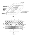
- Figure 1 is a stereogram schematically showing the ESD protection device of the present embodiment.
- Figure 2 is a sectional view schematically showing the ESD protection device of the present embodiment.
- Figure 3 is a sectional view along the line II-II shown in Figure 2 .
- the ESD protection device 100 comprises an insulating substrate 11, a pair of electrodes 21 and 22 disposed on the insulating substrate 11, a discharge inducing section 31 arranged between the electrodes 21 and 22, terminal electrodes 41 electrically connected to the electrodes 21 and 22 (see Figure 8 ) and an insulating protection layer 51 which covers the discharge inducing section 31.
- the discharge inducing section 31 has microscopic voids discontinuously dispersed therein. Also, it has a hollow structure in which one or more hollow space 31a and 31b are contained.
- the pair of electrodes 21 and 22 is arranged that their front ends portion are exposed in these hollow space 31a and 31b.
- the discharge inducing section 31 functions as an ESD protection material which discharges at a low voltage.
- the initial discharge between electrodes 21 and 22 can be ensured via the discharge inducing section 31 (hollow space 31a and 31b).
- each constituent element will be specifically described.
- the size and shape of the insulating substrate 11 are not particularly restricted as long as the insulating substrate can at least support the electrodes 21 and 22 and the discharge inducing section 31.
- the insulating substrate 11 also contains the concept of a substrate with an insulating film prepared on part or the whole surface.
- the specific example of the insulating substrate 11 can be a ceramic substrate or a single crystal substrate which uses materials with a low dielectric constant such as Al 2 O 3 , SiO 2 , MgO, AlN, Mg 2 SiO 4 or the like with a dielectric constant being 50 or less, preferably 20 or less.
- a substrate with an insulating film composed of materials with a low dielectric constant (such as Al 2 O 3 , SiO 2 , MgO, AlN, Mg 2 SiO 4 or the like with a dielectric constant being 50 or less, preferably 20 or less) can be appropriately used on the surface of the ceramic substrate or the single crystal substrate.
- a same substrate as the insulating substrate 11 can be used for the insulating protection layer 51. The repeated description will be omitted below.
- a pair of electrodes 21 and 22 is separately arranged on the insulating substrate 11.
- the pair of electrodes 21 and 22 is separately disposed with a gap distance ⁇ G in almost the middle portion of the flat plane of the insulating substrate 11.
- the gap distance ⁇ G refers to the shortest distance between electrodes 21 and 22.
- ⁇ M refers to the major axis of the hollow space 31a and ⁇ L represents the length of the discharge inducing section 31.
- the material for electrodes 21 and 22 can be at least one metal selected from the group consisting of C, Ni, Al, Fe, Cu, Ti, Cr, Au, Ag, Pd and Pt or the alloy thereof
- the material is not limited thereto.
- the electrodes 21 and 22 can be rectangular in shape when viewed from top. However, this shape is not particularly restricted.
- the gap distance ⁇ G between the electrode 21 and 22 there is no particular restriction on the gap distance ⁇ G between the electrode 21 and 22, and the gap distance can be appropriately set based on the desired discharging property.
- the ⁇ G is usually about 1 to 50 ⁇ m and is preferably 7 to 30 ⁇ m from the perspective that the initial discharge voltage is low level.
- the thickness of the electrodes 21 and 22 is not specifically restricted and generally ranges from 1 to 20 ⁇ m
- the method for forming the electrodes 21 and 22 are not particularly restricted, and well known methods can be appropriately selected. Specifically, the method can be enumerate as the coating method, transfer printing, electroplating, electroless plating, vapor plating or sputtering and the like for patterning the electrode layer with a desired thickness on the insulating laminate 11.
- the size of the electrodes 21 and 22 or gap distance ⁇ G can be processed by well-known methods such as ion milling, or etching.
- the precursor of the metal or alloy can be patterned on the substrate by the screen printing with the use of a plate for patterning the gap portion between the electrodes 21 and 22. Thereafter, a firing process is provided so that the electrodes 21 and 22 are formed.
- the electrodes 21 and 22 can be formed by simultaneously firing the object that electrodes 21 and 22 are formed on a green sheet composed of insulators by screen printing.
- the gap portion between electrodes 21 and 22 can be formed by laser processing after the precursor of metal or alloy is coated by, for example, the electrode paste.
- the discharge inducing section 31 is arranged between the electrodes 21 and 22.
- the discharge inducing section 31 is laminated on the insulating substrate 11 and electrodes 21 and 22.
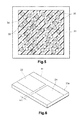
- Figure 4 is a view schematically showing the surface portion 32 of the discharge inducing at the boundary between the discharge inducing section and the hollow space in the present embodiment.
- Figure 5 is a sectional view along the line III-III shown in Figure 2 .
- the discharge inducing section 31 has a hollow structure in which hollow space 31a and 31b are contained.
- a composite with conductive inorganic material 33 uniformly or randomly dispersed in the insulating inorganic material 32 can be used as the discharge inducing section 31.
- the discharge inducing section 31 has microscopic voids 35 discontinuously dispersed therein.
- the discharge inducing section 31 of the present embodiment has a hollow structure by forming hollow space 31a and 31b and on the other hand the discharge inducing section 31 has microscopic voids 35 discontinuously dispersed therein.
- the surface portion of the discharge inducing section has dense structure.
- the surface portion 32 of the discharge inducing section contains glass at a ratio of 20 vol% or more. If the ratio of the glass is less than 20 vol%, the surface portion of the discharge inducing section is expected to not able to have a dense structure, leading to damage around the surface portion of discharge inducing section at the boundary between the discharge inducing section and the hollow space during the discharge. That is, durability is evidently deteriorated.
- the ratio of the glass in the surface portion of the discharge inducing section is preferably more than 40 vol%.
- the range of the dense structure that the surface portion of the discharge inducing section has is not particularly restricted. Considering that the melting of conductive particles generate during the discharge, the thickness of the surface portion with dense structure having glass is preferred to be about 1 to 4 ⁇ m
- the specific examples of the insulating inorganic material 34 can be metal oxides but will not limited thereto. In view of the electrical insulation or cost issues, Al 2 O 3 , SrO, CaO, BaO, TiO 2 , SiO 2 , ZnO, In 2 O 3 , NiO, CoO, SnO 2 , V 2 O 5 , CuO, MgO and ZrO 2 are preferred as the metal oxides. These materials can be used alone, or two or more of them can be used together.
- the character of the insulating inorganic material 32 is not particularly restricted. Specifically, it can be a uniform film of the insulating inorganic material 32, or it can be the particle agglomerates of the insulating material 32.
- Al 2 O 3 , SiO 2 , Mg 2 SiO 4 or the like are more preferable in view of insulation property.
- TiO 2 or ZnO is more preferable.
- An ESD protection device with a lower discharge starting voltage can be obtained by providing the insulating matrix with semiconductor related properties.
- the specific examples of the conductive inorganic material 33 can be metal, alloy, metal oxide, metal nitride, metal carbide, metal boride or the like but are not limited thereto.
- C, Ni, Al, Fe, Cu, Ti, Cr, Au, Ag, Pd and Pt or the alloy thereof are preferable.
- the surface portion 32 of discharge inducing section viewed from the hollow structure side of the discharge inducing section 31 is as shown in Figure 4 . Also, it is characterized in that it has a composite structure in which conductive inorganic material 33 is discontinuously dispersed in the insulator and the surface portion 32 of the discharge inducing section has a dense structure. With such a composite portion, the discharge is likely to occur and proceed under a low voltage. Further, as the composite portion is one with conductive inorganic material dispersed in the insulator, the insulation of the device can be maintained before or after the discharge.
- the microscopic voids 35 make the discharge inducing section 31 porous and adsorb the heat or stress generated during the discharge. In this way, the damage due to the melting or deformation of the electrodes 21 and 22 and their peripheral substances can be alleviated.
- the microscopic voids 35 refers to a gap with a size of 0.1 to 5 ⁇ m.
- the size of the microscopic voids 35 refers to the median size (D50) of a globular shape with an aspect ratio of 1 to 5, or refers to the arithmetic mean of the major axis or minor axis in other shapes. That is, the size is the mean from randomly chosen 50 points.
- the size of the microscopic voids 35 or the volume ratio of the microscopic voids 35 to the discharge inducing section 31 is not particularly restricted and can be appropriately set based on desired electrostatic adsorption property, durability against repeated discharges and prevention of short-circuiting between electrodes 21 and 22.
- the size of the microscopic voids 35 is preferably 0.1 to 2 ⁇ m, and the microscopic voids are preferably contained with a ratio of 1 to 40 vol%, and more preferably 5 to 20 vol%.
- the surface portion of the discharge inducing section at the boundary between the discharge inducing section 31 and the hollow space has a dense structure, and this structure is obtained by providing glass.
- the surface portion of the discharge inducing section preferably contains 20 vol% or more of glass components. With such a dense structure of the surface portion of the discharge inducing section, the breakage due to the stress generated during discharge can be inhibited. In this way, a device can be obtained with an excellent electrostatic adsorption property, an excellent durability against repeated discharges or a low peak voltage.
- the region of the surface portion of the discharge inducing section with a dense structure preferably has a thickness of 1 to 4 ⁇ m in a direction in depth from the hollow space to the discharge inducing section as shown in the sectional view of Figure 2 .
- the number of the hollow space in the discharge induction section 31 is not particularly limited.
- a hollow structure is employed with two hollow spaces 31a and 31b.
- the number of the hollow space is not limited and can be one or several. As the number of the hollow space increases, the frequency of discharge will decrease relative to one hollow space, resulting in further improved durability against repeated uses.
- the shape and size of each one can be the same or different.
- the shape of the hollow space 31a and 31b there is no particular restriction on the shape of the hollow space 31a and 31b. Any shape can be used such as the sphere and ellipsoid-like shape, and the hollow space can also be indefinite shape. Especially, the hollow space 31a and 31b are preferred to be a shape extending in a direction that the electrodes 21 and 22 are connected. With such hollow space 31a and 31b, the discharge generated between electrodes 21 and 22 is performed at the boundary between the hollow space and the surface portion of the discharge inducing section. Thus, the deterioration of the discharge inducing section becomes less and the durability is improved. Further, the fluctuation of the peak voltage or the discharge starting voltage can be inhibited.
- the size of the hollow space 31a,31b is not particularly restricted.
- the ⁇ M (the length of the hollow space 31a,31b in a direction that the hollow space connects the electrodes 21 and 22) preferably ranges from a half of the gap distance ⁇ G between electrodes 21 and 22 to a level less than the length ⁇ L of the discharge inducing section 31.
- the length of the hollow space 31a,31b in a direction that the hollow space connects the electrodes 21 and 22 refers to the longest length of the hollow space 31a,31b in a direction that the hollow space connects the electrodes 21 and 22.
- the length of discharge inducing section 31 refers to the longest length of the discharge inducing section 31 in a direction that the hollow space connects the electrodes 21 and 22.
- the length of the hollow space 31a,31b in a direction that the hollow space connects the electrodes 21 and 22 is 5 to 10 ⁇ m or more and this length is less than the length of the discharge inducing section 31.
- the length of the hollow space 31a,31b in a direction that the hollow space connects the electrodes 21 and 22 is set to be the gap distance ⁇ G between electrodes 21 and 22 or more so that the front ends of electrodes 21 and 22 protrude from the hollow space 31a and 31b respectively.
- the damage to the discharge inducing section due to the discharge between electrodes 21 and 22 can be inhibited.
- the deterioration of the discharge inducing section becomes less and the durability is improved.
- the fluctuation of the peak voltage or the discharge starting voltage can be inhibited.
- the thickness of the discharge inducing section 31 can be properly set and preferably ranges from the thickness of the corresponding electrode to half of the thickness of the device or less if the durability is to be improved.
- the method for forming the discharge inducing section 31 is not particularly restricted.
- the well known process for film formation as well as the lamination process can be used.
- the method described below is also suitable. Specifically, in a construction which contains a specified ratio of microscopic voids 35 with a desired size, in order to well reproduce the discharge inducing section 31 in an easy way, a mixture is coated which contains insulating inorganic materials, conductive inorganic materials and resins, wherein the resin is used to form microscopic voids 35 and will be removed during the firing process.
- the method for providing the surface portion of the discharge inducing section with a dense structure can be one in which the resin paste for forming the hollow structure contains glass and the removable materials is volatized during the firing process in order to make the surface portion of the discharge inducing section dense.
- the discharge inducing section contains glass and the glass precipitate at the boundary between the hollow space and the discharge inducing section during the firing process so that the surface portion of the discharge inducing section becomes dense.
- the method is not limited thereto.
- the preferable method for forming the discharge inducing section 31 will be described.
- a mixture is prepared to contain insulating inorganic materials, conductive inorganic materials and a removable material which is used to form the microscopic voids 35, and the mixture is coated or printed on the gap between electrodes 21 and 22.
- the mixture of the removable material which is used to form the hollow space 31a and 31b and the glass is coated or printed to a desired shape on a specified position of the mixture provided to the gap between electrodes 21 and 22.
- the mixture mentioned above can be provided via coating or printing on a specified position of the paste for forming the discharge inducing section and the paste for forming the microscopic voids.
- a firing process is provided so that the removable material is thermally degraded or volatized.
- a structure containing a specified ratio of microscopic voids 35 with a desired size can be obtained by removing the removable material during the firing process. Further, a discharge inducing section 31 can be obtained with a hollow structure in which the hollow space 31a and 31b with a desired shape are formed on a desired position and the surface portion of the discharge inducing section has a dense structure.
- the treatment conditions during the firing process are not particularly restricted. In view of the productivity and economical efficiency, the firing process is preferably performed under air atmosphere at 500 to 1200°C for 10 minutes to 5 hours.
- the removable material is no particular restriction on the removable material as long as this material will disappear (thermally degraded or volatized) during the firing process.
- Well known materials can be appropriately selected.
- the specific examples of such materials are not particularly restricted and can be resin particles or a mixed substance of a medium and resins (i.e., the resin paste).
- the representative resin particle can be a resin particle with an excellent thermal decomposability such as acrylic resins.
- the shape of the resin particle is not particularly restricted and can be any one of the hammer-like shape, the column-like shape, the sphere-like shape with an aspect ratio of 1 to 5, the ellipsoid-like shape with an aspect ratio above 5 or the like.
- the resin particle can be indeterminate form.
- the representative resin pastes can be pastes obtained by mixing resins such as the acrylic resin, ethyl cellulose and polypropylene in a well known medium, wherein said resins are thermally degraded, volatized and then disappear during the firing process.
- the particle size of the resin particles can be appropriately set in order to get the microscopic voids 35 with a desired size.
- the particle size is not particularly limited and is preferably 0.1 to 4 ⁇ m.
- the particle size of the resin particles refers to the median diameter (D50) in a sphere-like shape and refers to the arithmetic mean of the major axis and minor axis in other shapes.
- the ratio of the resin particles is not particularly restricted and can be properly set based on the ratio of microscopic voids 35 contained in the discharge inducing section 31. This ratio is preferably about 1 to 30 vol%.
- various additives such as the solvent and the binder can be added.
- the solid concentration or the viscosity of the resin paste can be properly adjusted in order to get the hollow space 31a and 31b with a desired shape or size.
- various additives can be added such as a solvent or a surfactant or a tackifier.
- the hollow space 31 a and 31b can also be prepared by a construction formed by resins or fibers, wherein this construction has a shape corresponding to the hollow space 31a and 31b with a desired shape and size and will be thermally degraded, volatized or removed during the firing process, and this construction can be used to replace the removable material or can be used together with the removable material.
- the composite i.e., the discharge inducing section 31
- the discharge inducing section 31 is composed of the structure that microscopic voids discontinuously disperse and has a hollow structure in which hollow space 31a and 31b are contained therein.
- the damage to the periphery of the electrodes and the damage to the discharge inducing section are alleviated. Accordingly, the repeating durability is significantly improved.
- the durability is further improved by making the surface portion of the discharge inducing section a dense structure.
- the discharge inducing section 31 is composed of a composite consisting of an inorganic material, so the heat resistance is further improved. Further, the properties will hardly change in accordance with the environment such as the temperature or humidity, so the reliability is elevated.
- the discharge inducing section 31 has a structure that the fused materials generated during the discharging process will hardly agglomerate on one site, so the short-circuiting between the electrodes 21 and 22 can be effectively prevented.
- an ESD protection device 100 with good performance will be obtained which has a low electrostatic capacitance, an excellent electrostatic adsorption property.
- the discharge durability is improved, the peak voltage is suppressed to a low level, and the short-circuiting between electrodes after discharges is inhibited, and an excellent heat resistance and an excellent climate resistance can be obtained.
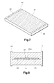
- a green sheet obtained by making the materials consisting of the main component Al 2 O 3 and the glass component into a sheet was used as an insulating substrate 11 shown in Figure 6 .
- An Ag paste was printed with a thickness of 20 ⁇ m on one insulating surface 11 a by screen printing so as to pattern and form a pair of oppositely disposed strip-like electrodes 21 and 22.
- the pair of printed electrodes the length of each of electrodes 21 and 22 was both 0.5 mm and the width was 0.4 mm, and the gap distance ⁇ G between two electrodes 21 and 22 was 40 ⁇ m.
- a discharge inducing section 31 was formed on the insulating substrate 11 and the electrodes 21 and 22 in the following orders.
- glass particles with SiO 2 as the main component (which are used as the insulating inorganic material 34) (trade name: ME13, prepared by Nihon Yamamura Glass Co., Ltd)being 10 vol%, Al 2 O 3 with an average particle size of 1 ⁇ m (which is used as the insulating inorganic material 34) (trade name: AM-27, prepared by Sumitomo Chemical Co., Ltd) being 60 vol%, Ag particles with an average particle size of 1 ⁇ m (which are used as the conductive inorganic material 33) (trade name: SPQ05S, prepared by Mitsui Kinzoku Co., Ltd) being 30 vol% and spherical acrylic resin particles with an average particle size of 1 ⁇ m (which are used to form microscopic voids 35) being 30 vol% (trade name: MX-150, prepared by Soken Chemical & Engineering Co., Ltd.) were measured and mixed to obtain a mixture.
- MX-150 prepared by Soken Chemical & Engineering Co., Ltd.
- a lacquer with a solid concentration of 8 mass% was prepared by mixing the ethyl cellulose-based resin as a binder and the terpineol as a solvent. Next, the lacquer was added into the obtained mixture mentioned above. Then, they were mixed to prepare a paste mixture for the formation of discharge inducing section.
- the acrylic resin was mixed into the butyl carbitol, and a resin paste with a solid concentration of 40 mass% was formed for the preparation of hollow space 31a and 31b.
- the glass particles mentioned above were mixed in the resin paste, and a paste-like mixture mixed with the glass ,which was for the formation of the hollow space, was prepared.
- the obtained paste-like mixture (which was for the formation of discharge inducing section) was coated in a small amount by screen printing to cover the insulating surface 11 a of the insulating substrate 11 between electrodes 21 and 22.
- the paste-like mixture for the formation of hollow space was screen printed on two sites in an ellipsoid-like shape. After that, a screen printing was performed to cover the paste-like mixture for the formation of the discharge inducing section and the coated ellipsoidal paste-like mixture for the formation of the hollow space so that a precursor of the discharge inducing section 31 similar to that shown in Figure 1 was formed.
- a laminate was prepared by a hot pressing. Thereafter, the obtained laminate was cut into individual pieces with a specified size. The individual pieces of laminates were subjected to the thermal treatment at 200 °C for 1 hour (the process of removing the binder). Then, the temperature was raised with a rate of 10°C/min and the individual pieces of laminates were kept under air atmosphere at 950°C for 30 minutes. With such a firing treatment, the acrylic resins, ethyl cellulose based resins and the solvent were removed from the precursor of the discharge inducing section 31. As a result, a construction was formed with microscopic voids 35 discontinuously dispersed therein.
- a discharge inducing section 31 was prepared in which a hollow structure was formed (which has hollow space 31a and 31b formed therein) and the surface portion of the discharge inducing section has a dense structure. Further, the gap distance ⁇ G between the pair of fired electrodes 21 and 22 was about 30 ⁇ m and the length ⁇ M of each of the hollow space 31a and 31b was 40 ⁇ m in a direction that the electrodes 21 and 22 are connected.
- a terminal electrode 41 with Ag as the main component was formed by connecting to the outside ends of the electrodes 21 and 22. In this way, the ESD protection device 100 of Example 1 was obtained.
- a discharge inducing section 31 (which was formed by a construction with microscopic voids 35 discontinuously dispersed and had a hollow structure in which one hollow space 31a was contained) was prepared in the same way as in Example 1 except that the screen printing was applied to only one site in an ellipsoid-like shape during the screen printing process of the paste-like mixture for the formation of the hollow space. In this way, the ESD protection device 100 of Example 2 was obtained.
- a discharge inducing section without a hollow structure (which was formed by a construction with microscopic voids 35 discontinuously dispersed) was prepared in the same way as in Example 1 except that, while the paste-like mixture for formation of hollow space is screen printed, the paste-like mixture for the formation of discharge inducing section was used instead of the paste-like mixture for formation of hollow space. In this way, the ESD protection device of Comparative Example 1 was obtained.
- a discharge inducing section without a hollow space (which was formed by a construction with microscopic voids 35 discontinuously dispersed) was prepared in the same way as in Example 1 except that spherical acrylic resin particles with an average particle size of 2.0 ⁇ m (trade name: MX-200, prepared by Soken Chemical & Engineering Co., Ltd.) was used to form microscopic voids 35 instead of spherical acrylic resin particles with an average particle size of 1.0 ⁇ m (trade name: MX-150, prepared by Soken Chemical & Engineering Co., Ltd.). In this way, the ESD protection device of Comparative Example 2 was obtained.
- a discharge inducing section 31 (which was formed by a construction with microscopic voids 35 discontinuously dispersed and had a hollow structure in which hollow space 31a and 31b were contained) was prepared in the same way as in Example 1 except that spherical acrylic resin particles with an average particle size of 1.0 ⁇ m (trade name: MX-150, prepared by Soken Chemical & Engineering Co., Ltd.) for formation of microscopic voids 35 were used and the discharge inducing section is changed to 10 vol% of glass particles, 50 vol% of Al 2 O 3 , 30 vol% of Ag particles and 10 vol% of acrylic resin particles. In this way, the ESD protection device 100 of Example 3 was obtained.
- a discharge inducing section 31 (which was formed by a porous construction with microscopic voids 35 discontinuously dispersed and had a hollow structure in which one hollow space 31a was contained) was prepared in the same way as in Example 2 except that 10 vol% of glass particles, 50 vol% of Al 2 O 3 and 30 vol% of Ag particles were used to form the discharge inducing section and 10 vol% of acrylic resin particles MX-150 was replaced by 10 vol% of spherical acrylic resin particles with an average particle size of 2.0 ⁇ m (trade name: MX-300, prepared by Soken Chemical & Engineering Co., Ltd.). In this way, the ESD protection device 100 of Example 4 was obtained.
- a discharge inducing section 31 (which was formed by a construction with microscopic voids 35 discontinuously dispersed and had a hollow structure in which hollow space 31a and 31b were contained) was prepared in the same way as in Example 3 except that 10 vol% of glass particles, 50 vol% of Al 2 O 3 and 30 vol% of Ag particles were used to form the discharge inducing section, and 10 vol% of acrylic resin particles MX-150 were used and two hollow space were contained. In this way, the ESD protection device 100 of Example 5 was obtained.
- a discharge inducing section without a hollow structure (which was formed by a construction with microscopic voids 35 discontinuously dispersed) was prepared in the same way as in Comparative Example 1 except that 10 vol% of glass particles, 50 vol% of Al 2 O 3 and 30 vol% of Ag particles were used to form the discharge inducing section and 10 vol% of acrylic resin particles MX-150 were used. In this way, the ESD protection device 100 of Comparative Example 3 was obtained.
- a discharge inducing section without a hollow structure (which was formed by a construction with microscopic voids 35 discontinuously dispersed) was prepared in the same way as in Comparative Example 3 except that 10 vol% of acrylic resin particles MX-150 were replaced with 10 vol% of spherical acrylic resin particles with an average particle size of 3.0 ⁇ m (trade name: MX-300, prepared by Soken Chemical & Engineering Co., Ltd.). In this way, the ESD protection device of Comparative Example 4 was obtained.
- a discharge inducing section 31 (which was formed by a construction with microscopic voids 35 discontinuously dispersed and had a hollow structure in which one hollow space 31a was contained and the surface portion of discharge inducing section does not have a dense structure) was prepared in the same way as in Example 3 except that the process of adding glass is omitted during the preparation of paste-like mixture for formation of hollow space. In this way, the ESD protection device 100 of Comparative Example 5 was obtained.
- a discharge inducing section without microscopic voids 35 or a hollow space was prepared in the same way as in Comparative Example 1 except that the acrylic resin particles were not added and the ratios for each component were changed to 15 vol% of glass particles, 55 vol% of Al 2 O 3 and 30 vol% of Ag particles. In this way, the ESD protection device 100 of Comparative Example 5 was obtained.
- the section of the discharge inducing section 31 (the section where hollow space 31a and 31b were not formed) was polished. These sections were observed by SEM and photos were taken. In the photos, the images of the microscopic voids were processed and the sum of the areas of these microscopic voids was calculated. Then, the ratio of the microscopic voids was obtained by dividing the sum by the total areas.
- the electrostatic discharge test was performed for the ESD protection devices 100 of Examples 1 to 5 and Comparative Examples 1 to 6 by using the circuit shown in Figure 9 .
- the test results were shown in Table 1 and Table 2.
- the electrostatic discharge test was carried out following the human body model (discharge resistance was 330 ⁇ , discharge capacitance was 150 pF, applied voltage was 8.0 kV, contact discharge) based on the IEC61000-4-2 electrostatic discharge immunity test and the noise test. Specifically, as shown in the circuit for electrostatic test in Figure 9 , one terminal electrode of the ESD protection device as the evaluation subject was connected to the ground while the other terminal electrode was connected to the electrostatic pulse applying portion so that the electrostatic pulses were applied when the electrostatic pulse applying portion contacted the discharge gun.
- the applied electrostatic pulse provides a voltage above the discharge starting voltage.
- the electrostatic discharge test was performed while the discharge starting voltage was firstly set as 0.4 kV and then was increased by 0.2 kV at each round. The observed waveforms of the electrostatic adsorption were recorded, and the voltage at which the electrostatic adsorption effect was revealed was used as the discharge starting voltage.
- the electrostatic capacitance was the electrostatic capacitance (pF) at 1 MHz.
- the short-circuiting rate 100 samples for each were prepared, and the electrostatic discharge test was repeated for 100 times at 8.0 kV. The number of occurrence of short-circuiting between electrodes was counted and was shown by its ratio (%). With respect to the durability, 100 items were prepared for each sample, and the electrostatic discharge test was repeated for 1000 times at 8.0 kV.
- the peak voltage at the 1000th discharge was measured for each sample.
- the number of samples with the peak voltage being 400V or less was counted and was shown by its ratio (%). Further, the same discharge test was performed for the peak voltage. Specifically, the 1000th peak voltage was measured for each sample and the mean was calculated. The lower the peak voltage was, the better the electrostatic adsorption effect was, which was good for an ESD protection device.
- the ESD protection devices of Examples 1 to 5 all had a discharge starting voltage lower than 2 kV and an electrostatic capacitance lower than 0.2 pF. Thus, they had good performance and were applicable to high-speed transmission system. Further, the occurrence of short-circuiting between electrodes was significantly inhibited in the ESD protection devices from Examples 1 to 5. Also, based on the results of the discharge test, for the ESD protection devices of Examples 1 to 5, the durability against repeated discharge was excellent and the peak voltage was suppressed to a low level.
- the present invention is not limited to the embodiments and examples mentioned above, and various modifications may be made without changing the spirit.
- the number, shape, size and layout of the hollow space 31a and 31b can be changed.
- two hollow space 31 a and 31b can be made in a prism-like shape.
- three hollow space 31a, 31b and 31c can be provided, as shown in Figure 11 .
- one electrode 21 can be disposed on the insulting substrate 11 and the other electrode 22 can be arranged on the insulating protection layer 51 so that the pair of electrodes 21 and 22 are separately and oppositely disposed.
- the ESD protection device of the present invention has a low electrostatic capacitance and an excellent durability against repeated discharge.
- the short-circuiting between electrodes can be inhibited and the peak voltage can be inhibited to a low level.
- the ESD protection device of the present invention has an excellent heat resistance and an excellent climate resistance. Also, the productivity and economical efficiency can be elevated. Thus, it can be widely and effectively used in electric or electrical devices having ESD protection devices and various machines, equipments and systems containing these electric or electrical devices.
Landscapes
- Thermistors And Varistors (AREA)
- Vessels And Coating Films For Discharge Lamps (AREA)
- Physical Or Chemical Processes And Apparatus (AREA)
Abstract
Description
- The present invention relates to an ElectroStatic Discharge(ESD) protection device, especially an ESD protection device useful in the application of a high-speed transmission system or the integration with common mode filters.
- Recently, the downsizing and performance improvement of the electric devices are under rapid development. Also, the improvement of the frequency on the transmission speed and the lowering of driving voltage are remarkable, as seen in the high-speed transmission systems such as USB 2.0, S-ATA2, HDMI or the like. On the contrary, with the downsizing or the lowering of driving voltage of the electric devices, the breakdown voltage of the electric components which are used in the electric devices is decreased. In this respect, the protection of the electric components from overvoltage becomes an important technical subject, for example, protecting the electric components against the electrostatic pulses derived from the contact between the human body and the terminal of an electric device.
- In the past, in order to protect electric components from such electric pulse, a method of providing a varistor between the ground and a line to be subjected to static electricity has generally been used. As the signal frequency of the signal line is being rapidly increased in recent years, the signal quality deteriorates when the electrostatic capacitance of the ESD protection device is large. Thus, when the transmission speed is up to several hundreds of Mbps or more, a protection device with a low electrostatic capacitance (1 pF or less) is needed. In addition, an ESD protection device with a large electrostatic capacitance cannot be used in an antenna circuit and an RF module.
- It has been suggested that an ESD protection device with a discharge inducing section filled between two separately and oppositely arranged electrodes can be used as an ESD device with a low electrostatic capacitance. This device is arranged between the ground and a line to be subjected to static electricity in the same way of a laminated varistor. If a much too high voltage is applied, discharge will happen between the oppositely arranged electrodes of the ESD protection device and then the static electricity will be led to the ground side. Such ESD protection device of gap type possesses properties such as a high insulation resistance, a low electrostatic capacitance and a good responsiveness.
- In another respect, as an important property of the ESD protection device, the property of electrostatic adsorption is also presented as a subject of the present invention. If the discharging process occurs under a low voltage, it is necessary to restrain the peak voltage during the discharging process. If the peak voltage cannot be suppressed to a certain level, a device becoming the protection object may be destroyed. In this respect, it is necessary to restrain the peak voltage to a low level. Further, the durability issue related to repeated operations is presented here. The peak voltage should still be restrained after a plurality of discharging processes. In order to solve these technical problems, a circuit protection device, in which cavities are disposed around the oppositely arranged electrodes, is disclosed.
-
- Patent Document 1:
JP4247581 - Patent Document 2:
JP2008-244348 - Patent Document 3:
WO2010-061519 - Patent Document 4:
WO2010-061550 - However, although the ESD protection device disclosed in Patent Document 1 can adsorb the heat or stress generated in the discharging process by the hole portion which is disposed above the two opposite electrodes, the discharge inducing section (the ESD protection material) is only formed below the two opposite electrodes so that stable discharges may not happen.
- In the technology disclosed in Patent Document 2, an ESD protection material is provided by filling composite particles between two oppositely disposed electrodes. In the composite particles, the conductive particles have their surfaces covered by inorganic glasses. Thus, it is not able to obtain an ESD protection device with high performance which is applicable to the high-speed transmission systems. In addition, the heat or stress derived from the discharge cannot be completely absorbed by small holes formed among composite particles. Thus, breakage occurs around the electrodes and fused materials are generated between electrodes. In this way, short-circuiting will happen between electrodes due to the agglomeration of fused materials.
- The ESD protection device disclosed in Patent Document 3 has such a structure that the discharge inducing section are provided on the upper and lower surfaces of the oppositely disposed electrodes and a hole is formed in the middle. In such a structure, as the hole is quite long in width, stable discharges may not happen. When the conductive substances on the surfaces of the discharge inducing section are melted, the short-circuiting between electrodes may occur due to the agglomeration of fused materials.
- In the ESD protection device disclosed in Patent Document 4, conductive powder form auxiliary electrode are dispersed between the discharge electrodes which exposed to the inside of the hole portion. This ESD protection device can adsorb the heat or stress derived by discharge. However, the accessorial electrode materials may be destroyed during the discharge.
- In view of the problems mentioned above, the present invention aims to provide an ESD protection device with a low electrostatic capacitance, an excellent electrostatic adsorption property and an excellent durability. Also, such an ESD protection device can inhibit the damage from the short-circuiting and heat resistance and climate resistance as well as excellent productivity and economical efficiency.
- In order to solve the technical problems mentioned above, the inventors provide a discharge inducing section around two oppositely disposed electrodes. This discharge inducing section consists of a conductive inorganic material and an insulating inorganic material and has a structure in which microscopic voids are dispersed. In addition, the discharge inducing section has a hollow space inside, wherein the hollow space is in a direction that two oppositely disposed electrodes are connected. Thus, an ESD protection device can be provided with a decreased short-circuiting rate or a reduced peak voltage because it has a low electrostatic capacitance, an excellent durability and can inhibit the damage from short-circuiting.
- The hollow space is formed in a direction that the two oppositely disposed electrodes are connected, and the length of the hollow space necessarily ranges from a level that is half of the interval between two opposite electrodes to a level that is less than the length of the discharge inducing section. In addition, the width of the hollow space should be less than that of the discharge inducing section. In other words, the hollow space has to be formed inside the discharge inducing section. On the plane of the discharge inducing section where the hollow space is formed, a composite structure has to be employed in which conductive substances are discontinuously dispersed in the insulating material. With such a structure, the discharge occurs at the boundary between the discharge inducing section and the hollow space. Further, when a static voltage is applied, the plane formed with a hollow structure may be broken. However, in the condition that such breakage happened, the plane has a dense structure so that the drop off of the surface portion can be inhibited. In this way, after multiple discharge, the electrostatic adsorption property can be maintained. In addition, when excessive static voltage is applied, the discharge function can be maintained even if part of the surface portion of the plane formed with a hollow structure is melted during the discharge. This is because the inner side of this plane is exposed.
- The discharge inducing section consists of a conductive inorganic material and an insulating inorganic material. In the discharge inducing section, microscopic voids are necessarily formed. The microscopic voids may adsorb the impact during the discharging process and can inhibit damage derived from short-circuiting by absorbing fused materials in the voids in the condition that the conductive particles are melted during the discharge. Such an effect can be achieved if the size of the gap is set to be 0.1 to 2 times of the average particle size of the conductive particles.
- The distance between two oppositely disposed electrodes can be appropriately set as long as the desired discharging property is considered. Such a distance is usually about 1 to 50 µm This distance is preferably about 7 to 30 µm, in terms of decreasing peak voltage.
- After the measurements of performance of the ESD protection device mentioned above, the inventors confirmed that this ESD protection device has excellent electrostatic adsorption property, durability and peak voltage compared to the conventional ones. The functions owned by an ESD protection device can be still maintain after multiple discharge.
- In the past, in such a gap type ESD protection device, discharge usually occurs in a place between the opposite electrodes where discharge occurs easily. Thus, once the discharge occurs, the next discharge will occur in the other. Thus, the discharging property tends to fluctuate. In anther respect, the place for discharging will be focused by providing a structure that a hollow space is formed in the discharge inducing section along the direction that the opposite electrodes are connected. Accordingly, the fluctuation of the discharging property will be decreased.
- In conventional devices, if much excessive static voltage is applied and the discharge inducing section is subject to arc discharge, conductive fused materials are formed between opposite electrodes which occur short-circuiting between the opposite electrodes. In another respect, microscopic voids are formed in the discharge inducing section itself. Even if the discharge inducing section is melted due to the discharging process, the fused materials can run into the microscopic voids so that the short-circuiting between opposite electrodes due to the fused materials can be inhibited. In other words, when the discharge happens at the boundary between the discharge inducing section and the hollow space and fused materials are formed accordingly, let the fused materials loose into the microscopic voids in the inner side of the discharge induction section so that the short-circuiting at the discharging place can be inhibited. Further, as the surface portion of the discharge inducing section at the boundary between the discharge inducing section and the hollow space has a dense structure, damages can be prevented which may be caused by the dropping off of the discharging place due to the impact during the discharge. In this respect, especially the peak voltage can be suppressed to a low level, and the functions owned by an ESD protection device can be maintained after multiple discharge. A dense structure is used for the surface portion of the discharge inducing section while the discharge inducing section is porous with microscopic voids. Here, in order to provide the surface portion of the discharge inducing section with a dense structure, glass is used so that the region confined by the surface part has less voids. The ratio of the glass in the surface portion of the discharge inducing section should be 20 vol% or more so as to form such a structure.
- The ESD protection device of the present invention possesses a substrate with a insulting surface, electrodes separately and oppositely disposed on the insulating surface with each other and a discharge inducing section which at least arranged between two electrodes, wherein the discharge inducing section has a composite structure that conductive particles, insulating particles and microscopic voids are dispersed therein. The discharge inducing section has a hollow structure which has a hollow space in a direction that the opposite electrodes are connected. An ESD protection device which has an excellent electrostatic adsorption property and an excellent durability and can inhibit the damage derived from short-circuiting or the peak voltage can be provided by forming a composite structure with conductive substances of the surface portion of the discharge inducing section discontinuously dispersed in the insulating materials and providing the surface portion of the discharge inducing section (at the boundary between the discharge inducing section and the hollow space) with a dense structure.
- The other embodiments of the present invention involve composite electric components integrated with the ESD protection device of the present invention, i.e., the composite electric components have an inductance element in a magnetic substrate, which is integrated with the ESD protection device. The inductance element has a conductor pattern in the magnetic substrate. The ESD protection device has a structure having separately and oppositely disposed electrodes in the insulating substrate integrated with the magnetic substrate, and a functional layer with at least part of which disposed between the electrodes.
- Based on such a structure, the ESD protection device of the present invention has a low electrostatic capacitance, a low rate of short-circuiting and an excellent durability. Also, the ESD protection device can inhibit the damage derived from short-circuiting or the peak voltage.
-
-
Figure 1 is a stereogram schematically showing theESD protection device 100. -
Figure 2 is a sectional view schematically showing theESD protection device 100. -
Figure 3 is a sectional view along the line II-II shown inFigure 2 . -
Figure 4 is a stereogram schematically showing thesurface portion 32 of the discharge inducing section. -
Figure 5 is a sectional view along the line III-III shown inFigure 2 . -
Figure 6 is a stereogram schematically showing the preparation process of theESD protection device 100. -
Figure 7 is a stereogram schematically showing the preparation process of theESD protection device 100. -
Figure 8 is a stereogram schematically showing the preparation process of theESD protection device 100. -
Figure 9 shows the circuit diagram in the ESD discharge test. -
Figure 10 is a schematic sectional view showing a first modification. -
Figure 11 is a schematic sectional view showing a second modification. -
Figure 12 is a schematic sectional view showing a third modification. - Hereinafter, the embodiments of the present invention will be described. The same reference number is used for the same element, and the repeated descriptions will be omitted. The positional relationship is based on the drawings unless otherwise specified. In addition, the dimensional proportions are not limited to those shown in the drawings. Although the following embodiments are used to describe the present invention, the present invention is not limited to these embodiments.
-
Figure 1 is a stereogram schematically showing the ESD protection device of the present embodiment.Figure 2 is a sectional view schematically showing the ESD protection device of the present embodiment.Figure 3 is a sectional view along the line II-II shown inFigure 2 . - The
ESD protection device 100 comprises an insulatingsubstrate 11, a pair ofelectrodes substrate 11, adischarge inducing section 31 arranged between theelectrodes terminal electrodes 41 electrically connected to theelectrodes 21 and 22 (seeFigure 8 ) and an insulatingprotection layer 51 which covers thedischarge inducing section 31. Thedischarge inducing section 31 has microscopic voids discontinuously dispersed therein. Also, it has a hollow structure in which one or morehollow space electrodes hollow space ESD protection device 100, thedischarge inducing section 31 functions as an ESD protection material which discharges at a low voltage. When an overvoltage such as static electricity is applied, the initial discharge betweenelectrodes hollow space - The size and shape of the insulating
substrate 11 are not particularly restricted as long as the insulating substrate can at least support theelectrodes discharge inducing section 31. Here, besides the substrate composed of an insulating material, the insulatingsubstrate 11 also contains the concept of a substrate with an insulating film prepared on part or the whole surface. - The specific example of the insulating
substrate 11 can be a ceramic substrate or a single crystal substrate which uses materials with a low dielectric constant such as Al2O3, SiO2, MgO, AlN, Mg2SiO4 or the like with a dielectric constant being 50 or less, preferably 20 or less. In addition, a substrate with an insulating film composed of materials with a low dielectric constant (such as Al2O3, SiO2, MgO, AlN, Mg2SiO4 or the like with a dielectric constant being 50 or less, preferably 20 or less) can be appropriately used on the surface of the ceramic substrate or the single crystal substrate. Then, for the insulatingprotection layer 51, a same substrate as the insulatingsubstrate 11 can be used. The repeated description will be omitted below. - On the insulating
substrate 11, a pair ofelectrodes electrodes substrate 11. Here, the gap distance ΔG refers to the shortest distance betweenelectrodes hollow space 31a and ΔL represents the length of thedischarge inducing section 31. - As for the material for
electrodes electrodes - There is no particular restriction on the gap distance ΔG between the
electrode electrodes - The method for forming the
electrodes laminate 11. In addition, the size of theelectrodes electrodes electrodes electrodes electrodes electrodes - The
discharge inducing section 31 is arranged between theelectrodes discharge inducing section 31 is laminated on the insulatingsubstrate 11 andelectrodes discharge inducing section 31 as long as the discharging process occurs between theelectrodes discharge inducing section 31 when an overvoltage is applied. -
Figure 4 is a view schematically showing thesurface portion 32 of the discharge inducing at the boundary between the discharge inducing section and the hollow space in the present embodiment.Figure 5 is a sectional view along the line III-III shown inFigure 2 . Thedischarge inducing section 31 has a hollow structure in which hollowspace inorganic material 33 uniformly or randomly dispersed in the insulatinginorganic material 32 can be used as thedischarge inducing section 31. As shown inFigure 5 , thedischarge inducing section 31 hasmicroscopic voids 35 discontinuously dispersed therein. In other words, thedischarge inducing section 31 of the present embodiment has a hollow structure by forminghollow space discharge inducing section 31 hasmicroscopic voids 35 discontinuously dispersed therein. In addition, the surface portion of the discharge inducing section has dense structure. - The
surface portion 32 of the discharge inducing section contains glass at a ratio of 20 vol% or more. If the ratio of the glass is less than 20 vol%, the surface portion of the discharge inducing section is expected to not able to have a dense structure, leading to damage around the surface portion of discharge inducing section at the boundary between the discharge inducing section and the hollow space during the discharge. That is, durability is evidently deteriorated. Thus, in order to form a dense structure, the ratio of the glass in the surface portion of the discharge inducing section is preferably more than 40 vol%. The range of the dense structure that the surface portion of the discharge inducing section has is not particularly restricted. Considering that the melting of conductive particles generate during the discharge, the thickness of the surface portion with dense structure having glass is preferred to be about 1 to 4 µm - The specific examples of the insulating
inorganic material 34 can be metal oxides but will not limited thereto. In view of the electrical insulation or cost issues, Al2O3, SrO, CaO, BaO, TiO2, SiO2, ZnO, In2O3, NiO, CoO, SnO2, V2O5, CuO, MgO and ZrO2 are preferred as the metal oxides. These materials can be used alone, or two or more of them can be used together. The character of the insulatinginorganic material 32 is not particularly restricted. Specifically, it can be a uniform film of the insulatinginorganic material 32, or it can be the particle agglomerates of the insulatingmaterial 32. Among these materials, Al2O3, SiO2, Mg2SiO4 or the like are more preferable in view of insulation property. In order to provide the insulating matrix with semiconductor related properties, TiO2 or ZnO is more preferable. An ESD protection device with a lower discharge starting voltage can be obtained by providing the insulating matrix with semiconductor related properties. - The specific examples of the conductive
inorganic material 33 can be metal, alloy, metal oxide, metal nitride, metal carbide, metal boride or the like but are not limited thereto. In view of the electrical conductivity, C, Ni, Al, Fe, Cu, Ti, Cr, Au, Ag, Pd and Pt or the alloy thereof are preferable. - The
surface portion 32 of discharge inducing section viewed from the hollow structure side of thedischarge inducing section 31 is as shown inFigure 4 . Also, it is characterized in that it has a composite structure in which conductiveinorganic material 33 is discontinuously dispersed in the insulator and thesurface portion 32 of the discharge inducing section has a dense structure. With such a composite portion, the discharge is likely to occur and proceed under a low voltage. Further, as the composite portion is one with conductive inorganic material dispersed in the insulator, the insulation of the device can be maintained before or after the discharge. - The
microscopic voids 35 make thedischarge inducing section 31 porous and adsorb the heat or stress generated during the discharge. In this way, the damage due to the melting or deformation of theelectrodes microscopic voids 35 refers to a gap with a size of 0.1 to 5 µm. Further, in the present specification, the size of themicroscopic voids 35 refers to the median size (D50) of a globular shape with an aspect ratio of 1 to 5, or refers to the arithmetic mean of the major axis or minor axis in other shapes. That is, the size is the mean from randomly chosen 50 points. The size of themicroscopic voids 35 or the volume ratio of themicroscopic voids 35 to thedischarge inducing section 31 is not particularly restricted and can be appropriately set based on desired electrostatic adsorption property, durability against repeated discharges and prevention of short-circuiting betweenelectrodes microscopic voids 35 is preferably 0.1 to 2 µm, and the microscopic voids are preferably contained with a ratio of 1 to 40 vol%, and more preferably 5 to 20 vol%. - The surface portion of the discharge inducing section at the boundary between the
discharge inducing section 31 and the hollow space has a dense structure, and this structure is obtained by providing glass. The surface portion of the discharge inducing section preferably contains 20 vol% or more of glass components. With such a dense structure of the surface portion of the discharge inducing section, the breakage due to the stress generated during discharge can be inhibited. In this way, a device can be obtained with an excellent electrostatic adsorption property, an excellent durability against repeated discharges or a low peak voltage. Further, the region of the surface portion of the discharge inducing section with a dense structure preferably has a thickness of 1 to 4 µm in a direction in depth from the hollow space to the discharge inducing section as shown in the sectional view ofFigure 2 . - The number of the hollow space in the
discharge induction section 31 is not particularly limited. In the present embodiment, a hollow structure is employed with twohollow spaces - Also, there is no particular restriction on the shape of the
hollow space hollow space electrodes hollow space electrodes - In another respect, the size of the
hollow space hollow space electrodes 21 and 22) preferably ranges from a half of the gap distance ΔG betweenelectrodes discharge inducing section 31. In addition, the length of thehollow space electrodes hollow space electrodes discharge inducing section 31 refers to the longest length of thedischarge inducing section 31 in a direction that the hollow space connects theelectrodes ESD protection device 100, the length of thehollow space electrodes discharge inducing section 31. As shown inFigure 2 andFigure 3 , the length of thehollow space electrodes electrodes electrodes hollow space electrodes - There is no particular restriction on the thickness of the
discharge inducing section 31. That is, the thickness can be properly set and preferably ranges from the thickness of the corresponding electrode to half of the thickness of the device or less if the durability is to be improved. - The method for forming the
discharge inducing section 31 is not particularly restricted. For example, the well known process for film formation as well as the lamination process can be used. The method described below is also suitable. Specifically, in a construction which contains a specified ratio ofmicroscopic voids 35 with a desired size, in order to well reproduce thedischarge inducing section 31 in an easy way, a mixture is coated which contains insulating inorganic materials, conductive inorganic materials and resins, wherein the resin is used to formmicroscopic voids 35 and will be removed during the firing process. Thereafter, the resultant product obtained by mixing the removable material, which is used to form thehollow space microscopic voids 35 is formed and a hollow structure is defined and formed in which the surface portion of the discharge inducing section at the boundary with the hollow space is provided with a dense structure. The method for providing the surface portion of the discharge inducing section with a dense structure can be one in which the resin paste for forming the hollow structure contains glass and the removable materials is volatized during the firing process in order to make the surface portion of the discharge inducing section dense. Alternatively, another method can be used that the discharge inducing section contains glass and the glass precipitate at the boundary between the hollow space and the discharge inducing section during the firing process so that the surface portion of the discharge inducing section becomes dense. However, the method is not limited thereto. Hereinafter, the preferable method for forming thedischarge inducing section 31 will be described. - In this method, a mixture is prepared to contain insulating inorganic materials, conductive inorganic materials and a removable material which is used to form the
microscopic voids 35, and the mixture is coated or printed on the gap betweenelectrodes hollow space electrodes microscopic voids 35 with a desired size can be obtained by removing the removable material during the firing process. Further, adischarge inducing section 31 can be obtained with a hollow structure in which thehollow space - Furthermore, these is no particular restriction on the removable material as long as this material will disappear (thermally degraded or volatized) during the firing process. Well known materials can be appropriately selected. The specific examples of such materials are not particularly restricted and can be resin particles or a mixed substance of a medium and resins (i.e., the resin paste). The representative resin particle can be a resin particle with an excellent thermal decomposability such as acrylic resins. Further, the shape of the resin particle is not particularly restricted and can be any one of the hammer-like shape, the column-like shape, the sphere-like shape with an aspect ratio of 1 to 5, the ellipsoid-like shape with an aspect ratio above 5 or the like. Also, the resin particle can be indeterminate form. Further, the representative resin pastes can be pastes obtained by mixing resins such as the acrylic resin, ethyl cellulose and polypropylene in a well known medium, wherein said resins are thermally degraded, volatized and then disappear during the firing process. Here, when the
microscopic voids 35 are formed by resin particles, the particle size of the resin particles can be appropriately set in order to get themicroscopic voids 35 with a desired size. The particle size is not particularly limited and is preferably 0.1 to 4 µm. Furthermore, in the present specification, the particle size of the resin particles refers to the median diameter (D50) in a sphere-like shape and refers to the arithmetic mean of the major axis and minor axis in other shapes. In this respect, the ratio of the resin particles is not particularly restricted and can be properly set based on the ratio ofmicroscopic voids 35 contained in thedischarge inducing section 31. This ratio is preferably about 1 to 30 vol%. During the preparation of the mixture, various additives such as the solvent and the binder can be added. When resin paste is used to form thehollow space hollow space hollow space hollow space - In the
ESD protection device 100 of the present embodiment, the composite (i.e., the discharge inducing section 31) with the conductiveinorganic material 33 discontinuously dispersed in the insulating inorganic material functions as an ESD protection material with a large insulation resistance, a low electrostatic capacitance and an excellent discharging property. Then, thedischarge inducing section 31 is composed of the structure that microscopic voids discontinuously disperse and has a hollow structure in which hollowspace discharge inducing section 31 is composed of a composite consisting of an inorganic material, so the heat resistance is further improved. Further, the properties will hardly change in accordance with the environment such as the temperature or humidity, so the reliability is elevated. Thedischarge inducing section 31 has a structure that the fused materials generated during the discharging process will hardly agglomerate on one site, so the short-circuiting between theelectrodes ESD protection device 100 with good performance will be obtained which has a low electrostatic capacitance, an excellent electrostatic adsorption property. Also, in such an ESD protection device, the discharge durability is improved, the peak voltage is suppressed to a low level, and the short-circuiting between electrodes after discharges is inhibited, and an excellent heat resistance and an excellent climate resistance can be obtained. - Hereinafter, the present invention will be specifically described based on Examples. However, the present invention will not be limited thereto.
- First of all, a green sheet obtained by making the materials consisting of the main component Al2O3 and the glass component into a sheet was used as an insulating
substrate 11 shown inFigure 6 . An Ag paste was printed with a thickness of 20 µm on one insulatingsurface 11 a by screen printing so as to pattern and form a pair of oppositely disposed strip-like electrodes electrodes electrodes - As shown in
Figure 7 , adischarge inducing section 31 was formed on the insulatingsubstrate 11 and theelectrodes - First of all, glass particles with SiO2 as the main component (which are used as the insulating inorganic material 34) (trade name: ME13, prepared by Nihon Yamamura Glass Co., Ltd)being 10 vol%, Al2O3 with an average particle size of 1 µm (which is used as the insulating inorganic material 34) (trade name: AM-27, prepared by Sumitomo Chemical Co., Ltd) being 60 vol%, Ag particles with an average particle size of 1 µm (which are used as the conductive inorganic material 33) (trade name: SPQ05S, prepared by Mitsui Kinzoku Co., Ltd) being 30 vol% and spherical acrylic resin particles with an average particle size of 1 µm (which are used to form microscopic voids 35) being 30 vol% (trade name: MX-150, prepared by Soken Chemical & Engineering Co., Ltd.) were measured and mixed to obtain a mixture. Besides, a lacquer with a solid concentration of 8 mass% was prepared by mixing the ethyl cellulose-based resin as a binder and the terpineol as a solvent. Next, the lacquer was added into the obtained mixture mentioned above. Then, they were mixed to prepare a paste mixture for the formation of discharge inducing section.
- Thereafter, the acrylic resin was mixed into the butyl carbitol, and a resin paste with a solid concentration of 40 mass% was formed for the preparation of
hollow space - Then, the obtained paste-like mixture (which was for the formation of discharge inducing section) was coated in a small amount by screen printing to cover the insulating
surface 11 a of the insulatingsubstrate 11 betweenelectrodes hollow space electrodes discharge inducing section 31 similar to that shown inFigure 1 was formed. After the green sheet was laminated on the precursor of thedischarge inducing section 31, a laminate was prepared by a hot pressing. Thereafter, the obtained laminate was cut into individual pieces with a specified size. The individual pieces of laminates were subjected to the thermal treatment at 200 °C for 1 hour (the process of removing the binder). Then, the temperature was raised with a rate of 10°C/min and the individual pieces of laminates were kept under air atmosphere at 950°C for 30 minutes. With such a firing treatment, the acrylic resins, ethyl cellulose based resins and the solvent were removed from the precursor of thedischarge inducing section 31. As a result, a construction was formed withmicroscopic voids 35 discontinuously dispersed therein. Then, adischarge inducing section 31 was prepared in which a hollow structure was formed (which hashollow space electrodes hollow space electrodes - As shown in
Figure 8 , aterminal electrode 41 with Ag as the main component was formed by connecting to the outside ends of theelectrodes ESD protection device 100 of Example 1 was obtained. - A discharge inducing section 31 (which was formed by a construction with
microscopic voids 35 discontinuously dispersed and had a hollow structure in which onehollow space 31a was contained) was prepared in the same way as in Example 1 except that the screen printing was applied to only one site in an ellipsoid-like shape during the screen printing process of the paste-like mixture for the formation of the hollow space. In this way, theESD protection device 100 of Example 2 was obtained. - A discharge inducing section without a hollow structure (which was formed by a construction with
microscopic voids 35 discontinuously dispersed) was prepared in the same way as in Example 1 except that, while the paste-like mixture for formation of hollow space is screen printed, the paste-like mixture for the formation of discharge inducing section was used instead of the paste-like mixture for formation of hollow space. In this way, the ESD protection device of Comparative Example 1 was obtained. - A discharge inducing section without a hollow space (which was formed by a construction with
microscopic voids 35 discontinuously dispersed) was prepared in the same way as in Example 1 except that spherical acrylic resin particles with an average particle size of 2.0 µm (trade name: MX-200, prepared by Soken Chemical & Engineering Co., Ltd.) was used to formmicroscopic voids 35 instead of spherical acrylic resin particles with an average particle size of 1.0 µm (trade name: MX-150, prepared by Soken Chemical & Engineering Co., Ltd.). In this way, the ESD protection device of Comparative Example 2 was obtained. - A discharge inducing section 31 (which was formed by a construction with
microscopic voids 35 discontinuously dispersed and had a hollow structure in which hollowspace microscopic voids 35 were used and the discharge inducing section is changed to 10 vol% of glass particles, 50 vol% of Al2O3, 30 vol% of Ag particles and 10 vol% of acrylic resin particles. In this way, theESD protection device 100 of Example 3 was obtained. - A discharge inducing section 31 (which was formed by a porous construction with
microscopic voids 35 discontinuously dispersed and had a hollow structure in which onehollow space 31a was contained) was prepared in the same way as in Example 2 except that 10 vol% of glass particles, 50 vol% of Al2O3 and 30 vol% of Ag particles were used to form the discharge inducing section and 10 vol% of acrylic resin particles MX-150 was replaced by 10 vol% of spherical acrylic resin particles with an average particle size of 2.0 µm (trade name: MX-300, prepared by Soken Chemical & Engineering Co., Ltd.). In this way, theESD protection device 100 of Example 4 was obtained. - A discharge inducing section 31 (which was formed by a construction with
microscopic voids 35 discontinuously dispersed and had a hollow structure in which hollowspace ESD protection device 100 of Example 5 was obtained. - A discharge inducing section without a hollow structure (which was formed by a construction with
microscopic voids 35 discontinuously dispersed) was prepared in the same way as in Comparative Example 1 except that 10 vol% of glass particles, 50 vol% of Al2O3 and 30 vol% of Ag particles were used to form the discharge inducing section and 10 vol% of acrylic resin particles MX-150 were used. In this way, theESD protection device 100 of Comparative Example 3 was obtained. - A discharge inducing section without a hollow structure (which was formed by a construction with
microscopic voids 35 discontinuously dispersed) was prepared in the same way as in Comparative Example 3 except that 10 vol% of acrylic resin particles MX-150 were replaced with 10 vol% of spherical acrylic resin particles with an average particle size of 3.0 µm (trade name: MX-300, prepared by Soken Chemical & Engineering Co., Ltd.). In this way, the ESD protection device of Comparative Example 4 was obtained. - A discharge inducing section 31 (which was formed by a construction with
microscopic voids 35 discontinuously dispersed and had a hollow structure in which onehollow space 31a was contained and the surface portion of discharge inducing section does not have a dense structure) was prepared in the same way as in Example 3 except that the process of adding glass is omitted during the preparation of paste-like mixture for formation of hollow space. In this way, theESD protection device 100 of Comparative Example 5 was obtained. - A discharge inducing section without
microscopic voids 35 or a hollow space was prepared in the same way as in Comparative Example 1 except that the acrylic resin particles were not added and the ratios for each component were changed to 15 vol% of glass particles, 55 vol% of Al2O3 and 30 vol% of Ag particles. In this way, theESD protection device 100 of Comparative Example 5 was obtained. - In each
ESD protection devices 100 of Examples 1 to 5 obtained above, the section of thedischarge inducing section 31 was polished and then observed by SEM. It had been determined that all were constructions withmicroscopic voids 35 discontinuously dispersed. Further, a hollow structure was contained with 1 or 2 hollow space and the surface portion of the discharge inducing section had a dense structure. - In each
ESD protection devices 100 of Examples 1 to 5 obtained above, the section of the discharge inducing section 31 (the section wherehollow space - The electrostatic discharge test was performed for the
ESD protection devices 100 of Examples 1 to 5 and Comparative Examples 1 to 6 by using the circuit shown inFigure 9 . The test results were shown in Table 1 and Table 2. - The electrostatic discharge test was carried out following the human body model (discharge resistance was 330 Ω, discharge capacitance was 150 pF, applied voltage was 8.0 kV, contact discharge) based on the IEC61000-4-2 electrostatic discharge immunity test and the noise test. Specifically, as shown in the circuit for electrostatic test in
Figure 9 , one terminal electrode of the ESD protection device as the evaluation subject was connected to the ground while the other terminal electrode was connected to the electrostatic pulse applying portion so that the electrostatic pulses were applied when the electrostatic pulse applying portion contacted the discharge gun. Here, the applied electrostatic pulse provides a voltage above the discharge starting voltage. - The electrostatic discharge test was performed while the discharge starting voltage was firstly set as 0.4 kV and then was increased by 0.2 kV at each round. The observed waveforms of the electrostatic adsorption were recorded, and the voltage at which the electrostatic adsorption effect was revealed was used as the discharge starting voltage. The electrostatic capacitance was the electrostatic capacitance (pF) at 1 MHz. As for the short-circuiting rate, 100 samples for each were prepared, and the electrostatic discharge test was repeated for 100 times at 8.0 kV. The number of occurrence of short-circuiting between electrodes was counted and was shown by its ratio (%). With respect to the durability, 100 items were prepared for each sample, and the electrostatic discharge test was repeated for 1000 times at 8.0 kV. The peak voltage at the 1000th discharge was measured for each sample. The number of samples with the peak voltage being 400V or less was counted and was shown by its ratio (%). Further, the same discharge test was performed for the peak voltage. Specifically, the 1000th peak voltage was measured for each sample and the mean was calculated. The lower the peak voltage was, the better the electrostatic adsorption effect was, which was good for an ESD protection device.
[Table 1] Comparative Example 1 Comparative Example 2 Example 1 Example 2 Ratio of insulating inorganic materials [vol%] 40 40 40 40 Ratio of conductive inorganic materials [vol%] 30 30 30 30 Average diameter of microscopic voids [µm] 1.0 2.0 1.0 1.0 Ratio of microscopic voids [vol%] 30 30 30 30 With or without hollow space - - Two sites One site With or without a dense structure in surface portion of hollow space - - with with Discharge starting voltage [kV] 2.6 3.4 3.0 2.6 Electrostatic capacitance (pF) 0.17 0.15 0.12 0.13 Short-circuiting ratio [%] 40 35 0 0 Durability [%] 60 60 95 85 Peak voltage [V] 470 460 260 250 [Table 2] Compa rative Example 3 Compar ative Example 4 Exam ple 3 Exam ple 4 Exam ple 5 Comparat ive Example 5 Comparat ive Example 6 Ratio of insulating inorganic materials [vol%] 60 60 60 60 60 60 70 Ratio of conductive inorganic materials [vol%] 30 30 30 30 30 30 30 Average diameter of microscopic voids[µm] 1.0 2.0 1.0 2.0 1.0 1.0 - Ratio of microscopic voids [vol%] 10 10 10 10 10 10 - With or without hollow space - - One site One site Two sites One site - With or without a dense structure in surface portion of hollow space - - with with with without - Discharge starting voltage [kV] 2.0 2.4 2.0 2.6 2.2 2.0 1.6 Electrostatic capacitance (pF) 0.16 0.15 0.13 0.12 0.11 0.13 0.20 Short-circuiting ratio [%] 30 25 0 0 0 0 95 Durability [%] 50 50 85 85 90 50 30 Peak voltage [V] 450 470 270 250 260 400 800 - It can be seen from Table 1 and Table 2 that the ESD protection devices of Examples 1 to 5 all had a discharge starting voltage lower than 2 kV and an electrostatic capacitance lower than 0.2 pF. Thus, they had good performance and were applicable to high-speed transmission system. Further, the occurrence of short-circuiting between electrodes was significantly inhibited in the ESD protection devices from Examples 1 to 5. Also, based on the results of the discharge test, for the ESD protection devices of Examples 1 to 5, the durability against repeated discharge was excellent and the peak voltage was suppressed to a low level.
- The present invention is not limited to the embodiments and examples mentioned above, and various modifications may be made without changing the spirit. For example, the number, shape, size and layout of the
hollow space Figure 10 , twohollow space hollow space Figure 11 . Otherwise, as shown inFigure 12 , oneelectrode 21 can be disposed on theinsulting substrate 11 and theother electrode 22 can be arranged on the insulatingprotection layer 51 so that the pair ofelectrodes - As described above, the ESD protection device of the present invention has a low electrostatic capacitance and an excellent durability against repeated discharge. The short-circuiting between electrodes can be inhibited and the peak voltage can be inhibited to a low level. In addition, the ESD protection device of the present invention has an excellent heat resistance and an excellent climate resistance. Also, the productivity and economical efficiency can be elevated. Thus, it can be widely and effectively used in electric or electrical devices having ESD protection devices and various machines, equipments and systems containing these electric or electrical devices.
-
- 11
- insulating substrate
- 11a
- insulating surface
- 21,22
- electrode
- 21
- discharge inducing section
- 31a-31c
- hollow space
- 32
- surface portion of the discharge inducing section
- 33
- conductive inorganic material
- 34
- insulating inorganic material
- 35
- microscopic voids
- 41
- terminal electrode
- 51
- insulating protection layer
- 100
- ESD protection device
- ΔG
- gap distance
- ΔM
- length of
hollow space electrodes - ΔL
- length of
discharge inducing section 31
Claims (4)
- An ESD protection device, comprising
an insulating substrate, electrodes separately and oppositely disposed on the insulating substrate and a discharge inducing section arranged between the electrodes,
said discharge inducing section consists of porous material in which microscopic voids are discontinuously dispersed and has a hollow structure which contains at least one hollow space, and the plane where the hollow structure is formed has a dense structure. - The ESD protection device of claim 1, wherein,
plane of said discharge inducing section where the hollow structure is formed has a composite structure in which at least one conductive inorganic material is discontinuously dispersed in a matrix of at least one insulating inorganic material. - The ESD protection device of claim 1 or 2, wherein,
plane of the discharge inducing section where the hollow structure is formed contains glass component, and the glass component is contained with a ratio of 20 vol% or more. - The ESD protection device of any one of claims 1 to 3, wherein,
The hollow space is formed so as to extend along a direction connecting the electrode.
Applications Claiming Priority (3)
| Application Number | Priority Date | Filing Date | Title |
|---|---|---|---|
| JP2011271300 | 2011-12-12 | ||
| JP2012191577A JP2013145738A (en) | 2011-12-12 | 2012-08-31 | Static electricity countermeasure element |
| PCT/JP2012/073407 WO2013088801A1 (en) | 2011-12-12 | 2012-09-13 | Anti-static element |
Publications (4)
| Publication Number | Publication Date |
|---|---|
| EP2793331A1 true EP2793331A1 (en) | 2014-10-22 |
| EP2793331A4 EP2793331A4 (en) | 2015-08-19 |
| EP2793331B1 EP2793331B1 (en) | 2017-01-11 |
| EP2793331B9 EP2793331B9 (en) | 2017-07-19 |
Family
ID=48612260
Family Applications (1)
| Application Number | Title | Priority Date | Filing Date |
|---|---|---|---|
| EP12858188.1A Not-in-force EP2793331B9 (en) | 2011-12-12 | 2012-09-13 | Anti-static element |
Country Status (6)
| Country | Link |
|---|---|
| US (1) | US9380687B2 (en) |
| EP (1) | EP2793331B9 (en) |
| JP (1) | JP2013145738A (en) |
| KR (1) | KR101655747B1 (en) |
| CN (1) | CN103988380B (en) |
| WO (1) | WO2013088801A1 (en) |
Families Citing this family (4)
| Publication number | Priority date | Publication date | Assignee | Title |
|---|---|---|---|---|
| CN105229876B (en) * | 2013-03-15 | 2017-02-22 | Tdk株式会社 | Countermeasure element against static electricity |
| JP6365205B2 (en) | 2014-10-08 | 2018-08-01 | Tdk株式会社 | Electrostatic countermeasure element |
| KR102163418B1 (en) * | 2018-11-02 | 2020-10-08 | 삼성전기주식회사 | Multi-layered ceramic capacitor |
| AU2024242606A1 (en) * | 2023-03-31 | 2025-10-23 | Ppc Broadband, Inc. | Printed circuit spark gap with enhanced spark over voltage to protect an electronic device connected to the spark gap |
Family Cites Families (12)
| Publication number | Priority date | Publication date | Assignee | Title |
|---|---|---|---|---|
| JPH04247581A (en) | 1991-02-01 | 1992-09-03 | Daikin Ind Ltd | Arranging method for graphic in computer graphics |
| TW394961B (en) * | 1997-03-20 | 2000-06-21 | Ceratech Corp | Low capacitance chip varistor and fabrication method thereof |
| JP4221885B2 (en) * | 2000-07-31 | 2009-02-12 | 三菱マテリアル株式会社 | Chip type surge absorber |
| JP2002110405A (en) * | 2000-09-28 | 2002-04-12 | Kaho Kagi Kofun Yugenkoshi | Overvoltage protective device material and method of manufacturing the same |
| JP4571164B2 (en) | 2007-03-28 | 2010-10-27 | 立昌先進科技股▲分▼有限公司 | Ceramic materials used for protection against electrical overstress and low capacitance multilayer chip varistors using the same |
| JP4247581B2 (en) | 2007-05-28 | 2009-04-02 | 株式会社村田製作所 | ESD protection device |
| JP2010027636A (en) * | 2008-07-15 | 2010-02-04 | Panasonic Corp | Electrostatic countermeasure component |
| CN102224648B (en) * | 2008-11-26 | 2013-09-18 | 株式会社村田制作所 | Esd protection device and method for manufacturing same |
| KR101283521B1 (en) * | 2008-11-26 | 2013-07-15 | 가부시키가이샤 무라타 세이사쿠쇼 | Esd protection device and manufacturing method thereof |
| KR20120010241A (en) | 2009-04-23 | 2012-02-02 | 파나소닉 주식회사 | Surge absorption element |
| WO2011096335A1 (en) * | 2010-02-04 | 2011-08-11 | 株式会社 村田製作所 | Process for producing esd protection device, and esd protection device |
| JP5382235B2 (en) * | 2010-09-30 | 2014-01-08 | Tdk株式会社 | Electrostatic countermeasure element |
-
2012
- 2012-08-31 JP JP2012191577A patent/JP2013145738A/en active Pending
- 2012-09-13 EP EP12858188.1A patent/EP2793331B9/en not_active Not-in-force
- 2012-09-13 US US14/364,825 patent/US9380687B2/en not_active Expired - Fee Related
- 2012-09-13 KR KR1020147012653A patent/KR101655747B1/en not_active Expired - Fee Related
- 2012-09-13 WO PCT/JP2012/073407 patent/WO2013088801A1/en not_active Ceased
- 2012-09-13 CN CN201280061315.6A patent/CN103988380B/en not_active Expired - Fee Related
Also Published As
| Publication number | Publication date |
|---|---|
| WO2013088801A1 (en) | 2013-06-20 |
| US20140347779A1 (en) | 2014-11-27 |
| JP2013145738A (en) | 2013-07-25 |
| KR20140074395A (en) | 2014-06-17 |
| KR101655747B1 (en) | 2016-09-08 |
| US9380687B2 (en) | 2016-06-28 |
| EP2793331B1 (en) | 2017-01-11 |
| CN103988380A (en) | 2014-08-13 |
| EP2793331A4 (en) | 2015-08-19 |
| EP2793331B9 (en) | 2017-07-19 |
| CN103988380B (en) | 2016-04-13 |
Similar Documents
| Publication | Publication Date | Title |
|---|---|---|
| KR101403163B1 (en) | Esd protection device | |
| US9780559B2 (en) | ESD protection device | |
| EP2768093B1 (en) | Electrostatic protection device | |
| EP2793331B9 (en) | Anti-static element | |
| US9036317B2 (en) | Antistatic device | |
| KR101925277B1 (en) | Static electricity countermeasure element | |
| JP2016042436A (en) | Static electricity countermeasure element | |
| WO2013137032A1 (en) | Antistatic element | |
| WO2013111711A1 (en) | Static-electricity countermeasure element | |
| JP2016058183A (en) | Static electricity countermeasure element |
Legal Events
| Date | Code | Title | Description |
|---|---|---|---|
| PUAI | Public reference made under article 153(3) epc to a published international application that has entered the european phase |
Free format text: ORIGINAL CODE: 0009012 |
|
| 17P | Request for examination filed |
Effective date: 20140714 |
|
| AK | Designated contracting states |
Kind code of ref document: A1 Designated state(s): AL AT BE BG CH CY CZ DE DK EE ES FI FR GB GR HR HU IE IS IT LI LT LU LV MC MK MT NL NO PL PT RO RS SE SI SK SM TR |
|
| DAX | Request for extension of the european patent (deleted) | ||
| RA4 | Supplementary search report drawn up and despatched (corrected) |
Effective date: 20150720 |
|
| RIC1 | Information provided on ipc code assigned before grant |
Ipc: H01T 4/12 20060101AFI20150714BHEP Ipc: H01T 4/10 20060101ALI20150714BHEP Ipc: H01T 1/20 20060101ALI20150714BHEP |
|
| GRAP | Despatch of communication of intention to grant a patent |
Free format text: ORIGINAL CODE: EPIDOSNIGR1 |
|
| INTG | Intention to grant announced |
Effective date: 20160908 |
|
| GRAS | Grant fee paid |
Free format text: ORIGINAL CODE: EPIDOSNIGR3 |
|
| GRAA | (expected) grant |
Free format text: ORIGINAL CODE: 0009210 |
|
| AK | Designated contracting states |
Kind code of ref document: B1 Designated state(s): AL AT BE BG CH CY CZ DE DK EE ES FI FR GB GR HR HU IE IS IT LI LT LU LV MC MK MT NL NO PL PT RO RS SE SI SK SM TR |
|
| REG | Reference to a national code |
Ref country code: GB Ref legal event code: FG4D |
|
| REG | Reference to a national code |
Ref country code: CH Ref legal event code: EP |
|
| REG | Reference to a national code |
Ref country code: AT Ref legal event code: REF Ref document number: 862080 Country of ref document: AT Kind code of ref document: T Effective date: 20170115 |
|
| REG | Reference to a national code |
Ref country code: IE Ref legal event code: FG4D |
|
| REG | Reference to a national code |
Ref country code: DE Ref legal event code: R096 Ref document number: 602012027872 Country of ref document: DE |
|
| GRAT | Correction requested after decision to grant or after decision to maintain patent in amended form |
Free format text: ORIGINAL CODE: EPIDOSNCDEC |
|
| REG | Reference to a national code |
Ref country code: LT Ref legal event code: MG4D |
|
| REG | Reference to a national code |
Ref country code: NL Ref legal event code: MP Effective date: 20170111 |
|
| REG | Reference to a national code |
Ref country code: AT Ref legal event code: MK05 Ref document number: 862080 Country of ref document: AT Kind code of ref document: T Effective date: 20170111 |
|
| PG25 | Lapsed in a contracting state [announced via postgrant information from national office to epo] |
Ref country code: NL Free format text: LAPSE BECAUSE OF FAILURE TO SUBMIT A TRANSLATION OF THE DESCRIPTION OR TO PAY THE FEE WITHIN THE PRESCRIBED TIME-LIMIT Effective date: 20170111 |
|
| PG25 | Lapsed in a contracting state [announced via postgrant information from national office to epo] |
Ref country code: NO Free format text: LAPSE BECAUSE OF FAILURE TO SUBMIT A TRANSLATION OF THE DESCRIPTION OR TO PAY THE FEE WITHIN THE PRESCRIBED TIME-LIMIT Effective date: 20170411 Ref country code: HR Free format text: LAPSE BECAUSE OF FAILURE TO SUBMIT A TRANSLATION OF THE DESCRIPTION OR TO PAY THE FEE WITHIN THE PRESCRIBED TIME-LIMIT Effective date: 20170111 Ref country code: FI Free format text: LAPSE BECAUSE OF FAILURE TO SUBMIT A TRANSLATION OF THE DESCRIPTION OR TO PAY THE FEE WITHIN THE PRESCRIBED TIME-LIMIT Effective date: 20170111 Ref country code: LT Free format text: LAPSE BECAUSE OF FAILURE TO SUBMIT A TRANSLATION OF THE DESCRIPTION OR TO PAY THE FEE WITHIN THE PRESCRIBED TIME-LIMIT Effective date: 20170111 Ref country code: GR Free format text: LAPSE BECAUSE OF FAILURE TO SUBMIT A TRANSLATION OF THE DESCRIPTION OR TO PAY THE FEE WITHIN THE PRESCRIBED TIME-LIMIT Effective date: 20170412 Ref country code: IS Free format text: LAPSE BECAUSE OF FAILURE TO SUBMIT A TRANSLATION OF THE DESCRIPTION OR TO PAY THE FEE WITHIN THE PRESCRIBED TIME-LIMIT Effective date: 20170511 |
|
| PG25 | Lapsed in a contracting state [announced via postgrant information from national office to epo] |
Ref country code: BG Free format text: LAPSE BECAUSE OF FAILURE TO SUBMIT A TRANSLATION OF THE DESCRIPTION OR TO PAY THE FEE WITHIN THE PRESCRIBED TIME-LIMIT Effective date: 20170411 Ref country code: LV Free format text: LAPSE BECAUSE OF FAILURE TO SUBMIT A TRANSLATION OF THE DESCRIPTION OR TO PAY THE FEE WITHIN THE PRESCRIBED TIME-LIMIT Effective date: 20170111 Ref country code: PL Free format text: LAPSE BECAUSE OF FAILURE TO SUBMIT A TRANSLATION OF THE DESCRIPTION OR TO PAY THE FEE WITHIN THE PRESCRIBED TIME-LIMIT Effective date: 20170111 Ref country code: AT Free format text: LAPSE BECAUSE OF FAILURE TO SUBMIT A TRANSLATION OF THE DESCRIPTION OR TO PAY THE FEE WITHIN THE PRESCRIBED TIME-LIMIT Effective date: 20170111 Ref country code: ES Free format text: LAPSE BECAUSE OF FAILURE TO SUBMIT A TRANSLATION OF THE DESCRIPTION OR TO PAY THE FEE WITHIN THE PRESCRIBED TIME-LIMIT Effective date: 20170111 Ref country code: SE Free format text: LAPSE BECAUSE OF FAILURE TO SUBMIT A TRANSLATION OF THE DESCRIPTION OR TO PAY THE FEE WITHIN THE PRESCRIBED TIME-LIMIT Effective date: 20170111 Ref country code: PT Free format text: LAPSE BECAUSE OF FAILURE TO SUBMIT A TRANSLATION OF THE DESCRIPTION OR TO PAY THE FEE WITHIN THE PRESCRIBED TIME-LIMIT Effective date: 20170511 Ref country code: RS Free format text: LAPSE BECAUSE OF FAILURE TO SUBMIT A TRANSLATION OF THE DESCRIPTION OR TO PAY THE FEE WITHIN THE PRESCRIBED TIME-LIMIT Effective date: 20170111 |
|
| REG | Reference to a national code |
Ref country code: DE Ref legal event code: R097 Ref document number: 602012027872 Country of ref document: DE |
|
| PG25 | Lapsed in a contracting state [announced via postgrant information from national office to epo] |
Ref country code: IT Free format text: LAPSE BECAUSE OF FAILURE TO SUBMIT A TRANSLATION OF THE DESCRIPTION OR TO PAY THE FEE WITHIN THE PRESCRIBED TIME-LIMIT Effective date: 20170111 Ref country code: CZ Free format text: LAPSE BECAUSE OF FAILURE TO SUBMIT A TRANSLATION OF THE DESCRIPTION OR TO PAY THE FEE WITHIN THE PRESCRIBED TIME-LIMIT Effective date: 20170111 Ref country code: EE Free format text: LAPSE BECAUSE OF FAILURE TO SUBMIT A TRANSLATION OF THE DESCRIPTION OR TO PAY THE FEE WITHIN THE PRESCRIBED TIME-LIMIT Effective date: 20170111 Ref country code: RO Free format text: LAPSE BECAUSE OF FAILURE TO SUBMIT A TRANSLATION OF THE DESCRIPTION OR TO PAY THE FEE WITHIN THE PRESCRIBED TIME-LIMIT Effective date: 20170111 Ref country code: SK Free format text: LAPSE BECAUSE OF FAILURE TO SUBMIT A TRANSLATION OF THE DESCRIPTION OR TO PAY THE FEE WITHIN THE PRESCRIBED TIME-LIMIT Effective date: 20170111 |
|
| PLBE | No opposition filed within time limit |
Free format text: ORIGINAL CODE: 0009261 |
|
| STAA | Information on the status of an ep patent application or granted ep patent |
Free format text: STATUS: NO OPPOSITION FILED WITHIN TIME LIMIT |
|
| PG25 | Lapsed in a contracting state [announced via postgrant information from national office to epo] |
Ref country code: SM Free format text: LAPSE BECAUSE OF FAILURE TO SUBMIT A TRANSLATION OF THE DESCRIPTION OR TO PAY THE FEE WITHIN THE PRESCRIBED TIME-LIMIT Effective date: 20170111 Ref country code: DK Free format text: LAPSE BECAUSE OF FAILURE TO SUBMIT A TRANSLATION OF THE DESCRIPTION OR TO PAY THE FEE WITHIN THE PRESCRIBED TIME-LIMIT Effective date: 20170111 |
|
| 26N | No opposition filed |
Effective date: 20171012 |
|
| PG25 | Lapsed in a contracting state [announced via postgrant information from national office to epo] |
Ref country code: SI Free format text: LAPSE BECAUSE OF FAILURE TO SUBMIT A TRANSLATION OF THE DESCRIPTION OR TO PAY THE FEE WITHIN THE PRESCRIBED TIME-LIMIT Effective date: 20170111 |
|
| REG | Reference to a national code |
Ref country code: CH Ref legal event code: PL |
|
| GBPC | Gb: european patent ceased through non-payment of renewal fee |
Effective date: 20170913 |
|
| PG25 | Lapsed in a contracting state [announced via postgrant information from national office to epo] |
Ref country code: MC Free format text: LAPSE BECAUSE OF FAILURE TO SUBMIT A TRANSLATION OF THE DESCRIPTION OR TO PAY THE FEE WITHIN THE PRESCRIBED TIME-LIMIT Effective date: 20170111 |
|
| REG | Reference to a national code |
Ref country code: IE Ref legal event code: MM4A |
|
| REG | Reference to a national code |
Ref country code: BE Ref legal event code: MM Effective date: 20170930 |
|
| PG25 | Lapsed in a contracting state [announced via postgrant information from national office to epo] |
Ref country code: LU Free format text: LAPSE BECAUSE OF NON-PAYMENT OF DUE FEES Effective date: 20170913 |
|
| REG | Reference to a national code |
Ref country code: FR Ref legal event code: ST Effective date: 20180531 |
|
| PG25 | Lapsed in a contracting state [announced via postgrant information from national office to epo] |
Ref country code: GB Free format text: LAPSE BECAUSE OF NON-PAYMENT OF DUE FEES Effective date: 20170913 Ref country code: CH Free format text: LAPSE BECAUSE OF NON-PAYMENT OF DUE FEES Effective date: 20170930 Ref country code: LI Free format text: LAPSE BECAUSE OF NON-PAYMENT OF DUE FEES Effective date: 20170930 Ref country code: IE Free format text: LAPSE BECAUSE OF NON-PAYMENT OF DUE FEES Effective date: 20170913 |
|
| PG25 | Lapsed in a contracting state [announced via postgrant information from national office to epo] |
Ref country code: BE Free format text: LAPSE BECAUSE OF NON-PAYMENT OF DUE FEES Effective date: 20170930 Ref country code: FR Free format text: LAPSE BECAUSE OF NON-PAYMENT OF DUE FEES Effective date: 20171002 |
|
| PG25 | Lapsed in a contracting state [announced via postgrant information from national office to epo] |
Ref country code: MT Free format text: LAPSE BECAUSE OF NON-PAYMENT OF DUE FEES Effective date: 20170913 |
|
| PG25 | Lapsed in a contracting state [announced via postgrant information from national office to epo] |
Ref country code: HU Free format text: LAPSE BECAUSE OF FAILURE TO SUBMIT A TRANSLATION OF THE DESCRIPTION OR TO PAY THE FEE WITHIN THE PRESCRIBED TIME-LIMIT; INVALID AB INITIO Effective date: 20120913 |
|
| PG25 | Lapsed in a contracting state [announced via postgrant information from national office to epo] |
Ref country code: CY Free format text: LAPSE BECAUSE OF FAILURE TO SUBMIT A TRANSLATION OF THE DESCRIPTION OR TO PAY THE FEE WITHIN THE PRESCRIBED TIME-LIMIT Effective date: 20170111 |
|
| PG25 | Lapsed in a contracting state [announced via postgrant information from national office to epo] |
Ref country code: MK Free format text: LAPSE BECAUSE OF FAILURE TO SUBMIT A TRANSLATION OF THE DESCRIPTION OR TO PAY THE FEE WITHIN THE PRESCRIBED TIME-LIMIT Effective date: 20170111 |
|
| PG25 | Lapsed in a contracting state [announced via postgrant information from national office to epo] |
Ref country code: TR Free format text: LAPSE BECAUSE OF FAILURE TO SUBMIT A TRANSLATION OF THE DESCRIPTION OR TO PAY THE FEE WITHIN THE PRESCRIBED TIME-LIMIT Effective date: 20170111 |
|
| PG25 | Lapsed in a contracting state [announced via postgrant information from national office to epo] |
Ref country code: AL Free format text: LAPSE BECAUSE OF FAILURE TO SUBMIT A TRANSLATION OF THE DESCRIPTION OR TO PAY THE FEE WITHIN THE PRESCRIBED TIME-LIMIT Effective date: 20170111 |
|
| PGFP | Annual fee paid to national office [announced via postgrant information from national office to epo] |
Ref country code: DE Payment date: 20200901 Year of fee payment: 9 |
|
| REG | Reference to a national code |
Ref country code: DE Ref legal event code: R119 Ref document number: 602012027872 Country of ref document: DE |
|
| PG25 | Lapsed in a contracting state [announced via postgrant information from national office to epo] |
Ref country code: DE Free format text: LAPSE BECAUSE OF NON-PAYMENT OF DUE FEES Effective date: 20220401 |