EP2793174A1 - Communication device and portable communication terminal using the same - Google Patents
Communication device and portable communication terminal using the same Download PDFInfo
- Publication number
- EP2793174A1 EP2793174A1 EP20140171287 EP14171287A EP2793174A1 EP 2793174 A1 EP2793174 A1 EP 2793174A1 EP 20140171287 EP20140171287 EP 20140171287 EP 14171287 A EP14171287 A EP 14171287A EP 2793174 A1 EP2793174 A1 EP 2793174A1
- Authority
- EP
- European Patent Office
- Prior art keywords
- communication
- function
- resonance frequency
- antenna
- common antenna
- Prior art date
- Legal status (The legal status is an assumption and is not a legal conclusion. Google has not performed a legal analysis and makes no representation as to the accuracy of the status listed.)
- Ceased
Links
Images

Classifications
-
- H—ELECTRICITY
- H01—ELECTRIC ELEMENTS
- H01Q—ANTENNAS, i.e. RADIO AERIALS
- H01Q7/00—Loop antennas with a substantially uniform current distribution around the loop and having a directional radiation pattern in a plane perpendicular to the plane of the loop
-
- G—PHYSICS
- G06—COMPUTING OR CALCULATING; COUNTING
- G06K—GRAPHICAL DATA READING; PRESENTATION OF DATA; RECORD CARRIERS; HANDLING RECORD CARRIERS
- G06K19/00—Record carriers for use with machines and with at least a part designed to carry digital markings
- G06K19/06—Record carriers for use with machines and with at least a part designed to carry digital markings characterised by the kind of the digital marking, e.g. shape, nature, code
- G06K19/067—Record carriers with conductive marks, printed circuits or semiconductor circuit elements, e.g. credit or identity cards also with resonating or responding marks without active components
- G06K19/07—Record carriers with conductive marks, printed circuits or semiconductor circuit elements, e.g. credit or identity cards also with resonating or responding marks without active components with integrated circuit chips
- G06K19/077—Constructional details, e.g. mounting of circuits in the carrier
- G06K19/07749—Constructional details, e.g. mounting of circuits in the carrier the record carrier being capable of non-contact communication, e.g. constructional details of the antenna of a non-contact smart card
-
- G—PHYSICS
- G06—COMPUTING OR CALCULATING; COUNTING
- G06K—GRAPHICAL DATA READING; PRESENTATION OF DATA; RECORD CARRIERS; HANDLING RECORD CARRIERS
- G06K19/00—Record carriers for use with machines and with at least a part designed to carry digital markings
- G06K19/06—Record carriers for use with machines and with at least a part designed to carry digital markings characterised by the kind of the digital marking, e.g. shape, nature, code
- G06K19/067—Record carriers with conductive marks, printed circuits or semiconductor circuit elements, e.g. credit or identity cards also with resonating or responding marks without active components
- G06K19/07—Record carriers with conductive marks, printed circuits or semiconductor circuit elements, e.g. credit or identity cards also with resonating or responding marks without active components with integrated circuit chips
- G06K19/077—Constructional details, e.g. mounting of circuits in the carrier
- G06K19/07749—Constructional details, e.g. mounting of circuits in the carrier the record carrier being capable of non-contact communication, e.g. constructional details of the antenna of a non-contact smart card
- G06K19/07766—Constructional details, e.g. mounting of circuits in the carrier the record carrier being capable of non-contact communication, e.g. constructional details of the antenna of a non-contact smart card comprising at least a second communication arrangement in addition to a first non-contact communication arrangement
- G06K19/07767—Constructional details, e.g. mounting of circuits in the carrier the record carrier being capable of non-contact communication, e.g. constructional details of the antenna of a non-contact smart card comprising at least a second communication arrangement in addition to a first non-contact communication arrangement the first and second communication means being two different antennas types, e.g. dipole and coil type, or two antennas of the same kind but operating at different frequencies
-
- G—PHYSICS
- G06—COMPUTING OR CALCULATING; COUNTING
- G06K—GRAPHICAL DATA READING; PRESENTATION OF DATA; RECORD CARRIERS; HANDLING RECORD CARRIERS
- G06K7/00—Methods or arrangements for sensing record carriers, e.g. for reading patterns
- G06K7/0008—General problems related to the reading of electronic memory record carriers, independent of its reading method, e.g. power transfer
-
- G—PHYSICS
- G06—COMPUTING OR CALCULATING; COUNTING
- G06K—GRAPHICAL DATA READING; PRESENTATION OF DATA; RECORD CARRIERS; HANDLING RECORD CARRIERS
- G06K7/00—Methods or arrangements for sensing record carriers, e.g. for reading patterns
- G06K7/10—Methods or arrangements for sensing record carriers, e.g. for reading patterns by electromagnetic radiation, e.g. optical sensing; by corpuscular radiation
- G06K7/10009—Methods or arrangements for sensing record carriers, e.g. for reading patterns by electromagnetic radiation, e.g. optical sensing; by corpuscular radiation sensing by radiation using wavelengths larger than 0.1 mm, e.g. radio-waves or microwaves
- G06K7/10237—Methods or arrangements for sensing record carriers, e.g. for reading patterns by electromagnetic radiation, e.g. optical sensing; by corpuscular radiation sensing by radiation using wavelengths larger than 0.1 mm, e.g. radio-waves or microwaves the reader and the record carrier being capable of selectively switching between reader and record carrier appearance, e.g. in near field communication [NFC] devices where the NFC device may function as an RFID reader or as an RFID tag
-
- H—ELECTRICITY
- H01—ELECTRIC ELEMENTS
- H01Q—ANTENNAS, i.e. RADIO AERIALS
- H01Q1/00—Details of, or arrangements associated with, antennas
- H01Q1/12—Supports; Mounting means
- H01Q1/22—Supports; Mounting means by structural association with other equipment or articles
- H01Q1/2208—Supports; Mounting means by structural association with other equipment or articles associated with components used in interrogation type services, i.e. in systems for information exchange between an interrogator/reader and a tag/transponder, e.g. in Radio Frequency Identification [RFID] systems
- H01Q1/2225—Supports; Mounting means by structural association with other equipment or articles associated with components used in interrogation type services, i.e. in systems for information exchange between an interrogator/reader and a tag/transponder, e.g. in Radio Frequency Identification [RFID] systems used in active tags, i.e. provided with its own power source or in passive tags, i.e. deriving power from RF signal
Definitions
- the present invention relates to a communication apparatus and a portable communication terminal using the same, and in particular, to a communication apparatus including both of an RF-ID tag (IC card) function having a contactless communication function and a reader/writer function and a portable communication terminal using the same.
- IC card RF-ID tag
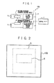
- FIG. 1 shows a general function block diagram of the device.
- the RF-ID device 100 includes an IC card function circuit 1, a reader/writer function circuit 2, a control circuit 3 to control these circuits 1 and 2, a control line 4 to connect these circuits 1 to 3 to each other, a receiving antenna 5, a transmitting antenna 6, a receiving resonance frequency adjuster circuit 7, and a transmitting resonance frequency adjuster circuit 8.
- the receiving antenna 5 is connected in parallel to the receiving resonance frequency adjuster circuit 7; the receiving antenna 5 and the receiving resonance frequency adjuster circuit 7 are adjusted to have a best communication distance characteristic in operation of the IC card function.
- the transmitting antenna 6 is connected in series to the transmitting resonance frequency adjuster circuit 8; the antenna 6 and the transmitting resonance frequency adjuster circuit 8 are adjusted to have a best communication distance characteristic in operation of the reader/writer function.
- the RF-ID device 100 of this kind to improve the communication characteristic in the IC card function, it is required to increase the area and the number of turns of the receiving antenna 5. On the other hand, to improve the communication characteristic in the reader/writer function, it is required to reduce the area and the number of turns of the transmitting antenna 6. Hence, it is necessary to independently and individually mount each of these antennas in the device 100. Specifically, referring to FIG. 2 which is a mounting plan view of the RF-ID device 100, there is employed a contour in which the transmitting antenna 6 is installed in the form of a loop on the inner side of the loop of the receiving antenna 5.
- the antenna for the IC card function is mutually opposite in the characteristic to the antenna for the reader/writer function; as shown in FIG. 2 , the antenna mounting area becomes larger; this hence inevitably leads to usage of a quite disadvantageous mounting scheme in recent portable communication apparatuses having a downsizing tendency.
- Patent Document 1 there is disclosed a technique in which in a communication apparatus including an IC card function and a reader/writer function, an antenna is commonly used for both functions. According to this technique, in the common use of the antenna for both functions, if one of the functions is in execution, the system inhibits execution of the other function to suppress interference of radio waves to be communicated therebetween.
- An exemplary object of the present invention is to provide a portable communication apparatus in which when commonly using a receiving antenna and a transmitting antenna having mutually opposing characteristics, the antennas can be commonly used without deteriorating the characteristics of both antennas.
- a communication apparatus includes: a first communication function module for performing contactless communication with an external first contactless communication device; a second communication function module including a communication function equal to a communication function of the first communication function module for performing contactless communication with an external second contactless communication device including a communication function equal to a communication function of the first contactless communication device; a common antenna shared between the first and second communication function modules; and resonance frequency switching means for changing a resonance frequency of the common antenna for each of the first and second communication function modules.
- the resonance frequency switching means may automatically change a resonance frequency at operation of each of the first and second communication function modules.
- the first communication module may be an RF-ID tag and the second communication module may be a reader/writer device which communicates with the RF-ID tag.
- the common antenna may be in the shape of a loop and circuit parts may be mounted in a loop of the common antenna. Moreover, the common antenna may be mounted on a printed board with a magnetic material therebetween.
- a portable communication terminal includes the communication apparatus constructed as above.
- a first advantage in accordance with the present invention resides in that the transmitting and receiving antenna is commonly used by disposing a transmitting and receiving resonance frequency switching function, and hence the common use can be implemented without deteriorating the respective characteristics of both antennas, and a saving of the mounting area is possible.
- a second advantage in accordance with the present invention resides in that since the transmitting and receiving antenna is commonly employed, other circuit parts can be installed in open portions in the loop-shaped antennas, and hence a saving of the mounting area is further enhanced.
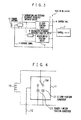
- FIG. 3 is a general function block diagram of the exemplary embodiment, and the equivalent components as those of FIG. 1 are assigned with the same reference numerals.
- An RF-ID device 100 of the exemplary embodiment includes an IC card function circuit 1, a reader/writer function circuit 2, a control circuit 3 to control the respective circuits 1 and 2, a control line 4 to connect each of these circuits 1 to 3 to each other, a transmitting resonance frequency adjuster circuit 8, a common antenna 10, and a transmitting and receiving resonance frequency switching circuit 11.
- the transmitting resonance frequency adjuster circuit 8 is connected in series to the common antenna 10 to lower impedance viewed from the reader/writer function circuit 2.
- the transmitting and receiving resonance frequency switching circuit 11 is connected in parallel to the common antenna 10 to change a transmitting and receiving resonance frequency based on a control signal 12 from the control circuit 3.
- a concrete example of the transmitting and receiving resonance frequency switching circuit 11 is shown in FIG. 4 .
- a switch SW is controlled for a switching operation by the control signal 12 from the control circuit 3 and selects either one of condensers C1 and C2 to connect the selected one thereof in parallel to the common antenna 10.
- the condenser C1 is a condenser for the IC card function and the condenser C2 is a condenser for the reader/writer function.
- a parallel resonance frequency of the condenser C 1 and the common antenna 10 depends on the communication characteristic of the RF-ID device 100 and the external reader/writer device; hence, the value fic is determined to make the communication characteristic favorable. Based on this value fic, the condenser C1 for the IC card function is determined. On the other hand, when the condenser C2 for the reader/writer function has relatively small capacity, there is obtained a communication distance characteristic between the RF-ID device 100 and an external IC card (not shown); hence, the capacity value of the condenser C2 is determined at a point where the communication distance is favorable.
- the common antenna 10 is automatically connected in parallel to the condenser C1 of the transmitting and receiving resonance frequency switching circuit 11.
- an external reader/writer device employed in, for example, a wicket of a transport facility
- data modulated in a predetermined modulation scheme is received via the common antenna 10 to be demodulated by the IC card function circuit 1 such that required data is sent via the control line 4 to the control circuit 3.
- a response from the IC card function circuit 1 to the external reader/writer device is carried out by using a load modulation different from the modulation scheme above.
- the common antenna 10 is automatically connected in parallel to the condenser C2 of the transmitting and receiving resonance frequency switching circuit 11.
- modulated data modulated using the predetermined modulation scheme is outputted from the reader/writer function circuit 2 such that data is transferred via the common antenna 10 to the IC card.
- the response is received via the common antenna 10 by the IC card function circuit 1.
- FIGS. 5 and 6 are diagrams to explain a method of mounting the common antenna 10 in which FIG. 5 is a perspective view thereof and FIG. 6 is a cross-sectional view thereof.
- the common antenna 10 can be produced using a Flexible Printed Circuit (FPC), a printed board, copper wire, and the like.
- FPC Flexible Printed Circuit
- the common antenna 10 is formed in the shape of a loop.
- the RF-ID device 100 is mounted in a communication apparatus such as a portable communication terminal with a severe mounting condition, since the distance between the common antenna 10 and a printed board 20 on which circuits are installed is quite small, inductance of the common antenna 10 is influenced by ground wiring of the printed board 20; hence, a magnetic sheet 21 is arranged below the common antenna 10.
- the common antenna 10 is disposed on the printed board 20, the common antenna 10 may also be arranged on metal such as a battery pack.
- FIGS. 7 and 8 are diagrams showing another method of mounting the common antenna 10; FIG. 7 is a perspective view thereof and FIG. 8 is a cross-sectional view thereof. In both diagrams, the equivalent components are assigned with the same reference numerals.
- an opening is disposed in a central portion of the common antenna 10 and the magnetic sheet 21, and circuit parts 22 are mounted in the opening region.
- the inner portion of the loop of the antenna 10 can be effectively used, which is quite suitable for a small-sized communication apparatus.
- the communication distance is deteriorated in the reader/writer function when compared with a case wherein the opening is not disposed as shown in FIGS. 5 and 6 .
- This deterioration can be compensated by adjusting the capacity of the condenser C2 for the reader/writer function to make the communication distance favorable.
- the present invention is applied to a communication apparatus including an IC card (RF-ID tag) function to achieve contactless communication of information with an external reader/writer device and a reader/writer function to carry out contactless communication of information with an external IC card and is additionally applicable to portable communication terminals (a cellular, a portable digital camera, a portable digital acoustic device, a Personal Digital Assistant (PDA), and the like) including the communication apparatus.
- IC card RFID tag
- PDA Personal Digital Assistant
Landscapes
- Engineering & Computer Science (AREA)
- Physics & Mathematics (AREA)
- General Physics & Mathematics (AREA)
- Theoretical Computer Science (AREA)
- Health & Medical Sciences (AREA)
- Microelectronics & Electronic Packaging (AREA)
- Computer Hardware Design (AREA)
- Toxicology (AREA)
- Artificial Intelligence (AREA)
- Computer Vision & Pattern Recognition (AREA)
- Electromagnetism (AREA)
- General Health & Medical Sciences (AREA)
- Near-Field Transmission Systems (AREA)
Abstract
Description
- The present invention relates to a communication apparatus and a portable communication terminal using the same, and in particular, to a communication apparatus including both of an RF-ID tag (IC card) function having a contactless communication function and a reader/writer function and a portable communication terminal using the same.
- There exists a Radio-Frequency Identification (RF-ID) device including an IC card function and a reader/writer function;
FIG. 1 shows a general function block diagram of the device. Referring toFIG. 1 , the RF-ID device 100 includes an ICcard function circuit 1, a reader/writer function circuit 2, a control circuit 3 to control thesecircuits control line 4 to connect thesecircuits 1 to 3 to each other, a receivingantenna 5, a transmittingantenna 6, a receiving resonancefrequency adjuster circuit 7, and a transmitting resonancefrequency adjuster circuit 8. - The
receiving antenna 5 is connected in parallel to the receiving resonancefrequency adjuster circuit 7; the receivingantenna 5 and the receiving resonancefrequency adjuster circuit 7 are adjusted to have a best communication distance characteristic in operation of the IC card function. Moreover, the transmittingantenna 6 is connected in series to the transmitting resonancefrequency adjuster circuit 8; theantenna 6 and the transmitting resonancefrequency adjuster circuit 8 are adjusted to have a best communication distance characteristic in operation of the reader/writer function. - Description will be given of data communication in the operation for the IC card (RF-ID tag) function. In communication with an external reader/writer device (not shown) installed in, for example, a ticket gate of a transport facility, received data which is modulated in a predetermined modulation scheme and which is outputted from the external reader/writer device is received via the
receiving antenna 5 and is inputted to the ICcard function circuit 1 to be demodulated such that required data is supplied via thecontrol line 4 to the control circuit 3. A response from the ICcard function circuit 1 to the external reader/writer device is conducted using a load modulation which is different from the modulation scheme above and which less consumes power. - Next, description will be given of data communication in the operation for the reader/writer function. In communication with an external contactless IC card (not shown), modulated data which is modulated in the predetermined modulation scheme described above is outputted from the reader/
writer function circuit 2 such that data is transferred via the transmittingantenna 6 to the IC card. In operation of a response using the load modulation from the external contactless IC card, data is received via thereceiving antenna 5 by the ICcard function circuit 1. - In the RF-
ID device 100 of this kind, to improve the communication characteristic in the IC card function, it is required to increase the area and the number of turns of the receivingantenna 5. On the other hand, to improve the communication characteristic in the reader/writer function, it is required to reduce the area and the number of turns of the transmittingantenna 6. Hence, it is necessary to independently and individually mount each of these antennas in thedevice 100. Specifically, referring toFIG. 2 which is a mounting plan view of the RF-ID device 100, there is employed a contour in which the transmittingantenna 6 is installed in the form of a loop on the inner side of the loop of thereceiving antenna 5. - In this way, the antenna for the IC card function is mutually opposite in the characteristic to the antenna for the reader/writer function; as shown in
FIG. 2 , the antenna mounting area becomes larger; this hence inevitably leads to usage of a quite disadvantageous mounting scheme in recent portable communication apparatuses having a downsizing tendency. - Now, referring to
Patent Document 1, there is disclosed a technique in which in a communication apparatus including an IC card function and a reader/writer function, an antenna is commonly used for both functions. According to this technique, in the common use of the antenna for both functions, if one of the functions is in execution, the system inhibits execution of the other function to suppress interference of radio waves to be communicated therebetween. Patent Document: Japanese Patent Laid-Open Publication Ser. No.2006-067448 - According to the technique of
Patent Document 1 described above, although the structure to commonly use the antenna for the IC card function and the reader/writer function is disclosed, there has not been disclosed any specific configuration for the common use of the antennas. As above, the antennas of both functions are mutually opposite in the characteristic; hence, only by simply adopting the common use, the required Rf characteristic cannot be obtained; hence, there is desired specific implementation means to commonly use the antennas without deteriorating the characteristics of both antennas. - An exemplary object of the present invention is to provide a portable communication apparatus in which when commonly using a receiving antenna and a transmitting antenna having mutually opposing characteristics, the antennas can be commonly used without deteriorating the characteristics of both antennas.
- A communication apparatus according to an exemplary aspect of the present invention includes: a first communication function module for performing contactless communication with an external first contactless communication device; a second communication function module including a communication function equal to a communication function of the first communication function module for performing contactless communication with an external second contactless communication device including a communication function equal to a communication function of the first contactless communication device; a common antenna shared between the first and second communication function modules; and resonance frequency switching means for changing a resonance frequency of the common antenna for each of the first and second communication function modules.
- And, the resonance frequency switching means may automatically change a resonance frequency at operation of each of the first and second communication function modules. Furthermore, the first communication module may be an RF-ID tag and the second communication module may be a reader/writer device which communicates with the RF-ID tag.
- Additionally, the common antenna may be in the shape of a loop and circuit parts may be mounted in a loop of the common antenna. Moreover, the common antenna may be mounted on a printed board with a magnetic material therebetween.
- Also, a portable communication terminal according to an exemplary aspect of the present invention includes the communication apparatus constructed as above.
- A first advantage in accordance with the present invention resides in that the transmitting and receiving antenna is commonly used by disposing a transmitting and receiving resonance frequency switching function, and hence the common use can be implemented without deteriorating the respective characteristics of both antennas, and a saving of the mounting area is possible.
- A second advantage in accordance with the present invention resides in that since the transmitting and receiving antenna is commonly employed, other circuit parts can be installed in open portions in the loop-shaped antennas, and hence a saving of the mounting area is further enhanced.
- Referring next to drawings, description will be given of an exemplary embodiment of the present invention.
FIG. 3 is a general function block diagram of the exemplary embodiment, and the equivalent components as those ofFIG. 1 are assigned with the same reference numerals. An RF-ID device 100 of the exemplary embodiment includes an ICcard function circuit 1, a reader/writer function circuit 2, a control circuit 3 to control therespective circuits control line 4 to connect each of thesecircuits 1 to 3 to each other, a transmitting resonancefrequency adjuster circuit 8, acommon antenna 10, and a transmitting and receiving resonancefrequency switching circuit 11. - The transmitting resonance
frequency adjuster circuit 8 is connected in series to thecommon antenna 10 to lower impedance viewed from the reader/writer function circuit 2. The transmitting and receiving resonancefrequency switching circuit 11 is connected in parallel to thecommon antenna 10 to change a transmitting and receiving resonance frequency based on acontrol signal 12 from the control circuit 3. A concrete example of the transmitting and receiving resonancefrequency switching circuit 11 is shown inFIG. 4 . - In
FIG. 4 , a switch SW is controlled for a switching operation by thecontrol signal 12 from the control circuit 3 and selects either one of condensers C1 and C2 to connect the selected one thereof in parallel to thecommon antenna 10. The condenser C1 is a condenser for the IC card function and the condenser C2 is a condenser for the reader/writer function. - A parallel resonance frequency of the
condenser C 1 and thecommon antenna 10 depends on the communication characteristic of the RF-ID device 100 and the external reader/writer device; hence, the value fic is determined to make the communication characteristic favorable. Based on this value fic, the condenser C1 for the IC card function is determined. On the other hand, when the condenser C2 for the reader/writer function has relatively small capacity, there is obtained a communication distance characteristic between the RF-ID device 100 and an external IC card (not shown); hence, the capacity value of the condenser C2 is determined at a point where the communication distance is favorable. - Description will be given of data communication in the operation for the IC card (RF-ID tag) function. In the operation, the
common antenna 10 is automatically connected in parallel to the condenser C1 of the transmitting and receiving resonancefrequency switching circuit 11. For example, in communication with an external reader/writer device employed in, for example, a wicket of a transport facility, data modulated in a predetermined modulation scheme is received via thecommon antenna 10 to be demodulated by the ICcard function circuit 1 such that required data is sent via thecontrol line 4 to the control circuit 3. A response from the ICcard function circuit 1 to the external reader/writer device is carried out by using a load modulation different from the modulation scheme above. - Next, description will be given of data communication in the operation for the reader/writer function. In this operation, the
common antenna 10 is automatically connected in parallel to the condenser C2 of the transmitting and receiving resonancefrequency switching circuit 11. In communication with a general contactless IC card (RF-ID tag), modulated data modulated using the predetermined modulation scheme is outputted from the reader/writer function circuit 2 such that data is transferred via thecommon antenna 10 to the IC card. When conducting a response from the IC card using the load modulation, the response is received via thecommon antenna 10 by the ICcard function circuit 1. -
FIGS. 5 and 6 are diagrams to explain a method of mounting thecommon antenna 10 in whichFIG. 5 is a perspective view thereof andFIG. 6 is a cross-sectional view thereof. As shown in these diagrams, thecommon antenna 10 can be produced using a Flexible Printed Circuit (FPC), a printed board, copper wire, and the like. As shown inFIG. 5 , thecommon antenna 10 is formed in the shape of a loop. - In a case wherein the RF-
ID device 100 is mounted in a communication apparatus such as a portable communication terminal with a severe mounting condition, since the distance between thecommon antenna 10 and a printedboard 20 on which circuits are installed is quite small, inductance of thecommon antenna 10 is influenced by ground wiring of the printedboard 20; hence, amagnetic sheet 21 is arranged below thecommon antenna 10. Incidentally, in this example, although thecommon antenna 10 is disposed on the printedboard 20, thecommon antenna 10 may also be arranged on metal such as a battery pack. -
FIGS. 7 and 8 are diagrams showing another method of mounting thecommon antenna 10;FIG. 7 is a perspective view thereof andFIG. 8 is a cross-sectional view thereof. In both diagrams, the equivalent components are assigned with the same reference numerals. In this example, an opening is disposed in a central portion of thecommon antenna 10 and themagnetic sheet 21, andcircuit parts 22 are mounted in the opening region. As a result, the inner portion of the loop of theantenna 10 can be effectively used, which is quite suitable for a small-sized communication apparatus. - In a case wherein the opening is disposed in the
common antenna 10 and themagnetic sheet 21, the communication distance is deteriorated in the reader/writer function when compared with a case wherein the opening is not disposed as shown inFIGS. 5 and 6 . This deterioration can be compensated by adjusting the capacity of the condenser C2 for the reader/writer function to make the communication distance favorable. - The present invention is applied to a communication apparatus including an IC card (RF-ID tag) function to achieve contactless communication of information with an external reader/writer device and a reader/writer function to carry out contactless communication of information with an external IC card and is additionally applicable to portable communication terminals (a cellular, a portable digital camera, a portable digital acoustic device, a Personal Digital Assistant (PDA), and the like) including the communication apparatus.
- This application is based upon and claims the benefit of priority from Japanese patent application No.
2006-289335, filed on October 25, 2006 -
- [
FIG. 1 ] is a general function block diagram showing a related art; - [
FIG. 2 ] is a plan view showing a mounting example of theantennas FIG. 1 ; - [
FIG. 3 ] is a general function block diagram showing an exemplary embodiment of the present invention; - [
FIG. 4 ] is a diagram showing an example of the transmitting and receiving resonance frequency switching circuit; - [
FIG. 5 ] is a perspective view showing a mounting example of thecommon antenna 10 in the exemplary embodiment of the present invention; - [
FIG. 6 ] is a cross-sectional view showing a mounting example of thecommon antenna 10 in the exemplary embodiment of the present invention; - [
FIG. 7 ] is a perspective view showing another mounting example of thecommon antenna 10 in the exemplary embodiment of the present invention; and - [
FIG. 8 ] is a cross-sectional view showing another mounting example of thecommon antenna 10 in the exemplary embodiment of the present invention. -
- 1 IC card (RF-ID tag) function circuit
- 2 Reader/writer function circuit
- 3 Control circuit
- 4 Control line
- 8 Transmitting resonance frequency adjuster circuit
- 10 Common (shared) antenna
- 11 Transmitting and receiving resonance frequency switching circuit
- 12 Control signal
- 20 Printed board
- 21 Magnetic sheet
- 100 RF-ID device
- SW Switch
- C1, C2 Condenser
Claims (8)
- A communication apparatus comprising:a first communication function module for performing contactless communication with an external first contactless communication device;a second communication function module including a communication function equal to a communication function of the first communication function module for performing contactless communication with an external second contactless communication device including a communication function equal to a communication function of the first contactless communication device;a common antenna shared between the first and second communication function modules; andresonance frequency switching means for changing a resonance frequency of the common antenna for each of the first and second communication function modules.
- The communication apparatus in accordance with claim 1, wherein the resonance frequency switching means automatically change a resonance frequency at operation of each of the first and second communication function modules.
- The communication apparatus in accordance with claim 1 or 2, wherein the first communication module is an RF-ID tag and the second communication module is a reader/writer device which communicates with the RF-ID tag.
- The communication apparatus in accordance with one of claims 1 to 3, wherein the common antenna is in the shape of a loop.
- The communication apparatus in accordance with claim 4, wherein circuit parts are mounted in a loop of the common antenna.
- The communication apparatus in accordance with one of claims 1 to 5, wherein the common antenna is mounted on a printed board with a magnetic material therebetween.
- A portable communication terminal comprising a communication apparatus in accordance with one of claims 1 to 6.
- A communication method comprising:performing contactless communication with an external first contactless communication apparatus;performing contactless communication with an external second contactless communication apparatus; andperforming contactless communication via a common antenna with the first and second contactless communication apparatuses by changing a resonance frequency.
Applications Claiming Priority (2)
| Application Number | Priority Date | Filing Date | Title |
|---|---|---|---|
| JP2006289335A JP4977438B2 (en) | 2006-10-25 | 2006-10-25 | Communication device and portable communication terminal using the same |
| EP07830405A EP2088538A4 (en) | 2006-10-25 | 2007-10-23 | Communication device and portable communication terminal using the same |
Related Parent Applications (1)
| Application Number | Title | Priority Date | Filing Date |
|---|---|---|---|
| EP07830405A Division EP2088538A4 (en) | 2006-10-25 | 2007-10-23 | Communication device and portable communication terminal using the same |
Publications (1)
| Publication Number | Publication Date |
|---|---|
| EP2793174A1 true EP2793174A1 (en) | 2014-10-22 |
Family
ID=39324574
Family Applications (2)
| Application Number | Title | Priority Date | Filing Date |
|---|---|---|---|
| EP20140171287 Ceased EP2793174A1 (en) | 2006-10-25 | 2007-10-23 | Communication device and portable communication terminal using the same |
| EP07830405A Withdrawn EP2088538A4 (en) | 2006-10-25 | 2007-10-23 | Communication device and portable communication terminal using the same |
Family Applications After (1)
| Application Number | Title | Priority Date | Filing Date |
|---|---|---|---|
| EP07830405A Withdrawn EP2088538A4 (en) | 2006-10-25 | 2007-10-23 | Communication device and portable communication terminal using the same |
Country Status (5)
| Country | Link |
|---|---|
| US (2) | US8125337B2 (en) |
| EP (2) | EP2793174A1 (en) |
| JP (1) | JP4977438B2 (en) |
| CN (1) | CN101529449B (en) |
| WO (1) | WO2008050777A1 (en) |
Cited By (1)
| Publication number | Priority date | Publication date | Assignee | Title |
|---|---|---|---|---|
| CN106056019A (en) * | 2016-05-24 | 2016-10-26 | 北京工业大学 | High-temperature-resistant low-frequency antenna and discrete device drive amplification circuit thereof |
Families Citing this family (13)
| Publication number | Priority date | Publication date | Assignee | Title |
|---|---|---|---|---|
| JP2009135710A (en) * | 2007-11-29 | 2009-06-18 | Toshiba Corp | Wireless device and antenna device |
| JP2009176027A (en) * | 2008-01-24 | 2009-08-06 | Toshiba Corp | Wireless communication apparatus and wireless communication system |
| JP2010098600A (en) * | 2008-10-17 | 2010-04-30 | Panasonic Corp | Non-contact communication device |
| US8682261B2 (en) * | 2009-02-13 | 2014-03-25 | Qualcomm Incorporated | Antenna sharing for wirelessly powered devices |
| JP5640655B2 (en) * | 2010-10-29 | 2014-12-17 | ソニー株式会社 | Portable communication device, reader / writer device, and resonance frequency adjusting method |
| JP5626043B2 (en) * | 2011-03-10 | 2014-11-19 | 株式会社村田製作所 | RFID reader / writer with RFID tag function and RFID reader / writer module with RFID tag function |
| US8917160B2 (en) * | 2011-03-21 | 2014-12-23 | Sony Corporation | RFID module |
| CN102739291B (en) * | 2011-04-02 | 2014-08-13 | 国民技术股份有限公司 | Near field communication module, system and method thereof |
| FR2988195B1 (en) * | 2012-03-14 | 2015-04-10 | Continental Automotive France | NEAR-FIELD DETECTION AND COMMUNICATION DEVICE |
| KR102022867B1 (en) * | 2012-08-07 | 2019-09-20 | 삼성전자 주식회사 | Near field communication circuit and operating method of the same |
| SK288677B6 (en) * | 2015-06-02 | 2019-06-04 | Logomotion, S.R.O. | A method of processing a signal transmitted from an NFC analog driver and engaging it in execution |
| CN107066907A (en) * | 2016-12-19 | 2017-08-18 | 徐学军 | Merchandise control and the method purchased again |
| CN112084797A (en) * | 2020-08-21 | 2020-12-15 | 中国人民解放军海军工程大学 | A handheld terminal device for identifying special materials |
Citations (5)
| Publication number | Priority date | Publication date | Assignee | Title |
|---|---|---|---|---|
| WO2005008575A1 (en) * | 2003-07-22 | 2005-01-27 | Nokia Corporation | Reader device for radio frequency identification transponder with transponder functionality |
| EP1560149A2 (en) * | 2004-01-30 | 2005-08-03 | Sony Corporation | Portable type information processing terminal device |
| JP2006067448A (en) | 2004-08-30 | 2006-03-09 | Ricoh Co Ltd | COMMUNICATION DEVICE AND PORTABLE ELECTRONIC DEVICE HAVING THE COMMUNICATION DEVICE |
| GB2421663A (en) * | 2005-04-11 | 2006-06-28 | Innovision Res & Tech Plc | Communications apparatus having a short-range wireless RF communicator and a high data-rate communicator |
| EP1696362A1 (en) * | 2005-02-28 | 2006-08-30 | Kabushiki Kaisha Toshiba | Radio communication device, radio communication method and non-contact IC card reader/writer device |
Family Cites Families (12)
| Publication number | Priority date | Publication date | Assignee | Title |
|---|---|---|---|---|
| JPH04278691A (en) | 1991-03-06 | 1992-10-05 | Omron Corp | Non-contact type pass gate system |
| US5942977A (en) * | 1997-08-13 | 1999-08-24 | Ludwig Kipp | Radio transponder |
| US6351215B2 (en) * | 1998-06-02 | 2002-02-26 | Rf Code, Inc. | Monitoring antenna system |
| JP3669331B2 (en) | 2000-03-06 | 2005-07-06 | 三菱電機株式会社 | Transmitting and receiving antenna device |
| US6480110B2 (en) * | 2000-12-01 | 2002-11-12 | Microchip Technology Incorporated | Inductively tunable antenna for a radio frequency identification tag |
| JP4232434B2 (en) * | 2002-10-28 | 2009-03-04 | ソニー株式会社 | Semiconductor integrated circuit device, wireless communication terminal |
| JPWO2004073108A1 (en) * | 2003-02-14 | 2006-06-01 | 株式会社東芝 | Electronics |
| JP2005122595A (en) | 2003-10-20 | 2005-05-12 | Matsushita Electric Ind Co Ltd | Proximity contactless communication equipment |
| JP2006025155A (en) * | 2004-07-07 | 2006-01-26 | Sony Corp | Communication device and semiconductor integrated circuit |
| JP4618672B2 (en) * | 2004-09-02 | 2011-01-26 | フェリカネットワークス株式会社 | Semiconductor integrated circuit and wireless communication device |
| JP4496105B2 (en) * | 2005-02-28 | 2010-07-07 | 株式会社東芝 | Wireless communication device |
| JP4812322B2 (en) | 2005-04-08 | 2011-11-09 | パナソニック株式会社 | Mobile communication device |
-
2006
- 2006-10-25 JP JP2006289335A patent/JP4977438B2/en active Active
-
2007
- 2007-10-23 US US12/447,090 patent/US8125337B2/en not_active Expired - Fee Related
- 2007-10-23 EP EP20140171287 patent/EP2793174A1/en not_active Ceased
- 2007-10-23 EP EP07830405A patent/EP2088538A4/en not_active Withdrawn
- 2007-10-23 CN CN200780040112.8A patent/CN101529449B/en not_active Expired - Fee Related
- 2007-10-23 WO PCT/JP2007/070671 patent/WO2008050777A1/en not_active Ceased
-
2012
- 2012-01-10 US US13/347,340 patent/US8373560B2/en not_active Expired - Fee Related
Patent Citations (5)
| Publication number | Priority date | Publication date | Assignee | Title |
|---|---|---|---|---|
| WO2005008575A1 (en) * | 2003-07-22 | 2005-01-27 | Nokia Corporation | Reader device for radio frequency identification transponder with transponder functionality |
| EP1560149A2 (en) * | 2004-01-30 | 2005-08-03 | Sony Corporation | Portable type information processing terminal device |
| JP2006067448A (en) | 2004-08-30 | 2006-03-09 | Ricoh Co Ltd | COMMUNICATION DEVICE AND PORTABLE ELECTRONIC DEVICE HAVING THE COMMUNICATION DEVICE |
| EP1696362A1 (en) * | 2005-02-28 | 2006-08-30 | Kabushiki Kaisha Toshiba | Radio communication device, radio communication method and non-contact IC card reader/writer device |
| GB2421663A (en) * | 2005-04-11 | 2006-06-28 | Innovision Res & Tech Plc | Communications apparatus having a short-range wireless RF communicator and a high data-rate communicator |
Cited By (2)
| Publication number | Priority date | Publication date | Assignee | Title |
|---|---|---|---|---|
| CN106056019A (en) * | 2016-05-24 | 2016-10-26 | 北京工业大学 | High-temperature-resistant low-frequency antenna and discrete device drive amplification circuit thereof |
| CN106056019B (en) * | 2016-05-24 | 2019-06-14 | 北京工业大学 | A high-temperature and low-frequency antenna and its drive amplifier circuit system for discrete devices |
Also Published As
| Publication number | Publication date |
|---|---|
| JP4977438B2 (en) | 2012-07-18 |
| US20120105209A1 (en) | 2012-05-03 |
| US8125337B2 (en) | 2012-02-28 |
| US20100001839A1 (en) | 2010-01-07 |
| WO2008050777A1 (en) | 2008-05-02 |
| US8373560B2 (en) | 2013-02-12 |
| CN101529449A (en) | 2009-09-09 |
| JP2008108016A (en) | 2008-05-08 |
| EP2088538A4 (en) | 2011-11-09 |
| EP2088538A1 (en) | 2009-08-12 |
| CN101529449B (en) | 2016-08-17 |
Similar Documents
| Publication | Publication Date | Title |
|---|---|---|
| US8373560B2 (en) | Communication apparatus and portable communication terminal using the same | |
| EP1641140B1 (en) | Data communication device | |
| US8406686B2 (en) | Wireless communication terminal apparatus and method of controlling same | |
| JP4393228B2 (en) | Small antenna and wireless tag provided with the same | |
| EP3550731B1 (en) | Nfc antenna in a mobile device | |
| US9016592B2 (en) | Antenna device and communication terminal apparatus | |
| KR101232557B1 (en) | Mobile radio device | |
| EP1826866A1 (en) | Antenna and noncontact tag | |
| JP2001344574A (en) | Interrogator antenna device | |
| US8400362B2 (en) | Radio communication apparatus and method for making radio communication apparatus | |
| EP2458530A1 (en) | Transponder tagged object and method for its manufacturing | |
| KR20080007181A (en) | Contactless communication circuits and portable terminals | |
| JP2005165703A (en) | Non-contact identification medium | |
| US8041295B2 (en) | Mobile communication device | |
| JP2011015005A (en) | Antenna device, and portable wireless apparatus provided with the same | |
| CN211655071U (en) | Card type radio communication apparatus | |
| JP2006262055A (en) | Antenna module and portable information terminal having the same | |
| EP2490294A1 (en) | Transmission/reception antenna and transmission/reception device using same | |
| KR101494148B1 (en) | Parallel antenna and tag with the parallel antenna | |
| US7729660B2 (en) | Communication device, non-contact type IC card mounting same, and information apparatus | |
| JP2011165151A (en) | Radio communication device and noncontact communication antenna used for the same | |
| EP2323220A1 (en) | Antenna device | |
| CN112510347A (en) | Antenna module |
Legal Events
| Date | Code | Title | Description |
|---|---|---|---|
| PUAI | Public reference made under article 153(3) epc to a published international application that has entered the european phase |
Free format text: ORIGINAL CODE: 0009012 |
|
| 17P | Request for examination filed |
Effective date: 20140605 |
|
| AC | Divisional application: reference to earlier application |
Ref document number: 2088538 Country of ref document: EP Kind code of ref document: P |
|
| AK | Designated contracting states |
Kind code of ref document: A1 Designated state(s): AT BE BG CH CY CZ DE DK EE ES FI FR GB GR HU IE IS IT LI LT LU LV MC MT NL PL PT RO SE SI SK TR |
|
| R17P | Request for examination filed (corrected) |
Effective date: 20150422 |
|
| RBV | Designated contracting states (corrected) |
Designated state(s): AT BE BG CH CY CZ DE DK EE ES FI FR GB GR HU IE IS IT LI LT LU LV MC MT NL PL PT RO SE SI SK TR |
|
| 17Q | First examination report despatched |
Effective date: 20151105 |
|
| STAA | Information on the status of an ep patent application or granted ep patent |
Free format text: STATUS: THE APPLICATION HAS BEEN REFUSED |
|
| 18R | Application refused |
Effective date: 20161128 |