EP2790268A1 - Multi-band antenna - Google Patents
Multi-band antenna Download PDFInfo
- Publication number
- EP2790268A1 EP2790268A1 EP13305482.5A EP13305482A EP2790268A1 EP 2790268 A1 EP2790268 A1 EP 2790268A1 EP 13305482 A EP13305482 A EP 13305482A EP 2790268 A1 EP2790268 A1 EP 2790268A1
- Authority
- EP
- European Patent Office
- Prior art keywords
- feed
- radiating element
- radiating
- band
- feed element
- Prior art date
- Legal status (The legal status is an assumption and is not a legal conclusion. Google has not performed a legal analysis and makes no representation as to the accuracy of the status listed.)
- Withdrawn
Links
Images




Classifications
-
- H—ELECTRICITY
- H01—ELECTRIC ELEMENTS
- H01Q—ANTENNAS, i.e. RADIO AERIALS
- H01Q9/00—Electrically-short antennas having dimensions not more than twice the operating wavelength and consisting of conductive active radiating elements
- H01Q9/04—Resonant antennas
- H01Q9/0407—Substantially flat resonant element parallel to ground plane, e.g. patch antenna
- H01Q9/0421—Substantially flat resonant element parallel to ground plane, e.g. patch antenna with a shorting wall or a shorting pin at one end of the element
-
- H—ELECTRICITY
- H01—ELECTRIC ELEMENTS
- H01Q—ANTENNAS, i.e. RADIO AERIALS
- H01Q1/00—Details of, or arrangements associated with, antennas
- H01Q1/12—Supports; Mounting means
- H01Q1/22—Supports; Mounting means by structural association with other equipment or articles
- H01Q1/2291—Supports; Mounting means by structural association with other equipment or articles used in Bluetooth® or Wi-Fi® devices of Wireless Local Area Networks [WLAN]
-
- H—ELECTRICITY
- H01—ELECTRIC ELEMENTS
- H01Q—ANTENNAS, i.e. RADIO AERIALS
- H01Q1/00—Details of, or arrangements associated with, antennas
- H01Q1/48—Earthing means; Earth screens; Counterpoises
-
- H—ELECTRICITY
- H01—ELECTRIC ELEMENTS
- H01Q—ANTENNAS, i.e. RADIO AERIALS
- H01Q21/00—Antenna arrays or systems
- H01Q21/30—Combinations of separate antenna units operating in different wavebands and connected to a common feeder system
-
- H—ELECTRICITY
- H01—ELECTRIC ELEMENTS
- H01Q—ANTENNAS, i.e. RADIO AERIALS
- H01Q5/00—Arrangements for simultaneous operation of antennas on two or more different wavebands, e.g. dual-band or multi-band arrangements
- H01Q5/40—Imbricated or interleaved structures; Combined or electromagnetically coupled arrangements, e.g. comprising two or more non-connected fed radiating elements
-
- H—ELECTRICITY
- H01—ELECTRIC ELEMENTS
- H01Q—ANTENNAS, i.e. RADIO AERIALS
- H01Q9/00—Electrically-short antennas having dimensions not more than twice the operating wavelength and consisting of conductive active radiating elements
- H01Q9/04—Resonant antennas
- H01Q9/30—Resonant antennas with feed to end of elongated active element, e.g. unipole
- H01Q9/42—Resonant antennas with feed to end of elongated active element, e.g. unipole with folded element, the folded parts being spaced apart a small fraction of the operating wavelength
Definitions
- the present invention relates generally to a multiband antenna for wireless communication systems, for example for home-networking devices or mobile devices.
- Home-networking devices such as gateways and set-top-boxes, needs to be compatible with more and more wireless standards.
- These standards are for example: WLAN (Wireless Local Area Network) operating in the 2.4 GHz and 5GHz band, Bluetooth and RF4CE (Radio Frequency For Consumer Electronics) operating in the 2.4GHz band, DECT (Digital Enhanced Cordless telecommunications) operating in the 1900MHz band, and LTE (Long Term Evolution) operating in the UHF and L bands.
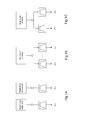
- Fig.1A to Fig.1C illustrate three possible antenna architectures.
- An object of the present invention is to propose a multi-band antenna that can be used according to the architecture of Fig.1C .
- Another object of the invention is to propose a compact low-cost multi-band antenna.
- Another object of the invention is to propose a multi-band antenna having performances comparable to those of a plurality of single band antennas.
- the multi-band antenna is created based on a plurality of printed inverted F antennas (PIFAs) which are superimposed and separated by a substrate layer.
- PIFAs printed inverted F antennas
- the invention concerns a multi-band antenna comprising
- the second conductive layer further comprises a second radiating element, a second feed element connected to said second radiating element and a second ground return element connected to said second radiating element and said first ground return element.
- the second ground return element is part of the ground section and the length of the second radiating element is different from the length of the first radiating element.
- the second radiating element and the second feed element are offset transversally from said first radiating element and said first feed element. This second radiating element, this second feed element and this second ground return element are arranged in order to form substantially a second printed inverted F antenna resonating in a second frequency band.
- These two PIFAs are for example created on a substrate having a top conductive layer and a bottom conductive layer.
- the radiating element and the feed element of the first PIFA are designed in the top conductive layer and the radiating element and the feed element of the second PIFA are designed in the bottom conductive layer.
- the first feed element and the second feed element are connected to a feed port.
- the multi-band antenna thus comprises only one signal input/output.
- each feed element is a connected to a separate feed port.
- the second feed element is preferably connected to the first feed element by a microstrip line printed in the second conductive layer and via-holes, said microstrip line being arranged below or above the first radiating element.
- the first ground return element is connected to the ground section by via holes.
- the second ground return element is connected to the first ground return element by said via holes.
- the first radiating element is a straight conductive line.
- the first radiating element comprises first and second successive straight portions, the second portion being perpendicular to the first portion.
- the length of the first radiating element is higher than the length of the second radiating element such that the second frequency band is higher than the first frequency band.
- the length and the width of the first feed element are defined to match the impedance of the first printed inverted F antenna with the impedance of a radio frequency circuit connected to the first feed element.
- the first feed element is connected to the radio frequency circuit via an inductor cascaded in series with a capacitor, the inductance of the inductor being determined in order to achieve impedance matching of the second printed inverted F antenna with the radio frequency circuit and the capacitance of the capacitor being determined in order to achieve impedance matching of the first printed inverted F antenna with the radio frequency circuit.
- the invention concerns also a multi-band antenna comprising more than two frequency bands.
- the antenna further comprises a third conductive layer of the substrate arranged between first and second conductive layers, said third conductive layer comprising a third radiating element, a third feed element connected to said third radiating element and a third ground return element connected to said third radiating element and said ground section, the length of the third radiating element being different from the lengths of said first and second radiating elements, said third radiating element and said third feed element being offset transversally from said first and second radiating elements, said first and second feed elements and said ground section.
- Said third radiating element, said third feed element and said third ground return element are arranged in order to form substantially a third printed inverted F antenna resonating in a third frequency band.
- a PIFA is printed in each one of the three conductive layer attached to the substrate.
- the first feed element, the second feed element and the third feed element are connected to a feed port.
- the second feed element is connected to the third feed element by a first microstrip line printed in the second conductive layer and via-holes, said first microstrip line being arranged below or above the third radiating element
- the first feed element is connected to the third feed element by a second microstrip line printed in the third conductive layer and via-holes, said second microstrip line being arranged below or above the first radiating element.
- one of said first and second conductive layers further comprises a third radiating element, a third feed element connected to said third radiating element and a third ground return element connected to said third radiating element and said ground section, the length of the third radiating element being different from the lengths of said first and second radiating elements, said third radiating element and said third feed element being offset transversally from said first and second radiating elements, said first and second feed elements and said ground section.
- Said third radiating element, said third feed element and said third ground return element are arranged in order to form substantially a third printed inverted F antenna resonating in a third frequency band.
- At least one of the conductive layers comprises at least two PIFAs.
- the invention relates to an antenna comprising a plurality of PIFAs.
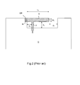
- Fig.2 shows the design of a single PIFA.
- This antenna is printed on a substrate having two conductive metal layers: a top layer (in hatched line) on which are printed a feed element F a radiating element R and a ground return element GR, and a bottom layer on which is printed a ground section or ground plane G.
- the radiating element R is basically made up of a rectangular line. It can be also meandered to reduce its length.
- the length L 0 of this element is substantially equal to a quarter of the wavelength at the center frequency of the targeted bandwidth of the antenna.
- the radiating element R is open-ended at one end and short-circuited to the ground section G by means of the ground return element GR and via-holes H at the other end.
- the radiating element and the feed element are offset transversally from the ground section G.
- the radiating element R is fed by the feed element F which is arranged perpendicularly to the radiating element, both elements together with the ground return element GR form with the vertical edge of the ground plane a kind of inverted-F shape.
- a PIFA designates an antenna having an inverted F shape or an antenna having a T shape.
- a multi-band antenna based on a plurality of PIFAs which are stacked above each other.
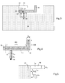
- Figures 3 to 6 illustrate a first embodiment of a dual-band antenna according to the invention.
- the dual band antenna is made on a substrate having two conductive metal layers: a top layer (in hatched line) attached to the top surface of the substrate and a bottom layer attached to the bottom layer of the substrate.
- the bottom layer comprises a ground section 10.
- a radiating element 30, a feed element 31 and a ground return element 32 are printed in the top layer.
- the radiating element 30 and the feed element 31 are offset transversally from the ground section 10.
- the radiating element 30 has an end connected to the ground section 10 by means of the ground return element 32 and via-holes 60.
- the other end of the radiating element 30 is open-ended.
- the feed element 31 is connected perpendicularly to the radiating element 30.
- the free end of the feed element 31 is connected to a feed port 80.
- the radiating element 30 comprises two successive rectangular portions, a first portion 30A and a second portion 30B which is perpendicular to the portion 30A.
- the radiating element 30, the feed element 31 and the ground return element 32 are arranged such that they form substantially a first printed inverted F antenna resonating in a first frequency band B1.
- the length L 30 of the radiating element 30 is substantially equal to ⁇ 1 /4, where ⁇ 1 is the wavelength at the center frequency of the band B1.
- the bottom layer comprises also a radiating element 20, a feed element 21 and a ground return element 22.
- the ground return element 22 is part of the ground section 10.
- the ground section 10 is shown in the figures by dots (area with dots).
- the radiating element 20 and the feed element 21 are offset transversally from the radiating element 30 and the feed element 31 of the top layer.
- the feed elements 21 and 31 are connected together via a microstrip line 50 printed in the bottom layer and via-holes 70. So, the two feed elements 21 and 31 are connected to the feed port 80.
- the radiating element 20, the feed element 21 and the ground return element 22 are arranged such that they form substantially a second printed inverted F antenna resonating in a second frequency band B2.
- the length L 20 of the radiating element 20 is substantially equal to ⁇ 2 /4, where ⁇ 2 is the wavelength at the center frequency of the band B2.
- the parameters of PIFA resonating in the frequency band B2 can be adjusted by acting on the following values:
- the length L 30 of the PIFA resonating in the frequency B1 is higher than the length L 20 of the PIFA resonating in the frequency B2 such that the band B1 is lower than the band B2.
- the PIFA constituted by the radiating element 30, the feed element 31 and the ground return element 32 forms the lower band PIFA and the PIFA constituted by the radiating element 20, the feed element 21 and the ground return element 22 forms the higher band PIFA.
- the width W 33 , the distance d 11 and the length L 31 of the feed element 31 are defined to match the impedance of the PIFA resonating in frequency Band B1 with the impedance of a radio frequency circuit connected to the feed port.
- the width W 31 and the length L 31 of the feed element 31 together with the width W 21 and the length L 21 of the feed element 21, the width W 50 of the microstrip line 50 and the distance d 21 are defined to match the impedance of the PIFA resonating in frequency Band B2 with the impedance of a radio frequency circuit connected to the feed port.
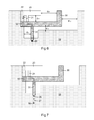
- the feed port 80 is connected to the radio frequency circuit via an inductor 26 cascaded in series with a capacitor 27, the inductance of the inductor 26 being determined in order to achieve impedance matching of the PIFA resonating in the higher band (band B2) with the radio frequency circuit and the capacitance of the capacitor 27 being determined in order to achieve impedance matching of the PIFA resonating in the lower band (band B1) with the radio frequency circuit.
- the radiating element 30 comprises a third straight portion 30C connected perpendicularly to the central portion 30A at the opposite of the portion 30B, the portions 30B and 30C extending in opposite directions.
- the via-holes 35 are placed at the free end of the portion C.
- the radiating element 30 comprises a plurality of straight portions forming meanders.
- the radiating element 30 comprises a single straight portion.
- a slot 11 is etched in the bottom layer in order to achieve for instance a narrower bandwidth in the higher frequency band.
- This dual-band antenna can be for example a WLAN dual-band 2.4/5GHz antenna.
- This antenna is for example printed onto a FR-4 substrate, the thickness of which is 1.2mm.
- the performances of such an antenna have been simulated by the HFSS TM 3D-EM simulation tool and are presented below.
- the simulated dual-band antenna comprises, at its input, an inductor 26 of 2.5 nH cascaded with a capacitor 27 of 0.7 pF.
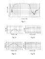
- Figs.11 to 19 show that the return loss levels are lower than the commonly required level (-10dB), in both bands [2.4GHz-2.5GHz] and [5.15 GHz-5.85GHz].
- Fig.12 and Fig.13 show that the simulated gain is at a fair level, at around 4dBi and 5dBi in the 2.4 GHz and 5GHz bands respectively.
- Fig.14 and Fig.15 show that the antenna exhibits a high efficiency in both frequency bands, around 80-85%.
- Fig.16 and Fig.17 show the 3D radiation patterns at 2.45 GHz and 5.5 GHz respectively. They are similar to what can exhibit a single band PIFA, with a radiation directed mainly to the front-side.
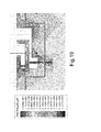
- Fig.18 and Fig.19 show of the current distributions at 2.45 GHz and 5.5 GHz respectively.
- Fig.18 points out that the radiating element 20, which resonates in the higher band, is not very activated, demonstrating by this way that this element is quite transparent in the 2.4GHz band.
- Fig.19 shows that the radiating element 20 is resonating while the radiating element 30 drives the residual current, as also the ground plane surrounding it.
- This topology of cascaded PIFAs can be extended to a multi-band antenna having more than two frequency bands. For example, it can be used for designing a 3-band antenna as illustrated by Figs.20 and 21 .
- the antenna of Figs.20 and 21 comprises a multi-layered substrate and three superimposed conductive layers, each one of these conductive layers being separated from an adjacent conductive layer by a substrate layer. These conductive layers are defined as bottom layer, intermediate layer and top layer. The bottom layer comprises the ground section 10.
- the antenna of Figs.20 and 21 comprises an additional PIFA resonating in a frequency band B3 different from B1 and B2 printed in the intermediate layer.
- the top layer comprises a first PIFA made of the radiating element 30, the feed element 31 and the ground return element 32.
- the bottom layer comprises a second PIFA made of the radiating element 20, the feed element 21 and the ground return element 22.
- the intermediate layer comprises a third PIFA made of a radiating element 40, a feed element 41 and a ground return element 42.
- the radiating element 30 is connected to the ground section 10 by means of the ground return element 32 and the via-holes 60.
- the radiating element 40 is connected to ground section 10 by means of the ground return element 42 and the via-holes 61.
- the ground return element 22 is connected to the ground return 42 by said via-holes 61.
- the feed element 21 is connected to the feed element 41 by means of a microstrip line 50a printed in the bottom layer and via-holes 70a and the feed element 41 is connected to the feed element 31 by means of a microstrip line 50b printed in the intermediate layer and via-holes 70b.
- the radiating element 30 resonates in a lower frequency band
- the radiating element 40 resonates in an intermediate frequency band
- the radiating element 20 resonates in a higher frequency band.
- each conductive layer comprises a single PIFA.
- one of the conductive layers comprises two PIFAs.
- the 3-band antenna comprises only two conductive layers, a bottom layer and a top layer.
- the PIFA made of the radiating element 20, the feed element 21 and the ground return element 22 is printed in the bottom layer and the two other PIFAs made of the radiating elements 30, 40, the feed elements 31, 41 and the ground return elements 32, 42 are printed in the top layer.
- the radiating element 30 is connected to the ground section 10 by means of the ground return element 32 and the via-holes 60.
- the radiating element 40 is connected to ground section 10 by means of the ground return element 42 and the via-holes 61. These elements are made in the top layer.
- the radiating element 20, the feed element 21 and the ground return element 22 made in the bottom layer are placed between the radiating element 40 and the radiating element 30.
- the ground return element 22 is directly connected to the ground section 10.
- the feed element 41 is connected to the feed element 21 by means of a microstrip line 51 printed in the top layer and via-holes 71 and the feed element 21 is connected to the feed element 31 by means of a microstrip line 50 printed in the bottom layer and via-holes 70.
Landscapes
- Engineering & Computer Science (AREA)
- Computer Networks & Wireless Communication (AREA)
- Physics & Mathematics (AREA)
- Electromagnetism (AREA)
- Waveguide Aerials (AREA)
- Variable-Direction Aerials And Aerial Arrays (AREA)
- Details Of Aerials (AREA)
Abstract
The present invention relates to multi-band antenna. This antenna comprises a substrate and first and a second conductive layer. According to the invention, each one of the first and second conductive layers comprises a PIFA resonating in specific frequency band. The PIFAs are cascaded in order to achieve a compact antenna. The first PIFA comprises a first radiating element (30), a first feed element (31) connected to said first radiating element and a first ground return element (32) and the second PIFA comprises a second radiating element (20), a second feed element (21) connected to said second radiating element and a second ground return element (22). The ground plane (10) is printed in the same layer than the second PIFA.
Description
- The present invention relates generally to a multiband antenna for wireless communication systems, for example for home-networking devices or mobile devices.
- Home-networking devices, such as gateways and set-top-boxes, needs to be compatible with more and more wireless standards. These standards are for example: WLAN (Wireless Local Area Network) operating in the 2.4 GHz and 5GHz band, Bluetooth and RF4CE (Radio Frequency For Consumer Electronics) operating in the 2.4GHz band, DECT (Digital Enhanced Cordless telecommunications) operating in the 1900MHz band, and LTE (Long Term Evolution) operating in the UHF and L bands.
- This demand of devices compatible with a plurality of wireless standards increases the number of requested antennas and subsequently increases the cost of devices. The demand of MIMO systems increases also the number of antennas. For a n-order MIMO system, n antennas are needed. In addition, the demand of radiation diversity for systems like RF4CE or DECT systems contributes also to this increase.
- Different antenna architectures are possible for these multiband wireless systems.
Fig.1A to Fig.1C illustrate three possible antenna architectures. -
Fig.1A shows a first antenna architecture comprising, for each requested band, a specific single band antenna and a specific filter. This solution is very costly since it requests a connector between each antenna and each filter. -
Fig.1B shows a second antenna architecture comprising a single wide band antenna and a specific filter for each requested band. In this architecture, the frequency bandwidth in which the antenna is well impedance-matched should cover all the frequency bands of the multiband system. A multiplexer is used in order to direct the signals towards the different filters and the associated transceivers. This solution is relatively cheap as it requests only one connector and one multiplexer. However, depending on the targeted frequency bandwidth, the design of this kind of antenna could be very tricky and could result in a trade-off solution between the size and the performances (return loss, gain, efficiency etc.). In addition, the wide band antenna can increase EMI issues because of its wide band gain. -
Fig.1C shows a third antenna architecture comprising a multi-band antenna and a specific filter for each requested band. With this kind of antenna, the antenna return loss response is multi-band. This means that the antenna is only well matched in the targeted frequency bands. This solution is low cost solution since it uses only one connector and one multiplexer. - An object of the present invention is to propose a multi-band antenna that can be used according to the architecture of
Fig.1C . - Another object of the invention is to propose a compact low-cost multi-band antenna.
- Another object of the invention is to propose a multi-band antenna having performances comparable to those of a plurality of single band antennas.
- According to the invention, the multi-band antenna is created based on a plurality of printed inverted F antennas (PIFAs) which are superimposed and separated by a substrate layer.
- More specifically, the invention concerns a multi-band antenna comprising
- a substrate;
- a first conductive layer and a second conductive layer separated from each other by said substrate, said second conductive layer comprising a ground section and said first conductive layer comprising a first radiating element, a first feed element connected to said first radiating element and a first ground return element connected to said first radiating element and said ground section, said first radiating element and said first feed element being offset transversally from the ground section,
- According to the invention, the second conductive layer further comprises a second radiating element, a second feed element connected to said second radiating element and a second ground return element connected to said second radiating element and said first ground return element. The second ground return element is part of the ground section and the length of the second radiating element is different from the length of the first radiating element. The second radiating element and the second feed element are offset transversally from said first radiating element and said first feed element. This second radiating element, this second feed element and this second ground return element are arranged in order to form substantially a second printed inverted F antenna resonating in a second frequency band.
- These two PIFAs are for example created on a substrate having a top conductive layer and a bottom conductive layer. The radiating element and the feed element of the first PIFA are designed in the top conductive layer and the radiating element and the feed element of the second PIFA are designed in the bottom conductive layer.
- In a specific embodiment of the invention, the first feed element and the second feed element are connected to a feed port. The multi-band antenna thus comprises only one signal input/output.
- As a variant, each feed element is a connected to a separate feed port.
- The second feed element is preferably connected to the first feed element by a microstrip line printed in the second conductive layer and via-holes, said microstrip line being arranged below or above the first radiating element.
- According to a specific feature of the invention, the first ground return element is connected to the ground section by via holes.
- According to another feature of the invention, the second ground return element is connected to the first ground return element by said via holes.
- In a specific embodiment of the invention, the first radiating element is a straight conductive line.
- In another embodiment, the first radiating element comprises first and second successive straight portions, the second portion being perpendicular to the first portion.
- In a specific embodiment of the invention, the length of the first radiating element is higher than the length of the second radiating element such that the second frequency band is higher than the first frequency band.
- Advantageously, the length and the width of the first feed element are defined to match the impedance of the first printed inverted F antenna with the impedance of a radio frequency circuit connected to the first feed element.
- Advantageously, the first feed element is connected to the radio frequency circuit via an inductor cascaded in series with a capacitor, the inductance of the inductor being determined in order to achieve impedance matching of the second printed inverted F antenna with the radio frequency circuit and the capacitance of the capacitor being determined in order to achieve impedance matching of the first printed inverted F antenna with the radio frequency circuit.
- The invention concerns also a multi-band antenna comprising more than two frequency bands.
- So, in a specific embodiment of the invention, the antenna further comprises a third conductive layer of the substrate arranged between first and second conductive layers, said third conductive layer comprising a third radiating element, a third feed element connected to said third radiating element and a third ground return element connected to said third radiating element and said ground section, the length of the third radiating element being different from the lengths of said first and second radiating elements, said third radiating element and said third feed element being offset transversally from said first and second radiating elements, said first and second feed elements and said ground section. Said third radiating element, said third feed element and said third ground return element are arranged in order to form substantially a third printed inverted F antenna resonating in a third frequency band.
- In this antenna, a PIFA is printed in each one of the three conductive layer attached to the substrate.
- According to a specific feature, the first feed element, the second feed element and the third feed element are connected to a feed port. For example, the second feed element is connected to the third feed element by a first microstrip line printed in the second conductive layer and via-holes, said first microstrip line being arranged below or above the third radiating element, and the first feed element is connected to the third feed element by a second microstrip line printed in the third conductive layer and via-holes, said second microstrip line being arranged below or above the first radiating element.
- In another embodiment of the invention, one of said first and second conductive layers further comprises a third radiating element, a third feed element connected to said third radiating element and a third ground return element connected to said third radiating element and said ground section, the length of the third radiating element being different from the lengths of said first and second radiating elements, said third radiating element and said third feed element being offset transversally from said first and second radiating elements, said first and second feed elements and said ground section. Said third radiating element, said third feed element and said third ground return element are arranged in order to form substantially a third printed inverted F antenna resonating in a third frequency band.
- In this embodiment, at least one of the conductive layers comprises at least two PIFAs.
- The above-mentioned and other features and advantages of this invention, and the manner of attaining them, will become more apparent and the invention will be better understood by reference to the following description of embodiments of the invention taken in conjunction with the accompanying drawings, wherein:
-
Fig.1A to Fig.1C , already described, illustrate antenna architecture for multi-band systems; -
Fig.2 is a schematic view of a classical PIFA; -
Fig.3 is a schematic view of a first embodiment of dual-band antenna according to the invention; -
Fig.4 is a partial view ofFig.3 showing a first radiating element and a first feed element of the antenna ofFig.3 ; -
Fig.5 is a partial view ofFig.3 showing a second radiating element and a second feed element of the antenna ofFig.3 ; -
Fig.6 is a partial view ofFig.3 showing distances between elements ofFig.3 ; -
Fig.7 illustrates a second embodiment of dual-band antenna according to the invention; -
Fig.8 illustrates a third embodiment of dual-band antenna according to the invention; -
Fig.9 illustrates a fourth embodiment of dual-band antenna according to the invention; -
Fig.10 illustrates a fifth embodiment of dual-band antenna according to the invention; -
Fig.11 is a diagram showing the return loss of a dual-band antenna as illustrated byfig.7 operating in the WLAN 2.4 GHz and 5 GHz bands; -
Fig.12 and Fig.13 are diagrams showing, for a dual-band antenna as illustrated byfig.7 operating in the WLAN 2.4 GHz and 5 GHz bands, the gain in the 2.4 GHz band and in the 5 GHz band respectively; -
Fig.14 and Fig.15 are diagrams showing, for a dual-band antenna as illustrated byfig.7 operating in the WLAN 2.4 GHz and 5 GHz bands, the antenna efficiency in the 2.4 GHz band and in the 5 GHz band respectively; -
Fig.16 andFig.17 represent, for a dual-band antenna as illustrated byfig.7 operating in the WLAN 2.4 GHz and 5 GHz bands, the 3D radiation pattern at 2.45 GHz and 5.5 GHz respectively; -
Fig.18 andFig.19 represent, for a dual-band antenna as illustrated byfig.7 operating in the WLAN 2.4 GHz and 5 GHz bands, the current distributions at a frequency of 2.45 GHz and a frequency of 5.5 GHz respectively; -
Fig.20 is a schematic view of a first embodiment of a three-band antenna according to the invention; -
Fig.21 is a partial view ofFig.20 ; and -
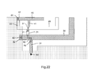
Fig.22 is a schematic view of a second embodiment of a three-band antenna according to the invention. - The exemplifications set out herein illustrate preferred embodiments of the invention, and such exemplifications are not to be construed as limiting the scope of the invention in any manner.
- As mentioned above, the invention relates to an antenna comprising a plurality of PIFAs.
Fig.2 shows the design of a single PIFA. - This antenna is printed on a substrate having two conductive metal layers: a top layer (in hatched line) on which are printed a feed element F a radiating element R and a ground return element GR, and a bottom layer on which is printed a ground section or ground plane G.
- The radiating element R is basically made up of a rectangular line. It can be also meandered to reduce its length. The length L0 of this element is substantially equal to a quarter of the wavelength at the center frequency of the targeted bandwidth of the antenna.
- The radiating element R is open-ended at one end and short-circuited to the ground section G by means of the ground return element GR and via-holes H at the other end. The radiating element and the feed element are offset transversally from the ground section G.
- The radiating element R is fed by the feed element F which is arranged perpendicularly to the radiating element, both elements together with the ground return element GR form with the vertical edge of the ground plane a kind of inverted-F shape. In this technical field, a PIFA designates an antenna having an inverted F shape or an antenna having a T shape.
- Several parameters are adjusted to achieve targeted performances of the antenna:
- the gap d1 between the feed element L and the vertical edge of the ground section G, the feed element width W0 and the gap d2 between the radiating element R and the horizontal edge of the ground plane are defined to match the antenna to the targeted impedance, meeting the requested return loss level.
- the length L0 and the width W0 of the radiating element R and the gap d3 between the end E1 of the radiating element and the right vertical edge of the ground section are defined to achieve the targeted bandwidth and the radiation performances (efficiency, gain).
- According to the invention, it is proposed a multi-band antenna based on a plurality of PIFAs which are stacked above each other.
- It is first described the invention in the case of a dual-band application.
Figures 3 to 6 illustrate a first embodiment of a dual-band antenna according to the invention. - As for the single PIFA, the dual band antenna is made on a substrate having two conductive metal layers: a top layer (in hatched line) attached to the top surface of the substrate and a bottom layer attached to the bottom layer of the substrate. The bottom layer comprises a
ground section 10. - A radiating
element 30, afeed element 31 and aground return element 32 are printed in the top layer. The radiatingelement 30 and thefeed element 31 are offset transversally from theground section 10. The radiatingelement 30 has an end connected to theground section 10 by means of theground return element 32 and via-holes 60. The other end of the radiatingelement 30 is open-ended. Thefeed element 31 is connected perpendicularly to the radiatingelement 30. The free end of thefeed element 31 is connected to afeed port 80. - In this embodiment, the radiating
element 30 comprises two successive rectangular portions, afirst portion 30A and asecond portion 30B which is perpendicular to theportion 30A. - The radiating
element 30, thefeed element 31 and theground return element 32 are arranged such that they form substantially a first printed inverted F antenna resonating in a first frequency band B1. The length L30 of the radiatingelement 30 is substantially equal to λ1/4, where λ1 is the wavelength at the center frequency of the band B1. - According to the invention, the bottom layer comprises also a radiating
element 20, afeed element 21 and aground return element 22. Theground return element 22 is part of theground section 10. Theground section 10 is shown in the figures by dots (area with dots). The radiatingelement 20 and thefeed element 21 are offset transversally from the radiatingelement 30 and thefeed element 31 of the top layer. - In this embodiment, the
feed elements microstrip line 50 printed in the bottom layer and via-holes 70. So, the twofeed elements feed port 80. - According to the invention, the radiating
element 20, thefeed element 21 and theground return element 22 are arranged such that they form substantially a second printed inverted F antenna resonating in a second frequency band B2. The length L20 of the radiatingelement 20 is substantially equal to λ2/4, where λ2 is the wavelength at the center frequency of the band B2. - This specific arrangement results in two cascaded PIFAs, the functionality of which can be relatively independent. It means that each PIFA can be optimized quite independently to the other. The parameters of PIFA resonating in the frequency band B1 can be adjusted by acting on the following values:
- the width W30 and the length L30 of the radiating
element 30, - the width W31 of the
feed element 31; - the distance d11 between a first vertical edge of the
ground section 10 and thefeed element 31; this distance is visible onFig.6 ; - the distance d12 between a horizontal edge of the
ground section 10 and theportion 30A of the radiatingelement 30; this distance is visible onFig.6 ; and - the distance d13 between a second vertical edge of the
ground section 10 and theportion 30B of the radiatingelement 30; this distance is visible onFig.6 . - In the same way, the parameters of PIFA resonating in the frequency band B2 can be adjusted by acting on the following values:
- the width W20 and the length L20 of the radiating
element 20, - the width W21 of the
feed element 21 - the width W50 of the
microstrip line 50; - the distance d21 between the first vertical edge of the
ground section 10 and thefeed element 21; this distance is visible onFig.6 ; - the distance d22 between the radiating
element 20 and theportion 30A of the radiatingelement 30; this distance is visible onFig.6 ; and - the distance d23 between the open end of the radiating
element 20 and theportion 30B of the radiatingelement 30; this distance is visible onFig.6 . - In the present embodiment, the length L30 of the PIFA resonating in the frequency B1 is higher than the length L20 of the PIFA resonating in the frequency B2 such that the band B1 is lower than the band B2.
- In this embodiment, the PIFA constituted by the radiating
element 30, thefeed element 31 and theground return element 32 forms the lower band PIFA and the PIFA constituted by the radiatingelement 20, thefeed element 21 and theground return element 22 forms the higher band PIFA. - The width W33, the distance d11 and the length L31 of the
feed element 31 are defined to match the impedance of the PIFA resonating in frequency Band B1 with the impedance of a radio frequency circuit connected to the feed port. - The width W31 and the length L31 of the
feed element 31 together with the width W21 and the length L21 of thefeed element 21, the width W50 of themicrostrip line 50 and the distance d21 are defined to match the impedance of the PIFA resonating in frequency Band B2 with the impedance of a radio frequency circuit connected to the feed port. - In a preferred embodiment illustrated by
Fig.7 , thefeed port 80 is connected to the radio frequency circuit via aninductor 26 cascaded in series with acapacitor 27, the inductance of theinductor 26 being determined in order to achieve impedance matching of the PIFA resonating in the higher band (band B2) with the radio frequency circuit and the capacitance of thecapacitor 27 being determined in order to achieve impedance matching of the PIFA resonating in the lower band (band B1) with the radio frequency circuit. - Variants of the first embodiment are illustrated by
Figs.8 to 10 . - In a variant shown at
Fig.8 , the radiatingelement 30 comprises a thirdstraight portion 30C connected perpendicularly to thecentral portion 30A at the opposite of theportion 30B, theportions - As a variant, the radiating
element 30 comprises a plurality of straight portions forming meanders. - In another variant illustrated by
Fig.9 , the radiatingelement 30 comprises a single straight portion. - In another variant illustrated by
Fig.10 , aslot 11 is etched in the bottom layer in order to achieve for instance a narrower bandwidth in the higher frequency band. - This dual-band antenna can be for example a WLAN dual-band 2.4/5GHz antenna. This antenna is for example printed onto a FR-4 substrate, the thickness of which is 1.2mm. In this case, it is possible to achieve a dual-band PIFA size of 22 x 8 mm2 onto PCB size of 240x142 mm2.
- The performances of such an antenna have been simulated by the HFSS™ 3D-EM simulation tool and are presented below. The simulated dual-band antenna comprises, at its input, an
inductor 26 of 2.5 nH cascaded with acapacitor 27 of 0.7 pF. - The performances of this antenna are illustrated by
Figs.11 to 19 .Fig.11 shows that the return loss levels are lower than the commonly required level (-10dB), in both bands [2.4GHz-2.5GHz] and [5.15 GHz-5.85GHz]. -
Fig.12 and Fig.13 show that the simulated gain is at a fair level, at around 4dBi and 5dBi in the 2.4 GHz and 5GHz bands respectively. -
Fig.14 and Fig.15 show that the antenna exhibits a high efficiency in both frequency bands, around 80-85%. -
Fig.16 andFig.17 show the 3D radiation patterns at 2.45 GHz and 5.5 GHz respectively. They are similar to what can exhibit a single band PIFA, with a radiation directed mainly to the front-side. -
Fig.18 andFig.19 show of the current distributions at 2.45 GHz and 5.5 GHz respectively.Fig.18 points out that the radiatingelement 20, which resonates in the higher band, is not very activated, demonstrating by this way that this element is quite transparent in the 2.4GHz band. When exciting the antenna in the higher band at 5.5GHz,Fig.19 shows that the radiatingelement 20 is resonating while the radiatingelement 30 drives the residual current, as also the ground plane surrounding it. - This topology of cascaded PIFAs can be extended to a multi-band antenna having more than two frequency bands. For example, it can be used for designing a 3-band antenna as illustrated by
Figs.20 and 21 . - The antenna of
Figs.20 and 21 comprises a multi-layered substrate and three superimposed conductive layers, each one of these conductive layers being separated from an adjacent conductive layer by a substrate layer. These conductive layers are defined as bottom layer, intermediate layer and top layer. The bottom layer comprises theground section 10. - Compared to the dual-band antenna of
Fig.3 , the antenna ofFigs.20 and 21 comprises an additional PIFA resonating in a frequency band B3 different from B1 and B2 printed in the intermediate layer. - So the top layer comprises a first PIFA made of the radiating
element 30, thefeed element 31 and theground return element 32. The bottom layer comprises a second PIFA made of the radiatingelement 20, thefeed element 21 and theground return element 22. And the intermediate layer comprises a third PIFA made of a radiatingelement 40, afeed element 41 and aground return element 42. - As for the dual-band antenna of
Fig.3 , the radiatingelement 30 is connected to theground section 10 by means of theground return element 32 and the via-holes 60. The radiatingelement 40 is connected toground section 10 by means of theground return element 42 and the via-holes 61. Theground return element 22 is connected to theground return 42 by said via-holes 61. - The
feed element 21 is connected to thefeed element 41 by means of amicrostrip line 50a printed in the bottom layer and via-holes 70a and thefeed element 41 is connected to thefeed element 31 by means of amicrostrip line 50b printed in the intermediate layer and via-holes 70b. - In this embodiment, as the length of the radiating
element 20 is lower than the length of the radiatingelement 40 which is itself lower than the length of the radiatingelement 30, the radiatingelement 30 resonates in a lower frequency band, the radiatingelement 40 resonates in an intermediate frequency band and the radiatingelement 20 resonates in a higher frequency band. - This topology of cascaded PIFAs can be extended to n-band antennas. In this embodiment, each conductive layer comprises a single PIFA. In a variant of 3-band antenna illustrated by
Fig.22 , one of the conductive layers comprises two PIFAs. The 3-band antenna comprises only two conductive layers, a bottom layer and a top layer. The PIFA made of the radiatingelement 20, thefeed element 21 and theground return element 22 is printed in the bottom layer and the two other PIFAs made of the radiatingelements feed elements ground return elements - As for the three-band antenna of
Fig.20 , the radiatingelement 30 is connected to theground section 10 by means of theground return element 32 and the via-holes 60. The radiatingelement 40 is connected toground section 10 by means of theground return element 42 and the via-holes 61. These elements are made in the top layer. - The radiating
element 20, thefeed element 21 and theground return element 22 made in the bottom layer are placed between the radiatingelement 40 and the radiatingelement 30. - The
ground return element 22 is directly connected to theground section 10. - The
feed element 41 is connected to thefeed element 21 by means of amicrostrip line 51 printed in the top layer and via-holes 71 and thefeed element 21 is connected to thefeed element 31 by means of amicrostrip line 50 printed in the bottom layer and via-holes 70. - This topology of multi-band antenna presents the following advantages:
- Its compactness that enables to reduce the surface area occupied by the numerous antennas in the PCB;
- size reduction enables to reduce the PCB cost.
- despite its compactness, the achieved performances are comparable to multi-single antenna performances; and
- it is an easy way to optimize the design to achieve the targeted performance that enables to reduce the time to market.
- While this invention has been described as having a preferred design, the present invention can be further modified within the scope of this disclosure. This application is therefore intended to cover any variations, uses, or adaptations of the invention using its general principles.
Claims (14)
- A multi-band antenna comprising- a substrate;- a first conductive layer and a second conductive layer separated from each other by said substrate, said second conductive layer comprising a ground section (10) and said first conductive layer comprising a first radiating element (30), a first feed element (31) connected to said first radiating element and a first ground return element (32) connected to said first radiating element and said ground section, said first radiating element (30) and said first feed element (31) being offset transversally from the ground section,
said first radiating element (30), said first feed element (31) and said first ground return element (32) being arranged in order to form substantially a first printed inverted F antenna resonating in a first frequency band,
characterized in that the second conductive layer further comprises a second radiating element (20), a second feed element (21) connected to said second radiating element and a second ground return element (22) connected to said second radiating element (20) and said first ground return element (32), said second ground return element (22) being part of said ground section (10), the length (L20) of the second radiating element being different from the length (L30) of the first radiating element, said second radiating element (20) and said second feed element (21) being offset transversally from said first radiating element (30) and said first feed element (31),
and in that said second radiating element (20), said second feed element (21) and said second ground return element (22) are arranged in order to form substantially a second printed inverted F antenna resonating in a second frequency band. - The multi-band antenna according to claim 1, wherein the first feed element (31) and the second feed element (21) are connected to a feed port (80).
- The multi-band antenna according to claim 2, wherein the second feed element (21) is connected to the first feed element (31) by a microstrip line (50) printed in the second conductive layer and via-holes (70), said microstrip line being arranged below or above the first radiating element.
- The multi-band antenna according to any one of preceding claims, wherein the first ground return element (32) is connected to the ground section (10) by via holes (60).
- The multi-band antenna according to claim 4, wherein the second ground return element (22) is connected to the first ground return element (32) by said via holes (60).
- The multi-band antenna according to any one of preceding claims, wherein the first radiating element (30) is a straight conductive line.
- The multi-band antenna according to any one of preceding claims, wherein the first radiating element comprises first and second successive straight portions (30B,30A), the second portion (30A) being perpendicular to the first portion (30B).
- The multi-band antenna according to any one of preceding claims, wherein the length (L30) of the first radiating element (30) is higher than the length (L20) of the second radiating element (20) such that the second frequency band is higher than the first frequency band.
- The multi-band antenna according to any one of preceding claims, wherein the length (L31) and the width (W31) of the first feed element (31) are defined to match the impedance of the first printed inverted F antenna with the impedance of a radio frequency circuit connected to the first feed element.
- The multi-band antenna according to claim 9, wherein the first feed element (31) is connected to the radio frequency circuit via an inductor (26) cascaded with a capacitor (27), the inductance of the inductor being determined in order to achieve impedance matching of the second printed inverted F antenna with the radio frequency circuit and the capacitance of the capacitor being determined in order to achieve impedance matching of the first printed inverted F antenna with the radio frequency circuit.
- The multi-band antenna according to claim 1, wherein it further comprises a third conductive layer of the substrate arranged between first and second conductive layers, said third conductive layer comprising a third radiating element (40), a third feed element (41) connected to said third radiating element and a third ground return element (42) connected to said third radiating element (40) and said ground section (10), the length (L40) of the third radiating element being different from the lengths (L30,L20) of said first and second radiating elements, said third radiating element (40) and said third feed element (41) being offset transversally from said first and second radiating elements (30,20), said first and second feed elements (31,21) and said ground section (10), and
said third radiating element (40), said third feed element (41) and said third ground return element (42) being arranged in order to form substantially a third printed inverted F antenna resonating in a third frequency band. - The multi-band antenna according to claim 11, wherein the first feed element (31), the second feed element (21) and the third feed element (41) are connected to a feed port (80).
- The multi-band antenna according to claim 12, wherein the second feed element (21) is connected to the third feed element (41) by a first microstrip line (50a) printed in the second conductive layer and via-holes (70a), said first microstrip line being arranged below or above the third radiating element (40), and the first feed element (31) is connected to the third feed element (41) by a second microstrip line (50b) printed in the third conductive layer and via-holes (70b), said second microstrip line being arranged below or above the first radiating element (30).
- The multi-band antenna according to claim 1, wherein one of said first and second conductive layers further comprises a third radiating element (40), a third feed element (41) connected to said third radiating element and a third ground return element (42) connected to said third radiating element (40) and said ground section (10), the length (L40) of the third radiating element being different from the lengths (L30,L20) of said first and second radiating elements, said third radiating element (40) and said third feed element (41) being offset transversally from said first and second radiating elements (30,20), said first and second feed elements (31,21) and said ground section (10),
said third radiating element (40), said third feed element (41) and said third ground return element (42) being arranged in order to form substantially a third printed inverted F antenna resonating in a third frequency band.
Priority Applications (8)
| Application Number | Priority Date | Filing Date | Title |
|---|---|---|---|
| EP13305482.5A EP2790268A1 (en) | 2013-04-12 | 2013-04-12 | Multi-band antenna |
| US14/880,710 US9711857B2 (en) | 2013-04-12 | 2014-04-10 | Multi-band antenna |
| EP14716822.3A EP2984703A1 (en) | 2013-04-12 | 2014-04-10 | Multi-band antenna |
| PCT/EP2014/057315 WO2014167072A1 (en) | 2013-04-12 | 2014-04-10 | Multi-band antenna |
| CN201480020697.7A CN105122541A (en) | 2013-04-12 | 2014-04-10 | Multi-band antenna |
| KR1020157032100A KR20150140796A (en) | 2013-04-12 | 2014-04-10 | Multi-band antenna |
| JP2016506977A JP2016514933A (en) | 2013-04-12 | 2014-04-10 | Multiband antenna |
| TW103113319A TW201445809A (en) | 2013-04-12 | 2014-04-11 | Multi-band antenna |
Applications Claiming Priority (1)
| Application Number | Priority Date | Filing Date | Title |
|---|---|---|---|
| EP13305482.5A EP2790268A1 (en) | 2013-04-12 | 2013-04-12 | Multi-band antenna |
Publications (1)
| Publication Number | Publication Date |
|---|---|
| EP2790268A1 true EP2790268A1 (en) | 2014-10-15 |
Family
ID=48236824
Family Applications (2)
| Application Number | Title | Priority Date | Filing Date |
|---|---|---|---|
| EP13305482.5A Withdrawn EP2790268A1 (en) | 2013-04-12 | 2013-04-12 | Multi-band antenna |
| EP14716822.3A Withdrawn EP2984703A1 (en) | 2013-04-12 | 2014-04-10 | Multi-band antenna |
Family Applications After (1)
| Application Number | Title | Priority Date | Filing Date |
|---|---|---|---|
| EP14716822.3A Withdrawn EP2984703A1 (en) | 2013-04-12 | 2014-04-10 | Multi-band antenna |
Country Status (7)
| Country | Link |
|---|---|
| US (1) | US9711857B2 (en) |
| EP (2) | EP2790268A1 (en) |
| JP (1) | JP2016514933A (en) |
| KR (1) | KR20150140796A (en) |
| CN (1) | CN105122541A (en) |
| TW (1) | TW201445809A (en) |
| WO (1) | WO2014167072A1 (en) |
Cited By (2)
| Publication number | Priority date | Publication date | Assignee | Title |
|---|---|---|---|---|
| WO2017184051A1 (en) | 2016-04-18 | 2017-10-26 | Incoax Networks Europe Ab | A multi-band wlan antenna device |
| EP3244486A1 (en) | 2016-05-09 | 2017-11-15 | Thomson Licensing | Antenna device for the coexistence of wireless systems |
Families Citing this family (23)
| Publication number | Priority date | Publication date | Assignee | Title |
|---|---|---|---|---|
| KR20160045312A (en) * | 2014-10-17 | 2016-04-27 | 삼성전자주식회사 | Antenna device and electronic device including the same |
| CN107785650B (en) * | 2016-08-31 | 2020-05-15 | 深圳富泰宏精密工业有限公司 | Antenna structure |
| EP3293823A1 (en) * | 2016-09-09 | 2018-03-14 | Thomson Licensing | Antenna feeder configured for feeding an antenna integrated within an electronic device |
| SG10201609104UA (en) * | 2016-10-31 | 2018-05-30 | Delta Electronics Inc | Dual-band dual-port antenna structure |
| DK3343782T3 (en) * | 2016-12-29 | 2019-10-28 | Oticon As | WIRELESS COMMUNICATION DEVICE TO COMMUNICATE WITH MULTIPLE EXTERNAL DEVICES THROUGH A WIRELESS COMMUNICATION DEVICE |
| TWI618296B (en) * | 2017-03-15 | 2018-03-11 | 智易科技股份有限公司 | Antenna structure |
| CN110870132B (en) * | 2017-08-04 | 2021-09-07 | 华为技术有限公司 | Multiband Antenna |
| CN107394384B (en) * | 2017-08-09 | 2023-10-13 | 歌尔科技有限公司 | Printed slot inverted F antenna and Bluetooth communication device |
| JP6678721B1 (en) | 2018-10-31 | 2020-04-08 | 京セラ株式会社 | Antenna, wireless communication module and wireless communication device |
| JP6678723B1 (en) | 2018-10-31 | 2020-04-08 | 京セラ株式会社 | Antenna, wireless communication module and wireless communication device |
| JP6678722B1 (en) | 2018-10-31 | 2020-04-08 | 京セラ株式会社 | Antenna, wireless communication module and wireless communication device |
| JP6814254B2 (en) * | 2019-06-27 | 2021-01-13 | 日本航空電子工業株式会社 | antenna |
| US10944153B1 (en) | 2019-08-29 | 2021-03-09 | Apple Inc. | Electronic devices having multi-band antenna structures |
| TWI734371B (en) * | 2020-02-07 | 2021-07-21 | 啓碁科技股份有限公司 | Antenna structure |
| CN111430897A (en) * | 2020-03-05 | 2020-07-17 | 泰凌微电子(上海)有限公司 | Antenna structure, communication device and method for forming antenna structure |
| CN111430900A (en) * | 2020-04-30 | 2020-07-17 | 曲龙跃 | All-printed ground radiation antenna system |
| CN111916885A (en) * | 2020-06-15 | 2020-11-10 | 上海创功通讯技术有限公司 | Dual-frenquency WIFI PCB antenna and terminal equipment |
| CN115441168A (en) * | 2022-08-09 | 2022-12-06 | 深圳市飞比电子科技有限公司 | Dual-band antenna device and ZigBee module |
| KR102624038B1 (en) * | 2022-10-27 | 2024-01-11 | 주식회사 오성전자 | PIFA type antenna |
| US12431621B2 (en) * | 2023-01-26 | 2025-09-30 | Honeywell International Inc. | Compact dual band antenna |
| CN118487027A (en) * | 2023-02-10 | 2024-08-13 | 台达电子工业股份有限公司 | Antenna structure and antenna device |
| US20250030273A1 (en) * | 2023-07-21 | 2025-01-23 | Southern Methodist University | Device for wireless power transfer |
| CN117240327B (en) * | 2023-11-13 | 2024-01-30 | 上海安其威微电子科技有限公司 | Non-contact connector |
Citations (5)
| Publication number | Priority date | Publication date | Assignee | Title |
|---|---|---|---|---|
| US20070096992A1 (en) * | 2005-10-28 | 2007-05-03 | Shinko Electric Industries Co. Ltd. | Antenna and wiring board |
| US20070182636A1 (en) * | 2006-02-06 | 2007-08-09 | Nokia Corporation | Dual band trace antenna for WLAN frequencies in a mobile phone |
| EP1848061A2 (en) * | 2006-04-19 | 2007-10-24 | Yokowo Co., Ltd. | Multi-band antenna |
| EP1860732A1 (en) * | 2005-03-15 | 2007-11-28 | Matsushita Electric Industrial Co., Ltd. | Antenna assembly and radio communication apparatus employing same |
| US20090278755A1 (en) * | 2008-05-12 | 2009-11-12 | Sony Ericsson Mobile Communications Japan, Inc. | Antenna device and communication terminal |
Family Cites Families (11)
| Publication number | Priority date | Publication date | Assignee | Title |
|---|---|---|---|---|
| US6670925B2 (en) * | 2001-06-01 | 2003-12-30 | Matsushita Electric Industrial Co., Ltd. | Inverted F-type antenna apparatus and portable radio communication apparatus provided with the inverted F-type antenna apparatus |
| DE10319093B3 (en) * | 2003-04-28 | 2004-11-04 | Fraunhofer-Gesellschaft zur Förderung der angewandten Forschung e.V. | antenna device |
| US7057560B2 (en) | 2003-05-07 | 2006-06-06 | Agere Systems Inc. | Dual-band antenna for a wireless local area network device |
| US6985114B2 (en) | 2003-06-09 | 2006-01-10 | Houkou Electric Co., Ltd. | Multi-frequency antenna and constituting method thereof |
| US7274334B2 (en) * | 2005-03-24 | 2007-09-25 | Tdk Corporation | Stacked multi-resonator antenna |
| US7324054B2 (en) | 2005-09-29 | 2008-01-29 | Sony Ericsson Mobile Communications Ab | Multi-band PIFA |
| US7280074B1 (en) | 2006-03-30 | 2007-10-09 | Delta Networks, Inc. | Multiple frequency band planar antenna |
| WO2011163139A1 (en) * | 2010-06-21 | 2011-12-29 | Rftelligent, Inc. | Wideband printed circuit board-printed antenna for radio frequency front end circuit |
| CN201845856U (en) | 2010-08-23 | 2011-05-25 | 中兴通讯股份有限公司 | Multi-band mobile terminal antenna |
| TWI459638B (en) * | 2011-08-02 | 2014-11-01 | Quanta Comp Inc | An antenna combination that reduces the specific absorption ratio of electromagnetic waves |
| TWI539676B (en) * | 2013-09-03 | 2016-06-21 | 宏碁股份有限公司 | Communication device |
-
2013
- 2013-04-12 EP EP13305482.5A patent/EP2790268A1/en not_active Withdrawn
-
2014
- 2014-04-10 US US14/880,710 patent/US9711857B2/en not_active Expired - Fee Related
- 2014-04-10 JP JP2016506977A patent/JP2016514933A/en active Pending
- 2014-04-10 WO PCT/EP2014/057315 patent/WO2014167072A1/en not_active Ceased
- 2014-04-10 KR KR1020157032100A patent/KR20150140796A/en not_active Withdrawn
- 2014-04-10 CN CN201480020697.7A patent/CN105122541A/en active Pending
- 2014-04-10 EP EP14716822.3A patent/EP2984703A1/en not_active Withdrawn
- 2014-04-11 TW TW103113319A patent/TW201445809A/en unknown
Patent Citations (5)
| Publication number | Priority date | Publication date | Assignee | Title |
|---|---|---|---|---|
| EP1860732A1 (en) * | 2005-03-15 | 2007-11-28 | Matsushita Electric Industrial Co., Ltd. | Antenna assembly and radio communication apparatus employing same |
| US20070096992A1 (en) * | 2005-10-28 | 2007-05-03 | Shinko Electric Industries Co. Ltd. | Antenna and wiring board |
| US20070182636A1 (en) * | 2006-02-06 | 2007-08-09 | Nokia Corporation | Dual band trace antenna for WLAN frequencies in a mobile phone |
| EP1848061A2 (en) * | 2006-04-19 | 2007-10-24 | Yokowo Co., Ltd. | Multi-band antenna |
| US20090278755A1 (en) * | 2008-05-12 | 2009-11-12 | Sony Ericsson Mobile Communications Japan, Inc. | Antenna device and communication terminal |
Cited By (5)
| Publication number | Priority date | Publication date | Assignee | Title |
|---|---|---|---|---|
| WO2017184051A1 (en) | 2016-04-18 | 2017-10-26 | Incoax Networks Europe Ab | A multi-band wlan antenna device |
| EP3446360A4 (en) * | 2016-04-18 | 2019-05-01 | InCoax Networks AB | A multi-band wlan antenna device |
| US10283840B2 (en) | 2016-04-18 | 2019-05-07 | Incoax Networks Ab | Multi-band WLAN antenna device |
| EP3244486A1 (en) | 2016-05-09 | 2017-11-15 | Thomson Licensing | Antenna device for the coexistence of wireless systems |
| WO2017194325A1 (en) | 2016-05-09 | 2017-11-16 | Thomson Licensing | Antenna device for the coexistence of wireless systems |
Also Published As
| Publication number | Publication date |
|---|---|
| US20160294062A1 (en) | 2016-10-06 |
| CN105122541A (en) | 2015-12-02 |
| JP2016514933A (en) | 2016-05-23 |
| KR20150140796A (en) | 2015-12-16 |
| WO2014167072A1 (en) | 2014-10-16 |
| EP2984703A1 (en) | 2016-02-17 |
| US9711857B2 (en) | 2017-07-18 |
| TW201445809A (en) | 2014-12-01 |
Similar Documents
| Publication | Publication Date | Title |
|---|---|---|
| US9711857B2 (en) | Multi-band antenna | |
| US7663551B2 (en) | Multiband antenna apparatus and methods | |
| KR101837225B1 (en) | A loop antenna for mobile handset and other applications | |
| US8976070B2 (en) | Broadcasting antenna for vehicle and shark fin antenna apparatus having the same | |
| US10522909B2 (en) | Multi-input multi-output antenna | |
| CN106532259B (en) | Antenna system and antenna module with reduced interference between radiation patterns | |
| EP3649697B1 (en) | Modular multi-stage antenna system and component for wireless communications | |
| KR101622170B1 (en) | External antenna for vehicle | |
| JP4858860B2 (en) | Multiband antenna | |
| US20100149057A9 (en) | Multiband antenna system and methods | |
| CN103151601A (en) | Bottom edge slot coupled antenna | |
| CN109075436A (en) | Ultra wideband dual polarization radiating element for antenna for base station | |
| JP2017511667A (en) | Antenna system using capacitively coupled loop antenna with provision of antenna isolation | |
| JP2005510927A (en) | Dual band antenna device | |
| JP3898710B2 (en) | Multi-band multilayer chip antenna using double coupling feed | |
| US9954285B2 (en) | WiFi patch antenna with dual u-shaped slots | |
| US10777896B2 (en) | Coupled antenna system for multiband operation | |
| JP2017530614A (en) | Decoupling antenna for wireless communication | |
| KR100972846B1 (en) | Multiband Antennas for Mobile Devices | |
| JP6624650B2 (en) | antenna | |
| EP3154125B1 (en) | Eight-frequency band antenna | |
| CN107112634A (en) | Antenna assembly and communicator | |
| KR20090076197A (en) | Multiband Chip Antenna of Mobile Communication Terminal | |
| WO2019008171A1 (en) | Modular multi-stage antenna system and component for wireless communications | |
| US20050285802A1 (en) | Dual-band antenna |
Legal Events
| Date | Code | Title | Description |
|---|---|---|---|
| PUAI | Public reference made under article 153(3) epc to a published international application that has entered the european phase |
Free format text: ORIGINAL CODE: 0009012 |
|
| 17P | Request for examination filed |
Effective date: 20130412 |
|
| AK | Designated contracting states |
Kind code of ref document: A1 Designated state(s): AL AT BE BG CH CY CZ DE DK EE ES FI FR GB GR HR HU IE IS IT LI LT LU LV MC MK MT NL NO PL PT RO RS SE SI SK SM TR |
|
| AX | Request for extension of the european patent |
Extension state: BA ME |
|
| STAA | Information on the status of an ep patent application or granted ep patent |
Free format text: STATUS: THE APPLICATION IS DEEMED TO BE WITHDRAWN |
|
| 18D | Application deemed to be withdrawn |
Effective date: 20150416 |