EP2789712A1 - Method of making a multicomponent film - Google Patents
Method of making a multicomponent film Download PDFInfo
- Publication number
- EP2789712A1 EP2789712A1 EP20140164386 EP14164386A EP2789712A1 EP 2789712 A1 EP2789712 A1 EP 2789712A1 EP 20140164386 EP20140164386 EP 20140164386 EP 14164386 A EP14164386 A EP 14164386A EP 2789712 A1 EP2789712 A1 EP 2789712A1
- Authority
- EP
- European Patent Office
- Prior art keywords
- precursor
- film
- introducing
- germanium
- substrate
- Prior art date
- Legal status (The legal status is an assumption and is not a legal conclusion. Google has not performed a legal analysis and makes no representation as to the accuracy of the status listed.)
- Granted
Links
Images



Classifications
-
- C—CHEMISTRY; METALLURGY
- C23—COATING METALLIC MATERIAL; COATING MATERIAL WITH METALLIC MATERIAL; CHEMICAL SURFACE TREATMENT; DIFFUSION TREATMENT OF METALLIC MATERIAL; COATING BY VACUUM EVAPORATION, BY SPUTTERING, BY ION IMPLANTATION OR BY CHEMICAL VAPOUR DEPOSITION, IN GENERAL; INHIBITING CORROSION OF METALLIC MATERIAL OR INCRUSTATION IN GENERAL
- C23C—COATING METALLIC MATERIAL; COATING MATERIAL WITH METALLIC MATERIAL; SURFACE TREATMENT OF METALLIC MATERIAL BY DIFFUSION INTO THE SURFACE, BY CHEMICAL CONVERSION OR SUBSTITUTION; COATING BY VACUUM EVAPORATION, BY SPUTTERING, BY ION IMPLANTATION OR BY CHEMICAL VAPOUR DEPOSITION, IN GENERAL
- C23C16/00—Chemical coating by decomposition of gaseous compounds, without leaving reaction products of surface material in the coating, i.e. chemical vapour deposition [CVD] processes
- C23C16/44—Chemical coating by decomposition of gaseous compounds, without leaving reaction products of surface material in the coating, i.e. chemical vapour deposition [CVD] processes characterised by the method of coating
- C23C16/455—Chemical coating by decomposition of gaseous compounds, without leaving reaction products of surface material in the coating, i.e. chemical vapour deposition [CVD] processes characterised by the method of coating characterised by the method used for introducing gases into reaction chamber or for modifying gas flows in reaction chamber
- C23C16/45523—Pulsed gas flow or change of composition over time
- C23C16/45525—Atomic layer deposition [ALD]
- C23C16/45527—Atomic layer deposition [ALD] characterized by the ALD cycle, e.g. different flows or temperatures during half-reactions, unusual pulsing sequence, use of precursor mixtures or auxiliary reactants or activations
- C23C16/45529—Atomic layer deposition [ALD] characterized by the ALD cycle, e.g. different flows or temperatures during half-reactions, unusual pulsing sequence, use of precursor mixtures or auxiliary reactants or activations specially adapted for making a layer stack of alternating different compositions or gradient compositions
-
- C—CHEMISTRY; METALLURGY
- C23—COATING METALLIC MATERIAL; COATING MATERIAL WITH METALLIC MATERIAL; CHEMICAL SURFACE TREATMENT; DIFFUSION TREATMENT OF METALLIC MATERIAL; COATING BY VACUUM EVAPORATION, BY SPUTTERING, BY ION IMPLANTATION OR BY CHEMICAL VAPOUR DEPOSITION, IN GENERAL; INHIBITING CORROSION OF METALLIC MATERIAL OR INCRUSTATION IN GENERAL
- C23C—COATING METALLIC MATERIAL; COATING MATERIAL WITH METALLIC MATERIAL; SURFACE TREATMENT OF METALLIC MATERIAL BY DIFFUSION INTO THE SURFACE, BY CHEMICAL CONVERSION OR SUBSTITUTION; COATING BY VACUUM EVAPORATION, BY SPUTTERING, BY ION IMPLANTATION OR BY CHEMICAL VAPOUR DEPOSITION, IN GENERAL
- C23C16/00—Chemical coating by decomposition of gaseous compounds, without leaving reaction products of surface material in the coating, i.e. chemical vapour deposition [CVD] processes
- C23C16/22—Chemical coating by decomposition of gaseous compounds, without leaving reaction products of surface material in the coating, i.e. chemical vapour deposition [CVD] processes characterised by the deposition of inorganic material, other than metallic material
-
- C—CHEMISTRY; METALLURGY
- C23—COATING METALLIC MATERIAL; COATING MATERIAL WITH METALLIC MATERIAL; CHEMICAL SURFACE TREATMENT; DIFFUSION TREATMENT OF METALLIC MATERIAL; COATING BY VACUUM EVAPORATION, BY SPUTTERING, BY ION IMPLANTATION OR BY CHEMICAL VAPOUR DEPOSITION, IN GENERAL; INHIBITING CORROSION OF METALLIC MATERIAL OR INCRUSTATION IN GENERAL
- C23C—COATING METALLIC MATERIAL; COATING MATERIAL WITH METALLIC MATERIAL; SURFACE TREATMENT OF METALLIC MATERIAL BY DIFFUSION INTO THE SURFACE, BY CHEMICAL CONVERSION OR SUBSTITUTION; COATING BY VACUUM EVAPORATION, BY SPUTTERING, BY ION IMPLANTATION OR BY CHEMICAL VAPOUR DEPOSITION, IN GENERAL
- C23C16/00—Chemical coating by decomposition of gaseous compounds, without leaving reaction products of surface material in the coating, i.e. chemical vapour deposition [CVD] processes
- C23C16/22—Chemical coating by decomposition of gaseous compounds, without leaving reaction products of surface material in the coating, i.e. chemical vapour deposition [CVD] processes characterised by the deposition of inorganic material, other than metallic material
- C23C16/28—Deposition of only one other non-metal element
-
- C—CHEMISTRY; METALLURGY
- C23—COATING METALLIC MATERIAL; COATING MATERIAL WITH METALLIC MATERIAL; CHEMICAL SURFACE TREATMENT; DIFFUSION TREATMENT OF METALLIC MATERIAL; COATING BY VACUUM EVAPORATION, BY SPUTTERING, BY ION IMPLANTATION OR BY CHEMICAL VAPOUR DEPOSITION, IN GENERAL; INHIBITING CORROSION OF METALLIC MATERIAL OR INCRUSTATION IN GENERAL
- C23C—COATING METALLIC MATERIAL; COATING MATERIAL WITH METALLIC MATERIAL; SURFACE TREATMENT OF METALLIC MATERIAL BY DIFFUSION INTO THE SURFACE, BY CHEMICAL CONVERSION OR SUBSTITUTION; COATING BY VACUUM EVAPORATION, BY SPUTTERING, BY ION IMPLANTATION OR BY CHEMICAL VAPOUR DEPOSITION, IN GENERAL
- C23C16/00—Chemical coating by decomposition of gaseous compounds, without leaving reaction products of surface material in the coating, i.e. chemical vapour deposition [CVD] processes
- C23C16/22—Chemical coating by decomposition of gaseous compounds, without leaving reaction products of surface material in the coating, i.e. chemical vapour deposition [CVD] processes characterised by the deposition of inorganic material, other than metallic material
- C23C16/30—Deposition of compounds, mixtures or solid solutions, e.g. borides, carbides, nitrides
- C23C16/305—Sulfides, selenides, or tellurides
-
- C—CHEMISTRY; METALLURGY
- C23—COATING METALLIC MATERIAL; COATING MATERIAL WITH METALLIC MATERIAL; CHEMICAL SURFACE TREATMENT; DIFFUSION TREATMENT OF METALLIC MATERIAL; COATING BY VACUUM EVAPORATION, BY SPUTTERING, BY ION IMPLANTATION OR BY CHEMICAL VAPOUR DEPOSITION, IN GENERAL; INHIBITING CORROSION OF METALLIC MATERIAL OR INCRUSTATION IN GENERAL
- C23C—COATING METALLIC MATERIAL; COATING MATERIAL WITH METALLIC MATERIAL; SURFACE TREATMENT OF METALLIC MATERIAL BY DIFFUSION INTO THE SURFACE, BY CHEMICAL CONVERSION OR SUBSTITUTION; COATING BY VACUUM EVAPORATION, BY SPUTTERING, BY ION IMPLANTATION OR BY CHEMICAL VAPOUR DEPOSITION, IN GENERAL
- C23C16/00—Chemical coating by decomposition of gaseous compounds, without leaving reaction products of surface material in the coating, i.e. chemical vapour deposition [CVD] processes
- C23C16/44—Chemical coating by decomposition of gaseous compounds, without leaving reaction products of surface material in the coating, i.e. chemical vapour deposition [CVD] processes characterised by the method of coating
- C23C16/455—Chemical coating by decomposition of gaseous compounds, without leaving reaction products of surface material in the coating, i.e. chemical vapour deposition [CVD] processes characterised by the method of coating characterised by the method used for introducing gases into reaction chamber or for modifying gas flows in reaction chamber
- C23C16/45523—Pulsed gas flow or change of composition over time
- C23C16/45525—Atomic layer deposition [ALD]
-
- C—CHEMISTRY; METALLURGY
- C23—COATING METALLIC MATERIAL; COATING MATERIAL WITH METALLIC MATERIAL; CHEMICAL SURFACE TREATMENT; DIFFUSION TREATMENT OF METALLIC MATERIAL; COATING BY VACUUM EVAPORATION, BY SPUTTERING, BY ION IMPLANTATION OR BY CHEMICAL VAPOUR DEPOSITION, IN GENERAL; INHIBITING CORROSION OF METALLIC MATERIAL OR INCRUSTATION IN GENERAL
- C23C—COATING METALLIC MATERIAL; COATING MATERIAL WITH METALLIC MATERIAL; SURFACE TREATMENT OF METALLIC MATERIAL BY DIFFUSION INTO THE SURFACE, BY CHEMICAL CONVERSION OR SUBSTITUTION; COATING BY VACUUM EVAPORATION, BY SPUTTERING, BY ION IMPLANTATION OR BY CHEMICAL VAPOUR DEPOSITION, IN GENERAL
- C23C16/00—Chemical coating by decomposition of gaseous compounds, without leaving reaction products of surface material in the coating, i.e. chemical vapour deposition [CVD] processes
- C23C16/44—Chemical coating by decomposition of gaseous compounds, without leaving reaction products of surface material in the coating, i.e. chemical vapour deposition [CVD] processes characterised by the method of coating
- C23C16/455—Chemical coating by decomposition of gaseous compounds, without leaving reaction products of surface material in the coating, i.e. chemical vapour deposition [CVD] processes characterised by the method of coating characterised by the method used for introducing gases into reaction chamber or for modifying gas flows in reaction chamber
- C23C16/45523—Pulsed gas flow or change of composition over time
- C23C16/45525—Atomic layer deposition [ALD]
- C23C16/45527—Atomic layer deposition [ALD] characterized by the ALD cycle, e.g. different flows or temperatures during half-reactions, unusual pulsing sequence, use of precursor mixtures or auxiliary reactants or activations
- C23C16/45531—Atomic layer deposition [ALD] characterized by the ALD cycle, e.g. different flows or temperatures during half-reactions, unusual pulsing sequence, use of precursor mixtures or auxiliary reactants or activations specially adapted for making ternary or higher compositions
-
- C—CHEMISTRY; METALLURGY
- C23—COATING METALLIC MATERIAL; COATING MATERIAL WITH METALLIC MATERIAL; CHEMICAL SURFACE TREATMENT; DIFFUSION TREATMENT OF METALLIC MATERIAL; COATING BY VACUUM EVAPORATION, BY SPUTTERING, BY ION IMPLANTATION OR BY CHEMICAL VAPOUR DEPOSITION, IN GENERAL; INHIBITING CORROSION OF METALLIC MATERIAL OR INCRUSTATION IN GENERAL
- C23C—COATING METALLIC MATERIAL; COATING MATERIAL WITH METALLIC MATERIAL; SURFACE TREATMENT OF METALLIC MATERIAL BY DIFFUSION INTO THE SURFACE, BY CHEMICAL CONVERSION OR SUBSTITUTION; COATING BY VACUUM EVAPORATION, BY SPUTTERING, BY ION IMPLANTATION OR BY CHEMICAL VAPOUR DEPOSITION, IN GENERAL
- C23C16/00—Chemical coating by decomposition of gaseous compounds, without leaving reaction products of surface material in the coating, i.e. chemical vapour deposition [CVD] processes
- C23C16/44—Chemical coating by decomposition of gaseous compounds, without leaving reaction products of surface material in the coating, i.e. chemical vapour deposition [CVD] processes characterised by the method of coating
- C23C16/455—Chemical coating by decomposition of gaseous compounds, without leaving reaction products of surface material in the coating, i.e. chemical vapour deposition [CVD] processes characterised by the method of coating characterised by the method used for introducing gases into reaction chamber or for modifying gas flows in reaction chamber
- C23C16/45523—Pulsed gas flow or change of composition over time
- C23C16/45525—Atomic layer deposition [ALD]
- C23C16/45527—Atomic layer deposition [ALD] characterized by the ALD cycle, e.g. different flows or temperatures during half-reactions, unusual pulsing sequence, use of precursor mixtures or auxiliary reactants or activations
- C23C16/45534—Use of auxiliary reactants other than used for contributing to the composition of the main film, e.g. catalysts, activators or scavengers
-
- C—CHEMISTRY; METALLURGY
- C23—COATING METALLIC MATERIAL; COATING MATERIAL WITH METALLIC MATERIAL; CHEMICAL SURFACE TREATMENT; DIFFUSION TREATMENT OF METALLIC MATERIAL; COATING BY VACUUM EVAPORATION, BY SPUTTERING, BY ION IMPLANTATION OR BY CHEMICAL VAPOUR DEPOSITION, IN GENERAL; INHIBITING CORROSION OF METALLIC MATERIAL OR INCRUSTATION IN GENERAL
- C23C—COATING METALLIC MATERIAL; COATING MATERIAL WITH METALLIC MATERIAL; SURFACE TREATMENT OF METALLIC MATERIAL BY DIFFUSION INTO THE SURFACE, BY CHEMICAL CONVERSION OR SUBSTITUTION; COATING BY VACUUM EVAPORATION, BY SPUTTERING, BY ION IMPLANTATION OR BY CHEMICAL VAPOUR DEPOSITION, IN GENERAL
- C23C16/00—Chemical coating by decomposition of gaseous compounds, without leaving reaction products of surface material in the coating, i.e. chemical vapour deposition [CVD] processes
- C23C16/44—Chemical coating by decomposition of gaseous compounds, without leaving reaction products of surface material in the coating, i.e. chemical vapour deposition [CVD] processes characterised by the method of coating
- C23C16/455—Chemical coating by decomposition of gaseous compounds, without leaving reaction products of surface material in the coating, i.e. chemical vapour deposition [CVD] processes characterised by the method of coating characterised by the method used for introducing gases into reaction chamber or for modifying gas flows in reaction chamber
- C23C16/45523—Pulsed gas flow or change of composition over time
- C23C16/45525—Atomic layer deposition [ALD]
- C23C16/45553—Atomic layer deposition [ALD] characterized by the use of precursors specially adapted for ALD
-
- H—ELECTRICITY
- H10—SEMICONDUCTOR DEVICES; ELECTRIC SOLID-STATE DEVICES NOT OTHERWISE PROVIDED FOR
- H10N—ELECTRIC SOLID-STATE DEVICES NOT OTHERWISE PROVIDED FOR
- H10N70/00—Solid-state devices having no potential barriers, and specially adapted for rectifying, amplifying, oscillating or switching
- H10N70/011—Manufacture or treatment of multistable switching devices
- H10N70/021—Formation of switching materials, e.g. deposition of layers
- H10N70/023—Formation of switching materials, e.g. deposition of layers by chemical vapor deposition, e.g. MOCVD, ALD
-
- H—ELECTRICITY
- H10—SEMICONDUCTOR DEVICES; ELECTRIC SOLID-STATE DEVICES NOT OTHERWISE PROVIDED FOR
- H10N—ELECTRIC SOLID-STATE DEVICES NOT OTHERWISE PROVIDED FOR
- H10N70/00—Solid-state devices having no potential barriers, and specially adapted for rectifying, amplifying, oscillating or switching
- H10N70/20—Multistable switching devices, e.g. memristors
- H10N70/231—Multistable switching devices, e.g. memristors based on solid-state phase change, e.g. between amorphous and crystalline phases, Ovshinsky effect
-
- H—ELECTRICITY
- H10—SEMICONDUCTOR DEVICES; ELECTRIC SOLID-STATE DEVICES NOT OTHERWISE PROVIDED FOR
- H10N—ELECTRIC SOLID-STATE DEVICES NOT OTHERWISE PROVIDED FOR
- H10N70/00—Solid-state devices having no potential barriers, and specially adapted for rectifying, amplifying, oscillating or switching
- H10N70/801—Constructional details of multistable switching devices
- H10N70/881—Switching materials
- H10N70/882—Compounds of sulfur, selenium or tellurium, e.g. chalcogenides
- H10N70/8828—Tellurides, e.g. GeSbTe
Definitions
- a method for depositing multicomponent films each of which may be stoichiometric or non-stoichiometric such as, but not limited to, Germanium Tellurium (GT), Antimony Germanium (SG), Germanium Antimony Tellurium (GST), Germanium Oxide, Germanium Nitride.
- GT Germanium Tellurium
- SG Antimony Germanium
- GST Germanium Antimony Tellurium
- Oxide Germanium Oxide
- Germanium Nitride Germanium Nitride
- Phase-change materials exist in a crystalline state or an amorphous state according to temperature.
- a phase-change material has a more ordered atomic arrangement and a lower electrical resistance in a crystalline state than in an amorphous state.
- a phase-change material can be reversibly transformed from the crystalline state to the amorphous state based on an operating temperature.
- Such characteristics that is, reversible phase change and different resistances of different states, are applied to newly proposed electronic devices, a new type of nonvolatile memory devices, phase-change random access memory (PCRAM) devices.
- the electrical resistance of a PCRAM may vary based on a state (e.g., crystalline, amorphous, etc.) of a phase-change material included therein.
- phase-change materials used for memory devices
- the most commonly used are ternary chalcogenides of Group 14 and Group 15 elements, such as Germanium Antimony Tellurium compounds of various compositions, including but not limited to Ge 2 Sb 2 Te 5 , and commonly abbreviated as GST.
- the solid phases of GST can rapidly change from crystalline state to amorphous state or vice versa upon heating and cooling cycles.
- the amorphous GST has relatively higher electrical resistance while the crystalline GST has relatively lower electrical resistance.
- PCRAM phase change random access memory
- ALD GeSbTe atomic layer deposition
- GST lie on the GeTe-Sb 2 Te 3 pseudo-binary tie line.
- ALD deposition of these compositions is difficult because of the greater stability of Ge +4 precursors than Ge +2 precursors and Ge +4 tends to form GeTe 2 instead of GeTe. Under these circumstances GeTe 2 -Sb 2 Te 3 composition films would be formed. Therefore, there is a need for precursors and related manufacturing methods or processes for forming GT and GST films which can produce films with high conformality and chemical composition uniformity, particularly using an ALD deposition process.
- HGeCl 3 trichlorogermane
- HGeCl 3 trichlorogermane
- HGeCl 3 can easily dissociate into HCl and GeCl 2 at relatively low temperature.
- This property makes HGeCl 3 a suitable precursor which can generate divalent germanium species in situ in the deposition process.
- HGeCl 3 when used in a deposition process with other precursors (Me 3 Si) 2 Te and (EtO) 3 Sb, may increase the germanium composition in GST alloy, comparing with commonly used Ge precursors such as (MeO) 4 Ge.
- the use of HGeCl 3 as an germanium precursor allows one to solve the aforementioned problems of other previous germanium precursors and achieve the desired Ge 2 Sb 2 Te 5 composition in certain embodiments.
- steps (a) through (f) are repeated a number of times until a desired thickness of coating layers is reached to provide the multicomponent film.
- the steps may be performed in the order of:
- a process of depositing a multicomponent film onto at least a portion of a substrate comprising the steps of:
- a process of depositing a germanium-containing film onto at least a portion of a substrate comprising the steps of: providing the substrate within a reactor; introducing into the reactor a Ge precursor comprising HGeCl 3 under deposition conditions sufficient to react with the substrate to provide a germanium-containing film.
- the introducing preferably further comprises an oxygen source or nitrogen source.
- Exemplary oxygen sources employed include, but are not limited to, oxygen (O 2 ), oxygen plasma, ozone (O 3 ), hydrogen peroxide, air, nitrous oxide, water plasma, and water.
- the germanium-containing film further comprises a nitrogen source to provide a germanium nitride (GeN or Ge 3 N 4 ) film.
- exemplary nitrogen sources include but are not limited to ammonia, ammonia plasma, nitrogen/hydrogen plasma, and nitrogen plasma.
- the germanium-containing film preferably comprises a pure germanium film via introducing hydrogen plasma.
- the germanium film preferably further comprises nitridation using nitrogen plasma or ammonia plasma or nitrogen/hydrogen plasma to convert into a germanium nitride film.
- Preferred substrates include silicon oxide and titanium nitride.
- the steps of the methods described herein may be performed in a variety of orders, may be performed sequentially or concurrently (e.g., during at least a portion of another step), and in any combination thereof. In certain embodiments, the steps described herein are performed sequentially to avoid formation of precipitates.
- Atomic Layer Deposition is a preferred technology to deposit films, such as metal chalcogenide films, uniformly on small dimensional structures on a substrate surface.
- the film comprises a metal chalcogenide film.
- metal chalcogenide refers to a film that contains one or more Group 16 ion (chalcogenide) and at least one electropositive element. Examples of chalcogenide materials include, but are not limited to, sulfides, selenides, and tellurides.
- Conventional ALD technology involves ALD reactors which typically operate under vacuum and at elevated temperature.
- ALD is a type of chemical vapor deposition that is used for highly controlled deposition of thin films. It is a self-limiting (e.g., the amount of film material deposited in each reaction cycle is constant) and sequential (e.g., the precursor vapors are brought onto the substrates alternately, one at a time, separated by purging periods with inert gas) process. ALD is considered a deposition method with the greatest potential for producing very thin, conformal films with control of the thickness and composition of the films possible at the atomic level. Using ALD, film thickness depends only on the number of reaction cycles, which makes the thickness control accurate and simple.
- Described herein are methods and precursors for depositing germanium-containing films are multi-component films such as without limitation GeTe and GeTeSb films.
- Exemplary depositions temperatures for the method described here include ranges having any one or more of the following endpoints: 500, 400, 300, 200, 195, 190, 185, 180, 175, 170, 165, 160, 155, 150, 145, 140, 135, 130, 125, 120, 115, 110, 105, 100, 95, 90, 85, 80, 75, 70, 65, 60, 55, 50, 45, 40, 35, 30, 25, and/or 20°C.
- Examples of particular temperature ranges include, but are not limited to, from about 20 to about 200°C or from about 50 to about 100°C.
- the germanium-containing films further comprise tellurium and are deposited using a tellurium precursor.
- exemplary tellurium precursors can be selected from disilyltellurium, silylalkyltellurium, silylaminotellurium with the general structures of: (R 1 R 2 R 3 Si) 2 Te (R 1 R 2 R 3 Si)TeR 4 (R 1 R 2 R 3 Si)TeN(R 4 R 5 ) where R 1 , R 2 , R 3 , R 4 , and R 5 are independently selected from hydrogen, an alkyl group having 1 - 10 carbons in linear, branched, or cyclic forms without or with double bonds, or a C 3 to C 10 aryl group.
- the tellurium precursors, alcohols, germanium and antimony precursors, such as (Me 2 N) 4 Ge and (Me 2 N) 3 Sb are suitably introduced to a deposition chamber in any sequence in a cyclic manner by vapor draw or direct liquid injection (DLI).
- the deposition temperature is preferably between 25° to 500° C.
- steps (a) through (f) are repeated a number of times until a desired thickness of coating layers is reached to provide the multicomponent film.
- the steps may be performed in the order of:
- the ALD cycle is repeated a certain number of times until the desired film thickness is achieved.
- the next ALD cycle starts with Steps a) to d) and the steps are repeated until the desired thickness of film is obtained.
- the method for depositing a multicomponent film onto at least a portion of a substrate comprises the steps:
- the ALD cycle is repeated a certain number of times until the desired film thickness is achieved.
- the next ALD cycle starts with Step a through Step h which cycle is then repeated until the desired thickness of film is obtained.
- the steps may be performed in the order of:
- the order of Steps a to h can be alternated to achieve required GST film such as ratio of Ge vs Sb or Ge vs Te.
- Exemplary silyltellurium compounds used in the process described herein have the following formulae: (R 1 R 2 R 3 Si) 2 Te; (R 1 R 2 R 3 Si)TeR 4 ; and (R 1 R 2 R 3 Si)TeN(R 4 R 5 ) where R 1 , R 2 , R 3 , R 4 and R 5 are each individually a hydrogen atom, an alkyl groups with 1 to 10 carbons in a linear, branched, or cyclic form, or aromatic groups with 4 to 10 carbons.
- Exemplary aminogermanes, aminoantimony, and antimony alkoxides in the process described herein have the following formulae: (R 1 R 2 N) 4 Ge (R 1 R 2 N) 3 Sb (R 1 O) 3 Sb where R 1 and R 2 are each individually alkyl groups with 1 to 10 carbons in linear, branched, or cyclic form.
- aryl denotes an aromatic cyclic or an aromatic heterocyclic group or an aralkyl group having from 4 to 10 carbon atoms, from 4 to 10, from 5 to 10 carbon atoms, or from 6 to 10 carbon atoms.
- exemplary aryl groups include, but are not limited to, pyrrolyl, phenyl, benzyl, chlorobenzyl, tolyl, and o-xylyl.
- the multicomponent film is deposited using an ALD method.
- the method described herein can be used to provide a thin film in a deposition apparatus.
- the deposition apparatus suitably consists of the following parts.
- the reactor is filled with inert gas (e.g., Ar or N 2 ) through an inlet and then pumped out using a vacuum pump 8 to a vacuum level below 20 mTorr (2.7 Pa).
- inert gas e.g., Ar or N 2
- the reactor is then filled with inlet gas again and the reactor wall and substrate holder are heated to a temperature between 25 °C to 500 °C at which the deposition is set to begin.
- the Ge precursor is delivered from a precursor container that is heated to a certain temperature range. The temperature remains constant during the deposition.
- the precursor is delivered from a precursor container that is heated to a temperature between 25 °C and 500 °C.
- the temperature also remains constant during the deposition.
- the number of the cycles is preset according to the film thickness that is predetermined.
- the GST films are formed by repeating the processes for Ge and Sb, respectively. The processes for the growth of Ge and Sb are similar to that for Te.
- the method described herein provides, without being bound by theory, in-situ generation of divalent germanium which is used as intermediate to deposit divalent germanium on film surface.
- the trichlorogermane precursor is used to deposit germanium-containing films, such as without limitation, binary films GeTe as well as ternary films such as Ge 2 Sb 2 Te 5 .
- germanium-containing films such as without limitation, binary films GeTe as well as ternary films such as Ge 2 Sb 2 Te 5 .
- Described herein is a method for depositing a multi-component film using trichlorogermane as precursor for ALD and CVD deposition of germanium containing thin films, such as GST films for PRAM applications.
- Trichlorogermane generates dichlorogermylene inside the deposition chamber. Dichlorogermylene reacts with disilyltellurium to form GeTe, which further combines with Sb 2 Te 3 to form phase change material Ge 2 Sb 2 Te 5 for phase change memory allocations.
- the germanium precursor HGeCl 3 was used for GeTe film deposition having a 1:1 composition by an ALD deposition process.
- the tellurium precursor such as (Si Me 3 ) 2 Te as a Te precursor
- GeTe could be formed as following equations (1) and (2).
- Me 3 SiCl is volatile, so that a pure GeTe film can be deposited.
- the germanium precursor HGeCl 3 was used for GeSe film deposition having 1:1 composition by an ALD deposition process.
- the silylselenium precursor such as (Me 3 Si) 2 Se as a Se precursor
- GeSe could be formed as following equations (3) and (4).
- Me 3 SiCl is volatile, so that a pure SeTe film can be deposited.
- Examples of tellurium precursors or Te precursors may comprise disilyltellurium, silylalkyltellurium, or compounds having the general structures of: (R 1 R 2 R 3 Si) 2 Te and (R 1 R 2 R 3 Si)R 4 Te.
- Examples of Selenium or Se precursors may comprise disilylselenium, silylalkylselenium, or compounds having the general structures of: (R 1 R 2 R 3 Si) 2 Se or (R 1 R 2 R 3 Si)R 4 Se.
- substituents R 1 , R 2 , R 3 , and R 4 are each independently: hydrogen; linear, branched, or unsaturated C 1-10 alkyl groups; and C 4-10 cyclic alkyl groups, or C 4-12 aromatic groups.
- alkyl as used herein is selected from the group consisting of: linear, branched, or unsaturated C 1-10 alkyl groups; and C 410 cyclic alkyl groups, preferably from 1 to 6 carbon atoms, more preferably from 1 to 3 carbon atoms, alternately from 3 to 5 carbon atoms, further alternately from 4 to 6 carbons atoms, or variations of the foregoing ranges.
- alkyl groups include, but are not limited to, methyl (Me), ethyl (Et), n-propyl, isopropyl, n-butyl, isobutyl, sec-butyl, tert-butyl, tert-amyl, n-pentyl, n-hexyl, cyclopentyl, and cyclohexyl.
- alkyl applies also to alkyl moieties contained in other groups such as haloalkyl, alkylaryl, or arylalkyl.
- some of the groups discussed herein may be substituted with one or more other elements such as, for example, a halogen atom or other heteroatoms such as O, N, Si, or S.
- silyltellurium precursor examples include, but are not limited to, bis(trimethylsilyl)tellurium, bis(dimethylsilyl)tellurium, bis(triethylsilyl)tellurium, bis(diethylsilyl)tellurium, bis(phenyldimethylsilyl)tellurium, bis(t-butyldimethylsilyl)tellurium, dimethylsilylmethyltellurium, dimethylsilylphenyltellurium, dimethylsilyl-n-butyltellurium, dimethylsilyl-t-butyltellurium, trimethylsilylmethyltellurium, trimethylsilylphenyltellurium, trimethylsilyl-n-butyltellurium, and trimethylsilyl-t-butyltellurium.
- silylselenium precursor examples include, but are not limited to, bis(trimethylsilyl)selenium, bis(dimethylsilyl)selenium, bis(triethylsilyl)selenium, bis(diethylsilyl)selenium, bis(phenyldimethylsilyl)selenium, bis(t-butyldimethylsilyl)selenium, dimethylsilylmethylselenium.
- the deposited films that can be made in accordance with the methods described herein are selected from the group selected from Germanium Tellurium (GT), Antimony Germanium (SG), Germanium Antimony Tellurium (GST), Germanium Oxide, and Germanium Nitride.
- GT Germanium Tellurium
- SG Antimony Germanium
- GST Germanium Antimony Tellurium
- Oxide Germanium Oxide
- Germanium Nitride Germanium Nitride
- the GST film is deposited using trichlorogermane.
- Trichlorogermane has an unique property. It is in equilibrium with germanium dichloride and HCl at room temperature (see equation (3)). HGeCl 3 ⁇ GeCl 2 + HCl Equation 3
- Germanium dichloride and HCl form a loosely bonded complex.
- This complex can be distilled without decomposition (boiling point 75°C) under atmospheric pressure.
- this complex can be pull apart by high vacuum at low temperature and generate pure germanium dichloride, which is a solid.
- Described herein is a method for using trichlorogermane as germanium precursor for GST films.
- Trichlorogermane is delivered into ALD reactor chamber in vapor phase.
- the molecule is decomposed into germanium dichloride and HCl by low pressure to allow germanium dichloride to anchor on the substrate surface, and consequently reacts with disilyltellurium in ALD cycles to form GT films such as GeTe films, or GST films with disilyltellurium and antimony alkoxides such as antimony ethoxide or aminoantimony such as tris(dimethylamino)antimony as antimony (Sb) precursors.
- Germanium dichloride also reacts with trisilylantimony to form Ge 3 Sb 2 films GeCl 2 + (Me 3 Si) 3 Sb ⁇ Ge 3 Sb 2 + Me 3 SiCl
- aminoantimony examples include, but are not limited to, tris(dimethylamino)antimony, tris(diethylamino)antimony, tris(di-iso-propylamino)antimony, tris(di-n-propylamino)antimony, tris(di-sec-butylamino)antimony, and tris(di-tert-butylamino)antimony.
- antimony alkoxides examples include, but are not limited to, antimony ethoxide ((EtO) 3 Sb), antimony methoxide ((MeO) 3 Sb), antimony iso-propoxide (( i PrO) 3 Sb), antimony n-propoxide (( n PrO) 3 Sb), antimony sec-butoxide (( s BuO) 3 Sb), antimony tert-butoxide (( t BuO) 3 Sb).
- trisilylantimony precursors include, but are not limited to, tris(trimethylsilyl)antimony, tris(dimethylsilyl)antimony, tris(triethylsilyl)antimony, tris(diethylsilyl)antimony, tris(phenyldimethylsilyl)antimony, tris(t-butyldimethylsilyl)antimony.
- Deposition was performed in an ALD reactor manufactured by Quros reactor with a shower head type PEALD chamber with a load lock, which can handle one 4 inch (10 cm) wafer.
- the phase transition properties of samples and films were characterized by Energy Dispersive X-ray Analysis.
- a GeTe film was obtained in the following manner.
- the HGeCl 3 canister temperature was around 1°C, and (Me 3 Si) 2 Te canister temperature was at 40°C.
- a typical wafer temperature is 70°C
- typical Ar gas flow rate is 500 sccm (standard cubic centimetres per minute)
- the reactor pressure is controlled at 3 Torr (400 Pa).
- the film was deposited in the following manner after a wafer was loaded on a heated susceptor in the reactor and Ar gas was flowing into the reactor for a few minutes.
- Steps a) to d) were repeated 100 times to obtain a required film thickness.
- GeTe films were deposited in the sequence in each cycle were tested: (1) various seconds of Ge pulse; (2) 30 seconds Ar purge; (3) 4 seconds Te pulse; and (4) 40 seconds Ar purge.
- Figure 1 provides the GeTe XRF compared to Ge pulse time (seconds) for those films deposited on the SiO 2 and TiN substrates. The same result can be obtained when the Te precursor pulse step is applied first instead of the Ge precursor pulse step.
- Example 2 ALD saturation curve: Te precursor pulse time vs. GeTe deposition rate
- GeTe films were deposited via ALD. 100 ALD cycles with the following sequence in each cycle were tested: (1) 0.1 second Ge pulse; (2) 20 seconds Ar purge; (3) various seconds of Te pulse; and (4) 20 seconds Ar purge.
- XRF indicated the Ge/Te atomic ratio of 1:1.
- Figure 2 provides the GeTe XRF compared to Te pulse time (seconds) for those films deposited on the SiO 2 and TiN substrates.
- Example 3 ALD saturation curve: Ge precursor pulse time vs. GeSb deposition rate
- GS films were deposited via ALD. 100 ALD cycles with the following sequence in each cycle were tested: (1) various seconds of Ge precursor pulse; (2) 30 seconds Ar purge; (3) 3 seconds Sb precursor pulse; and (4) 30 seconds Ar purge.
- XRF indicated the Ge/Sb atomic ratio of 1:1.
- Figure 3 provides the GeSb XRF compared to Sb precursor pulse time (seconds) for those films deposited on the SiO 2 and TiN substrates.
- Example 4 ALD saturation curve: Sb precursor pulse time vs. GeSb deposition rate
- GeSb films were deposited via ALD. 100 ALD cycles with the following sequence in each cycle were tested: (1) 0.1 second Ge precursor pulse; (2) 20 seconds Ar purge; (3) various senconds of Sb precursor pulse; and (4) 20 seconds Ar purge.
- XRF indicated the Ge/Sb atomic ratio of 1:1.
- Figure 4 provides the GeSb XRF compared to Sb pulse time (seconds) for those films deposited on the SiO 2 and TiN substrates.
- Ge-Sb-Te ternary films were deposited in a shower-head-type ALD reactor with a 6-inch (15 cm)wafer scale(CN-1, Atomic-premium) at temperatures ranging from 50°C to 120°C using HGeCl 3 as the Ge precursor, Sb(OEt) 3 as the Sb precursor, and Te(SiMe 3 ) 2 as the Te precursor.
- the HGeCl 3 canister temperature was around 1°C
- Sb(OEt) 3 canister temperature was at 40°C
- Te(SiMe 3 ) 2 canister temperature was at 40°C.
- the film composition was determined by XRF.
- SbTe films were deposited via ALD.
- SbTe deposition procedure and GeTe deposition procedure can deposit GeSbTe films by repeating a) to d) steps in procedure using Sb/Te or Ge/Te precursors (called GeTe sequence and SbTe sequence, repectively).
- Figures 6a and 6b provides the GeSbTe XRF using 50 ALD cycles consisting of 1 GeTe sequence and 1 SbTe sequence on silicon oxide and titanium nitride substrates, respectively.
- the total layer density was 4.31 ug cm -2 on the SiO 2 substrate and 4.84 ug cm -2 on the TiN substrate.
- the number of each sequence in one ALD cycle can be modified to change the composition of films.
- Figures 7a and 7b provides the GeSbTe XRF compared to cycle number for those films deposited on the silicon oxide and titanium nitride substrates, respectively.
- Ge:Sb:Te ratio of 15:35:50 film was deposited.
Landscapes
- Chemical & Material Sciences (AREA)
- Engineering & Computer Science (AREA)
- General Chemical & Material Sciences (AREA)
- Chemical Kinetics & Catalysis (AREA)
- Materials Engineering (AREA)
- Mechanical Engineering (AREA)
- Metallurgy (AREA)
- Organic Chemistry (AREA)
- Inorganic Chemistry (AREA)
- Manufacturing & Machinery (AREA)
- Chemical Vapour Deposition (AREA)
Abstract
Description
- Disclosed herein is a method for depositing multicomponent films each of which may be stoichiometric or non-stoichiometric such as, but not limited to, Germanium Tellurium (GT), Antimony Germanium (SG), Germanium Antimony Tellurium (GST), Germanium Oxide, Germanium Nitride. Precursor compositions or mixtures thereof for depositing the multicomponent film using the method described herein are also contemplated.
- Certain alloys such as, but not limited to, GST (Germanium Antimony Tellurium alloy), and GeTe (Germanium Tellurium alloy) are used to fabricate electronic devices, including Phase Change Random Access Memory (PCRAM). Phase-change materials exist in a crystalline state or an amorphous state according to temperature. A phase-change material has a more ordered atomic arrangement and a lower electrical resistance in a crystalline state than in an amorphous state. A phase-change material can be reversibly transformed from the crystalline state to the amorphous state based on an operating temperature. Such characteristics, that is, reversible phase change and different resistances of different states, are applied to newly proposed electronic devices, a new type of nonvolatile memory devices, phase-change random access memory (PCRAM) devices. The electrical resistance of a PCRAM may vary based on a state (e.g., crystalline, amorphous, etc.) of a phase-change material included therein.
- Among various types of phase-change materials used for memory devices, the most commonly used are ternary chalcogenides of Group 14 and Group 15 elements, such as Germanium Antimony Tellurium compounds of various compositions, including but not limited to Ge2Sb2Te5, and commonly abbreviated as GST. The solid phases of GST can rapidly change from crystalline state to amorphous state or vice versa upon heating and cooling cycles. The amorphous GST has relatively higher electrical resistance while the crystalline GST has relatively lower electrical resistance.
- For the fabrication of phase change random access memory (PCRAM) with a design requirement less than 20 nanometers (nm), the demand for good precursors for GeSbTe atomic layer deposition (ALD) has been increasing since ALD is the most suitable deposition method for excellent step coverage, accurate thickness and film composition controls. The most widely investigated compositions of GST lie on the GeTe-Sb2Te3 pseudo-binary tie line. However, ALD deposition of these compositions is difficult because of the greater stability of Ge+4 precursors than Ge+2 precursors and Ge+4 tends to form GeTe2 instead of GeTe. Under these circumstances GeTe2-Sb2Te3 composition films would be formed. Therefore, there is a need for precursors and related manufacturing methods or processes for forming GT and GST films which can produce films with high conformality and chemical composition uniformity, particularly using an ALD deposition process.
- Described herein are methods, precursors and mixtures thereof for depositing germanium-containing films. In this connection, trichlorogermane (HGeCl3) can easily dissociate into HCl and GeCl2 at relatively low temperature. This property makes HGeCl3 a suitable precursor which can generate divalent germanium species in situ in the deposition process. In one particular embodiment, HGeCl3, when used in a deposition process with other precursors (Me3Si)2Te and (EtO)3Sb, may increase the germanium composition in GST alloy, comparing with commonly used Ge precursors such as (MeO)4Ge. The use of HGeCl3 as an germanium precursor allows one to solve the aforementioned problems of other previous germanium precursors and achieve the desired Ge2Sb2Te5 composition in certain embodiments.
- One embodiment of the method for depositing a multicomponent film onto at least a portion of a substrate comprises the steps of:
- a) contacting the substrate with a Ge precursor comprising HGeCl3 to react with the substrate and provide a first coating layer comprising Ge;
- b) introducing a purge gas to remove any unreacted Ge precursor;
- c) contacting the first coating layer comprising Ge with a Te precursor, wherein at least a portion of the Te precursor reacts with the Ge comprised therein to provide a second coating layer comprising Ge and Te;
- d) introducing a purge gas to remove any unreacted Te precursor;
- e) contacting the second coating layer comprising Ge and Te with a Sb precursor, wherein at least a portion of the Sb precursor reacts with at least a portion of the Ge and Te comprised therein to provide a third coating layer comprising Ge, Te, and Sb; and
- f) introducing a purge gas to remove any unreacted Sb precursor.
- In certain embodiments, steps (a) through (f) are repeated a number of times until a desired thickness of coating layers is reached to provide the multicomponent film. In this or other embodiment, the steps may be performed in the order of:
- e → f → →a → b → c → d.
- In a further embodiment, there is provided a process of depositing a multicomponent film onto at least a portion of a substrate comprising the steps of:
- a. contacting the substrate with a Ge precursor comprising HGeCl3 to react with the substrate and provide a first coating layer comprising Ge;
- b. introducing a purge gas to remove any unreacted Ge precursor;
- c. contacting the first coating layer comprising Ge with a Te precursor, wherein at least a portion of the Te precursor reacts with the Ge comprised therein to provide a second coating layer comprising Ge and Te; and
- d. introducing a purge gas to remove any unreacted Te precursor;
- In a further embodiment, there is provided a process of depositing a germanium-containing film onto at least a portion of a substrate comprising the steps of: providing the substrate within a reactor; introducing into the reactor a Ge precursor comprising HGeCl3 under deposition conditions sufficient to react with the substrate to provide a germanium-containing film. In this or other embodiments, the introducing preferably further comprises an oxygen source or nitrogen source. In this or another embodiment, the germanium-containing film preferably further comprises an oxygen source to provide a germanium oxide (GeOx; x=1,2) film. Exemplary oxygen sources employed include, but are not limited to, oxygen (O2), oxygen plasma, ozone (O3), hydrogen peroxide, air, nitrous oxide, water plasma, and water. In a still further embodiment, the germanium-containing film further comprises a nitrogen source to provide a germanium nitride (GeN or Ge3N4) film. Exemplary nitrogen sources include but are not limited to ammonia, ammonia plasma, nitrogen/hydrogen plasma, and nitrogen plasma. In this or a still further embodiment, the germanium-containing film preferably comprises a pure germanium film via introducing hydrogen plasma. In this or a still further embodiment, the germanium film preferably further comprises nitridation using nitrogen plasma or ammonia plasma or nitrogen/hydrogen plasma to convert into a germanium nitride film.
- Preferred substrates include silicon oxide and titanium nitride.
- Further aspects of the invention include:
- #1. A method of depositing a multicomponent film on at least a portion of a substrate comprising the steps of:
- a) contacting the substrate with a Ge precursor comprising HGeCl3 to react with the substrate and provide a first coating layer comprising Ge;
- b) introducing a purge gas to remove any unreacted Ge precursor;
- c) contacting the first coating layer comprising Ge with a Te precursor comprising the Te precursor, wherein at least a portion of the Te precursor reacts with the Ge comprised therein to provide a second coating layer comprising Ge and Te;
- d) introducing a purge gas to remove any unreacted Te precursor;
- e) contacting the second coating layer comprising Ge and Te with a Sb precursor, wherein at least a portion of the Sb precursor reacts with at least a portion of the Ge and Te comprised therein to provide a third coating layer comprising Ge, Te, and Sb;
- f) introducing a purge gas to remove any unreacted Sb precursor;
wherein steps (a) through (f) are repeated to form a number of coating layers and provide the film.
- #2. The method of #1 wherein the Te precursor comprises a silyltellurium selected from the group consisting of disilyltellurium having a general formula: (R1R2R3Si)2Te; alkylsilyltellurium having a general formula: (R1R2R3Si)TeR4; and mixtures thereof wherein R1, R2, R3, and R4 are each independently selected from the group consisting of: hydrogen; linear, branched, or unsaturated C1-10 alkyl groups; C4-10 cyclic alkyl groups; and C4-12 aromatic groups.
- #3. The method of #2 wherein the Te precursor comprises a disilyltellurium having the following formula: (R3Si)2Te.
- #4. The method of #3 wherein the Te precursor comprises bis(trimethylsilyl)tellurium.
- #5. The method of #1 wherien the Sb precursor comprises a compound selected from the group consisting of a compound having the general structure (RO)3Sb; a compound having the general structures (R1R2R3Si)2Sb; and a compound having the general structure (R1R2R3Si)R4Sb wherein substituents R, R1, R2, R3, and R4 are each independently: hydrogen; linear, branched, or unsaturated C1-10 alkyl groups; and C4-10 cyclic alkyl groups,and C4-12 aromatic groups.
- #6. The method of #1 wherein the Sb precursor comprises a compound having the following formula: MXn, wherein M is Sb; X is a nucleophilic group selected from the group consisting of OR(alkoxy), F(fluorine), Cl (chlorine), Br (bromine), NR2(amino), CN (cyano), OCN (cyanate), SCN (thiocyanate), diketonate, carboxylic groups and mixtures thereof; and n equals the oxidation state of the metal.
- #7. The method of #5 wherein the Sb precursor comprises tris(trimethylsilyl)antimony.
- #8. A method of depositing a multicomponent film on at least a portion of a substrate comprising the steps of:
- a) contacting the substrate with a Ge precursor comprising HGeCl3 to react with the substrate and provide a first coating layer comprising Ge;
- b) introducing a purge gas to remove any unreacted Ge precursor;
- c) contacting the first coating layer comprising Ge with a Te precursor wherein at least a portion of the Te precursor reacts with the Ge comprised therein to provide a second coating layer comprising Ge and Te; and
- d) introducing a purge gas to remove any unreacted Te precursor;
wherein steps a) through d) are repeated to form a number of coating layers and provide the film.
- #9. The method of #8 further comprising:
- a) contacting the second coating layer comprising Ge and Te with a Sb precursor, wherein at least a portion of the Sb precursor reacts with at least a portion of the Ge and Te comprised therein to provide a third coating layer comprising Ge, Te, and Sb;
- b) introducing a purge gas to remove any unreacted Sb precursor;
wherein steps a) through b) are repeated to form a number of coating layers to provide the GST film.
- #10. A method for depositing a germanium-containing film onto at least a portion of a substrate comprising the steps of:
- providing the substrate within a reactor; and
- introducing into the reactor a Ge precursor comprising HGeCl3 under deposition conditions sufficient to react with the substrate and provide the film.
- #11. The method of #10 wherein the method further comprises introducing an oxygen source into the reactor to react with the Ge precursor and provide a germanium oxide film.
- #12. The method of #11 wherein the oxygen sources comprises at least one selected from the group consisting of oxygen (O2), oxygen plasma, ozone (O3), hydrogen peroxide, air, nitrous oxide, water plasma, and water.
- #13. The method of #10 wherein the method further comprises introducing an nitrogen source into the reactor to react with the Ge precursor and provide a germanium nitride film.
- #14. The method of #11 wherein the nitrogen source comprises at least one selected from the group consisting of ammonia, ammonia plasma, nitrogen/hydrogen plasma, and nitrogen plasma.
- #15. The method of #10 wherein the method further comprises introducing hydrogen plasma into the reactor to react with the Ge precursor and provide a germanium film.
- #16. A method of depositing a multicomponent film on at least a portion of a substrate comprising the steps of:
- a) introducing a Sb precursor to form a Sb layer comprising aminoantimony on the surface of the substrate.
- b) purging with inert gas to remove any reaction by-products.
- c) introducing a Te precursor to react with aminoantimony layer to form Sb-Te with a Te layer comprising silyl groups.
- d) purging with inert gas to remove any reaction by-products
- e) introducing a Ge precursor comprising HGeCl3 to react with remaining silyl groups on tellurium layer to form Te-Ge bonds with a Ge layer comprising Ge-Cl groups
- f) purging with inert gas.
- g) introducing a Te precursor to react with aminoantimony layer to form Sb-Te with a Te layer comprising silyl groups.
- h) purging with inert gas to remove any reaction by-products
wherein steps a) through h) are repeated to form a number of coating layers and provide GST film.
- #17. The method of #16 wherein the Te precursor comprises a silyltellurium selected from the group consisting of disilyltellurium having a general formula: (R1R2R3Si)2Te; alkylsilyltellurium having a general formula: (R1R2R3Si)TeR4; and mixtures thereof wherein R1, R2, R3, and R4 are each independently selected from the group consisting of: hydrogen; linear, branched, or unsaturated C1-10 alkyl groups; C4-10 cyclic alkyl groups; and C4-12 aromatic groups.
- #18. The method of #17 wherein the Te precursor comprises a disilyltellurium having the following formula: (R3Si)2Te.
- #19. The method of #18 wherein the Te precursor comprises bis(trimethylsilyl)tellurium.
- #20. The method of #16 wherien the Sb precursor comprises a compound selected from the group consisting of a compound having the general structure (RO)3Sb; a compound having the general structures (R1R2R3Si)3Sb; and a compound having the general structure (R1R2R3Si)2R4Sb wherein substituents R, R1, R2, R3, and R4 are each independently: hydrogen; linear, branched, or unsaturated C1-10 alkyl groups; and C4-10 cyclic alkyl groups,and C4-12 aromatic groups.
- Features described in connection with one aspect of the invention may be used in connection with any other aspect of the invention.
- In any of the preceding embodiments, it is understood that the steps of the methods described herein may be performed in a variety of orders, may be performed sequentially or concurrently (e.g., during at least a portion of another step), and in any combination thereof. In certain embodiments, the steps described herein are performed sequentially to avoid formation of precipitates.
-
-
Figure 1 provides the GeTe XRF plotted against Ge pulse time (seconds) for those films deposited on the SiO2 and TiN substrates in Example 1. -
Figure 2 provides the GeTe XRF plotted against Ge pulse time (seconds) for those films deposited on the SiO2 and TiN substrates in Example 2. -
Figure 3 provides the GeSb XRF plotted against Ge pulse time (seconds) for those films deposited on the SiO2 and TiN substrates in Example 3. -
Figure 4 provides the GeSb XRF plotted against Sb pulse time (seconds) for those films deposited on the SiO2 and TiN substrates in Example 4. -
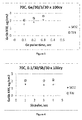
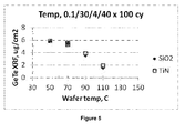
Figure 5 provides the GeTe XRF plotted against wafer temperature (°C) for those films deposited on the SiO2 and TiN substrates in Example 5. -
Figure 6a provides the GeSbTe XRF using 50 ALD cycles consisting of 1 GeTe sequence and 1 SbTe sequence on a silicon oxide substrate in Example 6. -
Figure 6b provides the GeSbTe XRF using 50 ALD cycles consisting of 1 GeTe sequence and 1 SbTe sequence on a titanium nitride substrate in Example 6. -
Figure 7a provides the GeSbTe XRF plotted against cycle number for those films deposited on the silicon oxide substrate in Example 7. -
Figure 7b provides the GeSbTe XRF plotted against cycle number for those films deposited on a titanium nitride substrate in Example 7. - To fabricate high density electronic devices such as phase change memory (PCRAM) or photovoltaic materials, Atomic Layer Deposition (ALD) is a preferred technology to deposit films, such as metal chalcogenide films, uniformly on small dimensional structures on a substrate surface. In certain embodiments, the film comprises a metal chalcogenide film. The term "metal chalcogenide" as used herein refers to a film that contains one or more Group 16 ion (chalcogenide) and at least one electropositive element. Examples of chalcogenide materials include, but are not limited to, sulfides, selenides, and tellurides. Conventional ALD technology involves ALD reactors which typically operate under vacuum and at elevated temperature. It also requires that the precursors be volatile and thermally stable compounds in order to be delivered to the reactor chamber in the vapor phase. ALD is a type of chemical vapor deposition that is used for highly controlled deposition of thin films. It is a self-limiting (e.g., the amount of film material deposited in each reaction cycle is constant) and sequential (e.g., the precursor vapors are brought onto the substrates alternately, one at a time, separated by purging periods with inert gas) process. ALD is considered a deposition method with the greatest potential for producing very thin, conformal films with control of the thickness and composition of the films possible at the atomic level. Using ALD, film thickness depends only on the number of reaction cycles, which makes the thickness control accurate and simple.
- Described herein are methods and precursors for depositing germanium-containing films are multi-component films such as without limitation GeTe and GeTeSb films. Exemplary depositions temperatures for the method described here include ranges having any one or more of the following endpoints: 500, 400, 300, 200, 195, 190, 185, 180, 175, 170, 165, 160, 155, 150, 145, 140, 135, 130, 125, 120, 115, 110, 105, 100, 95, 90, 85, 80, 75, 70, 65, 60, 55, 50, 45, 40, 35, 30, 25, and/or 20°C. Examples of particular temperature ranges include, but are not limited to, from about 20 to about 200°C or from about 50 to about 100°C.
- In certain embodiments, the germanium-containing films further comprise tellurium and are deposited using a tellurium precursor. Exemplary tellurium precursors can be selected from disilyltellurium, silylalkyltellurium, silylaminotellurium with the general structures of:
(R1R2R3Si)2Te (R1R2R3Si)TeR4 (R1R2R3Si)TeN(R4R5)
where R1, R2, R3, R4, and R5 are independently selected from hydrogen, an alkyl group having 1 - 10 carbons in linear, branched, or cyclic forms without or with double bonds, or a C3 to C10 aryl group. - In an ALD process, the tellurium precursors, alcohols, germanium and antimony precursors, such as (Me2N)4Ge and (Me2N)3Sb are suitably introduced to a deposition chamber in any sequence in a cyclic manner by vapor draw or direct liquid injection (DLI). The deposition temperature is preferably between 25° to 500° C.
- One embodiment of the method for depositing a multicomponent film onto at least a portion of a substrate comprises the steps of:
- a) contacting the substrate with a Ge precursor comprising HGeCl3 to react with the substrate and provide a first coating layer comprising Ge;
- b) introducing a purge gas to remove any unreacted Ge precursor;
- c) contacting the first coating layer comprising Ge with a Te precursor wherein at least a portion of the Te precursor reacts with the Ge comprised therein to provide a second coating layer comprising Ge and Te;
- d) introducing a purge gas to remove any unreacted Te precursor;
- e) contacting the second coating layer comprising Ge and Te with a Sb precursor, wherein at least a portion of the Sb precursor reacts with at least a portion of the Ge and Te comprised therein to provide a third coating layer comprising Ge, Te, and Sb; and
- f) introducing a purge gas to remove any unreacted Sb precursor.
- In certain embodiments, steps (a) through (f) are repeated a number of times until a desired thickness of coating layers is reached to provide the multicomponent film. In this or other embodiment, the steps may be performed in the order of:
- e → f → → a → b → c → d.
- Another embodiment of the method for depositing a multicomponent film onto at least a portion of a substrate comprises the steps:
- a) Introducing HGeCl3 to react with substrate to cover the substrate surface with Ge-Cl fragments
- b) Purging with inert gas
- c) Introducing a Te precursor to provide a Te layer and
- d) Purging with inert gas to remove any reaction by-products.
- The ALD cycle is repeated a certain number of times until the desired film thickness is achieved. In the above embodiment, the next ALD cycle starts with Steps a) to d) and the steps are repeated until the desired thickness of film is obtained.
- In yet another embodiment, the method for depositing a multicomponent film onto at least a portion of a substrate comprises the steps:
- a) introducing a Sb precursor to form a Sb layer comprising aminoantimony on the surface of the substrate
- b) purging with inert gas to remove any reaction by-products
- c) introducing a Te precursors to react with aminoantimony layer to form Sb-Te with a Te layer comprising silyl groups
- d) purging with inert gas to remove any reaction by-products
- e) introducing a Ge precursor comprising HGeCl3 to react with remaining silyl groups on tellurium layer to form Te-Ge bonds with a Ge layer comprising Ge-Cl groups
- f) purging with inert gas
- g) introducing a Te precursors to react with aminoantimony layer to form Sb-Te with a Te layer comprising silyl groups and
- h) purging with inert gas to remove any reaction by-products.
- The ALD cycle is repeated a certain number of times until the desired film thickness is achieved. In the above embodiment, the next ALD cycle starts with Step a through Step h which cycle is then repeated until the desired thickness of film is obtained. In this or other embodiment, the steps may be performed in the order of:
- e → f → g → h → a → b → c → d.
- In certain embodiments, the order of Steps a to h can be alternated to achieve required GST film such as ratio of Ge vs Sb or Ge vs Te.
- Exemplary silyltellurium compounds used in the process described herein have the following formulae:
(R1R2 R3Si)2Te; (R1R2R3Si)TeR4; and (R1R2R3Si)TeN(R4R5)
where R1, R2, R3, R4 and R5 are each individually a hydrogen atom, an alkyl groups with 1 to 10 carbons in a linear, branched, or cyclic form, or aromatic groups with 4 to 10 carbons. - Exemplary aminogermanes, aminoantimony, and antimony alkoxides in the process described herein have the following formulae:
(R1R2N)4Ge (R1R2N)3Sb (R1O)3Sb
where R1 and R2 are each individually alkyl groups with 1 to 10 carbons in linear, branched, or cyclic form. - In the formulae above and throughout the description, the term "aryl" denotes an aromatic cyclic or an aromatic heterocyclic group or an aralkyl group having from 4 to 10 carbon atoms, from 4 to 10, from 5 to 10 carbon atoms, or from 6 to 10 carbon atoms. Exemplary aryl groups include, but are not limited to, pyrrolyl, phenyl, benzyl, chlorobenzyl, tolyl, and o-xylyl.
- In one embodiment, the multicomponent film is deposited using an ALD method. The method described herein can be used to provide a thin film in a deposition apparatus. The deposition apparatus suitably consists of the following parts.
- A reactor where a substrate is placed, precursor vapors react and form films. The reactor walls and substrate holder can be heated at the same or different temperatures;
- One or more liquid or solid precursor containers. The containers may also be heated if needed;
- One or more valves that may switch on or off the vapor flows to the reactor from the precursor containers. A mass flow controller (MFC) unit is used to control when and how
much valves - A vacuum pump that pumps out air or precursor vapors from the reactor. A valve switches on/off the pumping line;
- A vacuum gauge that measures the pressure level within the reactor; and
- An inert or purge gas (e.g. Ar or N2) that switches on or off via a valve.
- In a typical ALD process, the reactor is filled with inert gas (e.g., Ar or N2) through an inlet and then pumped out using a
vacuum pump 8 to a vacuum level below 20 mTorr (2.7 Pa). The reactor is then filled with inlet gas again and the reactor wall and substrate holder are heated to a temperature between 25 °C to 500 °C at which the deposition is set to begin. The Ge precursor is delivered from a precursor container that is heated to a certain temperature range. The temperature remains constant during the deposition. The precursor is delivered from a precursor container that is heated to a temperature between 25 °C and 500 °C. The temperature also remains constant during the deposition. The number of the cycles is preset according to the film thickness that is predetermined. The GST films are formed by repeating the processes for Ge and Sb, respectively. The processes for the growth of Ge and Sb are similar to that for Te. - Existing ALD methods of making GST films from alkoxygermanes, alkoxyantimony, and silyltellurium generate GST films with composition of (GeTe2)x(Sb2Te3)y, with a typical formula of Ge2Sb2Te7 where germanium is tetravalent. Industry preferred GST material is Ge2Sb2Te5 in the composition group of (GeTe)x(Sb2Te3)y, where germanium is divalent. In order to increase germanium content in the film to achieve Ge2Sb2Te5, divalent germanium precursors have to be used. Most of divalent germanium compounds are either unstable or less volatile in a deposition process such as ALD. The method described herein provides, without being bound by theory, in-situ generation of divalent germanium which is used as intermediate to deposit divalent germanium on film surface. In certain embodiments, the trichlorogermane precursor is used to deposit germanium-containing films, such as without limitation, binary films GeTe as well as ternary films such as Ge2Sb2Te5. Described herein is a method for depositing a multi-component film using trichlorogermane as precursor for ALD and CVD deposition of germanium containing thin films, such as GST films for PRAM applications. Trichlorogermane generates dichlorogermylene inside the deposition chamber. Dichlorogermylene reacts with disilyltellurium to form GeTe, which further combines with Sb2Te3 to form phase change material Ge2Sb2Te5 for phase change memory allocations.
- In one embodiment of the method described herein, the germanium precursor HGeCl3 was used for GeTe film deposition having a 1:1 composition by an ALD deposition process. Using the tellurium precursor such as (Si Me3)2Te as a Te precursor, GeTe could be formed as following equations (1) and (2).
HGeCl3 → GeCl2 + HCl (1)
GeCl2 + (SiMe3)2Te→ GeTe + 2Me3SiCl (2)
- The byproduct or equation (2), Me3SiCl is volatile, so that a pure GeTe film can be deposited.
- In another embodiment of the method described herein, the germanium precursor HGeCl3 was used for GeSe film deposition having 1:1 composition by an ALD deposition process. Using the silylselenium precursor such as (Me3Si)2Se as a Se precursor, GeSe could be formed as following equations (3) and (4).
HGeCl3 → GeCl2 + HCl (3)
GeCl2 + (SiMe3)2Se→ GeSe + 2Me3SiCl (4)
- The byproduct or equation (4), Me3SiCl is volatile, so that a pure SeTe film can be deposited.
- Examples of tellurium precursors or Te precursors may comprise disilyltellurium, silylalkyltellurium, or compounds having the general structures of: (R1R2R3Si)2Te and (R1R2R3Si)R4Te. Examples of Selenium or Se precursors may comprise disilylselenium, silylalkylselenium, or compounds having the general structures of: (R1R2R3Si)2Se or (R1R2R3Si)R4Se. In the foregoing formulas, substituents R1, R2, R3, and R4 are each independently: hydrogen; linear, branched, or unsaturated C1-10 alkyl groups; and C4-10 cyclic alkyl groups, or C4-12 aromatic groups. The term "alkyl" as used herein is selected from the group consisting of: linear, branched, or unsaturated C1-10 alkyl groups; and C410 cyclic alkyl groups, preferably from 1 to 6 carbon atoms, more preferably from 1 to 3 carbon atoms, alternately from 3 to 5 carbon atoms, further alternately from 4 to 6 carbons atoms, or variations of the foregoing ranges. Exemplary alkyl groups include, but are not limited to, methyl (Me), ethyl (Et), n-propyl, isopropyl, n-butyl, isobutyl, sec-butyl, tert-butyl, tert-amyl, n-pentyl, n-hexyl, cyclopentyl, and cyclohexyl. The term "alkyl" applies also to alkyl moieties contained in other groups such as haloalkyl, alkylaryl, or arylalkyl. In certain embodiments, some of the groups discussed herein may be substituted with one or more other elements such as, for example, a halogen atom or other heteroatoms such as O, N, Si, or S.
- Examples for the silyltellurium precursor include, but are not limited to, bis(trimethylsilyl)tellurium, bis(dimethylsilyl)tellurium, bis(triethylsilyl)tellurium, bis(diethylsilyl)tellurium, bis(phenyldimethylsilyl)tellurium, bis(t-butyldimethylsilyl)tellurium, dimethylsilylmethyltellurium, dimethylsilylphenyltellurium, dimethylsilyl-n-butyltellurium, dimethylsilyl-t-butyltellurium, trimethylsilylmethyltellurium, trimethylsilylphenyltellurium, trimethylsilyl-n-butyltellurium, and trimethylsilyl-t-butyltellurium.
- Examples for the silylselenium precursor include, but are not limited to, bis(trimethylsilyl)selenium, bis(dimethylsilyl)selenium, bis(triethylsilyl)selenium, bis(diethylsilyl)selenium, bis(phenyldimethylsilyl)selenium, bis(t-butyldimethylsilyl)selenium, dimethylsilylmethylselenium.
- The deposited films that can be made in accordance with the methods described herein are selected from the group selected from Germanium Tellurium (GT), Antimony Germanium (SG), Germanium Antimony Tellurium (GST), Germanium Oxide, and Germanium Nitride.
- In one particular embodiment, the GST film is deposited using trichlorogermane. Trichlorogermane has an unique property. It is in equilibrium with germanium dichloride and HCl at room temperature (see equation (3)).
HGeCl3 ⇄ GeCl2 +HCl Equation 3
- Germanium dichloride and HCl form a loosely bonded complex. This complex can be distilled without decomposition (boiling point 75°C) under atmospheric pressure. On the other hand, this complex can be pull apart by high vacuum at low temperature and generate pure germanium dichloride, which is a solid.
- Described herein is a method for using trichlorogermane as germanium precursor for GST films. Trichlorogermane is delivered into ALD reactor chamber in vapor phase. The molecule is decomposed into germanium dichloride and HCl by low pressure to allow germanium dichloride to anchor on the substrate surface, and consequently reacts with disilyltellurium in ALD cycles to form GT films such as GeTe films, or GST films with disilyltellurium and antimony alkoxides such as antimony ethoxide or aminoantimony such as tris(dimethylamino)antimony as antimony (Sb) precursors.
GeCl2 + (Me3Si)2Te → GeTe + Me3SiCl
Sb(OEt)3 + (Me3Si)2Te → Sb2Te3 + Me3SiOEt
Sb(NMe2)3 + (Me3Si)2Te → Sb2Te3 + Me3SiNMe2
GeTe + Sb2Te3 → (GeTe)x(Sb2Te3)y
- Germanium dichloride also reacts with trisilylantimony to form Ge3Sb2 films
GeCl2 + (Me3Si)3Sb → Ge3Sb2 + Me3SiCl
- Examples for the aminoantimony include, but are not limited to, tris(dimethylamino)antimony, tris(diethylamino)antimony, tris(di-iso-propylamino)antimony, tris(di-n-propylamino)antimony, tris(di-sec-butylamino)antimony, and tris(di-tert-butylamino)antimony.
- Examples for the antimony alkoxides include, but are not limited to, antimony ethoxide ((EtO)3Sb), antimony methoxide ((MeO)3Sb), antimony iso-propoxide ((iPrO)3Sb), antimony n-propoxide ((nPrO)3Sb), antimony sec-butoxide ((sBuO)3Sb), antimony tert-butoxide ((tBuO)3Sb).
- Examples for the trisilylantimony precursors include, but are not limited to, tris(trimethylsilyl)antimony, tris(dimethylsilyl)antimony, tris(triethylsilyl)antimony, tris(diethylsilyl)antimony, tris(phenyldimethylsilyl)antimony, tris(t-butyldimethylsilyl)antimony.
- Deposition was performed in an ALD reactor manufactured by Quros reactor with a shower head type PEALD chamber with a load lock, which can handle one 4 inch (10 cm) wafer. The phase transition properties of samples and films were characterized by Energy Dispersive X-ray Analysis.
- A GeTe film was obtained in the following manner. The HGeCl3 canister temperature was around 1°C, and (Me3Si)2Te canister temperature was at 40°C. A typical wafer temperature is 70°C, typical Ar gas flow rate is 500 sccm (standard cubic centimetres per minute), and the reactor pressure is controlled at 3 Torr (400 Pa). The film was deposited in the following manner after a wafer was loaded on a heated susceptor in the reactor and Ar gas was flowing into the reactor for a few minutes.
- a) Ge precursor pulse step; HGeCl3 vapor is introduced into the reactor for typically 0.1 sec using a vapor draw method. The vapor draw method used herein means that the vapor of a precursor comes from a canister without any help of a carrier gas, and so only outlet valve of the canister opens at a pulse step.
- b) Ar (Ge) purge step; Ar gas flows into the reactor for seconds to remove any unreacted Ge species and reaction by-products.
- c) Te precursor pulse step; (Me3Si)2Te vapor is introduced into the reactor for a few seconds by Ar carrier gas (50 sccm) flowing through the Te canister.
- d) Ar (Te) purge step; Ar gas flows into the reactor for seconds to remove any unreacted Te species, and reaction byproducts.
- Steps a) to d) were repeated 100 times to obtain a required film thickness.
- Using the above procedure, both silicon oxide and titanium nitride as substrate, trichlorogermane as Ge precursor, and bis(trimethylsilyl)tellurium as Te precursor, GeTe films were deposited in the sequence in each cycle were tested: (1) various seconds of Ge pulse; (2) 30 seconds Ar purge; (3) 4 seconds Te pulse; and (4) 40 seconds Ar purge. XRF indicated the Ge/Te atomic ratio is 1:1.
Figure 1 provides the GeTe XRF compared to Ge pulse time (seconds) for those films deposited on the SiO2 and TiN substrates. The same result can be obtained when the Te precursor pulse step is applied first instead of the Ge precursor pulse step. - Using a procedure similar to that described in Example 1 and silicon oxide and titanium nitride as substrates, trichlorogermane as Ge precursor, and bis(trimethylsilyl)tellurium as Te precursor, GeTe films were deposited via ALD. 100 ALD cycles with the following sequence in each cycle were tested: (1) 0.1 second Ge pulse; (2) 20 seconds Ar purge; (3) various seconds of Te pulse; and (4) 20 seconds Ar purge. XRF indicated the Ge/Te atomic ratio of 1:1.
Figure 2 provides the GeTe XRF compared to Te pulse time (seconds) for those films deposited on the SiO2 and TiN substrates. - Using a procedure similar to that described in Example 1 and silicon oxide and titanium nitride as substrates, trichlorogermane as Ge precursor, and tris(trimethylsilyl)antimony as Sb precursor rather than a Te precursor, GS films were deposited via ALD. 100 ALD cycles with the following sequence in each cycle were tested: (1) various seconds of Ge precursor pulse; (2) 30 seconds Ar purge; (3) 3 seconds Sb precursor pulse; and (4) 30 seconds Ar purge. XRF indicated the Ge/Sb atomic ratio of 1:1.
Figure 3 provides the GeSb XRF compared to Sb precursor pulse time (seconds) for those films deposited on the SiO2 and TiN substrates. - Using a procedure similar to that described in Example 1 and silicon oxide and titanium nitride as substrates, trichlorogermane as Ge precursor, and tris(trimethylsilyl)antimony as Sb precursor rather than a Te precursor, GeSb films were deposited via ALD. 100 ALD cycles with the following sequence in each cycle were tested: (1) 0.1 second Ge precursor pulse; (2) 20 seconds Ar purge; (3) various senconds of Sb precursor pulse; and (4) 20 seconds Ar purge. XRF indicated the Ge/Sb atomic ratio of 1:1.
Figure 4 provides the GeSb XRF compared to Sb pulse time (seconds) for those films deposited on the SiO2 and TiN substrates. - Using the above procedure, both silicon oxide and titanium nitride as substrate, trichlorogermane as Ge precursor, and bis (trimethylsilyl)tellurium as Te precursor, 100 ALD cycles with the following sequence in each cycle were tested: (1) 0.1 second Ge precursor pulse; (2) 30 seconds Ar purge; (3) 4 seconds Te precursor pulse; and (4) 40 seconds Ar purge. The resulting data show that the GeTe deposition rates decreased as the temperatures increased in the temperature range of 50 to 110°C.
Figure 5 provides the GeTe XRF compared to substrate temperature (degrees celsius) for those films deposited on the SiO2 and TiN substrates. - The above examples show that GeTe films exhibited 1:1 compositions under the ALD deposition conditions described above. Saturation conditions with these precursors, and GeTe deposition rate at 70°C was 1.16 A/cycle. Deposition rate decreased gradually with increase of substrate temperatures. XPS results showed very low Cl and C impurities in the GeTe film.
- Ge-Sb-Te ternary films were deposited in a shower-head-type ALD reactor with a 6-inch (15 cm)wafer scale(CN-1, Atomic-premium) at temperatures ranging from 50°C to 120°C using HGeCl3 as the Ge precursor, Sb(OEt)3 as the Sb precursor, and Te(SiMe3)2 as the Te precursor. The HGeCl3 canister temperature was around 1°C, Sb(OEt)3 canister temperature was at 40°C, and Te(SiMe3)2 canister temperature was at 40°C. The film composition was determined by XRF.
- Using a procedure similar to that described in Example 1, except that the antimony precursor is introduced first, and silicon oxide and titanium nitride as substrates, bis(trimethylsilyl)tellurium as Te precursor and antimony ethoxide as Sb precursor rather than a Ge precursor, SbTe films were deposited via ALD. Combining SbTe deposition procedure and GeTe deposition procedure (from Example 1) can deposit GeSbTe films by repeating a) to d) steps in procedure using Sb/Te or Ge/Te precursors (called GeTe sequence and SbTe sequence, repectively).
Figures 6a and 6b provides the GeSbTe XRF using 50 ALD cycles consisting of 1 GeTe sequence and 1 SbTe sequence on silicon oxide and titanium nitride substrates, respectively. The total layer density was 4.31 ug cm-2 on the SiO2 substrate and 4.84 ug cm-2 on the TiN substrate. The number of each sequence in one ALD cycle can be modified to change the composition of films. - Using a procedure similar to that described in Example 6 and silicon oxide and titanium nitride as substrates, trichlorogermane as Ge precursor, antimony ethoxide as Sb precursor and bis(trimethylsilyl)tellurium as Te precursor, GeSbTe ternary film were deposited. Various number of cycles was tested with the following sequence in each cycle: (a) 3 seconds of Sb precursor pulse; (b) 15 seconds Ar purge; (c) 1 second of Te precursor pulse; (d) 15 seconds of Ar purge; (e) 5 seconds of Ge precursor pulse; (f) 15 seconds of Ar purge; (g) 1 second of Te precursor pulse; and (h) 15 seconds of Ar purge.
Figures 7a and 7b provides the GeSbTe XRF compared to cycle number for those films deposited on the silicon oxide and titanium nitride substrates, respectively. By the procedure, Ge:Sb:Te ratio of 15:35:50 film was deposited. - The aforementioned examples are merely illustrative, and do not limit this dislocsure in any way. While the method and precursor compositions have been described in detail and with reference to specific examples and the embodiments thereof, it will be apparent to one skilled in the art that various changes and modifications can be made therein without departing from the spirit and scope thereof.
Claims (12)
- A method for depositing a germanium-containing film onto at least a portion of a substrate comprising the steps of:providing the substrate within a reactor; andintroducing into the reactor a Ge precursor comprising HGeCl3 under deposition conditions sufficient to react with the substrate and provide the film.
- A method as claimed in Claim 1 of depositing a multicomponent film on at least a portion of a substrate comprising steps (a) to (d) and optionally steps (e) and (f):a) contacting the substrate with a Ge precursor comprising HGeCl3 to react with the substrate and provide a first coating layer comprising Ge;b) introducing a purge gas to remove any unreacted Ge precursor;c) contacting the first coating layer comprising Ge with a Te precursor, wherein at least a portion of the Te precursor reacts with the Ge comprised therein to provide a second coating layer comprising Ge and Te;d) introducing a purge gas to remove any unreacted Te precursor;e) contacting the second coating layer comprising Ge and Te with a Sb precursor, wherein at least a portion of the Sb precursor reacts with at least a portion of the Ge and Te comprised therein to provide a third coating layer comprising Ge, Te, and Sb;f) introducing a purge gas to remove any unreacted Sb precursor;
wherein steps (a) through (d), (a) through (f) and/or (e) through (f) are repeated to form a number of coating layers and provide the film. - The method of Claim 2 wherein the Te precursor comprises a silyltellurium selected from the group consisting of disilyltellurium having a general formula: (R1R2R3Si)2Te; alkylsilyltellurium having a general formula: (R1R2R3Si)TeR4; and mixtures thereof, wherein R1, R2, R3, and R4 are each independently selected from the group consisting of: hydrogen; linear or branched optionally unsaturated C1-10 alkyl groups; C4-10 cyclic alkyl groups; and C4-12 aromatic groups.
- The method of Claim 3 wherein the Te precursor comprises a disilyltellurium having the following formula: (R1 3Si)2Te, preferably bis(trimethylsilyl)tellurium.
- The method of any one of Claims 2 to 4 wherein the Sb precursor comprises a compound selected from the group consisting of a compound having the general structure (R1O)3Sb; a compound having the general structure(R1R2R3Si)3Sb; and a compound having the general structure (R1R2R3Si)2R4Sb wherein substituents R1, R2, R3, and R4 are each independently: hydrogen; linear or branched optionally unsaturated C1-10 alkyl groups; C4-10 cyclic alkyl groups; and C4-12 aromatic groups; or wherein the Sb precursor comprises a compound having the following formula: SbXn, wherein X is a nucleophilic group selected from the group consisting of F(fluorine), Cl (chlorine), Br (bromine), NR2 (amino), CN (cyano), OCN (cyanate), SCN (thiocyanate), diketonate, carboxylic groups and mixtures thereof; and n equals the oxidation state of Sb, preferably 3.
- The method of Claim 5 wherein the Sb precursor comprises tris(trimethylsilyl)antimony or Sb(OEt)3.
- The method of Claim 1 wherein the method further comprises introducing an oxygen source into the reactor to react with the Ge precursor and provide a germanium oxide film, and wherein the oxygen source preferably comprises at least one selected from the group consisting of oxygen (O2), oxygen plasma, ozone (O3), hydrogen peroxide, air, nitrous oxide, water plasma, and water.
- The method of Claim 1 wherein the method further comprises introducing a nitrogen source into the reactor to react with the Ge precursor and provide a germanium nitride film, wherein the nitrogen source preferably comprises at least one selected from the group consisting of ammonia, ammonia plasma, nitrogen/hydrogen plasma, and nitrogen plasma.
- The method of Claim 1 wherein the method further comprises introducing hydrogen plasma into the reactor to react with the Ge precursor and provide a germanium film.
- A method of depositing a multicomponent film on at least a portion of a substrate comprising the steps of:a) introducing a Sb precursor to form a Sb layer comprising aminoantimony on the surface of the substrate;b) purging with inert gas to remove any reaction by-products;c) introducing a Te precursor to react with aminoantimony layer to form Sb-Te with a Te layer comprising silyl groups;d) purging with inert gas to remove any reaction by-products;e) introducing a Ge precursor comprising HGeCl3 to react with remaining silyl groups on tellurium layer to form Te-Ge bonds with a Ge layer comprising Ge-Cl groups;f) purging with inert gas;g) introducing a Te precursor to react with aminoantimony layer to form Sb-Te with a Te layer comprising silyl groups; andh) purging with inert gas to remove any reaction by-products;wherein steps a) through h) are repeated to form a number of coating layers and provide GST film.
- The method of Claim 10 wherein the Te precursor is as defined in Claim 3 or Claim 4.
- The method of Claim 10 or Claim 11 wherein the Sb precursor is as defined in Claim 5 or Claim 6.
Applications Claiming Priority (2)
| Application Number | Priority Date | Filing Date | Title |
|---|---|---|---|
| US201361810919P | 2013-04-11 | 2013-04-11 | |
| US14/245,403 US9214630B2 (en) | 2013-04-11 | 2014-04-04 | Method of making a multicomponent film |
Publications (2)
| Publication Number | Publication Date |
|---|---|
| EP2789712A1 true EP2789712A1 (en) | 2014-10-15 |
| EP2789712B1 EP2789712B1 (en) | 2017-01-25 |
Family
ID=50488987
Family Applications (1)
| Application Number | Title | Priority Date | Filing Date |
|---|---|---|---|
| EP14164386.6A Not-in-force EP2789712B1 (en) | 2013-04-11 | 2014-04-11 | Method of making a multicomponent film |
Country Status (6)
| Country | Link |
|---|---|
| US (2) | US9214630B2 (en) |
| EP (1) | EP2789712B1 (en) |
| JP (2) | JP5902743B2 (en) |
| KR (2) | KR101634742B1 (en) |
| CN (1) | CN104099578B (en) |
| TW (1) | TWI507562B (en) |
Cited By (1)
| Publication number | Priority date | Publication date | Assignee | Title |
|---|---|---|---|---|
| WO2024133713A1 (en) * | 2022-12-23 | 2024-06-27 | Umicore Ag & Co. Kg | Inorganic compounds |
Families Citing this family (18)
| Publication number | Priority date | Publication date | Assignee | Title |
|---|---|---|---|---|
| US9214630B2 (en) * | 2013-04-11 | 2015-12-15 | Air Products And Chemicals, Inc. | Method of making a multicomponent film |
| US20170088951A1 (en) * | 2014-10-17 | 2017-03-30 | Eric R. Dickey | Deposition of high-quality mixed oxide barrier films |
| US20160108524A1 (en) * | 2014-10-17 | 2016-04-21 | Lotus Applied Technology, Llc | High-speed deposition of mixed oxide barrier films |
| CN104392931B (en) | 2014-12-03 | 2018-06-22 | 京东方科技集团股份有限公司 | Thin film transistor (TFT) and preparation method thereof, array substrate, display device |
| CN104362298B (en) | 2014-12-03 | 2018-11-06 | 京东方科技集团股份有限公司 | A kind of electrode slice and preparation method thereof, energy storage device |
| US20170073812A1 (en) * | 2015-09-15 | 2017-03-16 | Ultratech, Inc. | Laser-assisted atomic layer deposition of 2D metal chalcogenide films |
| US9607842B1 (en) * | 2015-10-02 | 2017-03-28 | Asm Ip Holding B.V. | Methods of forming metal silicides |
| JP6505619B2 (en) * | 2016-02-09 | 2019-04-24 | 株式会社東芝 | Super lattice memory and cross point memory device |
| CN112429703B (en) * | 2019-08-26 | 2023-03-10 | 天津大学 | A two-dimensional layered tellurium-doped germane and its preparation method |
| US11716861B2 (en) | 2020-12-15 | 2023-08-01 | Micron Technology, Inc. | Electrically formed memory array using single element materials |
| CN113611798B (en) * | 2021-07-02 | 2023-08-29 | 深圳大学 | Multilayer phase-change thin film and preparation method of phase-change memory unit thereof |
| CN113604906B (en) * | 2021-07-07 | 2023-05-12 | 哈尔滨工程大学 | Micro-nano optical phase change fiber for direct writing of static electricity and preparation method and application thereof |
| KR102950735B1 (en) * | 2022-01-18 | 2026-04-08 | 삼성전자주식회사 | A method for forming a GeSbTe film |
| KR102819579B1 (en) * | 2022-12-06 | 2025-06-12 | 한국화학연구원 | Novel germanium precursor, composition for thin film deposition containing the same, and method for manufacturing a thin film employing the same |
| US20240287677A1 (en) * | 2023-02-13 | 2024-08-29 | Micron Technology, Inc. | Atomic layer deposition using tin-based or germanium-based precursors |
| JPWO2024177053A1 (en) | 2023-02-24 | 2024-08-29 | ||
| US20250059646A1 (en) * | 2023-08-15 | 2025-02-20 | Micron Technology, Inc. | Methods for depositing germanium films by atomic layer deposition |
| KR20250125894A (en) * | 2024-02-15 | 2025-08-22 | 에이에스엠 아이피 홀딩 비.브이. | Methods and systems for depositing metalloid layer |
Citations (3)
| Publication number | Priority date | Publication date | Assignee | Title |
|---|---|---|---|---|
| US20030230233A1 (en) * | 1999-09-20 | 2003-12-18 | Fitzgerald Eugene A. | Method of producing high quality relaxed silicon germanium layers |
| US20090162973A1 (en) * | 2007-12-21 | 2009-06-25 | Julien Gatineau | Germanium precursors for gst film deposition |
| EP2083096A1 (en) * | 2008-01-28 | 2009-07-29 | Air Products and Chemicals, Inc. | Antimony precursors for GST Films In ALD/CVD processes |
Family Cites Families (39)
| Publication number | Priority date | Publication date | Assignee | Title |
|---|---|---|---|---|
| JPS61234030A (en) | 1985-04-09 | 1986-10-18 | Canon Inc | Forming method for accumulated film |
| JPS61281870A (en) | 1985-06-07 | 1986-12-12 | Canon Inc | Deposited film formation method |
| JPS61283111A (en) | 1985-06-10 | 1986-12-13 | Canon Inc | Forming method for accumulated film |
| JPH0715585B2 (en) * | 1985-09-27 | 1995-02-22 | 松下電器産業株式会社 | Photoconductor |
| JPH05218014A (en) * | 1991-11-05 | 1993-08-27 | Oki Electric Ind Co Ltd | Method of forming insulating film |
| JP3332463B2 (en) * | 1992-04-24 | 2002-10-07 | キヤノン株式会社 | Light receiving member for electrophotography |
| JPH08262477A (en) * | 1995-03-20 | 1996-10-11 | Nikon Corp | Method for manufacturing spatial light modulator, and amorphous silicon germanium alloy photoreceptor |
| KR101027485B1 (en) | 2001-02-12 | 2011-04-06 | 에이에스엠 아메리카, 인코포레이티드 | Improved Process for Semiconductor Thin Film Deposition |
| KR100434698B1 (en) | 2001-09-05 | 2004-06-07 | 주식회사 하이닉스반도체 | Method for growing epitaxial layer in semiconductor device |
| WO2004081986A2 (en) | 2003-03-12 | 2004-09-23 | Asm America Inc. | Method to planarize and reduce defect density of silicon germanium |
| JP4714422B2 (en) * | 2003-04-05 | 2011-06-29 | ローム・アンド・ハース・エレクトロニック・マテリアルズ,エル.エル.シー. | Method for depositing germanium-containing film and vapor delivery device |
| JP4954448B2 (en) | 2003-04-05 | 2012-06-13 | ローム・アンド・ハース・エレクトロニック・マテリアルズ,エル.エル.シー. | Organometallic compounds |
| JP4689969B2 (en) | 2003-04-05 | 2011-06-01 | ローム・アンド・ハース・エレクトロニック・マテリアルズ,エル.エル.シー. | Preparation of Group IVA and Group VIA compounds |
| US7078300B2 (en) * | 2003-09-27 | 2006-07-18 | International Business Machines Corporation | Thin germanium oxynitride gate dielectric for germanium-based devices |
| KR100640620B1 (en) | 2004-12-27 | 2006-11-02 | 삼성전자주식회사 | NOR type flash memory device of twin bit cell structure and manufacturing method thereof |
| US7358194B2 (en) * | 2005-08-18 | 2008-04-15 | Tokyo Electron Limited | Sequential deposition process for forming Si-containing films |
| EP2018642A4 (en) * | 2006-05-12 | 2009-05-27 | Advanced Tech Materials | Low temperature deposition of phase change memory materials |
| KR100807223B1 (en) | 2006-07-12 | 2008-02-28 | 삼성전자주식회사 | Phase change material layer, phase change material layer formation method and manufacturing method of phase change memory device using same |
| EP1883103A3 (en) * | 2006-07-27 | 2008-03-05 | Interuniversitair Microelektronica Centrum | Deposition of group III-nitrides on Ge |
| CN101495672B (en) | 2006-11-02 | 2011-12-07 | 高级技术材料公司 | Antimony and germanium compounds useful for CVD/ALD of metal thin films |
| US7598170B2 (en) * | 2007-01-26 | 2009-10-06 | Asm America, Inc. | Plasma-enhanced ALD of tantalum nitride films |
| JP5337380B2 (en) * | 2007-01-26 | 2013-11-06 | 株式会社半導体エネルギー研究所 | Semiconductor device and manufacturing method thereof |
| CN101678665B (en) * | 2007-04-02 | 2013-07-10 | 代表亚利桑那州立大学行事的亚利桑那董事会 | Novel methods for making and using halosilylgermanes |
| US8377341B2 (en) | 2007-04-24 | 2013-02-19 | Air Products And Chemicals, Inc. | Tellurium (Te) precursors for making phase change memory materials |
| US8454928B2 (en) | 2007-09-17 | 2013-06-04 | L'air Liquide Societe Anonyme Pour L'etude Et L'exploitation Des Procedes Georges Claude | Tellurium precursors for GST deposition |
| US8372489B2 (en) * | 2007-09-28 | 2013-02-12 | Tel Epion Inc. | Method for directional deposition using a gas cluster ion beam |
| SG178736A1 (en) | 2007-10-31 | 2012-03-29 | Advanced Tech Materials | Amorphous ge/te deposition process |
| KR101580575B1 (en) | 2008-04-25 | 2015-12-28 | 에이에스엠 인터내셔널 엔.브이. | Synthesis and use of precursors for ALD of tellurium and selenium thin films |
| US8765223B2 (en) | 2008-05-08 | 2014-07-01 | Air Products And Chemicals, Inc. | Binary and ternary metal chalcogenide materials and method of making and using same |
| US8636845B2 (en) * | 2008-06-25 | 2014-01-28 | L'Air Liquide, Société Anonyme pour l'Etude et l'Exploitation des Procédés Georges Claude | Metal heterocyclic compounds for deposition of thin films |
| US8372483B2 (en) | 2008-06-27 | 2013-02-12 | Asm International N.V. | Methods for forming thin films comprising tellurium |
| TW201247589A (en) | 2009-05-22 | 2012-12-01 | Advanced Tech Materials | Low temperature GST process |
| WO2011027321A1 (en) * | 2009-09-02 | 2011-03-10 | L'air Liquide, Societe Anonyme Pour L'etude Et L'exploitation Des Procedes Georges Claude | Dihalide germanium(ii) precursors for germanium-containing film depositions |
| JP2011074413A (en) * | 2009-09-29 | 2011-04-14 | Tokyo Electron Ltd | Film deposition apparatus, film deposition method, and substrate processing apparatus |
| US8193027B2 (en) * | 2010-02-23 | 2012-06-05 | Air Products And Chemicals, Inc. | Method of making a multicomponent film |
| JP5624083B2 (en) * | 2011-06-09 | 2014-11-12 | エア プロダクツ アンド ケミカルズ インコーポレイテッドAir Productsand Chemicalsincorporated | Binary and ternary metal chalcogenide materials and methods for making and using the same |
| WO2013027682A1 (en) | 2011-08-19 | 2013-02-28 | 東京エレクトロン株式会社 | Method for forming ge-sb-te film, method for forming ge-te film, method for forming sb-te film, and program |
| JP5780981B2 (en) | 2012-03-02 | 2015-09-16 | 東京エレクトロン株式会社 | Method for forming germanium thin film |
| US9214630B2 (en) * | 2013-04-11 | 2015-12-15 | Air Products And Chemicals, Inc. | Method of making a multicomponent film |
-
2014
- 2014-04-04 US US14/245,403 patent/US9214630B2/en active Active
- 2014-04-11 JP JP2014082211A patent/JP5902743B2/en active Active
- 2014-04-11 EP EP14164386.6A patent/EP2789712B1/en not_active Not-in-force
- 2014-04-11 KR KR1020140043785A patent/KR101634742B1/en active Active
- 2014-04-11 CN CN201410146690.1A patent/CN104099578B/en active Active
- 2014-04-11 TW TW103113480A patent/TWI507562B/en active
-
2015
- 2015-11-13 US US14/940,340 patent/US9543517B2/en active Active
-
2016
- 2016-03-03 JP JP2016040969A patent/JP6371322B2/en active Active
- 2016-06-15 KR KR1020160074555A patent/KR102193609B1/en active Active
Patent Citations (3)
| Publication number | Priority date | Publication date | Assignee | Title |
|---|---|---|---|---|
| US20030230233A1 (en) * | 1999-09-20 | 2003-12-18 | Fitzgerald Eugene A. | Method of producing high quality relaxed silicon germanium layers |
| US20090162973A1 (en) * | 2007-12-21 | 2009-06-25 | Julien Gatineau | Germanium precursors for gst film deposition |
| EP2083096A1 (en) * | 2008-01-28 | 2009-07-29 | Air Products and Chemicals, Inc. | Antimony precursors for GST Films In ALD/CVD processes |
Cited By (1)
| Publication number | Priority date | Publication date | Assignee | Title |
|---|---|---|---|---|
| WO2024133713A1 (en) * | 2022-12-23 | 2024-06-27 | Umicore Ag & Co. Kg | Inorganic compounds |
Also Published As
| Publication number | Publication date |
|---|---|
| CN104099578B (en) | 2018-12-07 |
| US9214630B2 (en) | 2015-12-15 |
| US20140308802A1 (en) | 2014-10-16 |
| JP6371322B2 (en) | 2018-08-08 |
| KR101634742B1 (en) | 2016-07-11 |
| KR20140123451A (en) | 2014-10-22 |
| JP5902743B2 (en) | 2016-04-13 |
| TWI507562B (en) | 2015-11-11 |
| TW201447039A (en) | 2014-12-16 |
| EP2789712B1 (en) | 2017-01-25 |
| US20160087207A1 (en) | 2016-03-24 |
| KR102193609B1 (en) | 2020-12-21 |
| CN104099578A (en) | 2014-10-15 |
| US9543517B2 (en) | 2017-01-10 |
| JP2016121403A (en) | 2016-07-07 |
| KR20160073369A (en) | 2016-06-24 |
| JP2015007279A (en) | 2015-01-15 |
Similar Documents
| Publication | Publication Date | Title |
|---|---|---|
| US9543517B2 (en) | Method of making a multicomponent film | |
| CN101792900B (en) | Binary and ternary metal chalcogenide materials and method of making and using the same | |
| JP5290638B2 (en) | Method for depositing metal silicon nitride | |
| KR101012921B1 (en) | Tellurium Precursor for WST Film in Al or Cd Process | |
| KR101379651B1 (en) | Binary and ternary metal chalcogenide materials and method of making and using same | |
| EP1995236B1 (en) | Tellurium (Te) precursors for making phase change memory materials | |
| US8679894B2 (en) | Low temperature deposition of phase change memory materials | |
| JP5778648B2 (en) | Silylantimony precursor and atomic layer deposition (ALD) method using the same | |
| US8507040B2 (en) | Binary and ternary metal chalcogenide materials and method of making and using same | |
| KR101295031B1 (en) | Plasma enhanced cyclic deposition method of metal silicon nitride film |
Legal Events
| Date | Code | Title | Description |
|---|---|---|---|
| PUAI | Public reference made under article 153(3) epc to a published international application that has entered the european phase |
Free format text: ORIGINAL CODE: 0009012 |
|
| 17P | Request for examination filed |
Effective date: 20140411 |
|
| AK | Designated contracting states |
Kind code of ref document: A1 Designated state(s): AL AT BE BG CH CY CZ DE DK EE ES FI FR GB GR HR HU IE IS IT LI LT LU LV MC MK MT NL NO PL PT RO RS SE SI SK SM TR |
|
| AX | Request for extension of the european patent |
Extension state: BA ME |
|
| R17P | Request for examination filed (corrected) |
Effective date: 20141027 |
|
| RBV | Designated contracting states (corrected) |
Designated state(s): AL AT BE BG CH CY CZ DE DK EE ES FI FR GB GR HR HU IE IS IT LI LT LU LV MC MK MT NL NO PL PT RO RS SE SI SK SM TR |
|
| 17Q | First examination report despatched |
Effective date: 20160203 |
|
| REG | Reference to a national code |
Ref country code: DE Ref legal event code: R079 Ref document number: 602014006303 Country of ref document: DE Free format text: PREVIOUS MAIN CLASS: C23C0016220000 Ipc: H01L0045000000 |
|
| RIN1 | Information on inventor provided before grant (corrected) |
Inventor name: IVANOV, SERGEI VLADIMIROVICH Inventor name: GWON, TAE HONG Inventor name: BUCHANANA, IAIN Inventor name: KIM, MOO-SUNG Inventor name: LEI, XINJIAN Inventor name: HWANG, CHEOL SEONG Inventor name: XIAO, MANCHAO |
|
| GRAP | Despatch of communication of intention to grant a patent |
Free format text: ORIGINAL CODE: EPIDOSNIGR1 |
|
| RIC1 | Information provided on ipc code assigned before grant |
Ipc: H01L 45/00 20060101AFI20160715BHEP Ipc: C23C 16/455 20060101ALI20160715BHEP Ipc: C23C 16/30 20060101ALI20160715BHEP |
|
| INTG | Intention to grant announced |
Effective date: 20160824 |
|
| GRAS | Grant fee paid |
Free format text: ORIGINAL CODE: EPIDOSNIGR3 |
|
| GRAA | (expected) grant |
Free format text: ORIGINAL CODE: 0009210 |
|
| AK | Designated contracting states |
Kind code of ref document: B1 Designated state(s): AL AT BE BG CH CY CZ DE DK EE ES FI FR GB GR HR HU IE IS IT LI LT LU LV MC MK MT NL NO PL PT RO RS SE SI SK SM TR |
|
| REG | Reference to a national code |
Ref country code: GB Ref legal event code: FG4D |
|
| REG | Reference to a national code |
Ref country code: CH Ref legal event code: EP |
|
| REG | Reference to a national code |
Ref country code: AT Ref legal event code: REF Ref document number: 864579 Country of ref document: AT Kind code of ref document: T Effective date: 20170215 |
|
| REG | Reference to a national code |
Ref country code: IE Ref legal event code: FG4D |
|
| REG | Reference to a national code |
Ref country code: DE Ref legal event code: R096 Ref document number: 602014006303 Country of ref document: DE |
|
| REG | Reference to a national code |
Ref country code: FR Ref legal event code: PLFP Year of fee payment: 4 |
|
| REG | Reference to a national code |
Ref country code: LT Ref legal event code: MG4D |
|
| REG | Reference to a national code |
Ref country code: NL Ref legal event code: MP Effective date: 20170125 |
|
| REG | Reference to a national code |
Ref country code: AT Ref legal event code: MK05 Ref document number: 864579 Country of ref document: AT Kind code of ref document: T Effective date: 20170125 |
|
| PG25 | Lapsed in a contracting state [announced via postgrant information from national office to epo] |
Ref country code: NL Free format text: LAPSE BECAUSE OF FAILURE TO SUBMIT A TRANSLATION OF THE DESCRIPTION OR TO PAY THE FEE WITHIN THE PRESCRIBED TIME-LIMIT Effective date: 20170125 |
|
| PG25 | Lapsed in a contracting state [announced via postgrant information from national office to epo] |
Ref country code: GR Free format text: LAPSE BECAUSE OF FAILURE TO SUBMIT A TRANSLATION OF THE DESCRIPTION OR TO PAY THE FEE WITHIN THE PRESCRIBED TIME-LIMIT Effective date: 20170426 Ref country code: LT Free format text: LAPSE BECAUSE OF FAILURE TO SUBMIT A TRANSLATION OF THE DESCRIPTION OR TO PAY THE FEE WITHIN THE PRESCRIBED TIME-LIMIT Effective date: 20170125 Ref country code: NO Free format text: LAPSE BECAUSE OF FAILURE TO SUBMIT A TRANSLATION OF THE DESCRIPTION OR TO PAY THE FEE WITHIN THE PRESCRIBED TIME-LIMIT Effective date: 20170425 Ref country code: FI Free format text: LAPSE BECAUSE OF FAILURE TO SUBMIT A TRANSLATION OF THE DESCRIPTION OR TO PAY THE FEE WITHIN THE PRESCRIBED TIME-LIMIT Effective date: 20170125 Ref country code: IS Free format text: LAPSE BECAUSE OF FAILURE TO SUBMIT A TRANSLATION OF THE DESCRIPTION OR TO PAY THE FEE WITHIN THE PRESCRIBED TIME-LIMIT Effective date: 20170525 Ref country code: HR Free format text: LAPSE BECAUSE OF FAILURE TO SUBMIT A TRANSLATION OF THE DESCRIPTION OR TO PAY THE FEE WITHIN THE PRESCRIBED TIME-LIMIT Effective date: 20170125 |
|
| PG25 | Lapsed in a contracting state [announced via postgrant information from national office to epo] |
Ref country code: SE Free format text: LAPSE BECAUSE OF FAILURE TO SUBMIT A TRANSLATION OF THE DESCRIPTION OR TO PAY THE FEE WITHIN THE PRESCRIBED TIME-LIMIT Effective date: 20170125 Ref country code: BG Free format text: LAPSE BECAUSE OF FAILURE TO SUBMIT A TRANSLATION OF THE DESCRIPTION OR TO PAY THE FEE WITHIN THE PRESCRIBED TIME-LIMIT Effective date: 20170425 Ref country code: AT Free format text: LAPSE BECAUSE OF FAILURE TO SUBMIT A TRANSLATION OF THE DESCRIPTION OR TO PAY THE FEE WITHIN THE PRESCRIBED TIME-LIMIT Effective date: 20170125 Ref country code: RS Free format text: LAPSE BECAUSE OF FAILURE TO SUBMIT A TRANSLATION OF THE DESCRIPTION OR TO PAY THE FEE WITHIN THE PRESCRIBED TIME-LIMIT Effective date: 20170125 Ref country code: ES Free format text: LAPSE BECAUSE OF FAILURE TO SUBMIT A TRANSLATION OF THE DESCRIPTION OR TO PAY THE FEE WITHIN THE PRESCRIBED TIME-LIMIT Effective date: 20170125 Ref country code: PT Free format text: LAPSE BECAUSE OF FAILURE TO SUBMIT A TRANSLATION OF THE DESCRIPTION OR TO PAY THE FEE WITHIN THE PRESCRIBED TIME-LIMIT Effective date: 20170525 Ref country code: PL Free format text: LAPSE BECAUSE OF FAILURE TO SUBMIT A TRANSLATION OF THE DESCRIPTION OR TO PAY THE FEE WITHIN THE PRESCRIBED TIME-LIMIT Effective date: 20170125 Ref country code: LV Free format text: LAPSE BECAUSE OF FAILURE TO SUBMIT A TRANSLATION OF THE DESCRIPTION OR TO PAY THE FEE WITHIN THE PRESCRIBED TIME-LIMIT Effective date: 20170125 |
|
| RAP2 | Party data changed (patent owner data changed or rights of a patent transferred) |
Owner name: VERSUM MATERIALS US, LLC |
|
| REG | Reference to a national code |
Ref country code: DE Ref legal event code: R097 Ref document number: 602014006303 Country of ref document: DE |
|
| PG25 | Lapsed in a contracting state [announced via postgrant information from national office to epo] |
Ref country code: RO Free format text: LAPSE BECAUSE OF FAILURE TO SUBMIT A TRANSLATION OF THE DESCRIPTION OR TO PAY THE FEE WITHIN THE PRESCRIBED TIME-LIMIT Effective date: 20170125 Ref country code: CZ Free format text: LAPSE BECAUSE OF FAILURE TO SUBMIT A TRANSLATION OF THE DESCRIPTION OR TO PAY THE FEE WITHIN THE PRESCRIBED TIME-LIMIT Effective date: 20170125 Ref country code: IT Free format text: LAPSE BECAUSE OF FAILURE TO SUBMIT A TRANSLATION OF THE DESCRIPTION OR TO PAY THE FEE WITHIN THE PRESCRIBED TIME-LIMIT Effective date: 20170125 Ref country code: SK Free format text: LAPSE BECAUSE OF FAILURE TO SUBMIT A TRANSLATION OF THE DESCRIPTION OR TO PAY THE FEE WITHIN THE PRESCRIBED TIME-LIMIT Effective date: 20170125 Ref country code: EE Free format text: LAPSE BECAUSE OF FAILURE TO SUBMIT A TRANSLATION OF THE DESCRIPTION OR TO PAY THE FEE WITHIN THE PRESCRIBED TIME-LIMIT Effective date: 20170125 |
|
| REG | Reference to a national code |
Ref country code: DE Ref legal event code: R082 Ref document number: 602014006303 Country of ref document: DE Representative=s name: KADOR & PARTNER PART MBB PATENTANWAELTE, DE Ref country code: DE Ref legal event code: R081 Ref document number: 602014006303 Country of ref document: DE Owner name: VERSUM MATERIALS US, LLC, TEMPE, US Free format text: FORMER OWNER: AIR PRODUCTS AND CHEMICALS, INC., ALLENTOWN, PA., US Ref country code: DE Ref legal event code: R082 Ref document number: 602014006303 Country of ref document: DE Representative=s name: KADOR & PARTNER PARTG MBB PATENTANWAELTE, DE |
|
| PG25 | Lapsed in a contracting state [announced via postgrant information from national office to epo] |
Ref country code: SM Free format text: LAPSE BECAUSE OF FAILURE TO SUBMIT A TRANSLATION OF THE DESCRIPTION OR TO PAY THE FEE WITHIN THE PRESCRIBED TIME-LIMIT Effective date: 20170125 Ref country code: DK Free format text: LAPSE BECAUSE OF FAILURE TO SUBMIT A TRANSLATION OF THE DESCRIPTION OR TO PAY THE FEE WITHIN THE PRESCRIBED TIME-LIMIT Effective date: 20170125 |
|
| REG | Reference to a national code |
Ref country code: CH Ref legal event code: PL |
|
| PLBE | No opposition filed within time limit |
Free format text: ORIGINAL CODE: 0009261 |
|
| STAA | Information on the status of an ep patent application or granted ep patent |
Free format text: STATUS: NO OPPOSITION FILED WITHIN TIME LIMIT |
|
| 26N | No opposition filed |
Effective date: 20171026 |
|
| REG | Reference to a national code |
Ref country code: IE Ref legal event code: MM4A |
|
| PG25 | Lapsed in a contracting state [announced via postgrant information from national office to epo] |
Ref country code: MC Free format text: LAPSE BECAUSE OF FAILURE TO SUBMIT A TRANSLATION OF THE DESCRIPTION OR TO PAY THE FEE WITHIN THE PRESCRIBED TIME-LIMIT Effective date: 20170125 |
|
| PG25 | Lapsed in a contracting state [announced via postgrant information from national office to epo] |
Ref country code: LU Free format text: LAPSE BECAUSE OF NON-PAYMENT OF DUE FEES Effective date: 20170411 Ref country code: SI Free format text: LAPSE BECAUSE OF FAILURE TO SUBMIT A TRANSLATION OF THE DESCRIPTION OR TO PAY THE FEE WITHIN THE PRESCRIBED TIME-LIMIT Effective date: 20170125 Ref country code: CH Free format text: LAPSE BECAUSE OF NON-PAYMENT OF DUE FEES Effective date: 20170430 Ref country code: LI Free format text: LAPSE BECAUSE OF NON-PAYMENT OF DUE FEES Effective date: 20170430 |
|
| REG | Reference to a national code |
Ref country code: FR Ref legal event code: PLFP Year of fee payment: 5 |
|
| REG | Reference to a national code |
Ref country code: BE Ref legal event code: MM Effective date: 20170430 |
|
| PG25 | Lapsed in a contracting state [announced via postgrant information from national office to epo] |
Ref country code: IE Free format text: LAPSE BECAUSE OF NON-PAYMENT OF DUE FEES Effective date: 20170411 |
|
| PG25 | Lapsed in a contracting state [announced via postgrant information from national office to epo] |
Ref country code: BE Free format text: LAPSE BECAUSE OF NON-PAYMENT OF DUE FEES Effective date: 20170430 |
|
| REG | Reference to a national code |
Ref country code: FR Ref legal event code: TP Owner name: VERSUM MATERIALS US, LLC, US Effective date: 20180711 |
|
| PG25 | Lapsed in a contracting state [announced via postgrant information from national office to epo] |
Ref country code: MT Free format text: LAPSE BECAUSE OF NON-PAYMENT OF DUE FEES Effective date: 20170411 |
|
| GBPC | Gb: european patent ceased through non-payment of renewal fee |
Effective date: 20180411 |
|
| PG25 | Lapsed in a contracting state [announced via postgrant information from national office to epo] |
Ref country code: GB Free format text: LAPSE BECAUSE OF NON-PAYMENT OF DUE FEES Effective date: 20180411 |
|
| PG25 | Lapsed in a contracting state [announced via postgrant information from national office to epo] |
Ref country code: HU Free format text: LAPSE BECAUSE OF FAILURE TO SUBMIT A TRANSLATION OF THE DESCRIPTION OR TO PAY THE FEE WITHIN THE PRESCRIBED TIME-LIMIT; INVALID AB INITIO Effective date: 20140411 |
|
| PG25 | Lapsed in a contracting state [announced via postgrant information from national office to epo] |
Ref country code: CY Free format text: LAPSE BECAUSE OF FAILURE TO SUBMIT A TRANSLATION OF THE DESCRIPTION OR TO PAY THE FEE WITHIN THE PRESCRIBED TIME-LIMIT Effective date: 20170125 |
|
| PG25 | Lapsed in a contracting state [announced via postgrant information from national office to epo] |
Ref country code: MK Free format text: LAPSE BECAUSE OF FAILURE TO SUBMIT A TRANSLATION OF THE DESCRIPTION OR TO PAY THE FEE WITHIN THE PRESCRIBED TIME-LIMIT Effective date: 20170125 |
|
| PG25 | Lapsed in a contracting state [announced via postgrant information from national office to epo] |
Ref country code: TR Free format text: LAPSE BECAUSE OF FAILURE TO SUBMIT A TRANSLATION OF THE DESCRIPTION OR TO PAY THE FEE WITHIN THE PRESCRIBED TIME-LIMIT Effective date: 20170125 |
|
| PG25 | Lapsed in a contracting state [announced via postgrant information from national office to epo] |
Ref country code: AL Free format text: LAPSE BECAUSE OF FAILURE TO SUBMIT A TRANSLATION OF THE DESCRIPTION OR TO PAY THE FEE WITHIN THE PRESCRIBED TIME-LIMIT Effective date: 20170125 |
|
| PGFP | Annual fee paid to national office [announced via postgrant information from national office to epo] |
Ref country code: FR Payment date: 20210310 Year of fee payment: 8 |
|
| PGFP | Annual fee paid to national office [announced via postgrant information from national office to epo] |
Ref country code: DE Payment date: 20210316 Year of fee payment: 8 |
|
| REG | Reference to a national code |
Ref country code: DE Ref legal event code: R119 Ref document number: 602014006303 Country of ref document: DE |
|
| REG | Reference to a national code |
Ref country code: DE Ref legal event code: R079 Ref document number: 602014006303 Country of ref document: DE Free format text: PREVIOUS MAIN CLASS: H01L0045000000 Ipc: H10N0070000000 |
|
| PG25 | Lapsed in a contracting state [announced via postgrant information from national office to epo] |
Ref country code: FR Free format text: LAPSE BECAUSE OF NON-PAYMENT OF DUE FEES Effective date: 20220430 Ref country code: DE Free format text: LAPSE BECAUSE OF NON-PAYMENT OF DUE FEES Effective date: 20221103 |