EP2787583A1 - Quantum cascade laser manufacturing method - Google Patents
Quantum cascade laser manufacturing method Download PDFInfo
- Publication number
- EP2787583A1 EP2787583A1 EP20120843865 EP12843865A EP2787583A1 EP 2787583 A1 EP2787583 A1 EP 2787583A1 EP 20120843865 EP20120843865 EP 20120843865 EP 12843865 A EP12843865 A EP 12843865A EP 2787583 A1 EP2787583 A1 EP 2787583A1
- Authority
- EP
- European Patent Office
- Prior art keywords
- light emission
- layer
- film
- level
- wafer
- Prior art date
- Legal status (The legal status is an assumption and is not a legal conclusion. Google has not performed a legal analysis and makes no representation as to the accuracy of the status listed.)
- Granted
Links
Images







Classifications
-
- H—ELECTRICITY
- H01—ELECTRIC ELEMENTS
- H01S—DEVICES USING THE PROCESS OF LIGHT AMPLIFICATION BY STIMULATED EMISSION OF RADIATION [LASER] TO AMPLIFY OR GENERATE LIGHT; DEVICES USING STIMULATED EMISSION OF ELECTROMAGNETIC RADIATION IN WAVE RANGES OTHER THAN OPTICAL
- H01S3/00—Lasers, i.e. devices using stimulated emission of electromagnetic radiation in the infrared, visible or ultraviolet wave range
- H01S3/05—Construction or shape of optical resonators; Accommodation of active medium therein; Shape of active medium
- H01S3/08—Construction or shape of optical resonators or components thereof
- H01S3/08004—Construction or shape of optical resonators or components thereof incorporating a dispersive element, e.g. a prism for wavelength selection
- H01S3/08009—Construction or shape of optical resonators or components thereof incorporating a dispersive element, e.g. a prism for wavelength selection using a diffraction grating
-
- B—PERFORMING OPERATIONS; TRANSPORTING
- B82—NANOTECHNOLOGY
- B82Y—SPECIFIC USES OR APPLICATIONS OF NANOSTRUCTURES; MEASUREMENT OR ANALYSIS OF NANOSTRUCTURES; MANUFACTURE OR TREATMENT OF NANOSTRUCTURES
- B82Y10/00—Nanotechnology for information processing, storage or transmission, e.g. quantum computing or single electron logic
-
- B—PERFORMING OPERATIONS; TRANSPORTING
- B82—NANOTECHNOLOGY
- B82Y—SPECIFIC USES OR APPLICATIONS OF NANOSTRUCTURES; MEASUREMENT OR ANALYSIS OF NANOSTRUCTURES; MANUFACTURE OR TREATMENT OF NANOSTRUCTURES
- B82Y20/00—Nanooptics, e.g. quantum optics or photonic crystals
-
- B—PERFORMING OPERATIONS; TRANSPORTING
- B82—NANOTECHNOLOGY
- B82Y—SPECIFIC USES OR APPLICATIONS OF NANOSTRUCTURES; MEASUREMENT OR ANALYSIS OF NANOSTRUCTURES; MANUFACTURE OR TREATMENT OF NANOSTRUCTURES
- B82Y40/00—Manufacture or treatment of nanostructures
-
- H—ELECTRICITY
- H01—ELECTRIC ELEMENTS
- H01S—DEVICES USING THE PROCESS OF LIGHT AMPLIFICATION BY STIMULATED EMISSION OF RADIATION [LASER] TO AMPLIFY OR GENERATE LIGHT; DEVICES USING STIMULATED EMISSION OF ELECTROMAGNETIC RADIATION IN WAVE RANGES OTHER THAN OPTICAL
- H01S5/00—Semiconductor lasers
- H01S5/10—Construction or shape of the optical resonator, e.g. extended or external cavity, coupled cavities, bent-guide, varying width, thickness or composition of the active region
- H01S5/12—Construction or shape of the optical resonator, e.g. extended or external cavity, coupled cavities, bent-guide, varying width, thickness or composition of the active region the resonator having a periodic structure, e.g. in distributed feedback [DFB] lasers
- H01S5/124—Construction or shape of the optical resonator, e.g. extended or external cavity, coupled cavities, bent-guide, varying width, thickness or composition of the active region the resonator having a periodic structure, e.g. in distributed feedback [DFB] lasers incorporating phase shifts
-
- H—ELECTRICITY
- H01—ELECTRIC ELEMENTS
- H01S—DEVICES USING THE PROCESS OF LIGHT AMPLIFICATION BY STIMULATED EMISSION OF RADIATION [LASER] TO AMPLIFY OR GENERATE LIGHT; DEVICES USING STIMULATED EMISSION OF ELECTROMAGNETIC RADIATION IN WAVE RANGES OTHER THAN OPTICAL
- H01S5/00—Semiconductor lasers
- H01S5/30—Structure or shape of the active region; Materials used for the active region
- H01S5/34—Structure or shape of the active region; Materials used for the active region comprising quantum well or superlattice structures, e.g. single quantum well [SQW] lasers, multiple quantum well [MQW] lasers or graded index separate confinement heterostructure [GRINSCH] lasers
- H01S5/3401—Structure or shape of the active region; Materials used for the active region comprising quantum well or superlattice structures, e.g. single quantum well [SQW] lasers, multiple quantum well [MQW] lasers or graded index separate confinement heterostructure [GRINSCH] lasers having no PN junction, e.g. unipolar lasers, intersubband lasers, quantum cascade lasers
-
- B—PERFORMING OPERATIONS; TRANSPORTING
- B29—WORKING OF PLASTICS; WORKING OF SUBSTANCES IN A PLASTIC STATE IN GENERAL
- B29C—SHAPING OR JOINING OF PLASTICS; SHAPING OF MATERIAL IN A PLASTIC STATE, NOT OTHERWISE PROVIDED FOR; AFTER-TREATMENT OF THE SHAPED PRODUCTS, e.g. REPAIRING
- B29C33/00—Moulds or cores; Details thereof or accessories therefor
- B29C33/42—Moulds or cores; Details thereof or accessories therefor characterised by the shape of the moulding surface, e.g. ribs or grooves
- B29C33/424—Moulding surfaces provided with means for marking or patterning
- B29C2033/426—Stampers
-
- B—PERFORMING OPERATIONS; TRANSPORTING
- B29—WORKING OF PLASTICS; WORKING OF SUBSTANCES IN A PLASTIC STATE IN GENERAL
- B29C—SHAPING OR JOINING OF PLASTICS; SHAPING OF MATERIAL IN A PLASTIC STATE, NOT OTHERWISE PROVIDED FOR; AFTER-TREATMENT OF THE SHAPED PRODUCTS, e.g. REPAIRING
- B29C33/00—Moulds or cores; Details thereof or accessories therefor
- B29C33/42—Moulds or cores; Details thereof or accessories therefor characterised by the shape of the moulding surface, e.g. ribs or grooves
- B29C33/424—Moulding surfaces provided with means for marking or patterning
-
- G—PHYSICS
- G03—PHOTOGRAPHY; CINEMATOGRAPHY; ANALOGOUS TECHNIQUES USING WAVES OTHER THAN OPTICAL WAVES; ELECTROGRAPHY; HOLOGRAPHY
- G03F—PHOTOMECHANICAL PRODUCTION OF TEXTURED OR PATTERNED SURFACES, e.g. FOR PRINTING, FOR PROCESSING OF SEMICONDUCTOR DEVICES; MATERIALS THEREFOR; ORIGINALS THEREFOR; APPARATUS SPECIALLY ADAPTED THEREFOR
- G03F7/00—Photomechanical, e.g. photolithographic, production of textured or patterned surfaces, e.g. printing surfaces; Materials therefor, e.g. comprising photoresists; Apparatus specially adapted therefor
- G03F7/0002—Lithographic processes using patterning methods other than those involving the exposure to radiation, e.g. by stamping
-
- H—ELECTRICITY
- H01—ELECTRIC ELEMENTS
- H01S—DEVICES USING THE PROCESS OF LIGHT AMPLIFICATION BY STIMULATED EMISSION OF RADIATION [LASER] TO AMPLIFY OR GENERATE LIGHT; DEVICES USING STIMULATED EMISSION OF ELECTROMAGNETIC RADIATION IN WAVE RANGES OTHER THAN OPTICAL
- H01S5/00—Semiconductor lasers
- H01S5/30—Structure or shape of the active region; Materials used for the active region
- H01S5/34—Structure or shape of the active region; Materials used for the active region comprising quantum well or superlattice structures, e.g. single quantum well [SQW] lasers, multiple quantum well [MQW] lasers or graded index separate confinement heterostructure [GRINSCH] lasers
- H01S5/3401—Structure or shape of the active region; Materials used for the active region comprising quantum well or superlattice structures, e.g. single quantum well [SQW] lasers, multiple quantum well [MQW] lasers or graded index separate confinement heterostructure [GRINSCH] lasers having no PN junction, e.g. unipolar lasers, intersubband lasers, quantum cascade lasers
- H01S5/3402—Structure or shape of the active region; Materials used for the active region comprising quantum well or superlattice structures, e.g. single quantum well [SQW] lasers, multiple quantum well [MQW] lasers or graded index separate confinement heterostructure [GRINSCH] lasers having no PN junction, e.g. unipolar lasers, intersubband lasers, quantum cascade lasers intersubband lasers, e.g. transitions within the conduction or valence bands
Definitions
- the present invention relates to a quantum cascade laser manufacturing method.
- the QCL is a unipolar laser utilizing a subband level structure formed in a semiconductor well structure to generate light through intersubband electron transition.
- the QCL has a cascade connection of a plurality of quantum well light emitting layers each having a quantum well structure that form an active region, thereby achieving high efficient and high output performance.
- the cascade connection of the quantum well light emitting layers is implemented by alternately stacking the quantum well light emitting layer and an electron injection layer, using the injection layer for injecting an electron into a light emission upper level.
- the operation temperature of the device had been limited to extremely low temperatures when the QCL initially had succeeded in laser oscillation, although in 2002 M. Beck et al. achieved room temperature continuous wave (CW) operation at an oscillation wavelength of 9.1 ⁇ m (Non Patent Literature 1). After that, the room temperature CW operation was also achieved by M. Razeghi and his team at oscillation wavelengths of 6 ⁇ m and 4.8 ⁇ m (Non Patent Literatures 2 and 3).
- CW room temperature continuous wave
- the room temperature CW operation was also achieved by M. Razeghi and his team at oscillation wavelengths of 6 ⁇ m and 4.8 ⁇ m (Non Patent Literatures 2 and 3).
- the room temperature continuous oscillation has achieved in a wide range of wavelengths of 3.8 to 11.5 ⁇ m and reached at the stage of putting into practical use.
- An objective of the present invention is thus to provide a method of manufacturing a QCL including a high-precision diffraction grating and capable of stably performing single mode oscillation.
- a wafer for a QCL is typically a layered structure of a compound semiconductor. Its mechanical strength is thus not so high and its surface flatness is also unsatisfactory (the maximum of about 10 ⁇ m roughness in the wafer surface).
- the resin stamper made of the resin film having flexibility is pressed against the resist film by air pressure to transfer the second groove pattern to the resist film.
- the wafer with low flatness is thus evenly pressured by the air pressure, whereby the second groove pattern of the resin stamper is transferred to the resist film markedly precisely. Accordingly, a high-precision diffraction grating is obtained, which allows manufacturing of the QCL capable of stably performing single mode oscillation.
- the mother stamper with the first groove pattern formed is pressed against the resin film to transfer the first groove pattern to the resin film, thereby making the resin stamper with the second groove pattern formed on the resin film, the second groove pattern having the inverted asperity of the first groove pattern.
- the mother stamper made once, any number of the same resin stampers can be duplicated in a case of the resin stamper being damaged.
- the resin stamper can be used any number of times as long as it is not damaged.
- the resin stamper is made of the resin film having flexibility, and a plurality of diffraction gratings can be made at once on the wafer for the resin stamper with a large area. This can improve the mass production capacity of the QCL. A plurality of diffraction gratings with different periods can be made at once on the wafer depending on the second groove pattern of the resin stamper.
- the QCL capable of performing a plurality of kinds of single mode oscillation can be made from one wafer.
- the diffraction grating formed on the surface of the wafer in the sixth step may be a phase shifting diffraction grating.
- Such a configuration prevents bimodal oscillation stemming from an error in the position of cleavage of the diffraction grating in manufacturing, which allows manufacturing of the QCL that stably performs single mode oscillation.
- a ⁇ /4 phase shifting diffraction grating with the asperity phase of the diffraction grating inverted in the vicinity of the center of the diffraction grating is preferably adopted in particular, because the oscillation threshold gain is then only for one mode, the minimum mode.
- another step may be included to form an intermediate film on the surface on the active layer side of the wafer.
- the intermediate film a material giving the adhesion between the wafer and the resist film, a rip-off (a phenomenon in which part of the third pattern is flaked off when the resin stamper is released from the resist film because of the adhesion between the resin stamper and part of the resist film) can be reduced.
- SiN or SiO 2 can be selected as a material of the intermediate film, for example.
- the resist film may be formed of ultraviolet curable resin and the resin stamper may have ultraviolet transparency. With this configuration, while the resin stamper is press-bonded to the resist film, ultraviolet light can be applied through the resin stamper to the resist film.
- the present invention provides a method of manufacturing a QCL including a high-precision diffraction grating and capable of stably performing single mode oscillation.
- a QCL 1 according to the present embodiment is a unipolar laser device that generates light through intersubband electron transition in a semiconductor quantum well structure.
- the QCL 1 has a configuration in which a cladding layer 13 a, a lower core layer 11, an active layer 15, an upper core layer 12, a diffraction grating layer 20, a cladding layer 13b, and a contact layer 14 are sequentially stacked on a semiconductor substrate 10 in this order from the semiconductor substrate 10 side as illustrated in Fig. 1 .
- Each of the unit layered structures 16 included in the active layer 15 includes the quantum well light emitting layer 17 and the electron injection layer 18 as illustrated in Fig. 2 .
- the light emitting layer 17 and the injection layer 18 each have a certain quantum well structure including a quantum well layer and a quantum barrier layer. This configuration forms a subband level structure that is an energy level structure due to a quantum well structure in the unit layered structure 16.
- the subband level structure formed in the unit layered structure 16 includes a first light emission upper level (level 3) L up1 , a second light emission upper level (level 4) L up2 , and a plurality of light emission lower levels (levels 2) L low as illustrated in Fig. 2 .
- the second light emission upper level L up2 has a higher energy than the first light emission upper level L up1 .
- the light emission lower levels L low have lower energies than the first light emission upper level L up1 .
- the light emitting layer 17 includes n (n is an integer equal to or greater than two) well layers.
- One of the first light emission upper level L up1 and the second light emission upper level L up2 is a level attributable to the ground level of the first well layer on an injection layer 18a side of the first period, and the other is a level attributable to an excited level of the well layers except for the first well layer (the second to the n-th well layers).
- the energy E LO of the LO phonon is, for example, 34 meV for InGaAs as the semiconductor material of the quantum well layer.
- the energy E LO of the LO phonon is 36 meV for the quantum well layer of GaAs and 32 meV for the quantum well layer of InAs, the energies approximately equal to 34 meV described above.
- the two light emission upper levels L up1 and L up2 are preferably designed so that the energies of the levels are equal and their wave functions are strongly coupled (anticrossing) in the presence of an operational electric field. With this configuration, these two upper levels behave as if they are a single light emission upper level having a range in energies. By controlling the coupling strength between the two upper levels, it is possible to control the full width at half maximum (FWHM) of light emission.
- the light emission lower levels L low constitute a lower miniband MB including a plurality of levels, and a light emitting transition from the first light emission upper level and the second light emission upper level disperses to the lower miniband.
- the unit layered structure 16 illustrated in Fig. 2 includes an injection barrier layer provided between the light emitting layer 17 and the injection layer 18a of the unit layered structure of the previous period.
- the injection barrier layer is an injection barrier for an electron injected from the injection layer 18a into the light emitting layer 17.
- An exit barrier layer may be provided between the light emitting layer 17 and the injection layer 18.
- the exit barrier layer is an exit barrier for an electron from the light emitting layer 17 into the injection layer 18.
- Fig. 2 illustrates a configuration in which simply a thin barrier layer is provided between the light emitting layer 17 and the injection layer 18, thin enough to allow the wave function to leak through it sufficiently.
- the miniband MB has a band structure with a plurality of levels extending from the light emitting layer 17 to the injection layer 18, the band structure resulting from the coupling between the miniband in the quantum well light emitting layer 17 and the miniband in the injection layer 18.
- the higher energy portion in the light emitting layer 17 functions as the lower miniband consisting of the light emission lower levels L low described above
- the lower energy portion in the injection layer 18 functions as a relaxation miniband including a relaxation level (level 1) L r that allows an electron having undergone a light emitting transition to be relaxed from the light emission lower levels L low into a light emitting layer 17b of the subsequent period.
- the light emission lower levels L low and the relaxation level L r which are continuous levels, allow a markedly high efficient generation of the population inversion.
- the ground level Lg in the injection layer 18 among the relaxation levels L r constituting the relaxation miniband is preferably designed to strongly couple with the second light emission upper level L up2 in the light emitting layer 17b of the unit layered structure of the subsequent period in the presence of an operational electric field.
- Electrons injected into the first light emission upper level L up1 and the second light emission upper level L up2 transit to the light emission lower levels L low constituting the lower miniband.
- light hv having the wavelength corresponding to the energy difference between the upper levels L up1 and L up2 and the lower levels L low is generated and emitted.
- the two upper levels behave as if they are a single light emission level having a range in energies, and thus the obtained light emitting spectrum is an evenly distributed spectrum.
- Fig. 2 only illustrates a light emitting transition from the upper levels L up1 and L up2 to the highest lower level L low and omits illustration of transitions to the other lower levels.
- the electron transited to the light emission lower level L low is then relaxed fast through interminiband relaxation by the LO phonon scattering, the electron-electron scattering, and other interactions within the miniband MB including the light emission lower levels L low and the relaxation levels L r in the injection layer 18.
- the population inversion to achieve laser oscillation is easily generated between the two upper levels L up1 and L up2 and the lower levels L low .
- An electron relaxed from the light emission level L low to the level L r in the injection layer 18 is injected via the ground level Lg in the injection layer 18, which is a relaxation level on a lower energy side, to the light emission upper levels L up1 and L up2 in the light emitting layer 17b of the subsequent period in a cascade manner.
- the diffraction grating layer 20 includes a base 20a disposed on the active layer 15 through the upper core layer 12 and a plurality of protrusions 20b disposed on the base 20a.
- the base layer 20a is formed on the entire surface of the upper core layer 12.
- the base layer 20a functions as an etching stopper when the protrusions 20b are fabricated by etching, and have a function of adjusting the distance from the active layer 15 to the protrusions 20b.
- the protrusions 20b are arranged mutually and equally separate to form a certain pattern on the base 20a.
- a target wavelength is 5.26 ⁇ m (wavenumber is 1901 cm -1 )
- the pitch of the protrusions 20b can be set to 824 nm utilizing the first order diffraction.
- a protrusion 21 located about the center in the width direction of the QCL 1 has its width set to about twice as that of the other protrusions 22 as illustrated in Fig. 1 .
- the protrusions 20b (the diffraction grating layer 20) function as a ⁇ /4 phase shifting diffraction grating.
- the cladding layer 13b is formed to fill the gaps between the protrusions 20b.
- the protrusions 20b can be formed by nanoimprint lithography described in detail later.
- the gap (period) between the protrusions 20b is 824 nm approximately when the target wavelength is 5.26 ⁇ m (wavenumber is 1901 cm -1 ), for example, and the accuracy of manufacturing the diffraction grating is ⁇ 0.8 nm or less.
- the nanoimprint lithography enables highly accurate manufacturing of a phase shifting diffraction grating with a large area, thereby preventing the bimodal oscillation.
- the semiconductor substrate 10 according to the present configuration example is made of an n-type InP single crystal.
- the cladding layers 13a and 13b are made of InP, and their thicknesses may be set to 3.5 ⁇ m approximately.
- the lower core layer 11 is made of InGaAs, and its thickness may be set to 300 nm approximately.
- the upper core layer 11 is made of InGaAs, and its thickness may be set to 300 nm approximately.
- the contact layer 14 is made of InGaAs, and its thickness may be set to 10 nm approximately.
- the base layer 20a is made of InP, and its thickness may be set to 200 nm to 300 nm approximately.
- the protrusions 20b are made of InGaAs, and their thickness may be set to 100 nm approximately.
- the quantum well structure of the active layer 15 has its oscillation wavelength set to 8.7 ⁇ m (oscillation energy: 142 meV) and the operational electric field set to 41 kV/cm, for example.
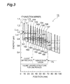
- Fig. 3 illustrates the quantum well structure and the subband level structure for part of the repeated structure of the multiples of the light emitting layer 17 and the injection layer 18 in the active layer 15.
- the device structure illustrated in Figs. 1 and 3 can be formed through crystal growth by molecular beam epitaxy (MBE) or metalorganic vapor phase epitaxy (MOVPE).
- the active layer 15 includes 40 periods of the unit layered structure 16 consisting of the quantum well light emitting layer 17 and the electron injection layer 18.
- the structure of the unit layered structure 16 for one period is a quantum well structure in which 11 of the quantum well layers 161 to 164 and 181 to 187 and 11 of the quantum barrier layers 171 to 174 and 191 to 197 are alternately stacked as illustrated in Fig. 3 .
- the quantum well layers are made of In 0.53 Ga 0.47 As layers.
- the quantum barrier layers are made of Al 0.52 In 0.48 As layers.
- the structure of the active layer 15 is thus an InGaAs/InAlAs structure lattice-matched to the InP substrate 50.
- the first quantum barrier layer 171 is positioned between the injection layer of the previous period and the light emitting layer 17 and functions as an injection barrier layer for an electron from the injection layer of the previous period into the light emitting layer 17.
- the unit layered structure 16 has the subband level structure illustrated in Fig. 3 that has the first light emission upper level (level 3) L up1 , the second light emission upper level (level 4) L up2 , the light emission lower levels (levels 2) L low , and the relaxation levels L r (level 1).
- the level structure in Fig. 3 has 12 levels contributing laser operation, of which a plurality of levels correspond to the light emission lower levels L low and the relaxation levels L r .
- the light emission lower levels and the relaxation levels form the miniband MB of a plurality of levels extending from the light emitting layer 17 to the injection layer 18.
- the thicknesses of the well layers and the barrier layers in the light emitting layer 17 and the injection layer 18 are quantum mechanically designed.
- the following describes a specific procedure of designing the quantum well structure of the unit layered structure 16.
- the energy difference between the first light emission upper level (level 3) L up1 and the light emission lower levels (level 2) L low , and the configuration of extracting an electron from the light emission lower levels are determined to give the oscillation wavelength of the laser device.
- the subband level structure described above has the lower miniband consisting a plurality of levels as the light emission lower levels L low .
- the energy difference between the first light emission upper level L up1 and the lower miniband including the light emission lower levels L low is determined by the well widths of the well layers 161 to 164 in the light emitting layer 17, the thicknesses of the barrier layers 172 to 174 in the light emitting layer 17, and the operational electric field.
- the operational electric field is set based on the expected layer thickness and voltage drop of the layered structure for one period. In the present configuration example, as described above, the operational electric field is set to 41 kV/cm.
- the well widths of the well layers 161 to 164, the thicknesses of the barrier layers 172 to 174, and the thickness of the barrier layer 191 of the injection layer 18, which determine the emission wavelength, cannot be determined independently. This is because the wave functions of the levels are sensitively affected by the quantum well layers and the barrier layers. For these semiconductor layers, their thicknesses are quantum mechanically determined through numerical calculation.
- the design wavelength will change at the next design step of determining the level position of the second light emission upper level L up2 , and thus the configuration of the quantum well layers 162 to 164 and the barrier layers 173 and 174 is roughly determined here.
- the well width of the quantum well layer 161 is then determined to set the second light emission upper level (level 4) L up2 .
- the thickness of the well layer 161 as the first well layer of the light emitting layer 17 is naturally smaller than those of the other well layers of the light emitting layer 17 because the ground level of the first well layer 161 as a single quantum well layer corresponds to the second light emission upper level L up2 .
- the first light emission upper level L up1 and the second light emission upper level L up2 need to have their wave functions coupled and overlapped sufficiently in the presence of the operational electric filed.
- the thickness of the first well layer 161 is thus set for the ground level of the well layer 161 and the first light emission upper level L up1 to have substantially the same energy in the presence of the operational electric field.
- the first light emission upper level L up1 is an excited level of the well layers other than the first well layer 161.
- the thickness of the second barrier layer 172 determines the size of anticrossing when the first light emission upper level L up1 and the second light emission upper level L up2 are coupled (the energy difference ⁇ E 43 between the level 3 and the level 4 when the levels are completely coupled).
- the size of anticrossing is large for the thin barrier layer 172 and small for the thick barrier layer 172.
- the thickness of the barrier 172 needs to be appropriately set smaller than that of the injection barrier layer 171. In the configuration example illustrated in Fig. 4 , the thickness of the barrier layer 172 is set to 2.7 nm to set the energy difference ⁇ E 43 between the light emission upper levels L up1 and L up2 to 18 meV.
- the levels existing in the electron injection layer 18 are also used as levels included in the miniband MB, and thus the thickness of the first barrier layer (exit barrier layer) 191 of the injection layer 18 needs to be set small to allow the wave functions of these levels to leak into the light emitting layer 17.
- the exit barrier layer 191 needs to be carefully designed because its too large thickness would not only deteriorate electron flow from the light emitting layer 17 to the injection layer 18 but also prevent formation of the lower miniband MB. In the present configuration example, as described above, the first barrier layer 191 does not function as an effective exit barrier.
- the design wavelength and the separation between the levels keep changing, but every time when a change happens a fine adjustment is carried out to eventually determine all the thicknesses of the quantum well layers and the barrier layers in the light emitting layer 17.
- the thicknesses of the well layers 161 to 164 are set to 3.1 nm, 7.5 nm, 5.8 nm, and 5.2 nm, respectively.
- the thicknesses of the barrier layers 172 to 174 and the barrier layer 191 of the injection layer 18 are set to 2.7 nm, 0.9 nm, 1.0 nm, and 1.2 nm, respectively.
- the electron injection layer 18 is designed below.
- a funnel injector Patent Literature 8: Japanese Patent Application Laid-Open Publication No. 10-4242 .
- the energy differences of the miniband MB can be narrowed toward the subsequent period, thereby enhancing the injection efficiency of an electron into the second light emission upper level L up2 .
- This level structure can be achieved by making the thicknesses of the quantum well layers smaller and the thicknesses of the barrier layers larger in the injection layer 18 from the light emitting layer 17 side toward the light emitting layer 17b of the subsequent period.
- the design needs to start with the quantum well layer 187 adjacent to the light emitting layer 17b of the subsequent period. This is because the wave function of the level existing in the well layer 187 (the ground level in the injection layer 18 in the presence of the operational electric field) needs to be configured to follow that of the light emission upper level under any electric field lower than the operational electric field.
- the relaxation levels in the well layer 187 are not only lower than the second light emission upper level L up2 in the well layer 161 but also lower than the first light emission upper level L up1 .
- the electric field becomes close to the operational electric field, an electron is first injected into the first light emission upper level L up1 , which makes it difficult to have a wide FWHM of light emission.
- the thicknesses of the other quantum well layers and the barrier layers in the injection layer 18 are determined by the same method conventionally done.
- the thickness of the first barrier layer 191 of the injection layer 18 is set as described above.
- the thicknesses of the well layers and the barrier layers on the exit barrier layer 191 side are designed accordingly to enable transporting of all electrons from the levels existing in the light emitting layer 17 to the miniband in the injection layer 18.
- the relaxation miniband needs to be narrowed sufficiently to allow electrons from the injection layer 18 to be injected into the second light emission upper level L up2 of the subsequent period but not into the level L h on a higher energy side.
- the thicknesses of the well layers 181 to 187 are set to 4.1 nm, 3.8 nm, 3.5 nm, 3.4 nm, 3.4 nm, 3.4 nm, and 3.3 nm, respectively.
- the thicknesses of the barrier layers 192 to 197 are set to 1.5 nm, 1.6 nm, 1.7 nm, 2.0 nm, 2.3 nm, and 2.8 nm, respectively.
- the barrier layer 171 determines the coupling strength between the periods in the cascade structure of the unit layered structures 16 and determines the maximum current to flow.
- the coupling strength between the wave functions is determined by the anticrossing gap, and in the present configuration example the anticrossing gap is designed to be 7.3 meV to allow an equivalent current to the conventional technology to flow.
- the thickness of the injection barrier layer 171 thus designed is 3.7 nm.
- Fig. 5 is a graph illustrating the operational voltage dependency of an emission spectrum obtained with the QCL.
- the abscissa represents the emission energy (meV) and the ordinate represents the emission intensity (a.u.).
- Graphs A1 to A7 represent the emission spectra at applied voltages of 5.9 V, 6.8 V, 7.6 V, 8.3 V, 9.0 V, 9.7 V, and 10.3 V, respectively.
- Graphs A1 to A7 by adopting the level structure described above (dual-state-to-continuum structure) in the active layer, its emission spectrum exhibits a wide and flat emission.
- the FWHM of light emission in this case is equivalent to that of a two-stack bound-to-continuum (BTC) structure, and a wide and high quality emission is achieved by a single design recipe.
- BTC two-stack bound-to-continuum
- Fig. 6 is a graph illustrating the voltage dependency of the FWHM of light emission (FWHM of the emission spectrum).
- the abscissa represents the applied voltage (V) and the ordinate represents the FWHM (meV), which is the full width half maximum.
- the graphs represent operational examples at an operational temperatures of 300 K (Graph B1) and 303 K (Graphs B2 and B3).
- Graphs (data plots) B1 to B3 illustrate the voltage dependencies of the FWHM of light emission when the novel structure described above, the conventional bound-to-bound structure, and the BTC structure are adopted respectively.
- Graphs B1 to B3 a markedly large FWHM of light emission is obtained for the novel structure described above as compared to the other structures.
- the voltage dependency of the FWHM of light emission shows that the FWHM of light emission decreases for the BTC structure as the voltage increases.
- the FWHM of light emission is substantially constant for the novel structure and the voltage dependency is significantly small. This suggests that the novel structure described above has a markedly high superiority in being adopted in laser devices such as DFB type and EC type.
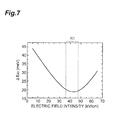
- Fig. 7 is a graph illustrating the electric field intensity dependency of the energy difference between the first light emission upper level L up1 and the second light emission upper level L up2 .
- the abscissa represents the electric field intensity (kV/cm) applied to the active layer 15, and the ordinate represents the energy difference ⁇ E 43 (meV) between the first light emission upper level and the second light emission upper level.
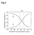
- Fig. 8 is a graph illustrating the electric field intensity dependency of the existence probability of an electron at the first light emission upper level L up1 and at the second light emission upper level L up2 in the light emitting layer 17 except for the first well layer 161 therein.
- the abscissa represents the electric field intensity (kV/cm) and the ordinate represents the existence probability of an electron at the light emission upper level except for the first well layer 161.
- Graph C1 represents the existence probability of the first light emission upper level except for the first well layer 161
- Graph C2 represents the existence probability of the second light emission upper level except for the first well layer 161.
- Ranges R1 and R2 in Figs. 7 and 8 which are the ranges of electric field intensity of 36 to 47 kV/cm
- the first light emission upper level L up1 and the second light emission upper level L up2 are strongly coupled and the existence probability of an electron except for the first well layer 161 is more than 30% for the first light emission upper level L up1 and the second light emission upper level L up2 , a preferable condition fulfilled. In this condition, the energy difference between the two light emission upper levels reaches its minimum.
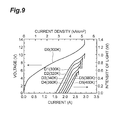
- the following further describes the characteristics and other specifications of the QCL according to the configuration example above with reference to Figs. 9 to 11 .
- the characteristics are described for the laser device having a configuration in which the resonator has a length of 4 mm and a ridge has a width of 14 ⁇ m in the ridge waveguide configuration.
- a laser end face of the laser device is formed by cleavage and has no coating or the like applied.
- the threshold current density is as low as 2.6 kA/cm 2 at room temperature, which is a value comparable to that of a laser device with a narrow gain width.
- the total light emission from the both end faces reaches as high as 1 W at room temperature, demonstrating that a markedly high outputting laser device is feasible.
- the slope efficiency is obtained to be approximately 1 W/A.
- Fig. 11 is a graph of an oscillation spectrum of the QCL.
- the abscissa represents the wavenumber (cm -1 ) and the ordinate represents the intensity (a.u.).
- Graphs E1 to E3 represents the oscillation spectra at a current of 1.75 A, 2.3 A, and 2.7 A, respectively.
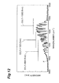
- Fig. 12 is a graph of the oscillation spectrum of the QCL and the single mode oscillation according to the periodicity of each diffraction grating.
- the abscissa represents the wavenumber (cm -1 ) and the ordinate represents the intensity (a.u.).
- the single mode oscillation is obtained in a wide range of wavelength over 100 cm -1 approximately with the same wafer in the QCL 1 according to the present embodiment. This suggests that for a determined period of the diffraction grating, the gain of the QCL may shift to the short wavelength side or the long wavelength side, but the single mode oscillation is still obtained stably at a single wavelength.
- the QCLs that perform a plurality of kinds of single mode oscillation can be fabricated from a single wafer.
- the asperity shape of the first groove pattern P1 is substantially identical to the asperity shape of a third groove pattern P3 and the asperity shape of the phase shifting diffraction grating to be made.
- the protrusion positioned in the vicinity of the center in the width direction of the first groove pattern P1 has the width set about twice as those of the other protrusions.
- An electron e - from the level L r in the injection layer 18a of the previous period into the quantum well light emitting layer 17 is preferably injected into the second light emission upper level L up2 .
- the second light emission upper level which is the higher level between the first light emission upper level and the second light emission upper level
- carriers are distributed evenly between the two upper levels, thereby appropriately achieving light emitting transitions from the first light emission upper level and the second light emission upper level to the lower levels.
- the resin stamper 201 is made of the resin film 200 having flexibility, and a plurality of diffraction gratings can be made at once on the wafer for the resin stamper 201 with a large area. This can improve the mass production capacity of the QCL 1.
- a plurality of diffraction gratings with different periods can be made at once on the wafer according to the second groove pattern P2 of the resin stamper 201.
- the QCL 1 capable of performing a plurality of kinds of single mode oscillation can be made from one wafer.
- the diffraction grating formed on the surface of the wafer is a phase shifting diffraction grating.
- the bimodal oscillation stemming from an error in the position of cleavage of the diffraction grating in manufacturing is thus prevented, which allows manufacturing of the QCL 1 that stably performs the single mode oscillation.
- a ⁇ /4 phase shifting diffraction grating with the asperity phase of the diffraction grating inverted in the vicinity of the center of the diffraction grating is preferably adopted in the present embodiment in particular, and thus the oscillation threshold gain can be only for one mode, the minimum mode.
- the InP film 301 and the InGaAs film 302 are formed on the intermediate structure 300 in order closest to the active layer 15.
- the distance from the active layer 15 to the InGaAs film 302 can thus be adjusted through the thickness of the InP film 301.
- the InGaAs film 302 is etched to function as a diffraction grating, and thus the coupling factor of the diffraction grating can be adjusted for a wavelength by adjusting the thickness of the InP film 301 as the base 20a.
- the InP film 301 functions as a stopper during etching of the InGaAs film 302, thereby allowing a markedly precise control of the groove depth of the diffraction grating.
- the resist film 304 is formed of ultraviolet curable resin, and the resin stamper 201 has ultraviolet transparency. While the resin stamper 201 is press-bonded to the resist film 304, ultraviolet light can thus be applied through the resin stamper 201 to the resist film 304.
- the InP substrate 100 is used as the mother stamper 103, but other materials or other processing methods may be selected as long as precise processing is possible.
Landscapes
- Engineering & Computer Science (AREA)
- Physics & Mathematics (AREA)
- Chemical & Material Sciences (AREA)
- Nanotechnology (AREA)
- Optics & Photonics (AREA)
- Crystallography & Structural Chemistry (AREA)
- Electromagnetism (AREA)
- General Physics & Mathematics (AREA)
- Condensed Matter Physics & Semiconductors (AREA)
- Theoretical Computer Science (AREA)
- Mathematical Physics (AREA)
- Manufacturing & Machinery (AREA)
- Life Sciences & Earth Sciences (AREA)
- Biophysics (AREA)
- Plasma & Fusion (AREA)
- Semiconductor Lasers (AREA)
- Photosensitive Polymer And Photoresist Processing (AREA)
Abstract
Description
- The present invention relates to a quantum cascade laser manufacturing method.
- Light in a mid-infrared wavelength range (wavelength of 5 µm to 30 µm, for example) is important in the field of spectroscopic analysis. In recent years, a quantum cascade laser (QCL) has been popular as a high performance semiconductor light source operating in the wavelength range (refer to
Patent Literatures 1 to 8 and Non-PatentLiteratures 1 to 9, for example). - The QCL is a unipolar laser utilizing a subband level structure formed in a semiconductor well structure to generate light through intersubband electron transition. The QCL has a cascade connection of a plurality of quantum well light emitting layers each having a quantum well structure that form an active region, thereby achieving high efficient and high output performance. The cascade connection of the quantum well light emitting layers is implemented by alternately stacking the quantum well light emitting layer and an electron injection layer, using the injection layer for injecting an electron into a light emission upper level.
-
- [Patent Literature 1]
U.S. Patent No. 5,457,709 - [Patent Literature 2]
U.S. Patent No. 5,745,516 - [Patent Literature 3]
U.S. Patent No. 6,751,244 - [Patent Literature 4]
U.S. Patent No. 6,922,427 - [Patent Literature 5] Japanese Patent Application Laid-Open Publication No.
8-279647 - [Patent Literature 6] Japanese Patent Application Laid-Open Publication No.
2008-177366 - [Patent Literature 7] Japanese Patent Application Laid-Open Publication No.
2008-60396 - [Patent Literature 8] Japanese Patent Application Laid-Open Publication No.
10-4242 -
- [Non Patent Literature 1] M.Beck et al., "Continuous Wave Operation of a Mid-Infrared Semiconductor Laser at Room Temperature", Science Vol.295 (2002), pp.301-305
- [Non Patent Literature 2] J. S.Yu et al., "High-Power Continuous-Wave Operation of a 6µm Quantum-Cascade Laser at Room Temperature", Appl. Phys. Lett.Vol.83 (2003), pp.2503-2505
- [Non Patent Literature 3] A.Evans et al., "Continuous-Wave Operation of λ∼4.8 µm Quantum-Cascade Lasers at Room Temperature", Appl. Phys. Lett. Vol. 85 (2004), pp.2166-2168
- [Non Patent Literature 4] A.Tredicucci et al., "A Multiwavelength Semiconductor Laser", Nature Vol. 396 (1998), pp.350-353
- [Non Patent Literature 5] A.Wittmann et al., "Heterogeneous High-Performance Quantum-Cascade Laser Sources for Broad-Band Tuning", IEEE J. Quantum Electron. Vol. 44 (2008), pp.1083-1088
- [Non Patent Literature 6] A.Wittmann et al., "High-Performance Bound-To-Continuum Quantum-Cascade Lasers for Broad-Gain Applications", IEEE J. Quantum Electron. Vol.44 (2008), pp.36-40
- [Non Patent Literature 7] R.Maulini et al., "Broadband Tuning of External Cavity Bound-to-Continuum Quantum-Cascade Lasers", Appl. Phys. Lett. Vol.84 (2004), pp.1659-1661
- [Non Patent Literature 8] A.Wittmann et al., "Intersubband Linewidths in Quantum Cascade Laser Designs", Appl. Phys. Lett. Vol.93 (2008), pp.141103-1-141103-3
- [Non Patent Literature 9] Claire Gmachl et al., "Complex-Coupled Quantum Cascade Distributed-Feedback Laser", IEEE Photon.Technol. Lett., Vol.9 (1997), pp.1090-1092
- In the QCL described above, the operation temperature of the device had been limited to extremely low temperatures when the QCL initially had succeeded in laser oscillation, although in 2002 M. Beck et al. achieved room temperature continuous wave (CW) operation at an oscillation wavelength of 9.1 µm (Non Patent Literature 1). After that, the room temperature CW operation was also achieved by M. Razeghi and his team at oscillation wavelengths of 6 µm and 4.8 µm (
Non Patent Literatures 2 and 3). Nowadays the room temperature continuous oscillation has achieved in a wide range of wavelengths of 3.8 to 11.5 µm and reached at the stage of putting into practical use. - Following this successful room temperature continuous oscillation, efforts have been made to develop a QCL capable of single mode oscillation in a wide range of wavelengths by means of using a laser device with an external cavity (EC). Development has also been made for a distributed feedback (DFB) QCL capable of room temperature CW operation and scanning a single wavelength (refer to
Non Patent Literature 9, for example). - In the conventional DFB QCL, device characteristics have been improved by concentrating the gain of light emission with a structure of generating light through electron intersubband transition from one light emission upper level into one light emission lower level (
Patent Literature 6, for example). Specifically, such a structure allows laser operation to achieve a low threshold, high slope efficiency, and the room temperature CW operation. - In some cases, however, bimodal oscillation at both ends of a stop band occurs stemming from an error in the position of cleavage of the diffraction grating in manufacturing, which affects the yield. It has thus been desired to precisely manufacture the diffraction grating.
- An objective of the present invention is thus to provide a method of manufacturing a QCL including a high-precision diffraction grating and capable of stably performing single mode oscillation.
- A QCL manufacturing method according to an aspect of the present invention includes: a first step of preparing a mother stamper with a predetermined first groove pattern formed on a surface of a substrate; a second step of pressing the mother stamper against a resin film having flexibility to transfer the first groove pattern to the resin film and making a resin stamper with a second groove pattern formed on the resin film, the second groove pattern having an inverted asperity of the first groove pattern; a third step of making a wafer with an active layer formed on a semiconductor substrate, the active layer having a cascade structure in which a unit layered structure including a quantum well light emitting layer and an injection layer is stacked in multiples to alternately stack the quantum well light emitting layer and the injection layer; a fourth step of forming a resist film on a surface on the active layer side of the wafer; a fifth step of pressing the resin stamper against the resist film by air pressure to transfer the second groove pattern to the resist film and forming on the resist film a third groove pattern having an inverted asperity of the second groove pattern; and a sixth step of etching the wafer with the resist film serving as a mask to form a diffraction grating on a surface of the wafer.
- A wafer for a QCL is typically a layered structure of a compound semiconductor. Its mechanical strength is thus not so high and its surface flatness is also unsatisfactory (the maximum of about 10 µm roughness in the wafer surface). In the QCL manufacturing method according to an aspect of the present invention, the resin stamper made of the resin film having flexibility is pressed against the resist film by air pressure to transfer the second groove pattern to the resist film. The wafer with low flatness is thus evenly pressured by the air pressure, whereby the second groove pattern of the resin stamper is transferred to the resist film markedly precisely. Accordingly, a high-precision diffraction grating is obtained, which allows manufacturing of the QCL capable of stably performing single mode oscillation.
- In the QCL manufacturing method according to an aspect of the present invention, the mother stamper with the first groove pattern formed is pressed against the resin film to transfer the first groove pattern to the resin film, thereby making the resin stamper with the second groove pattern formed on the resin film, the second groove pattern having the inverted asperity of the first groove pattern. With the mother stamper made once, any number of the same resin stampers can be duplicated in a case of the resin stamper being damaged. The resin stamper can be used any number of times as long as it is not damaged.
- In the QCL manufacturing method according to an aspect of the present invention, the resin stamper is made of the resin film having flexibility, and a plurality of diffraction gratings can be made at once on the wafer for the resin stamper with a large area. This can improve the mass production capacity of the QCL. A plurality of diffraction gratings with different periods can be made at once on the wafer depending on the second groove pattern of the resin stamper. The QCL capable of performing a plurality of kinds of single mode oscillation can be made from one wafer.
- The diffraction grating formed on the surface of the wafer in the sixth step may be a phase shifting diffraction grating. Such a configuration prevents bimodal oscillation stemming from an error in the position of cleavage of the diffraction grating in manufacturing, which allows manufacturing of the QCL that stably performs single mode oscillation. A λ/4 phase shifting diffraction grating with the asperity phase of the diffraction grating inverted in the vicinity of the center of the diffraction grating is preferably adopted in particular, because the oscillation threshold gain is then only for one mode, the minimum mode.
- After the third step and before the fourth step, another step may be included to form an intermediate film on the surface on the active layer side of the wafer. By selecting as the intermediate film a material giving the adhesion between the wafer and the resist film, a rip-off (a phenomenon in which part of the third pattern is flaked off when the resin stamper is released from the resist film because of the adhesion between the resin stamper and part of the resist film) can be reduced. SiN or SiO2 can be selected as a material of the intermediate film, for example.
- An InP film and an InGaAs film may be formed on the active layer side of the wafer in order closest to the active layer. With this configuration, the distance from the active layer to the InGaAs film can be adjusted through the thickness of the InP film. The InGaAs film is etched to function as a diffraction grating, and thus the coupling factor of the diffraction grating can be adjusted for a wavelength by adjusting the thickness of the InP film as a base. The InP film functions as a stopper during etching of the InGaAs film, thereby allowing a markedly precise control of the groove depth of the diffraction grating.
- The resist film may be formed of ultraviolet curable resin and the resin stamper may have ultraviolet transparency. With this configuration, while the resin stamper is press-bonded to the resist film, ultraviolet light can be applied through the resin stamper to the resist film.
- The present invention provides a method of manufacturing a QCL including a high-precision diffraction grating and capable of stably performing single mode oscillation.
-
- [
Fig. 1] Fig. 1 is a diagram illustrating the configuration of a QCL according to an embodiment of the present invention. - [
Fig. 2] Fig. 2 is a diagram illustrating a subband level structure of an active layer of the QCL. - [
Fig. 3]Fig. 3 is a diagram illustrating an example of the configuration of a unit layered structure included in the active layer. - [
Fig. 4]Fig. 4 is a table for an example configuration of the unit layered structure for one period in the active layer. - [
Fig. 5] Fig. 5 is a graph of an emission spectrum obtained with the QCL. - [
Fig. 6] Fig. 6 is a graph illustrating the voltage dependency of a full width at half maximum of light emission. - [
Fig. 7] Fig. 7 is a graph illustrating the electric field intensity dependency of the energy difference between a first light emission upper level and a second light emission upper level. - [
Fig. 8] Fig. 8 is a graph illustrating the electric field intensity dependency of the existence probability of an electron at the first light emission upper level or at the second light emission upper level in the light emitting layer except for a first well layer therein. - [
Fig. 9] Fig. 9 is a graph illustrating the current-voltage-light output characteristics of the QCL. - [
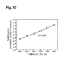
Fig. 10] Fig. 10 is a graph illustrating the temperature dependency of threshold current density. - [
Fig. 11] Fig. 11 is a graph of an oscillation spectrum of the QCL. - [
Fig. 12] Fig. 12 is a graph of the oscillation spectrum of the QCL and single mode oscillation corresponding to the periodicity of each diffraction grating. - [
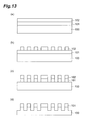
Fig. 13] Fig. 13 is a diagram illustrating the process of making a mother stamper and a resin stamper. - [
Fig. 14] Fig. 14 is a diagram illustrating the process of making the mother stamper and the resin stamper. - [
Fig. 15] Fig. 15 is a graph of temperature and pressure against time in making the resin stamper. - [
Fig. 16] Fig. 16 is a diagram illustrating the process of making a phase shifting diffraction grating. - [
Fig. 17] Fig. 17 is diagram illustrating the process of making the phase shifting diffraction grating. - [
Fig. 18] Fig. 18 is a graph of temperature and pressure against time in making the phase shift diffraction grating. - The following describes preferred embodiments of the present invention with reference to the accompanying drawings. The same numeral denotes the same element or an element having the same function, and any redundant description will be omitted.
- A
QCL 1 according to the present embodiment is a unipolar laser device that generates light through intersubband electron transition in a semiconductor quantum well structure. TheQCL 1 has a configuration in which acladding layer 13 a, alower core layer 11, anactive layer 15, anupper core layer 12, adiffraction grating layer 20, acladding layer 13b, and acontact layer 14 are sequentially stacked on asemiconductor substrate 10 in this order from thesemiconductor substrate 10 side as illustrated inFig. 1 . - The
active layer 15 has a cascade structure in which a quantum well light emitting layer used for generating light and an electron injection layer used for injecting an electron into the light emitting layer are alternately stacked in multiples. A semiconductor layered structure including the quantum well light emitting layer and the injection layer is taken as a unit layeredstructure 16 for one period, and the unit layeredstructure 16 is stacked in multiples to construct theactive layer 15 having a cascade structure. The number of stacks of the unit layeredstructures 16 including the quantum well light emission layer and the injection layer is set as appropriate, for example, in the hundreds. Theactive layer 15 is disposed on thesemiconductor substrate 10 through thelower core layer 11 in the present embodiment, but may be disposed directly on thesemiconductor substrate 10. - Each of the unit layered
structures 16 included in theactive layer 15 includes the quantum well light emittinglayer 17 and theelectron injection layer 18 as illustrated inFig. 2 . Thelight emitting layer 17 and theinjection layer 18 each have a certain quantum well structure including a quantum well layer and a quantum barrier layer. This configuration forms a subband level structure that is an energy level structure due to a quantum well structure in the unit layeredstructure 16. - The subband level structure formed in the unit layered
structure 16 includes a first light emission upper level (level 3) Lup1, a second light emission upper level (level 4) Lup2, and a plurality of light emission lower levels (levels 2) Llow as illustrated inFig. 2 . The second light emission upper level Lup2 has a higher energy than the first light emission upper level Lup1. The light emission lower levels Llow have lower energies than the first light emission upper level Lup1. - The
light emitting layer 17 includes n (n is an integer equal to or greater than two) well layers. One of the first light emission upper level Lup1 and the second light emission upper level Lup2 is a level attributable to the ground level of the first well layer on aninjection layer 18a side of the first period, and the other is a level attributable to an excited level of the well layers except for the first well layer (the second to the n-th well layers). - The energy difference ΔE43 between the first light emission upper level Lup1 and the second light emission upper level Lup2 is set to be smaller than the energy ELO of the longitudinal optical (LO) phonon (ΔE43<ELO). A high energy level (level 5) Lh is adjacent to and higher than the second light emission upper level Lup2. The energy difference ΔE54 between the second light emission upper level Lup2 and the high energy level Lh is set to be larger than the energy ELO of the LO phonon (ELO<ΔE54).
- The energy ELO of the LO phonon is, for example, 34 meV for InGaAs as the semiconductor material of the quantum well layer. The energy ELO of the LO phonon is 36 meV for the quantum well layer of GaAs and 32 meV for the quantum well layer of InAs, the energies approximately equal to 34 meV described above.
- The two light emission upper levels Lup1 and Lup2 are preferably designed so that the energies of the levels are equal and their wave functions are strongly coupled (anticrossing) in the presence of an operational electric field. With this configuration, these two upper levels behave as if they are a single light emission upper level having a range in energies. By controlling the coupling strength between the two upper levels, it is possible to control the full width at half maximum (FWHM) of light emission. The light emission lower levels Llow constitute a lower miniband MB including a plurality of levels, and a light emitting transition from the first light emission upper level and the second light emission upper level disperses to the lower miniband.
- The unit layered
structure 16 illustrated inFig. 2 includes an injection barrier layer provided between the light emittinglayer 17 and theinjection layer 18a of the unit layered structure of the previous period. The injection barrier layer is an injection barrier for an electron injected from theinjection layer 18a into thelight emitting layer 17. An exit barrier layer may be provided between the light emittinglayer 17 and theinjection layer 18. The exit barrier layer is an exit barrier for an electron from thelight emitting layer 17 into theinjection layer 18.Fig. 2 illustrates a configuration in which simply a thin barrier layer is provided between the light emittinglayer 17 and theinjection layer 18, thin enough to allow the wave function to leak through it sufficiently. - The miniband MB has a band structure with a plurality of levels extending from the
light emitting layer 17 to theinjection layer 18, the band structure resulting from the coupling between the miniband in the quantum well light emittinglayer 17 and the miniband in theinjection layer 18. Of the miniband MB, the higher energy portion in thelight emitting layer 17 functions as the lower miniband consisting of the light emission lower levels Llow described above, whereas the lower energy portion in theinjection layer 18 functions as a relaxation miniband including a relaxation level (level 1) Lr that allows an electron having undergone a light emitting transition to be relaxed from the light emission lower levels Llow into alight emitting layer 17b of the subsequent period. - The light emission lower levels Llow and the relaxation level Lr, which are continuous levels, allow a markedly high efficient generation of the population inversion. The ground level Lg in the
injection layer 18 among the relaxation levels Lr constituting the relaxation miniband is preferably designed to strongly couple with the second light emission upper level Lup2 in thelight emitting layer 17b of the unit layered structure of the subsequent period in the presence of an operational electric field. - An electron e- at the relaxation level Lr in the
injection layer 18a of the previous period is injected into thelight emitting layer 17 through the injection barrier owing to the resonant tunneling effect. This markedly strongly populates the second light emission upper level Lup2 coupled with the relaxation level Lr. At the same time, the first light emission upper level Lup1 is supplied with sufficient electrons through a fast scattering process such as an electron-electron scattering, and thus the two light emission upper levels Lup1 and Lup2 are supplied with sufficient carriers. - Electrons injected into the first light emission upper level Lup1 and the second light emission upper level Lup2 transit to the light emission lower levels Llow constituting the lower miniband. Through this, light hv having the wavelength corresponding to the energy difference between the upper levels Lup1 and Lup2 and the lower levels Llow is generated and emitted. As described above, the two upper levels behave as if they are a single light emission level having a range in energies, and thus the obtained light emitting spectrum is an evenly distributed spectrum.
Fig. 2 only illustrates a light emitting transition from the upper levels Lup1 and Lup2 to the highest lower level Llow and omits illustration of transitions to the other lower levels. - The electron transited to the light emission lower level Llow is then relaxed fast through interminiband relaxation by the LO phonon scattering, the electron-electron scattering, and other interactions within the miniband MB including the light emission lower levels Llow and the relaxation levels Lr in the
injection layer 18. Through such an extraction of a carrier from the light emission lower level Llow through interminiband relaxation, the population inversion to achieve laser oscillation is easily generated between the two upper levels Lup1 and Lup2 and the lower levels Llow. An electron relaxed from the light emission level Llow to the level Lr in theinjection layer 18 is injected via the ground level Lg in theinjection layer 18, which is a relaxation level on a lower energy side, to the light emission upper levels Lup1 and Lup2 in thelight emitting layer 17b of the subsequent period in a cascade manner. - Through repetition of the injection, the light emitting transition, and the relaxation in the unit layered
structures 16 included in theactive layer 15, light generation occurs in theactive layer 15 in a cascade manner. In other words, with large numbers of the quantum well light emittinglayers 17 and the injection layers 18 alternately stacked, an electron is allowed to move sequentially through thelayered structures 16 in a cascade manner and generates light h through intersubband transition in each of thelayered structures 16. Such light is resonated in an optical resonator to generate a laser light of a certain wavelength. - Back in
Fig. 1 , thediffraction grating layer 20 includes abase 20a disposed on theactive layer 15 through theupper core layer 12 and a plurality of protrusions 20b disposed on thebase 20a. Thebase layer 20a is formed on the entire surface of theupper core layer 12. Thebase layer 20a functions as an etching stopper when the protrusions 20b are fabricated by etching, and have a function of adjusting the distance from theactive layer 15 to the protrusions 20b. - The protrusions 20b are arranged mutually and equally separate to form a certain pattern on the
base 20a. When a target wavelength is 5.26 µm (wavenumber is 1901 cm-1), the pitch of the protrusions 20b can be set to 824 nm utilizing the first order diffraction. Aprotrusion 21 located about the center in the width direction of theQCL 1 has its width set to about twice as that of theother protrusions 22 as illustrated inFig. 1 . As a result of theprotrusions 21 thus functioning as a phase shifting portion, the protrusions 20b (the diffraction grating layer 20) function as a λ/4 phase shifting diffraction grating. Thecladding layer 13b is formed to fill the gaps between the protrusions 20b. - The protrusions 20b can be formed by nanoimprint lithography described in detail later. The gap (period) between the protrusions 20b is 824 nm approximately when the target wavelength is 5.26 µm (wavenumber is 1901 cm-1), for example, and the accuracy of manufacturing the diffraction grating is ±0.8 nm or less. The nanoimprint lithography enables highly accurate manufacturing of a phase shifting diffraction grating with a large area, thereby preventing the bimodal oscillation.
- The following describes a specific example of the structure of a device including the quantum well structure in the active layer with reference to
Figs. 1 ,3 , and4 . - The
semiconductor substrate 10 according to the present configuration example is made of an n-type InP single crystal. The cladding layers 13a and 13b are made of InP, and their thicknesses may be set to 3.5 µm approximately. Thelower core layer 11 is made of InGaAs, and its thickness may be set to 300 nm approximately. Theupper core layer 11 is made of InGaAs, and its thickness may be set to 300 nm approximately. Thecontact layer 14 is made of InGaAs, and its thickness may be set to 10 nm approximately. Thebase layer 20a is made of InP, and its thickness may be set to 200 nm to 300 nm approximately. The protrusions 20b are made of InGaAs, and their thickness may be set to 100 nm approximately. - The quantum well structure of the
active layer 15 according to the present configuration example has its oscillation wavelength set to 8.7 µm (oscillation energy: 142 meV) and the operational electric field set to 41 kV/cm, for example.Fig. 3 illustrates the quantum well structure and the subband level structure for part of the repeated structure of the multiples of thelight emitting layer 17 and theinjection layer 18 in theactive layer 15. The device structure illustrated inFigs. 1 and3 can be formed through crystal growth by molecular beam epitaxy (MBE) or metalorganic vapor phase epitaxy (MOVPE). - The
active layer 15 according to the present configuration example includes 40 periods of the unit layeredstructure 16 consisting of the quantum well light emittinglayer 17 and theelectron injection layer 18. The structure of the unit layeredstructure 16 for one period is a quantum well structure in which 11 of the quantum well layers 161 to 164 and 181 to 187 and 11 of the quantum barrier layers 171 to 174 and 191 to 197 are alternately stacked as illustrated inFig. 3 . - Among these semiconductor layers of the unit layered
structure 16, the quantum well layers are made of In0.53Ga0.47As layers. The quantum barrier layers are made of Al0.52In0.48As layers. The structure of theactive layer 15 is thus an InGaAs/InAlAs structure lattice-matched to theInP substrate 50. - As illustrated in
Fig. 3 , in the unit layeredstructure 16, a layered portion consisting of the fourwell layers 161 to 164 and the fourbarrier layers 171 to 174 mainly functions as thelight emitting layer 17. In the unit layeredstructure 16, a layered portion consisting of the sevenwell layers 181 to 187 and the sevenbarrier layers 191 to 197 mainly functions as theinjection layer 18. Among the semiconductor layers of thelight emitting layer 17, the firstquantum barrier layer 171 is positioned between the injection layer of the previous period and thelight emitting layer 17 and functions as an injection barrier layer for an electron from the injection layer of the previous period into thelight emitting layer 17. - In the present configuration example, the exit barrier layer is positioned between the light emitting
layer 17 and theinjection layer 18 but does not practically function as an exit barrier for an electron from thelight emitting layer 17 into theinjection layer 18. InFig. 3 , the wave functions of the light emission upper levels Lup1 and Lup2 decay before thefifth barrier layer 191 of the unit layeredstructure 16, which is practically taken as an exit barrier layer to functionally separate thelight emitting layer 17 and theinjection layer 18 before and after the exit barrier layer.Fig. 4 illustrates an example of the configuration of the unit layeredstructure 16 for one period in theactive layer 15. - The unit layered
structure 16 has the subband level structure illustrated inFig. 3 that has the first light emission upper level (level 3) Lup1, the second light emission upper level (level 4) Lup2, the light emission lower levels (levels 2) Llow, and the relaxation levels Lr (level 1). The level structure inFig. 3 has 12 levels contributing laser operation, of which a plurality of levels correspond to the light emission lower levels Llow and the relaxation levels Lr. As described above, the light emission lower levels and the relaxation levels form the miniband MB of a plurality of levels extending from thelight emitting layer 17 to theinjection layer 18. The thicknesses of the well layers and the barrier layers in thelight emitting layer 17 and theinjection layer 18 are quantum mechanically designed. - The following describes a specific procedure of designing the quantum well structure of the unit layered
structure 16. First, the energy difference between the first light emission upper level (level 3) Lup1 and the light emission lower levels (level 2) Llow, and the configuration of extracting an electron from the light emission lower levels are determined to give the oscillation wavelength of the laser device. The subband level structure described above has the lower miniband consisting a plurality of levels as the light emission lower levels Llow. - The energy difference between the first light emission upper level Lup1 and the lower miniband including the light emission lower levels Llow is determined by the well widths of the well layers 161 to 164 in the
light emitting layer 17, the thicknesses of the barrier layers 172 to 174 in thelight emitting layer 17, and the operational electric field. The operational electric field is set based on the expected layer thickness and voltage drop of the layered structure for one period. In the present configuration example, as described above, the operational electric field is set to 41 kV/cm. - The well widths of the well layers 161 to 164, the thicknesses of the barrier layers 172 to 174, and the thickness of the
barrier layer 191 of theinjection layer 18, which determine the emission wavelength, cannot be determined independently. This is because the wave functions of the levels are sensitively affected by the quantum well layers and the barrier layers. For these semiconductor layers, their thicknesses are quantum mechanically determined through numerical calculation. The design wavelength will change at the next design step of determining the level position of the second light emission upper level Lup2, and thus the configuration of the quantum well layers 162 to 164 and the barrier layers 173 and 174 is roughly determined here. - The well width of the
quantum well layer 161 is then determined to set the second light emission upper level (level 4) Lup2. The thickness of thewell layer 161 as the first well layer of thelight emitting layer 17 is naturally smaller than those of the other well layers of thelight emitting layer 17 because the ground level of thefirst well layer 161 as a single quantum well layer corresponds to the second light emission upper level Lup2. - The first light emission upper level Lup1 and the second light emission upper level Lup2 need to have their wave functions coupled and overlapped sufficiently in the presence of the operational electric filed. The thickness of the
first well layer 161 is thus set for the ground level of thewell layer 161 and the first light emission upper level Lup1 to have substantially the same energy in the presence of the operational electric field. In this case, the first light emission upper level Lup1 is an excited level of the well layers other than thefirst well layer 161. - The thickness of the
second barrier layer 172 determines the size of anticrossing when the first light emission upper level Lup1 and the second light emission upper level Lup2 are coupled (the energy difference ΔE43 between thelevel 3 and thelevel 4 when the levels are completely coupled). The size of anticrossing is large for thethin barrier layer 172 and small for thethick barrier layer 172. - The QCL according to an aspect of the present invention achieves a wide FWHM of light emission by controlling transition from the first light emission upper level Lup1 and the second light emission upper level Lup2 to the light emission lower levels Llow. Such function deteriorates for an inappropriate thickness of the
barrier layer 172. When thebarrier layer 172 is too thin, ΔE43 is large, which causes a transition to the light emission lower level Llow to be weighted in a transition to either of the first light emission upper level Lup1 and the second light emission upper level Lup2, resulting in a narrow FWHM of light emission. Even if light emission occurs without such weighting, its emission spectrum is nonuniform as in an interminiband transition. - In contrast, when the
barrier layer 172 is too thick, ΔE43 is too small. When there exists any barrier layer thicker than theinjection barrier layer 171 in the cascade structure, it is difficult to transport carriers, which may deteriorate the laser operation. With these considerations, the thickness of thebarrier 172 needs to be appropriately set smaller than that of theinjection barrier layer 171. In the configuration example illustrated inFig. 4 , the thickness of thebarrier layer 172 is set to 2.7 nm to set the energy difference ΔE43 between the light emission upper levels Lup1 and Lup2 to 18 meV. - As described above, the miniband MB serves as the light emission lower levels Llow. In the miniband MB, there are a number of levels with their wave functions extending in space. To achieve such a configuration, all the barrier layers included in the
light emitting layer 17 need to have a thin thickness, thereby strongly coupling their levels. - The levels existing in the
electron injection layer 18 are also used as levels included in the miniband MB, and thus the thickness of the first barrier layer (exit barrier layer) 191 of theinjection layer 18 needs to be set small to allow the wave functions of these levels to leak into thelight emitting layer 17. Theexit barrier layer 191 needs to be carefully designed because its too large thickness would not only deteriorate electron flow from thelight emitting layer 17 to theinjection layer 18 but also prevent formation of the lower miniband MB. In the present configuration example, as described above, thefirst barrier layer 191 does not function as an effective exit barrier. - In the process of designing the quantum well structure, the design wavelength and the separation between the levels keep changing, but every time when a change happens a fine adjustment is carried out to eventually determine all the thicknesses of the quantum well layers and the barrier layers in the
light emitting layer 17. As a result, the thicknesses of the well layers 161 to 164 are set to 3.1 nm, 7.5 nm, 5.8 nm, and 5.2 nm, respectively. The thicknesses of the barrier layers 172 to 174 and thebarrier layer 191 of theinjection layer 18 are set to 2.7 nm, 0.9 nm, 1.0 nm, and 1.2 nm, respectively. - The
electron injection layer 18 is designed below. In the present configuration example, a funnel injector (Patent Literature 8:Japanese Patent Application Laid-Open Publication No. 10-4242 injection layer 18. By employing the funnel injector, the energy differences of the miniband MB can be narrowed toward the subsequent period, thereby enhancing the injection efficiency of an electron into the second light emission upper level Lup2. This level structure can be achieved by making the thicknesses of the quantum well layers smaller and the thicknesses of the barrier layers larger in theinjection layer 18 from thelight emitting layer 17 side toward thelight emitting layer 17b of the subsequent period. - In designing the
injection layer 18 illustrated inFig. 3 , the design needs to start with thequantum well layer 187 adjacent to thelight emitting layer 17b of the subsequent period. This is because the wave function of the level existing in the well layer 187 (the ground level in theinjection layer 18 in the presence of the operational electric field) needs to be configured to follow that of the light emission upper level under any electric field lower than the operational electric field. - To achieve such a configuration, the thickness of the
well layer 187 needs to be slightly (a several angstrom) larger than that of thewell layer 161. In the present configuration example, for the thickness of thewell layer 161 of thelight emitting layer 17 set to 3.1 nm, the thickness of thewell layer 187 of theinjection layer 18 is set to 3.3 nm. This enables excitation of the second light emission upper level Lup2 through electron injection from the relaxation miniband, thereby achieving a wide FWHM of light emission. - The following considers a case where the
well layer 187 is thicker than thewell layer 161 by 6 A (0.6 nm, two atomic layer). In the presence of a low electric field, the relaxation levels in thewell layer 187 are not only lower than the second light emission upper level Lup2 in thewell layer 161 but also lower than the first light emission upper level Lup1. In such a level structure, when the electric field becomes close to the operational electric field, an electron is first injected into the first light emission upper level Lup1, which makes it difficult to have a wide FWHM of light emission. - After the thickness of the
well layer 187 is determined, the thicknesses of the other quantum well layers and the barrier layers in theinjection layer 18 are determined by the same method conventionally done. The thickness of thefirst barrier layer 191 of theinjection layer 18 is set as described above. - Among the semiconductor layers included in the
injection layer 18, the thicknesses of the well layers and the barrier layers on theexit barrier layer 191 side are designed accordingly to enable transporting of all electrons from the levels existing in thelight emitting layer 17 to the miniband in theinjection layer 18. In contrast, for the thicknesses of the well layers and the barrier layers on theinjection barrier layer 171 of the subsequent period, the relaxation miniband needs to be narrowed sufficiently to allow electrons from theinjection layer 18 to be injected into the second light emission upper level Lup2 of the subsequent period but not into the level Lh on a higher energy side. - As a result of designing with the above points taken into consideration, the thicknesses of the well layers 181 to 187 are set to 4.1 nm, 3.8 nm, 3.5 nm, 3.4 nm, 3.4 nm, 3.4 nm, and 3.3 nm, respectively. The thicknesses of the barrier layers 192 to 197 are set to 1.5 nm, 1.6 nm, 1.7 nm, 2.0 nm, 2.3 nm, and 2.8 nm, respectively.
- The following determines the thickness of the
injection barrier layer 171 in the quantum well light emittinglayer 17. Thebarrier layer 171 determines the coupling strength between the periods in the cascade structure of the unit layeredstructures 16 and determines the maximum current to flow. The coupling strength between the wave functions is determined by the anticrossing gap, and in the present configuration example the anticrossing gap is designed to be 7.3 meV to allow an equivalent current to the conventional technology to flow. The thickness of theinjection barrier layer 171 thus designed is 3.7 nm. - The following describes the characteristics and other specifications of the QCL according to the configuration example designed as described above with reference to
Figs. 5 to 8 . -
Fig. 5 is a graph illustrating the operational voltage dependency of an emission spectrum obtained with the QCL. In the graph, the abscissa represents the emission energy (meV) and the ordinate represents the emission intensity (a.u.). Graphs A1 to A7 represent the emission spectra at applied voltages of 5.9 V, 6.8 V, 7.6 V, 8.3 V, 9.0 V, 9.7 V, and 10.3 V, respectively. As illustrated in Graphs A1 to A7, by adopting the level structure described above (dual-state-to-continuum structure) in the active layer, its emission spectrum exhibits a wide and flat emission. The FWHM of light emission in this case is equivalent to that of a two-stack bound-to-continuum (BTC) structure, and a wide and high quality emission is achieved by a single design recipe. -
Fig. 6 is a graph illustrating the voltage dependency of the FWHM of light emission (FWHM of the emission spectrum). In this graph, the abscissa represents the applied voltage (V) and the ordinate represents the FWHM (meV), which is the full width half maximum. The graphs represent operational examples at an operational temperatures of 300 K (Graph B1) and 303 K (Graphs B2 and B3). Graphs (data plots) B1 to B3 illustrate the voltage dependencies of the FWHM of light emission when the novel structure described above, the conventional bound-to-bound structure, and the BTC structure are adopted respectively. - As illustrated in Graphs B1 to B3, a markedly large FWHM of light emission is obtained for the novel structure described above as compared to the other structures. The voltage dependency of the FWHM of light emission shows that the FWHM of light emission decreases for the BTC structure as the voltage increases. In contrast, the FWHM of light emission is substantially constant for the novel structure and the voltage dependency is significantly small. This suggests that the novel structure described above has a markedly high superiority in being adopted in laser devices such as DFB type and EC type.
- The QCL having the structure described above exhibits sufficient characteristics and functionalities in light emitting transition from the first light emission upper level Lup1 and the second light emission upper level Lup2 to the light emission lower levels Llow only when a sufficient strength of transition from the two levels Lup1 and Lup2 is obtained as described above. The two upper levels therefore need to be sufficiently coupled in operation and their wave functions need to extend over the entire
light emitting layer 17. One of the first light emission upper level and the second light emission upper level is usually localized in the first well layer of thelight emitting layer 17 and has its wave function extended over the entirelight emitting layer 17 only when coupled with the other upper level. -
Fig. 7 is a graph illustrating the electric field intensity dependency of the energy difference between the first light emission upper level Lup1 and the second light emission upper level Lup2. In this graph, the abscissa represents the electric field intensity (kV/cm) applied to theactive layer 15, and the ordinate represents the energy difference ΔE43 (meV) between the first light emission upper level and the second light emission upper level. -
Fig. 8 is a graph illustrating the electric field intensity dependency of the existence probability of an electron at the first light emission upper level Lup1 and at the second light emission upper level Lup2 in thelight emitting layer 17 except for thefirst well layer 161 therein. In this graph, the abscissa represents the electric field intensity (kV/cm) and the ordinate represents the existence probability of an electron at the light emission upper level except for thefirst well layer 161. Graph C1 represents the existence probability of the first light emission upper level except for thefirst well layer 161, and Graph C2 represents the existence probability of the second light emission upper level except for thefirst well layer 161. - In the ranges specified by Ranges R1 and R2 in
Figs. 7 and8 , which are the ranges of electric field intensity of 36 to 47 kV/cm, the first light emission upper level Lup1 and the second light emission upper level Lup2 are strongly coupled and the existence probability of an electron except for thefirst well layer 161 is more than 30% for the first light emission upper level Lup1 and the second light emission upper level Lup2, a preferable condition fulfilled. In this condition, the energy difference between the two light emission upper levels reaches its minimum. In the novel QCL described above, the quantum well structure in the unit layeredstructure 16 and the resulting subband level structure are preferably designed by considering conditions for such a coupled state of the first light emission upper level and the second light emission upper level, their energy difference, and the spreading of their wave functions (existence probabilities). - The following further describes the characteristics and other specifications of the QCL according to the configuration example above with reference to
Figs. 9 to 11 . The characteristics are described for the laser device having a configuration in which the resonator has a length of 4 mm and a ridge has a width of 14 µm in the ridge waveguide configuration. A laser end face of the laser device is formed by cleavage and has no coating or the like applied. -
Fig. 9 is a graph illustrating the current-voltage-light output characteristics of the QCL. In this graph, the abscissa represents the current (A) or the current density (kA/cm2) and the ordinate represents the voltage (V) or the intensity of light (W). The graph illustrates the characteristics of the laser device pulse-operated with a pulse width of 100 ns and a pulse repetition frequency of 100 kHz. Graph D0 illustrates the current-voltage characteristic at an operational temperature of 300 K, and Graphs D1 to D6 illustrate the current-voltage characteristics at operational temperatures of 300 K, 320 K, 340 K, 360 K, 380 K, and 400 K, respectively. - As illustrated by Graphs D0 to D6, markedly excellent laser characteristics are obtained because of the novel structure described above. The threshold current density is as low as 2.6 kA/cm2 at room temperature, which is a value comparable to that of a laser device with a narrow gain width. The total light emission from the both end faces reaches as high as 1 W at room temperature, demonstrating that a markedly high outputting laser device is feasible. The slope efficiency is obtained to be approximately 1 W/A.
-
Fig. 10 is a graph illustrating the temperature dependency of the threshold current density. In this graph, the abscissa represents the temperature (K) and the ordinate represents the threshold current density (kA/cm2). As illustrated by the graph, the temperature characteristic of the threshold is markedly excellent. The value of the characteristic temperature T0, which indicates the increase rate of the threshold with temperature, is approximately 340 K, which is twice as those of QCLs disclosed so far. The characteristic temperature T0 is defined by the equation below:
- In
Fig. 10 , the maximum operational temperature is beyond 400 K, and it is expected from the threshold and the temperature characteristics that the device is capable of performing oscillation up to 470 K approximately. -
Fig. 11 is a graph of an oscillation spectrum of the QCL. In the graph, the abscissa represents the wavenumber (cm-1) and the ordinate represents the intensity (a.u.). Graphs E1 to E3 represents the oscillation spectra at a current of 1.75 A, 2.3 A, and 2.7 A, respectively. - As illustrated by Graphs E1 to E3, the QCL having the novel structure oscillates around a gain peak just after started oscillating, but as the current increases a spreading of the spectrum thought to originate in the instability of coherence is confirmed and the axial mode oscillation is observed over a markedly wide range of wavelengths. From the generation of the axial mode in such a wide range, the gain of the novel structure described above is confirmed to be markedly wide.
-
Fig. 12 is a graph of the oscillation spectrum of the QCL and the single mode oscillation according to the periodicity of each diffraction grating. In the graph, the abscissa represents the wavenumber (cm-1) and the ordinate represents the intensity (a.u.). - Graph F represents the oscillation spectrum at a current of 1.4 A. Three kinds of diffraction gratings were fabricated, corresponding to the short-wavelength side, the middle, and the long-wavelength side of the oscillation spectrum. The period A of the diffraction grating is set to 994.5 nm, 1023.0 nm, and 1062.8 nm, respectively from the short-wavelength side. As a result, the single mode oscillation was obtained at 1573 cm-1 (6.36 µm) for the diffraction grating having the period A of 994.5 nm (refer to G1 in
Fig. 12 ), at 1531 cm-1 (6.53 µm) for the diffraction grating having the period A of 1023.0 nm (refer to G2 inFig. 12 ), and at 1476 cm-1 (6.77 µm) for the diffraction grating having the period Λ of 1062.8 nm (refer to G3 inFig. 12 ). - As described above, it was confirmed that the single mode oscillation is obtained in a wide range of wavelength over 100 cm-1 approximately with the same wafer in the
QCL 1 according to the present embodiment. This suggests that for a determined period of the diffraction grating, the gain of the QCL may shift to the short wavelength side or the long wavelength side, but the single mode oscillation is still obtained stably at a single wavelength. By selecting the period of the diffraction grating, the QCLs that perform a plurality of kinds of single mode oscillation can be fabricated from a single wafer. - The following describes a method of manufacturing a mother stamper and a resin stamper with reference to
Figs. 13 and14 . - First, as illustrated in a part (a) of
Fig. 13 , aSiN film 101 and an electron beam (EB) resistfilm 102 are sequentially formed on asubstrate 100 made of InP. The thickness of theSiN film 101 may be set to 100 nm approximately, and the thickness of the EB resistfilm 102 may be set to 200 nm approximately. Next, as illustrated in a part (b) ofFig. 13 , an electron beam lithography device including an electron beam source exposes the EB resistfilm 102 to perform patterning. - Subsequently, as illustrated in a part (c) of
Fig. 13 , patterning of theSiN film 101 is performed by dry etching with the patterned EB resistfilm 102 serving as a mask. After the etching of theSiN film 101 is performed up to the interface between theSiN film 101 and thesubstrate 100, the EB resistfilm 102 is removed. Subsequently, as illustrated in a part (d) ofFig. 13 , patterning of thesubstrate 100 is performed by dry etching with theSiN film 101 serving as a mask. - After that, the
SiN film 101 is removed, whereby amother stamper 103 having a first groove pattern P1 is formed as illustrated in a part (a) ofFig. 14 . The asperity shape of the first groove pattern P1 is substantially identical to the asperity shape of a third groove pattern P3 and the asperity shape of the phase shifting diffraction grating to be made. The protrusion positioned in the vicinity of the center in the width direction of the first groove pattern P1 has the width set about twice as those of the other protrusions. - Subsequently, as illustrated in a part (b) of
Fig. 14 , themother stamper 103 is pressed against aresin film 200 having flexibility and ultraviolet transparency. As illustrated inFig. 15 , themother stamper 103 is first pressed against theresin film 200 by air pressure at a pressure of 10 Bar for 60 seconds while the temperature is kept at 160 degrees centigrade. Next, themother stamper 103 is then pressed against theresin film 200 by air pressure at a pressure of 40 Bar for 120 seconds while the temperature is kept at 160 degrees centigrade. - After that, the pressure is kept at 40 Bar while the temperature is gradually lowered to 115 degrees centigrade, and the pressure is released 5 seconds after the temperature reached at 115 degrees centigrade. The
resin film 200 cures through this heat treatment, and after a demolding treatment the first groove pattern P1 of themother stamper 103 is transferred to theresin film 200. Consequently, as illustrated in a part (c) ofFig. 14 , arein stamper 201 is formed that has a second groove pattern having the inverted asperity of the first groove pattern P1 and has flexibility and ultraviolet transparency. - Examples of the
resin film 200 used in the present embodiment include the Intermediate Polymer Stamp (IPS) (International Trademark Registration No. 935981) manufactured by Obducat AB (publ). When a resistfilm 304 to be described later is subjected to heat treatment, the resistfilm 304 contracts and cures, and thus it is preferable to design the asperity shape of the mother stamper 103 with this influence taken into account. - The following describes a method of manufacturing the phase shift diffraction grating with reference to
Figs. 16 and17 . - First, as illustrated in a part (a) of
Fig. 16 , an intermediate structure (wafer) 300 on which thecladding layer 13a, thelower core layer 11, theactive layer 15, and theupper core layer 12 are disposed in this order from thesemiconductor substrate 10 side is formed on thesemiconductor substrate 10. Then, an InP film (wafer) 301, an InGaAs film (wafer) 302, a SiN film (intermediate film) 303, and the resistfilm 304 formed of ultraviolet (UV) curable resin are sequentially stacked on a surface of theintermediate structure 300 in this order to form alayered structure 305. The thickness of theInP film 301 may be set to 200 nm to 300 nm, the thickness of theInGaAs film 302 may be set to 100 nm, the thickness of theSiN film 303 may be set to 100 nm to 200 nm, and the thickness of the resistfilm 304 may be set to 150 nm to 250 nm. Examples of theresin film 304 used in the present embodiment include the STU (International Trademark Registration No. 936730) resist TU2-120 manufactured by Obducat AB (publ). - Subsequently, after the asperity surface of the
resin stamper 201 and the resistfilm 304 are oppositely arranged as illustrated in the drawing, theresin stamper 201 is pressed against the resistfilm 304 as illustrated in a part (b) ofFig. 16 . As illustrated inFig. 18 , theresin stamper 201 is first pressed against theresin film 304 by air pressure at a pressure of 10 Bar for 80 seconds while the temperature is kept at 65 degrees centigrade. - The
resin stamper 201 is then pressed against theresin film 304 by air pressure at a pressure of 40 Bar for 280 seconds while the temperature is kept at 65 degrees centigrade. Then, 80 seconds after pressed at a pressure of 40 Bar, the resistfilm 304 is subjected to UV irradiation of 30 mW for 60 seconds through theresin stamper 201 having ultraviolet transparency. The resistfilm 304 cures through this heat treatment and UV irradiation treatment. In this process, because theresin stamper 201 and the resistfilm 304 are both resin and thermal curing treatment cannot be performed at high temperatures unlike the case of making theresin stamper 200. - Subsequently, as illustrated in a part (c) of
Fig. 16 , theresin stamper 201 is removed from the resistfilm 304. Then, the film remaining at the concave portions of the resistfilm 304 is removed, whereby the second groove pattern P2 of theresin stamper 201 is transferred to the resistfilm 304. Consequently, as illustrated in a part (d) ofFig. 16 , the third groove pattern P3 having the inverted asperity of the second groove pattern P2 is formed on the resistfilm 304. - Subsequently, as illustrated in a part (a) of
Fig. 17 , patterning of theSiN film 303 is performed by dry process (reactive ion etching, RIE) with the patterned resistfilm 304 serving as a mask. After that, as illustrated in a part (b) ofFig. 17 , the resistfilm 304 is removed by dry process (ashing). Subsequently, as illustrated in a part (c) ofFig. 17 , patterning of theInGaAs film 302 is performed by wet process with theSiN film 303 serving as a mask. The wet process is selected in this process because the surface of theInGaAs film 302 subjected to patterning by dry process is slightly rough, so that thecladding layer 13b to be stacked subsequently will be unlikely to exactly fit to the groove pattern of theInGaAs film 302, which can affect device characteristics. - Etching of the
InGaAs film 302 is performed up to the interface between theInGaAs film 302 and theInP film 301 because theInP film 301 functions as the stopper for the etching. After that, theSiN film 303 is removed, whereby the same groove pattern as the third groove pattern P3 is formed on theInGaAs film 302 as illustrated in a part (d) ofFig. 17 . As a result, theInP film 301 serves as thebase 20a and thepatterned InGaAs film 302 serves as the protrusions 20b, whereby thediffraction grating 20 is made. The method described above of manufacturing the phase shifting diffraction grating is what is called the "nanoimprint lithography". - After that, the
cladding layer 13b is stacked on thediffraction grating layer 20 to fill the gaps between the protrusions 20b, and thecontact layer 14 is stacked on thecladding layer 13b. TheQCL 1 is thus manufactured. - The following describes advantages and effects of the present embodiment.
- In the
QCL 1 illustrated inFigs. 1 and2 , the unit layeredstructure 16 consisting of thelight emitting layer 17 and theinjection layer 18 includes two light emission upper levels of the first light emission upper level Lup1 and the second light emission upper level Lup2 and the (two or more) light emission lower levels Llow, as levels involved in light emission. As described above, with a combination of two light emission upper levels and two or more (preferably, three or more) light emission lower levels, light emission over a wide range of wavelengths can be achieved appropriately. - In the above configuration, one of the first light emission upper level Lup1 and the second light emission upper level Lup2 is the ground level (a level attributable to the ground level) of the first well layer of the
light emitting layer 17, and the other is an excited level (a level attributable to the excited level) of the well layers in the light emitting layer except for the first well layer (the second to the n-th well layers). The energy difference ΔE43 between the first light emission upper level and the second light emission upper level is set to be smaller than the LO phonon energy and the energy difference ΔE54 between the second light emission upper level and the high energy level is set to be larger than the LO phonon energy. - With such a configuration, characteristics such as the emission spectrum and other specifications obtained through light emitting transition can be appropriately set and controlled through designing of the coupling strength and energy difference between the levels, unlike an active layer structure utilizing a super lattice structure with a miniband consisting of excited levels of the well layers as the light emission upper levels.
- In particular when the two light emission upper levels Lup1 and Lup2 are designed to be strongly coupled in the presence of the operational electric field, these two upper levels behave as if they are a single light emission upper level having a range in energies. In this case, the obtained emission spectrum is not an uneven spectrum as with the super lattice structure but an evenly distributed spectrum. Such an emission spectrum is suitable for broad spectrum single axial mode light sources such as EC type and DFB type. The conventional semiconductor laser is known to cause gain spectral hole burning at laser oscillation, but the QCL according to the present embodiment causes no hole burning and is thus capable of retaining a single axial mode oscillation.
- In the subband level structure illustrated in
Fig. 2 , an electron having undergone a light emitting transition between subbands in the quantum well light emittinglayer 17 is swiftly extracted from the light emission lower level Llow through the relaxation level Lr in theinjection layer 18. This allows an efficient generation of the population inversion in thelight emitting layer 17. With the configurations described above, the QCL capable of achieving light emission in a wide range of wavelengths appropriately is fabricated. - The subband level structure of the unit layered
structure 16 described above can be controlled by designing of the quantum well structure of the unit layeredstructure 16 included in theactive layer 15. The subband level structure illustrated inFig. 2 includes the miniband MB that has a function as the lower miniband including the light emission lower levels Llow and a function as the relaxation miniband including the relaxation levels Lr and extends from thelight emitting layer 17 to theinjection layer 18. Such a configuration allows an appropriate formation of a light emitting transition structure of two upper levels and a plurality of lower levels, and a relaxation structure for an electron having undergone a light emitting transition. By utilizing the band structure in which the miniband in thelight emitting layer 17 and the miniband in theinjection layer 18 are strongly coupled, a high efficient electron transport is achieved from thelight emitting layer 17 to theinjection layer 18. - In the subband level structure of the
QCL 1 described above, the energy difference ΔE43 between the first light emission upper level Lup1 and the second light emission upper level Lup2 is preferably set within a range satisfying the condition of 10 meV or more and 25 meV or less:
- This allows an appropriate setting of laser device characteristics such as the emission spectrum due to light emitting transitions from the first light emission upper level and the second light emission upper level to the light emission lower levels.
- The following describes the setting of the energy difference between the first light emission upper level and the second light emission upper level in detail. These two upper levels are broadened over a certain width because of influences from scattering and temperature. The extent of this level broadening is typically around ± ∼10 meV, although determined by temperature and the interfaces and impurities within a crystal. This can be observed as the FWHM of absorption or emission. By appropriately setting the energy difference ΔE43 with this broadening width of the upper levels taken into account, these two levels can be regarded as a pseudo single light emission upper level.
- For carrier distributions at the two upper levels, carriers need to be distributed evenly enough between the two upper levels functioning as a pseudo single light emission upper level. When the number of carriers at the first light emission upper level (level 3) energetically lower is denoted by N3 and the number of carriers at the second light emission upper level (level 4) energetically higher is denoted by N4, the ratio between the numbers of carriers is given by the following equation:

- At a room temperature (kT = 25 meV), for example, when the energy difference ΔE43 between the first light emission upper level and the second light emission upper level is set to ∼20 meV, the ratio N4/N3 is ∼0.45, which means that the second light emission upper level Lup2 has approximately half the carriers at the first light emission upper level Lup1. When it is configured that an electron from the
injection layer 18a of the previous period is injected into the second light emission upper level Lup2, the numbers of carriers N3 and N4 can be made approximately equal. - Every energy difference ΔE2 between the adjacent levels of the light emission lower levels Llow (lower miniband) (refer to
Fig. 2 ) is preferably set to be smaller than the LO phonon energy (ΔE2<ELO). This configuration also allows an appropriate setting of laser device characteristics such as the light emission spectrum due to light emitting transitions from the first light emission upper level and the second light emission upper level to the light emission lower levels. - The energy difference ΔE2 within the light emission lower levels Llow is preferably set within a range further satisfying the condition of 10 meV or more and 25 meV or less:

as with the first light emission upper level and the second light emission upper level. The number of the light mission lower levels Llow is preferably three or more. - The energy difference ΔE54 between the second light emission upper level Lup2 and the high energy level Lh is preferably set within a range further satisfying the condition of 50 meV or more:
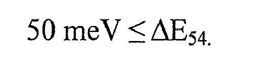
- This can prevent an electron that is to be injected from the level Lr in the
injection layer 18a of the previous period into the first light emission upper level Lup1 and the second light emission upper level Lup2 from leaking into a level higher than the light emission upper levels. Such a level structure in which the higher energy levels are separated enough from the first light emission upper level and the second light emission upper level is definitely different from the upper miniband utilizing the super lattice structure in an active layer. - An electron e- from the level Lr in the
injection layer 18a of the previous period into the quantum well light emittinglayer 17 is preferably injected into the second light emission upper level Lup2. As described above, by injecting an electron into the second light emission upper level, which is the higher level between the first light emission upper level and the second light emission upper level, carriers are distributed evenly between the two upper levels, thereby appropriately achieving light emitting transitions from the first light emission upper level and the second light emission upper level to the lower levels. - The probabilities of an electron at the first light emission upper level Lup1 and the second light emission upper level Lup2 existing in the active layer except for the first well layer of the quantum well light emitting
layer 17 are preferably 30% or more, the probabilities given by its squared wave functions. With a configuration in which the wave functions of the first light emission upper level and the second light emission upper level are not localized in the first well layer to allow an electron to exist with a sufficient probability in the second to the n-th well layers with these wave functions extending over the entirelight emitting layer 17, the first light emission upper level and the second light emission upper level each appropriately function as a level for light emitting transitions to the light emission lower levels, thereby achieving evenly light emitting transitions. - A wafer for a QCL is a layered structure of a compound semiconductor. Its mechanical strength is thus relatively low and its surface flatness is also relatively low (the maximum of about 10 µm roughness in the wafer surface). In the manufacturing method of the
QCL 1 according to the present embodiment, theresin stamper 201 made of theresin film 200 having flexibility is pressed against the resistfilm 304 by air pressure to transfer the second groove pattern P2 to the resistfilm 304. The wafer with low flatness is thus evenly pressured by the air pressure, whereby the second groove pattern P2 of theresin stamper 201 is transferred to the resistfilm 304 markedly precisely. A high-precision diffraction grating is thus obtained, which allows manufacturing of the QCL capable of stably performing single mode oscillation. - In the manufacturing method of the
QCL 1 according to the present embodiment, the mother stamper 103 with the first groove pattern P1 formed is pressed against theresin film 200 to transfer the first groove pattern P1 to theresin film 200, thereby making theresin stamper 201 with the second groove pattern P2 formed on theresin film 200, the second groove pattern P2 having the inverted asperity of the first groove pattern P1. With the mother stamper 103 made once, any number of thesame resin stampers 201 can be duplicated in a case of theresin stamper 201 being damaged. Theresin stamper 201 can be used any number of times as long as it is not damaged. - In the manufacturing method of the
QCL 1 according to the present embodiment, theresin stamper 201 is made of theresin film 200 having flexibility, and a plurality of diffraction gratings can be made at once on the wafer for theresin stamper 201 with a large area. This can improve the mass production capacity of theQCL 1. A plurality of diffraction gratings with different periods can be made at once on the wafer according to the second groove pattern P2 of theresin stamper 201. TheQCL 1 capable of performing a plurality of kinds of single mode oscillation can be made from one wafer. - In the manufacturing method of the
QCL 1 according to the present embodiment, the diffraction grating formed on the surface of the wafer is a phase shifting diffraction grating. The bimodal oscillation stemming from an error in the position of cleavage of the diffraction grating in manufacturing is thus prevented, which allows manufacturing of theQCL 1 that stably performs the single mode oscillation. A λ/4 phase shifting diffraction grating with the asperity phase of the diffraction grating inverted in the vicinity of the center of the diffraction grating is preferably adopted in the present embodiment in particular, and thus the oscillation threshold gain can be only for one mode, the minimum mode. - In the manufacturing method of the
QCL 1 according to the present embodiment, theSiN film 303 and the resistfilm 304 are sequentially stacked on the wafer (InGaAs film 302). The adhesion between the wafer (InGaAs film 302) and the resistfilm 304 is thus given by theSiN film 303, and a rip-off (a phenomenon in which part of the third pattern P3 is flaked off when theresin stamper 201 is released from the resistfilm 304 because of the adhesion between theresin stamper 201 and part of the resist film 304) can be reduced. - In the manufacturing method of the
QCL 1 according to the present embodiment, theInP film 301 and theInGaAs film 302 are formed on theintermediate structure 300 in order closest to theactive layer 15. The distance from theactive layer 15 to theInGaAs film 302 can thus be adjusted through the thickness of theInP film 301. TheInGaAs film 302 is etched to function as a diffraction grating, and thus the coupling factor of the diffraction grating can be adjusted for a wavelength by adjusting the thickness of theInP film 301 as thebase 20a. TheInP film 301 functions as a stopper during etching of theInGaAs film 302, thereby allowing a markedly precise control of the groove depth of the diffraction grating. - In the manufacturing method of the
QCL 1 according to the present embodiment, the resistfilm 304 is formed of ultraviolet curable resin, and theresin stamper 201 has ultraviolet transparency. While theresin stamper 201 is press-bonded to the resistfilm 304, ultraviolet light can thus be applied through theresin stamper 201 to the resistfilm 304. - The QCL according to the present invention is not limited to the embodiment and the configuration example described above but allows various modifications. The configuration example above describes an example with the semiconductor substrate using the InP substrate and the active layer made of InGaAs/InAlAs, but various configurations can be adopted as long as they allow light emitting transition through intersubband transition in a quantum well structure and realization of the subband level structure described above.
- As such a semiconductor material, various materials other than InGaAs/InAlAs described above can be used such as GaAs/AlGaAs, InAs/AlSb, GaN/AlGaN, and SiGe/Si. Various methods may be used as a semiconductor crystal growth method.
- Various structures other than those illustrated in
Figs. 1 ,3 , and4 , may be adopted as the layered structure in the active layer of the QCL and the semiconductor layered structure as the entire laser device. The QCL typically needs to include the semiconductor substrate and the active layer disposed on the semiconductor substrate and having the configuration described above. The above configuration example describes the configuration lattice-matched to the InP substrate, but a configuration lattice-mismatched to the InP substrate may be adopted. This configuration can increase flexibility in device design, and achieve effective carrier confinement and shortened oscillation wavelength. - In the present embodiment, the
diffraction grating layer 20 is formed as a λ/4 phase shifting diffraction grating, but may be a diffraction grating with a phase shifting amount other than λ/4. The λ/4 phase shifting diffraction grating, however, is preferably adopted as in the present embodiment because the oscillation threshold gain is then only for one mode, the minimum mode. - In the present embodiment, the
diffraction grating layer 20 includes thebase 20a, but the protrusions 20b may be directly disposed on the active layer 15 (the upper core layer 12) without thebase 20a. That is, theInGaAs layer 302, theSiN film 303, and the resistfilm 304 are sequentially stacked on a surface of theintermediate structure 300 to form the diffraction grating. - In the present embodiment, the
SiN film 303 is formed as an intermediate layer between the wafer and the resistfilm 304, but a SiO2 film may be formed in place of theSiN film 303 or such an intermediate layer may need not to be provided. - In the present embodiment, the
InP substrate 100 is used as themother stamper 103, but other materials or other processing methods may be selected as long as precise processing is possible. -
- 1 ... QCL, 10 ... semiconductor substrate, 11 ... lower core layer, 12 ... upper core layer, 13 ... cladding layer, 14 ... contact layer, 15 ... active layer, 16 ... unit layered structure, 17 ... quantum well light emitting layer, 18 ... injection layer, 20 ... diffraction grating, 303 ... SiN film (intermediate film), P1 ... first groove pattern, P2 ... second groove pattern, P3 ... third groove pattern.
Claims (6)
- A quantum cascade laser manufacturing method comprising:a first step of preparing a mother stamper with a predetermined first groove pattern formed on a surface of a substrate;a second step of pressing the mother stamper against a resin film having flexibility to transfer the first groove pattern to the resin film and making a resin stamper with a second groove pattern formed on the resin film, the second groove pattern having an inverted asperity of the first groove pattern;a third step of making a wafer with an active layer formed on a semiconductor substrate, the active layer having a cascade structure in which a unit layered structure including a quantum well light emitting layer and an injection layer is stacked in multiples to alternately stack the quantum well light emitting layer and the injection layer;a fourth step of forming a resist film on a surface on the active layer side of the wafer;a fifth step of pressing the resin stamper against the resist film by air pressure to transfer the second groove pattern to the resist film and forming on the resist film a third groove pattern having an inverted asperity of the second groove pattern; anda sixth step of etching the wafer with the resist film serving as a mask to form a diffraction grating on a surface of the wafer.
- The method according to claim 1, wherein the diffraction grating formed on the surface of the wafer in the sixth step is a phase shifting diffraction grating.
- The method according to claim 1 or 2, further comprising:a step of forming an intermediate film on the surface on the active layer side of the wafer, after the third step and before the fourth step.
- The method according to claim 3, wherein the intermediate film is a SiN film or a SiO2 film.
- The method according to any one of claims 1 to 4, wherein an InP film and an InGaAs film are formed on the active layer side of the wafer in order closest to the active layer.
- The method according to any one of claims 1 to 5, wherein the resist film is formed of ultraviolet curable resin and the resin stamper has ultraviolet transparency.
Applications Claiming Priority (2)
| Application Number | Priority Date | Filing Date | Title |
|---|---|---|---|
| JP2011237704A JP5771120B2 (en) | 2011-10-28 | 2011-10-28 | Manufacturing method of quantum cascade laser |
| PCT/JP2012/067116 WO2013061656A1 (en) | 2011-10-28 | 2012-07-04 | Quantum cascade laser manufacturing method |
Publications (3)
| Publication Number | Publication Date |
|---|---|
| EP2787583A1 true EP2787583A1 (en) | 2014-10-08 |
| EP2787583A4 EP2787583A4 (en) | 2015-07-01 |
| EP2787583B1 EP2787583B1 (en) | 2018-11-14 |
Family
ID=48167500
Family Applications (1)
| Application Number | Title | Priority Date | Filing Date |
|---|---|---|---|
| EP12843865.2A Active EP2787583B1 (en) | 2011-10-28 | 2012-07-04 | Quantum cascade laser manufacturing method |
Country Status (4)
| Country | Link |
|---|---|
| US (1) | US9620921B2 (en) |
| EP (1) | EP2787583B1 (en) |
| JP (1) | JP5771120B2 (en) |
| WO (1) | WO2013061656A1 (en) |
Families Citing this family (5)
| Publication number | Priority date | Publication date | Assignee | Title |
|---|---|---|---|---|
| JP6276758B2 (en) * | 2013-05-23 | 2018-02-07 | 浜松ホトニクス株式会社 | Quantum cascade laser |
| JP6467193B2 (en) * | 2014-10-30 | 2019-02-06 | 浜松ホトニクス株式会社 | Quantum cascade laser |
| FR3040246B1 (en) * | 2015-08-20 | 2017-09-29 | Centre Nat Rech Scient | LASER TERAHERTZ, TERAHERTZ SOURCE AND USE OF SUCH LASER TERAHERTZ |
| JP7203282B1 (en) * | 2022-01-24 | 2023-01-12 | 三菱電機株式会社 | Quantum cascade laser device manufacturing method and quantum cascade laser device |
| US20250341677A1 (en) * | 2023-01-17 | 2025-11-06 | Applied Materials, Inc. | Low frequency imprint for grayscale optical device fabrication |
Family Cites Families (29)
| Publication number | Priority date | Publication date | Assignee | Title |
|---|---|---|---|---|
| US5509025A (en) | 1994-04-04 | 1996-04-16 | At&T Corp. | Unipolar semiconductor laser |
| US5457709A (en) | 1994-04-04 | 1995-10-10 | At&T Ipm Corp. | Unipolar semiconductor laser |
| US5727010A (en) | 1996-03-20 | 1998-03-10 | Lucent Technologies Inc. | Article comprising an improved quantum cascade laser |
| JPH09312437A (en) * | 1996-05-24 | 1997-12-02 | Matsushita Electric Ind Co Ltd | Semiconductor laser and manufacturing method thereof |
| US5745516A (en) | 1996-11-06 | 1998-04-28 | Lucent Technologies Inc. | Article comprising a unipolar superlattice laser |
| JP3332851B2 (en) * | 1998-04-22 | 2002-10-07 | 松下電器産業株式会社 | Method for manufacturing semiconductor device |
| US6560259B1 (en) * | 2000-05-31 | 2003-05-06 | Applied Optoelectronics, Inc. | Spatially coherent surface-emitting, grating coupled quantum cascade laser with unstable resonance cavity |
| EP1195865A1 (en) | 2000-08-31 | 2002-04-10 | Alpes Lasers SA | Quantum cascade laser |
| EP1189317A1 (en) | 2000-09-13 | 2002-03-20 | Alpes Lasers SA | Quantum cascade Laser with optical phonon excitation |
| US20040121545A1 (en) * | 2002-12-23 | 2004-06-24 | Taiwan Semiconductor Manufacturing Company | Method to fabricate a square word line poly spacer |
| US6638773B1 (en) * | 2002-05-31 | 2003-10-28 | Applied Optoelectronics, Inc. | Method for fabricating single-mode DBR laser with improved yield |
| US7036209B1 (en) * | 2002-07-01 | 2006-05-02 | Seagate Technology Llc | Method of simultaneously forming magnetic transition patterns of a dual side recording medium |
| JP4735280B2 (en) * | 2006-01-18 | 2011-07-27 | 株式会社日立製作所 | Pattern formation method |
| JP4641321B2 (en) * | 2006-03-27 | 2011-03-02 | パイオニア株式会社 | Mold for pattern transfer |
| JP2008060396A (en) | 2006-08-31 | 2008-03-13 | Hamamatsu Photonics Kk | Quantum cascade laser |
| JP5641667B2 (en) | 2007-01-18 | 2014-12-17 | 浜松ホトニクス株式会社 | Quantum cascade laser |
| JP5372349B2 (en) * | 2007-08-23 | 2013-12-18 | 浜松ホトニクス株式会社 | Quantum cascade laser device |
| JP5205866B2 (en) * | 2007-08-23 | 2013-06-05 | 住友電気工業株式会社 | Mold forming method, diffraction grating forming method, and distributed feedback semiconductor laser manufacturing method |
| WO2009078881A1 (en) * | 2007-12-19 | 2009-06-25 | Hewlett-Packard Development Company, L.P. | Imprint lithography apparatus and method |
| JP5092740B2 (en) * | 2007-12-28 | 2012-12-05 | 住友電気工業株式会社 | Manufacturing method of semiconductor device |
| JP4815464B2 (en) * | 2008-03-31 | 2011-11-16 | 株式会社日立製作所 | Fine structure transfer stamper and fine structure transfer apparatus |
| JP5117318B2 (en) * | 2008-08-07 | 2013-01-16 | 株式会社日立ハイテクノロジーズ | Nanoimprinting stamper and fine structure transfer apparatus using the stamper |
| WO2010044756A2 (en) * | 2008-10-16 | 2010-04-22 | Teng Hwee Koh | Mold imprinting |
| JP5326806B2 (en) * | 2009-05-21 | 2013-10-30 | 住友電気工業株式会社 | Method for fabricating a semiconductor optical device |
| JP5232077B2 (en) * | 2009-06-02 | 2013-07-10 | 株式会社日立ハイテクノロジーズ | Microstructure transfer device |
| JP2011023660A (en) * | 2009-07-17 | 2011-02-03 | Toshiba Corp | Pattern transfer method |
| JP4768848B2 (en) * | 2009-12-07 | 2011-09-07 | 株式会社東芝 | Electroforming master and its manufacturing method |
| JP2011134870A (en) * | 2009-12-24 | 2011-07-07 | Sumitomo Electric Ind Ltd | Ridge semiconductor laser and method of manufacturing the same |
| US20110195276A1 (en) * | 2010-02-11 | 2011-08-11 | Seagate Technology Llc | Resist adhension to carbon overcoats for nanoimprint lithography |
-
2011
- 2011-10-28 JP JP2011237704A patent/JP5771120B2/en active Active
-
2012
- 2012-07-04 US US14/342,895 patent/US9620921B2/en active Active
- 2012-07-04 EP EP12843865.2A patent/EP2787583B1/en active Active
- 2012-07-04 WO PCT/JP2012/067116 patent/WO2013061656A1/en not_active Ceased
Also Published As
| Publication number | Publication date |
|---|---|
| EP2787583A4 (en) | 2015-07-01 |
| EP2787583B1 (en) | 2018-11-14 |
| US9620921B2 (en) | 2017-04-11 |
| WO2013061656A1 (en) | 2013-05-02 |
| US20140199798A1 (en) | 2014-07-17 |
| JP5771120B2 (en) | 2015-08-26 |
| JP2013098252A (en) | 2013-05-20 |
Similar Documents
| Publication | Publication Date | Title |
|---|---|---|
| US8958450B2 (en) | Quantum cascade laser | |
| JP5523759B2 (en) | Quantum cascade laser | |
| US9547124B2 (en) | Waveguide structure for mid-IR multiwavelength concatenated distributed-feedback laser with an active core made of cascaded stages | |
| Coleman et al. | Semiconductor quantum dot lasers: a tutorial | |
| US20080310470A1 (en) | Broadband semiconductor laser | |
| Baranov et al. | Quantum cascade lasers in the InAs/AlSb material system | |
| EP2787583B1 (en) | Quantum cascade laser manufacturing method | |
| CA2348005C (en) | Flat minibands with spatially symmetric wavefunctions in intersubband superlattice light emitters | |
| US8514903B2 (en) | Quantum cascade laser | |
| EP2803122B1 (en) | Mid-ir multiwavelength concatenated distributed-feedback laser with an active core made of cascaded stages | |
| JP2015536576A (en) | Multiwavelength quantum cascade lasers with different active and inert core growth | |
| WO2017123309A2 (en) | Monolithical widely tunable quantum cascade laser devices | |
| US9484715B2 (en) | Quantum-cascade laser | |
| US10630058B2 (en) | Quantum cascade laser | |
| Bradshaw et al. | Single-longitudinal-mode emission from interband cascade DFB laser with a grating fabricated by interferometric lithography | |
| US9276380B2 (en) | Spontaneous and stimulated emission control using quantum-structure lattice arrays | |
| Yoshinaga et al. | Low power consumption (< 1 W) mid-infrared quantum cascade laser for gas sensing | |
| Mamutin et al. | MBE growth and characterization of 5-μm quantum-cascade lasers | |
| Baranov et al. | 3 Long-Wavelength Mid-Infrared Quantum Cascade Lasers | |
| Chang | Step-tapered active-region mid-infrared quantum cascade lasers and novel fabrication processes for buried heterostructures | |
| Razeghi | New frontiers in InP based quantum devices | |
| Viheriala et al. | Surface-grating-based distributed feedback lasers fabricated using nanoimprint lithography |
Legal Events
| Date | Code | Title | Description |
|---|---|---|---|
| PUAI | Public reference made under article 153(3) epc to a published international application that has entered the european phase |
Free format text: ORIGINAL CODE: 0009012 |
|
| 17P | Request for examination filed |
Effective date: 20140128 |
|
| AK | Designated contracting states |
Kind code of ref document: A1 Designated state(s): AL AT BE BG CH CY CZ DE DK EE ES FI FR GB GR HR HU IE IS IT LI LT LU LV MC MK MT NL NO PL PT RO RS SE SI SK SM TR |
|
| DAX | Request for extension of the european patent (deleted) | ||
| RA4 | Supplementary search report drawn up and despatched (corrected) |
Effective date: 20150601 |
|
| RIC1 | Information provided on ipc code assigned before grant |
Ipc: B29C 33/40 20060101ALI20150526BHEP Ipc: H01S 5/0687 20060101ALI20150526BHEP Ipc: H01L 21/027 20060101ALI20150526BHEP Ipc: B29C 59/02 20060101ALI20150526BHEP Ipc: H01S 5/12 20060101AFI20150526BHEP |
|
| GRAP | Despatch of communication of intention to grant a patent |
Free format text: ORIGINAL CODE: EPIDOSNIGR1 |
|
| STAA | Information on the status of an ep patent application or granted ep patent |
Free format text: STATUS: GRANT OF PATENT IS INTENDED |
|
| INTG | Intention to grant announced |
Effective date: 20180619 |
|
| GRAJ | Information related to disapproval of communication of intention to grant by the applicant or resumption of examination proceedings by the epo deleted |
Free format text: ORIGINAL CODE: EPIDOSDIGR1 |
|
| STAA | Information on the status of an ep patent application or granted ep patent |
Free format text: STATUS: REQUEST FOR EXAMINATION WAS MADE |
|
| GRAR | Information related to intention to grant a patent recorded |
Free format text: ORIGINAL CODE: EPIDOSNIGR71 |
|
| GRAS | Grant fee paid |
Free format text: ORIGINAL CODE: EPIDOSNIGR3 |
|
| STAA | Information on the status of an ep patent application or granted ep patent |
Free format text: STATUS: GRANT OF PATENT IS INTENDED |
|
| GRAA | (expected) grant |
Free format text: ORIGINAL CODE: 0009210 |
|
| STAA | Information on the status of an ep patent application or granted ep patent |
Free format text: STATUS: THE PATENT HAS BEEN GRANTED |
|
| INTC | Intention to grant announced (deleted) | ||
| AK | Designated contracting states |
Kind code of ref document: B1 Designated state(s): AL AT BE BG CH CY CZ DE DK EE ES FI FR GB GR HR HU IE IS IT LI LT LU LV MC MK MT NL NO PL PT RO RS SE SI SK SM TR |
|
| INTG | Intention to grant announced |
Effective date: 20181008 |
|
| REG | Reference to a national code |
Ref country code: CH Ref legal event code: EP Ref country code: AT Ref legal event code: REF Ref document number: 1065955 Country of ref document: AT Kind code of ref document: T Effective date: 20181115 |
|
| REG | Reference to a national code |
Ref country code: DE Ref legal event code: R096 Ref document number: 602012053605 Country of ref document: DE |
|
| REG | Reference to a national code |
Ref country code: IE Ref legal event code: FG4D |
|
| REG | Reference to a national code |
Ref country code: NL Ref legal event code: MP Effective date: 20181114 |
|
| REG | Reference to a national code |
Ref country code: LT Ref legal event code: MG4D |
|
| REG | Reference to a national code |
Ref country code: AT Ref legal event code: MK05 Ref document number: 1065955 Country of ref document: AT Kind code of ref document: T Effective date: 20181114 |
|
| PG25 | Lapsed in a contracting state [announced via postgrant information from national office to epo] |
Ref country code: LT Free format text: LAPSE BECAUSE OF FAILURE TO SUBMIT A TRANSLATION OF THE DESCRIPTION OR TO PAY THE FEE WITHIN THE PRESCRIBED TIME-LIMIT Effective date: 20181114 Ref country code: HR Free format text: LAPSE BECAUSE OF FAILURE TO SUBMIT A TRANSLATION OF THE DESCRIPTION OR TO PAY THE FEE WITHIN THE PRESCRIBED TIME-LIMIT Effective date: 20181114 Ref country code: AT Free format text: LAPSE BECAUSE OF FAILURE TO SUBMIT A TRANSLATION OF THE DESCRIPTION OR TO PAY THE FEE WITHIN THE PRESCRIBED TIME-LIMIT Effective date: 20181114 Ref country code: BG Free format text: LAPSE BECAUSE OF FAILURE TO SUBMIT A TRANSLATION OF THE DESCRIPTION OR TO PAY THE FEE WITHIN THE PRESCRIBED TIME-LIMIT Effective date: 20190214 Ref country code: IS Free format text: LAPSE BECAUSE OF FAILURE TO SUBMIT A TRANSLATION OF THE DESCRIPTION OR TO PAY THE FEE WITHIN THE PRESCRIBED TIME-LIMIT Effective date: 20190314 Ref country code: ES Free format text: LAPSE BECAUSE OF FAILURE TO SUBMIT A TRANSLATION OF THE DESCRIPTION OR TO PAY THE FEE WITHIN THE PRESCRIBED TIME-LIMIT Effective date: 20181114 Ref country code: NO Free format text: LAPSE BECAUSE OF FAILURE TO SUBMIT A TRANSLATION OF THE DESCRIPTION OR TO PAY THE FEE WITHIN THE PRESCRIBED TIME-LIMIT Effective date: 20190214 Ref country code: FI Free format text: LAPSE BECAUSE OF FAILURE TO SUBMIT A TRANSLATION OF THE DESCRIPTION OR TO PAY THE FEE WITHIN THE PRESCRIBED TIME-LIMIT Effective date: 20181114 Ref country code: LV Free format text: LAPSE BECAUSE OF FAILURE TO SUBMIT A TRANSLATION OF THE DESCRIPTION OR TO PAY THE FEE WITHIN THE PRESCRIBED TIME-LIMIT Effective date: 20181114 |
|
| PG25 | Lapsed in a contracting state [announced via postgrant information from national office to epo] |
Ref country code: SE Free format text: LAPSE BECAUSE OF FAILURE TO SUBMIT A TRANSLATION OF THE DESCRIPTION OR TO PAY THE FEE WITHIN THE PRESCRIBED TIME-LIMIT Effective date: 20181114 Ref country code: AL Free format text: LAPSE BECAUSE OF FAILURE TO SUBMIT A TRANSLATION OF THE DESCRIPTION OR TO PAY THE FEE WITHIN THE PRESCRIBED TIME-LIMIT Effective date: 20181114 Ref country code: RS Free format text: LAPSE BECAUSE OF FAILURE TO SUBMIT A TRANSLATION OF THE DESCRIPTION OR TO PAY THE FEE WITHIN THE PRESCRIBED TIME-LIMIT Effective date: 20181114 Ref country code: GR Free format text: LAPSE BECAUSE OF FAILURE TO SUBMIT A TRANSLATION OF THE DESCRIPTION OR TO PAY THE FEE WITHIN THE PRESCRIBED TIME-LIMIT Effective date: 20190215 Ref country code: NL Free format text: LAPSE BECAUSE OF FAILURE TO SUBMIT A TRANSLATION OF THE DESCRIPTION OR TO PAY THE FEE WITHIN THE PRESCRIBED TIME-LIMIT Effective date: 20181114 Ref country code: PT Free format text: LAPSE BECAUSE OF FAILURE TO SUBMIT A TRANSLATION OF THE DESCRIPTION OR TO PAY THE FEE WITHIN THE PRESCRIBED TIME-LIMIT Effective date: 20190314 |
|
| PG25 | Lapsed in a contracting state [announced via postgrant information from national office to epo] |
Ref country code: PL Free format text: LAPSE BECAUSE OF FAILURE TO SUBMIT A TRANSLATION OF THE DESCRIPTION OR TO PAY THE FEE WITHIN THE PRESCRIBED TIME-LIMIT Effective date: 20181114 Ref country code: DK Free format text: LAPSE BECAUSE OF FAILURE TO SUBMIT A TRANSLATION OF THE DESCRIPTION OR TO PAY THE FEE WITHIN THE PRESCRIBED TIME-LIMIT Effective date: 20181114 Ref country code: IT Free format text: LAPSE BECAUSE OF FAILURE TO SUBMIT A TRANSLATION OF THE DESCRIPTION OR TO PAY THE FEE WITHIN THE PRESCRIBED TIME-LIMIT Effective date: 20181114 Ref country code: CZ Free format text: LAPSE BECAUSE OF FAILURE TO SUBMIT A TRANSLATION OF THE DESCRIPTION OR TO PAY THE FEE WITHIN THE PRESCRIBED TIME-LIMIT Effective date: 20181114 |
|
| REG | Reference to a national code |
Ref country code: DE Ref legal event code: R097 Ref document number: 602012053605 Country of ref document: DE |
|
| PG25 | Lapsed in a contracting state [announced via postgrant information from national office to epo] |
Ref country code: RO Free format text: LAPSE BECAUSE OF FAILURE TO SUBMIT A TRANSLATION OF THE DESCRIPTION OR TO PAY THE FEE WITHIN THE PRESCRIBED TIME-LIMIT Effective date: 20181114 Ref country code: EE Free format text: LAPSE BECAUSE OF FAILURE TO SUBMIT A TRANSLATION OF THE DESCRIPTION OR TO PAY THE FEE WITHIN THE PRESCRIBED TIME-LIMIT Effective date: 20181114 Ref country code: SM Free format text: LAPSE BECAUSE OF FAILURE TO SUBMIT A TRANSLATION OF THE DESCRIPTION OR TO PAY THE FEE WITHIN THE PRESCRIBED TIME-LIMIT Effective date: 20181114 Ref country code: SK Free format text: LAPSE BECAUSE OF FAILURE TO SUBMIT A TRANSLATION OF THE DESCRIPTION OR TO PAY THE FEE WITHIN THE PRESCRIBED TIME-LIMIT Effective date: 20181114 |
|
| PLBE | No opposition filed within time limit |
Free format text: ORIGINAL CODE: 0009261 |
|
| STAA | Information on the status of an ep patent application or granted ep patent |
Free format text: STATUS: NO OPPOSITION FILED WITHIN TIME LIMIT |
|
| 26N | No opposition filed |
Effective date: 20190815 |
|
| PG25 | Lapsed in a contracting state [announced via postgrant information from national office to epo] |
Ref country code: SI Free format text: LAPSE BECAUSE OF FAILURE TO SUBMIT A TRANSLATION OF THE DESCRIPTION OR TO PAY THE FEE WITHIN THE PRESCRIBED TIME-LIMIT Effective date: 20181114 |
|
| PG25 | Lapsed in a contracting state [announced via postgrant information from national office to epo] |
Ref country code: MC Free format text: LAPSE BECAUSE OF FAILURE TO SUBMIT A TRANSLATION OF THE DESCRIPTION OR TO PAY THE FEE WITHIN THE PRESCRIBED TIME-LIMIT Effective date: 20181114 |
|
| REG | Reference to a national code |
Ref country code: CH Ref legal event code: PL |
|
| PG25 | Lapsed in a contracting state [announced via postgrant information from national office to epo] |
Ref country code: TR Free format text: LAPSE BECAUSE OF FAILURE TO SUBMIT A TRANSLATION OF THE DESCRIPTION OR TO PAY THE FEE WITHIN THE PRESCRIBED TIME-LIMIT Effective date: 20181114 |
|
| REG | Reference to a national code |
Ref country code: BE Ref legal event code: MM Effective date: 20190731 |
|
| PG25 | Lapsed in a contracting state [announced via postgrant information from national office to epo] |
Ref country code: BE Free format text: LAPSE BECAUSE OF NON-PAYMENT OF DUE FEES Effective date: 20190731 Ref country code: LU Free format text: LAPSE BECAUSE OF NON-PAYMENT OF DUE FEES Effective date: 20190704 Ref country code: LI Free format text: LAPSE BECAUSE OF NON-PAYMENT OF DUE FEES Effective date: 20190731 Ref country code: CH Free format text: LAPSE BECAUSE OF NON-PAYMENT OF DUE FEES Effective date: 20190731 |
|
| PG25 | Lapsed in a contracting state [announced via postgrant information from national office to epo] |
Ref country code: IE Free format text: LAPSE BECAUSE OF NON-PAYMENT OF DUE FEES Effective date: 20190704 |
|
| PG25 | Lapsed in a contracting state [announced via postgrant information from national office to epo] |
Ref country code: CY Free format text: LAPSE BECAUSE OF FAILURE TO SUBMIT A TRANSLATION OF THE DESCRIPTION OR TO PAY THE FEE WITHIN THE PRESCRIBED TIME-LIMIT Effective date: 20181114 |
|
| PG25 | Lapsed in a contracting state [announced via postgrant information from national office to epo] |
Ref country code: HU Free format text: LAPSE BECAUSE OF FAILURE TO SUBMIT A TRANSLATION OF THE DESCRIPTION OR TO PAY THE FEE WITHIN THE PRESCRIBED TIME-LIMIT; INVALID AB INITIO Effective date: 20120704 Ref country code: MT Free format text: LAPSE BECAUSE OF FAILURE TO SUBMIT A TRANSLATION OF THE DESCRIPTION OR TO PAY THE FEE WITHIN THE PRESCRIBED TIME-LIMIT Effective date: 20181114 |
|
| PG25 | Lapsed in a contracting state [announced via postgrant information from national office to epo] |
Ref country code: MK Free format text: LAPSE BECAUSE OF FAILURE TO SUBMIT A TRANSLATION OF THE DESCRIPTION OR TO PAY THE FEE WITHIN THE PRESCRIBED TIME-LIMIT Effective date: 20181114 |
|
| P01 | Opt-out of the competence of the unified patent court (upc) registered |
Effective date: 20230509 |
|
| PGFP | Annual fee paid to national office [announced via postgrant information from national office to epo] |
Ref country code: GB Payment date: 20250529 Year of fee payment: 14 |
|
| PGFP | Annual fee paid to national office [announced via postgrant information from national office to epo] |
Ref country code: FR Payment date: 20250610 Year of fee payment: 14 |
|
| PGFP | Annual fee paid to national office [announced via postgrant information from national office to epo] |
Ref country code: DE Payment date: 20250528 Year of fee payment: 14 |