EP2787575A1 - Antenna apparatus and communication apparatus - Google Patents
Antenna apparatus and communication apparatus Download PDFInfo
- Publication number
- EP2787575A1 EP2787575A1 EP12854142.2A EP12854142A EP2787575A1 EP 2787575 A1 EP2787575 A1 EP 2787575A1 EP 12854142 A EP12854142 A EP 12854142A EP 2787575 A1 EP2787575 A1 EP 2787575A1
- Authority
- EP
- European Patent Office
- Prior art keywords
- antenna
- antenna coil
- magnetic sheet
- transmitter
- coil
- Prior art date
- Legal status (The legal status is an assumption and is not a legal conclusion. Google has not performed a legal analysis and makes no representation as to the accuracy of the status listed.)
- Granted
Links
Images



Classifications
-
- H—ELECTRICITY
- H01—ELECTRIC ELEMENTS
- H01Q—ANTENNAS, i.e. RADIO AERIALS
- H01Q1/00—Details of, or arrangements associated with, antennas
- H01Q1/36—Structural form of radiating elements, e.g. cone, spiral, umbrella; Particular materials used therewith
- H01Q1/38—Structural form of radiating elements, e.g. cone, spiral, umbrella; Particular materials used therewith formed by a conductive layer on an insulating support
-
- H—ELECTRICITY
- H01—ELECTRIC ELEMENTS
- H01Q—ANTENNAS, i.e. RADIO AERIALS
- H01Q1/00—Details of, or arrangements associated with, antennas
- H01Q1/12—Supports; Mounting means
- H01Q1/22—Supports; Mounting means by structural association with other equipment or articles
- H01Q1/24—Supports; Mounting means by structural association with other equipment or articles with receiving set
-
- G—PHYSICS
- G06—COMPUTING OR CALCULATING; COUNTING
- G06K—GRAPHICAL DATA READING; PRESENTATION OF DATA; RECORD CARRIERS; HANDLING RECORD CARRIERS
- G06K19/00—Record carriers for use with machines and with at least a part designed to carry digital markings
- G06K19/06—Record carriers for use with machines and with at least a part designed to carry digital markings characterised by the kind of the digital marking, e.g. shape, nature, code
- G06K19/067—Record carriers with conductive marks, printed circuits or semiconductor circuit elements, e.g. credit or identity cards also with resonating or responding marks without active components
- G06K19/07—Record carriers with conductive marks, printed circuits or semiconductor circuit elements, e.g. credit or identity cards also with resonating or responding marks without active components with integrated circuit chips
- G06K19/077—Constructional details, e.g. mounting of circuits in the carrier
- G06K19/07749—Constructional details, e.g. mounting of circuits in the carrier the record carrier being capable of non-contact communication, e.g. constructional details of the antenna of a non-contact smart card
- G06K19/07771—Constructional details, e.g. mounting of circuits in the carrier the record carrier being capable of non-contact communication, e.g. constructional details of the antenna of a non-contact smart card the record carrier comprising means for minimising adverse effects on the data communication capability of the record carrier, e.g. minimising Eddy currents induced in a proximate metal or otherwise electromagnetically interfering object
-
- H—ELECTRICITY
- H01—ELECTRIC ELEMENTS
- H01Q—ANTENNAS, i.e. RADIO AERIALS
- H01Q1/00—Details of, or arrangements associated with, antennas
- H01Q1/12—Supports; Mounting means
- H01Q1/22—Supports; Mounting means by structural association with other equipment or articles
- H01Q1/2208—Supports; Mounting means by structural association with other equipment or articles associated with components used in interrogation type services, i.e. in systems for information exchange between an interrogator/reader and a tag/transponder, e.g. in Radio Frequency Identification [RFID] systems
- H01Q1/2225—Supports; Mounting means by structural association with other equipment or articles associated with components used in interrogation type services, i.e. in systems for information exchange between an interrogator/reader and a tag/transponder, e.g. in Radio Frequency Identification [RFID] systems used in active tags, i.e. provided with its own power source or in passive tags, i.e. deriving power from RF signal
-
- H—ELECTRICITY
- H01—ELECTRIC ELEMENTS
- H01Q—ANTENNAS, i.e. RADIO AERIALS
- H01Q7/00—Loop antennas with a substantially uniform current distribution around the loop and having a directional radiation pattern in a plane perpendicular to the plane of the loop
- H01Q7/06—Loop antennas with a substantially uniform current distribution around the loop and having a directional radiation pattern in a plane perpendicular to the plane of the loop with core of ferromagnetic material
Definitions
- the present invention relates to an antenna apparatus that is assembled into an electronic apparatus and can be communicated upon receipt of a magnetic field transmitted from a transmitter, and a communication apparatus.
- an antenna module for an RFID (Radio Frequency Identification) has been used for installing a function for near non-contact communication therein.
- This antenna module carries out a communication by utilizing an inductive coupling with an antenna coil mounted on a transmitter such as a reader writer. That is, by allowing its antenna coil to receive a magnetic field from the reader writer, this antenna module converts it into electric power and makes it possible to drive an IC that functions as a communication processing unit.
- an antenna module In order to positively carry out communication, the antenna module needs to receive a magnetic flux of a predetermined value or more by the antenna coil from the reader writer. For this reason, an antenna module according to a conventional example installs a loop coil in a casing of the portable telephone, and receives the magnetic flux from the reader writer by using this coil.
- the antenna module assembled into an electronic apparatus such as a portable telephone, since the magnetic flux from the reader writer is repelled by an eddy current that is generated by metals for use in substrates, battery packs or the like inside the apparatus, when they receive a magnetic field from the reader writer, the magnetic flux reaching the loop coil becomes smaller. Since the magnetic flux reaching the loop coil becomes smaller in this manner, the antenna module requires a loop coil having a certain size for collecting required magnetic fluxes, and it is further necessary to use a magnetic sheet so as to increase the magnetic fluxes.
- Patent Document 1 has proposed an apparatus in which, by receiving this component, a function for an antenna is exerted. More specifically, Patent Document 1 has proposed an antenna structure in which a coil is wound around a ferrite core so as to reduce the occupied area of the coil.
- a magnetic field is repelled by an eddy current generated in the substrate that has received the magnetic field.
- the magnetic field that is applied from the reader writer tends to become stronger on the outer peripheral portion of the casing surface, while it tends to become weaker in the vicinity of the center of the casing surface.
- the opening portion of the loop coil is positioned in the center portion of the portable telephone that is not allowed to receive the magnetic field passing through the above-mentioned outer peripheral portion of the casing surface so much. For this reason, in the case of an antenna using the normal loop coil, its efficiency for receiving a magnetic field becomes poor.
- the present invention has been proposed in view of these circumstances, and its object is to provide a communication apparatus which, while maintaining a communication characteristic, makes it possible to downsize a casing of an electronic apparatus when assembled into the electronic apparatus.
- the present invention relates to an antenna apparatus that is assembled into an electronic apparatus and can be communicated upon receipt of a magnetic field transmitted from a transmitter, and the antenna apparatus is provided with an antenna substrate on which an antenna coil that is inductively coupled to the transmitter is formed, and a magnetic sheet that draws a magnetic field transmitted from the transmitter into the antenna coil, and this structure is characterized in that since the magnetic sheet is inserted into the center portion of the antenna coil formed on the antenna substrate, the two ends of the magnetic sheet are located at positions closer to the center portion in the inserting direction than the two ends of the antenna coil in the inserting direction.
- the present invention relates to a communication apparatus that can be communicated upon receipt of a magnetic field transmitted from a transmitter
- the communication apparatus is characterized by having an antenna substrate on which an antenna coil that is inductively coupled to the transmitter is formed, a magnetic sheet that draws a magnetic field transmitted from the transmitter into the antenna coil, and a communication processing unit that is driven by an electric current flowing through the antenna coil, and carries out communication between the transmitter, and since the magnetic sheet is inserted into the center portion of the antenna coil formed on the antenna substrate, the antenna coil and the magnetic sheet are mutually superimposed in a manner so as to satisfy both of an arrangement condition in which the magnetic sheet is positioned closer to the transmitter than the antenna coil on the upstream side in the proceeding direction of the magnetic field oriented by the casing surface that is opposed to the transmitter and an arrangement condition in which the antenna coil is positioned closer to the transmitter side than the magnetic sheet on the downstream side in the oriented proceeding direction, and the magnetic sheet is characterized in that in the inserting direction into the center portion of the antenna coil, two ends of the
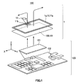
- the communication apparatus to which the present invention is applied is an apparatus that is assembled into an electronic apparatus and can be communicated upon receipt of a magnetic field transmitted from a transmitter, and is incorporated into a radio communication system 100 for an RFID (Radio Frequency Identification), for example, as shown in Fig. 1 , and used.
- RFID Radio Frequency Identification
- the radio communication system 100 is composed of a communication apparatus 1 to which the present invention is applied and a reader writer 120 that accesses the communication apparatus 1.
- the communication apparatus 1 and the reader writer 120 are supposed to be disposed so as to be made face to face with each other on the xy plane of a three-dimensional orthogonal coordinate system xyz.
- the reader writer 120 functions as a transmitter for transmitting a magnetic field in the z-axis direction to the communication apparatus 1 that is made face to face with each other thereto on the xy plane, and is more specifically provided with an antenna 121 that transmits a magnetic field toward the communication apparatus 1 and a control substrate 122 that communicates with the communication apparatus 1 that is inductively coupled thereto through the antenna 121.
- the reader writer 120 is provided with the control substrate 122 that is electrically connected to the antenna 121.
- a control circuit which is made of electronic parts, such as one or a plurality of electronic integrated circuit chips, is assembled.
- the control circuit executes various processes based upon data received from the communication apparatus 1. For example, when transmitting data to the communication apparatus 1, the control circuit encodes data, and based upon the encoded data, modulates a carrier wave having a predetermined frequency (for example, 13.56 MHz), amplifies a modulation signal thus modulated, and drives the antenna 121 by using the amplified modulation signal.
- a predetermined frequency for example, 13.56 MHz
- the control circuit when reading out data from the communication apparatus 1, the control circuit amplifies the modulation signal of data received by the antenna 121, demodulates the modulation signal of the amplified data, and decodes the data thus demodulated. Additionally, in the control circuit, an encoding system and a modulation system generally used in a reader writer are adopted, and, for example, a Manchester encoding system and an ASK (Amplitude Shift Keying) modulation system are used.
- a Manchester encoding system and an ASK (Amplitude Shift Keying) modulation system are used.
- the communication apparatus 1 is provided with an antenna module 1 a having an antenna substrate 11 in which an antenna coil 11 a, which is assembled into a casing 131 of a portable telephone 130 disposed so as to be made face to face with, for example, the reader writer 120 on the xy plane, and can be communicated with the reader writer 120 inductively coupled thereto, is assembled, and a communication processing unit 12 that is driven by an electric current flowing through the antenna coil 11a, and communicates with the reader writer 120.
- an antenna module 1 a having an antenna substrate 11 in which an antenna coil 11 a, which is assembled into a casing 131 of a portable telephone 130 disposed so as to be made face to face with, for example, the reader writer 120 on the xy plane, and can be communicated with the reader writer 120 inductively coupled thereto, is assembled, and a communication processing unit 12 that is driven by an electric current flowing through the antenna coil 11a, and communicates with the reader writer 120.
- the antenna coil 11a formed by patterning a flexible lead line, such as, for example, a flexible printed substrate, and a terminal unit 11b that electrically connects the antenna coil 11 a with the communication processing unit 12, are assembled.
- the antenna coil 11a Upon receipt of a magnetic field transmitted from the reader writer 120, the antenna coil 11a is magnetically coupled with the reader writer 120 by inductive coupling, receives a modulated electromagnetic wave, and supplies the received signal to the communication processing unit 12 through the terminal unit 11b.
- the communication processing unit 12 is driven by an electric current flowing through the antenna coil 11 a, and communicates with the reader writer 120. More specifically, the communication processing unit 12 demodulates the modulation signal received, decodes the demodulated data, and writes the decoded data in the inner memory possessed by the communication processing unit 12. Moreover, the communication processing unit 12 reads out data to be transmitted to the reader writer 120 from the inner memory, encodes the data thus read out, modulates a carrier wave based upon the encoded data, and transmits the modulated electric wave to the reader writer 120 through the antenna coil 11a magnetically coupled thereto by inductive coupling.
- the following description will discuss the configuration of the antenna module 1 a.
- the antenna coil 11a of the antenna module 1a is disposed in a gap 132 between a battery pack 133 installed inside the casing 131 of the portable telephone 130 and an inner circumferential wall 131 a of the casing 131, for example, on the xy plane of the three-dimensional orthogonal coordinate system xyz as shown in Fig. 2(A) .
- the antenna module 1a may be installed not only in the gap 132 between the battery pack 133 and the inner circumferential wall 131a of the casing 131, as described above, but also in a gap between a conductor disposed inside the casing 131, such as, for example, an integrated circuit substrate and the inner circumferential wall of the casing.
- a conductor disposed inside the casing 131 such as, for example, an integrated circuit substrate and the inner circumferential wall of the casing.
- explanations will be made on the assumption that the antenna module is disposed in a gap between the end portion 133b of the metal plate 133a that is made face to face with the reader writer 120 that forms the metal casing of the battery pack 133, as shown in Fig. 2(B) , and the inner circumferential wall 131a of the casing 131, as a plate-shaped conductor, for convenience of explanation.
- the metal plate 133a serving as the metal casing of the battery pack 133 disposed in the portable telephone 130 that is, as the specific example of the casing surface that is made face to face with the reader writer 120, allows electricity to pass therethrough comparatively well, an eddy current is generated when an AC magnetic field is applied thereto from the outside, with the result that the magnetic field is repelled therefrom.
- a characteristic is found in which the magnetic field is strong at the end portion 133b of the metal plate 133a of the battery pack 133 that is made face to face with the reader writer 120.
- the magnetic field in the gap 132 in which the antenna module 1a is disposed has a greater component in the y-axis direction.
- the antenna module 1a is provided with a magnetic sheet 13 that is disposed as shown in Fig. 3 , and superimposed on the antenna coil 11 a.
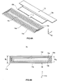
- Fig. 3(A) is a perspective view of the antenna substrate 11 in which the magnetic sheet 13 is inserted on the xy plane
- Fig. 3(B) is a cross-sectional view of the antenna substrate 11 in which the magnetic sheet 13 is inserted on the xy plane.
- the magnetic sheet 13 is inserted into the center portion 11c of the antenna coil 11a formed on the antenna substrate 11 in such a manner that on the upstream side of the proceeding direction of the magnetic field oriented by the metal plate 133a that is opposed to the reader writer 120, the magnetic sheet 13 is disposed so as to be positioned closer to the reader writer 120 side than the antenna coil 11 a and on the downstream side in the proceeding direction of this oriented magnetic field, the antenna coil 11a is disposed so as to be positioned closer to reader writer 120 side than the magnetic sheet 13.
- the antenna substrate 11 is prepared as a flexible printed substrate, a rigid printed substrate, or the like, as described above, and in particular, by using the flexible printed substrate, a cut-out portion is easily formed in the center portion of the antenna coil 11 a, and the magnetic sheet 13 is easily inserted into this cut-out portion.
- the antenna module 1a is preferably formed into the antenna substrate 11 by using a flexible printed substrate in this manner. Moreover, by using the flexible printed substrate, this antenna module 1 a can be easily produced.
- the antenna module 1a is designed such that by disposing the magnetic sheet 13 so as to be positioned closer to the reader writer 120 side than the antenna coil 11 a on the upstream side in the proceeding direction of the magnetic field oriented by the metal plate 133a that is made face to face to the reader writer 120, while disposing the antenna coil 11 a so as to be positioned closer to the reader writer 120 side than the magnetic sheet 13 on the downstream side in the proceeding direction of the magnetic field thus oriented, the magnetic field generated in the gap 132 can be effectively drawn into the antenna coil 11a.
- the antenna module 1a has a structure in which the antenna coil 11a is wound around so as to allow its opening portion, that is, the center portion 11c thereof, to be positioned in the gap 132, it becomes possible to downsize the casing 131 when assembled into an electronic apparatus, such as a portable telephone 130.
- the reason why the magnetic field generated in the gap 132 is allowed to be effectively drawn in the antenna coil 11a is that by disposing the magnetic sheet 13 as described above, a magnetic field component, which is directed from the end portion 133b of the metal plate 133a toward the inner circumferential wall 131a of the casing 131, is allowed to effectively pass through the opening portion of the antenna coil 11 a.
- the antenna module 1a is designed such that, as shown in Fig. 4(A) and Fig. 4(B) , in the y-axis direction in which the magnetic sheet 13 having a virtually T-letter shape is inserted into the center portion 11c of the antenna coil 11a, the magnetic sheet 13 is inserted in such a manner that the two end portions 13a and 13b thereof are respectively positioned closer to the center portion 11c than the two end portions 11d and 11e of the antenna coil 11a.
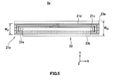
- the magnetic sheet 23 is inserted into the antenna coil 21 a in such a manner that the two end portions 21 d and 21e of the antenna coil 21 a are respectively positioned closer to the center portion 21 c than the two end portions 23a and 23b of the magnetic sheet 23. That is, in the antenna module 2a, in directions in which the magnetic sheet 23 and the antenna coil 21 a are inserted to each other, the width W21 of the antenna coil 21a is made shorter than the width W23 of the magnetic sheet 23.
- a communication characteristic is evaluated at the time when each of the antenna modules 1a, 2a and the reader writer 120 are made face to face with each other, and a relative positional relationship in the x-axis direction is changed.
- the specific evaluation conditions are explained as follows.
- a 461C made by Sony Corporation was used as the reader writer 120.
- the transmission frequency of a magnetic field was set to 13.56 MHz.
- the outside shapes of the antenna coil 11a of the antenna module 1a and the magnetic sheet 23 of the antenna module 2a were respectively fixed to a rectangular shape of 50 mm ⁇ 8.5 mm defined on the xy plane.
- the width W13 of the magnetic sheet 13 is preferably set to virtually 1/2 to less than 1 in the ratio (W13/W11) thereof relative to the width W11 of the antenna coil 11a.
- the antenna module 1 a makes it possible to narrow the entire width of the antenna module by narrowing the width of the magnetic sheet 13 relative to the antenna coil 11a. That is, the antenna module 1a can make the entire module slimmer, while improving the communication characteristic.
- the antenna module 1a is preferably maintained in a state where the magnetic sheet 13 and the antenna coil 11a are mutually superimposed , with an adhesive layer 14 stacked on the surface of at least either the antenna substrate 11 or the magnetic sheet 13 being interposed therebetween, as shown in Fig. 7 .
- Fig. 7(A) shows a state in which the adhesive layer 14 is stacked on the surface of the antenna substrate 11 so as to be virtually coincident with the end portions 13a and 13b of the magnetic sheet 13
- Fig. 7(B) shows a state in which the adhesive layer 14 is stacked on the surface of the antenna substrate 11 so as to be virtually coincident with the end portions 11d and 11e of the antenna coil 11.
- the antenna coil 11a by allowing the antenna coil 11a to satisfy either a condition in which the antenna coil 11a is formed by an antenna substrate 11 having a flexible property or a condition in which the magnetic sheet 13 is flexible, an easily inserting process is achieved so that this structure is preferable from the viewpoint of further reducing the risk of powder dropping. Furthermore, by allowing it to follow one of the surfaces with the adhesive layer 14 being interpolated therebetween even when the degree of plane is biased, this structure becomes more preferable in that the mutually superimposed state can be maintained more positively.
- the antenna module to which the present invention is applied is not necessarily disposed in the gap 132, and for example, one portion of the antenna module 1a may be superimposed on the metal plate 133a that is made face to face with the reader writer 120, and since it is disposed on the outer circumferential portion of the metal plate 133a, a magnetic field oriented by the metal plate 133a can be effectively drawn to the antenna coil 11a.
- the arrangement of the magnetic sheet and the antenna substrate is not limited by an arrangement condition defined by the above-mentioned relationship with the reader writer, and by adopting a structure in which the two ends of the magnetic sheet are located at positions closer to the center portion of the antenna coil than the two ends of the antenna coil in the direction in which the magnetic sheet is inserted to the center portion of the antenna coil, magnetic fluxes can be effectively drawn to the center portion of the antenna coil so that it becomes possible to downsize and to make thin a casing of an electronic apparatus when it is assembled into the electronic apparatus, while maintaining good communication characteristics.
- 1... communication apparatus 1a, 2a... antenna module, 11... antenna substrate, 11 a, 21 a... antenna coil, 11b... terminal unit, 11 c, 21 c... center portion, 11d, 11e, 13a, 13b, 21d, 21e, 23a, 23b... end portion, 12... communication processing unit, 13, 23... magnetic sheet, 14... adhesive layer, 100... radio communication system, 120... reader writer, 121... antenna, 122... control substrate, 130... portable telephone, 131... casing, 131a... inner circumferential wall, 132... gap, 133 ... battery pack, 133a... metal plate, 133b... end portion
Landscapes
- Physics & Mathematics (AREA)
- Engineering & Computer Science (AREA)
- Electromagnetism (AREA)
- Computer Hardware Design (AREA)
- Microelectronics & Electronic Packaging (AREA)
- General Physics & Mathematics (AREA)
- Theoretical Computer Science (AREA)
- Support Of Aerials (AREA)
- Telephone Set Structure (AREA)
- Details Of Aerials (AREA)
- Near-Field Transmission Systems (AREA)
Abstract

Description
- The present invention relates to an antenna apparatus that is assembled into an electronic apparatus and can be communicated upon receipt of a magnetic field transmitted from a transmitter, and a communication apparatus.
- The present application asserts priority rights based on
JP Patent Application 2011-260640 - In electronic apparatuses such as portable telephones, an antenna module for an RFID (Radio Frequency Identification) has been used for installing a function for near non-contact communication therein.
- This antenna module carries out a communication by utilizing an inductive coupling with an antenna coil mounted on a transmitter such as a reader writer. That is, by allowing its antenna coil to receive a magnetic field from the reader writer, this antenna module converts it into electric power and makes it possible to drive an IC that functions as a communication processing unit.
- In order to positively carry out communication, the antenna module needs to receive a magnetic flux of a predetermined value or more by the antenna coil from the reader writer. For this reason, an antenna module according to a conventional example installs a loop coil in a casing of the portable telephone, and receives the magnetic flux from the reader writer by using this coil.
- However, in the antenna module assembled into an electronic apparatus such as a portable telephone, since the magnetic flux from the reader writer is repelled by an eddy current that is generated by metals for use in substrates, battery packs or the like inside the apparatus, when they receive a magnetic field from the reader writer, the magnetic flux reaching the loop coil becomes smaller. Since the magnetic flux reaching the loop coil becomes smaller in this manner, the antenna module requires a loop coil having a certain size for collecting required magnetic fluxes, and it is further necessary to use a magnetic sheet so as to increase the magnetic fluxes.
- As described above, the magnetic flux from the reader writer is repelled by the eddy current flowing through the substrate of the electronic apparatus such as a portable telephone; however, on the surface of the casing in the electronic apparatus, there is a magnetic field component directed in the in-plane direction of the substrate, and
Patent Document 1 has proposed an apparatus in which, by receiving this component, a function for an antenna is exerted. More specifically,Patent Document 1 has proposed an antenna structure in which a coil is wound around a ferrite core so as to reduce the occupied area of the coil. - PTL 1: Japanese Patent Application Laid-Open No.
2008-35464 - As described above, in an electronic apparatus such as a portable telephone, since the substrates or the like that transmit electricity comparatively well are used, a magnetic field is repelled by an eddy current generated in the substrate that has received the magnetic field. For example, when considering the casing surface of the portable telephone, the magnetic field that is applied from the reader writer tends to become stronger on the outer peripheral portion of the casing surface, while it tends to become weaker in the vicinity of the center of the casing surface.
- In the case of an antenna using a normal loop coil, the opening portion of the loop coil is positioned in the center portion of the portable telephone that is not allowed to receive the magnetic field passing through the above-mentioned outer peripheral portion of the casing surface so much. For this reason, in the case of an antenna using the normal loop coil, its efficiency for receiving a magnetic field becomes poor.
- Moreover, in the case of an antenna structure in which a coil is wound around a ferrite core described in
Patent Document 1 and the coil is assembled into the portable telephone, since the cross section of the ferrite core corresponds to the area for use in collecting a magnetic flux, the thickness of the ferrite core of, for example, 1 mm or more is required, with the result that the casing of the portable telephone has a comparatively thick structure. Therefore, this structure is difficult to be installed inside a portable telephone having a comparatively thin size. Moreover, in the case when this antenna module is assembled on the rear side of a liquid crystal display installed on a folding portable telephone, since the thinness thereof is also required, it is difficult that the antenna structure disclosed inPatent Document 1 secures the required space. - The present invention has been proposed in view of these circumstances, and its object is to provide a communication apparatus which, while maintaining a communication characteristic, makes it possible to downsize a casing of an electronic apparatus when assembled into the electronic apparatus.
- In order to solve the above-mentioned problems, the present invention relates to an antenna apparatus that is assembled into an electronic apparatus and can be communicated upon receipt of a magnetic field transmitted from a transmitter, and the antenna apparatus is provided with an antenna substrate on which an antenna coil that is inductively coupled to the transmitter is formed, and a magnetic sheet that draws a magnetic field transmitted from the transmitter into the antenna coil, and this structure is characterized in that since the magnetic sheet is inserted into the center portion of the antenna coil formed on the antenna substrate, the two ends of the magnetic sheet are located at positions closer to the center portion in the inserting direction than the two ends of the antenna coil in the inserting direction.
- Moreover, the present invention relates to a communication apparatus that can be communicated upon receipt of a magnetic field transmitted from a transmitter, and the communication apparatus is characterized by having an antenna substrate on which an antenna coil that is inductively coupled to the transmitter is formed, a magnetic sheet that draws a magnetic field transmitted from the transmitter into the antenna coil, and a communication processing unit that is driven by an electric current flowing through the antenna coil, and carries out communication between the transmitter, and since the magnetic sheet is inserted into the center portion of the antenna coil formed on the antenna substrate, the antenna coil and the magnetic sheet are mutually superimposed in a manner so as to satisfy both of an arrangement condition in which the magnetic sheet is positioned closer to the transmitter than the antenna coil on the upstream side in the proceeding direction of the magnetic field oriented by the casing surface that is opposed to the transmitter and an arrangement condition in which the antenna coil is positioned closer to the transmitter side than the magnetic sheet on the downstream side in the oriented proceeding direction, and the magnetic sheet is characterized in that in the inserting direction into the center portion of the antenna coil, two ends of the magnetic sheet are positioned closer to a center portion than the two ends of the antenna coil.
- In the present invention, in the inserting direction in which the magnetic sheet is inserted into the center portion of the antenna coil, since the two ends of the magnetic sheet are located at positions closer to the center portion than the two ends of the antenna coil so as to efficiently draw a magnetic flux to the center portion of the antenna coil, it is possible to downsize and to make thin a casing of an electronic apparatus, while maintaining good communication characteristic, when the communication device is assembled into the electronic apparatus. Brief Description of Drawings
-
-
Figure 1 is a drawing for use in explaining a configuration of a radio communication system in which a radio communication apparatus to which the present invention applied is assembled. -
Figure 2 is a drawing for use in explaining a configuration of the communication apparatus that is disposed inside a casing of a portable telephone. -
Figure 3(A) is a perspective view showing an antenna module, andFigure 3(B) is a cross-sectional view of the antenna module. -
Figures 4(A) and 4(B) are drawings for use in explaining a positional relationship between the two ends of a magnetic sheet and the two ends of an antenna coil in the antenna module to which the present invention is applied. -
Figure 5 is a drawing for use in explaining a positional relationship between the two ends of a magnetic sheet and the two ends of an antenna coil in an antenna module according to a comparative example. -
Figure 6 is a drawing for use in explaining a change in communication characteristics in the case when a difference between the widths of the antenna coil and the magnetic sheet is changed. -
Figure 7(A) is a drawing that shows a configuration in which a sticker layer is stacked on a surface of an antenna substrate so as to be virtually coincident with the width of the magnetic sheet, andFigure 7(B) is a drawing that shows a configuration in which a sticker layer is stacked on a surface of theantenna substrate 11 so as to be virtually coincident with the width of the antenna coil. - Referring to Figures, the following description will discuss embodiments for carrying out the present invention in detail. Additionally, the present invention is not intended to be limited by the following embodiments, and it is needless to say that various modifications may be made therein within a scope without departing from the gist of the present invention.
- The communication apparatus to which the present invention is applied is an apparatus that is assembled into an electronic apparatus and can be communicated upon receipt of a magnetic field transmitted from a transmitter, and is incorporated into a
radio communication system 100 for an RFID (Radio Frequency Identification), for example, as shown inFig. 1 , and used. - The
radio communication system 100 is composed of acommunication apparatus 1 to which the present invention is applied and areader writer 120 that accesses thecommunication apparatus 1. In this case, thecommunication apparatus 1 and thereader writer 120 are supposed to be disposed so as to be made face to face with each other on the xy plane of a three-dimensional orthogonal coordinate system xyz. - The
reader writer 120 functions as a transmitter for transmitting a magnetic field in the z-axis direction to thecommunication apparatus 1 that is made face to face with each other thereto on the xy plane, and is more specifically provided with anantenna 121 that transmits a magnetic field toward thecommunication apparatus 1 and acontrol substrate 122 that communicates with thecommunication apparatus 1 that is inductively coupled thereto through theantenna 121. - That is, the
reader writer 120 is provided with thecontrol substrate 122 that is electrically connected to theantenna 121. On thecontrol substrate 122, a control circuit, which is made of electronic parts, such as one or a plurality of electronic integrated circuit chips, is assembled. The control circuit executes various processes based upon data received from thecommunication apparatus 1. For example, when transmitting data to thecommunication apparatus 1, the control circuit encodes data, and based upon the encoded data, modulates a carrier wave having a predetermined frequency (for example, 13.56 MHz), amplifies a modulation signal thus modulated, and drives theantenna 121 by using the amplified modulation signal. Moreover, when reading out data from thecommunication apparatus 1, the control circuit amplifies the modulation signal of data received by theantenna 121, demodulates the modulation signal of the amplified data, and decodes the data thus demodulated. Additionally, in the control circuit, an encoding system and a modulation system generally used in a reader writer are adopted, and, for example, a Manchester encoding system and an ASK (Amplitude Shift Keying) modulation system are used. - The
communication apparatus 1 is provided with anantenna module 1 a having anantenna substrate 11 in which anantenna coil 11 a, which is assembled into acasing 131 of a portable telephone 130 disposed so as to be made face to face with, for example, thereader writer 120 on the xy plane, and can be communicated with thereader writer 120 inductively coupled thereto, is assembled, and acommunication processing unit 12 that is driven by an electric current flowing through theantenna coil 11a, and communicates with thereader writer 120. - On the
antenna substrate 11, theantenna coil 11a formed by patterning a flexible lead line, such as, for example, a flexible printed substrate, and aterminal unit 11b that electrically connects theantenna coil 11 a with thecommunication processing unit 12, are assembled. - Upon receipt of a magnetic field transmitted from the
reader writer 120, theantenna coil 11a is magnetically coupled with thereader writer 120 by inductive coupling, receives a modulated electromagnetic wave, and supplies the received signal to thecommunication processing unit 12 through theterminal unit 11b. - The
communication processing unit 12 is driven by an electric current flowing through theantenna coil 11 a, and communicates with thereader writer 120. More specifically, thecommunication processing unit 12 demodulates the modulation signal received, decodes the demodulated data, and writes the decoded data in the inner memory possessed by thecommunication processing unit 12. Moreover, thecommunication processing unit 12 reads out data to be transmitted to thereader writer 120 from the inner memory, encodes the data thus read out, modulates a carrier wave based upon the encoded data, and transmits the modulated electric wave to thereader writer 120 through theantenna coil 11a magnetically coupled thereto by inductive coupling. - In the
radio communication system 100 having the above-mentioned configuration, the following description will discuss the configuration of theantenna module 1 a. - From the viewpoints of downsizing an electronic apparatus when assembled into the electronic apparatus such as a portable telephone 130, and of realizing a good communication characteristic between the
reader writer 120, theantenna coil 11a of theantenna module 1a is disposed in agap 132 between abattery pack 133 installed inside thecasing 131 of the portable telephone 130 and an innercircumferential wall 131 a of thecasing 131, for example, on the xy plane of the three-dimensional orthogonal coordinate system xyz as shown inFig. 2(A) . - Additionally, the
antenna module 1a may be installed not only in thegap 132 between thebattery pack 133 and the innercircumferential wall 131a of thecasing 131, as described above, but also in a gap between a conductor disposed inside thecasing 131, such as, for example, an integrated circuit substrate and the inner circumferential wall of the casing. In the present embodiment, explanations will be made on the assumption that the antenna module is disposed in a gap between theend portion 133b of themetal plate 133a that is made face to face with thereader writer 120 that forms the metal casing of thebattery pack 133, as shown inFig. 2(B) , and the innercircumferential wall 131a of thecasing 131, as a plate-shaped conductor, for convenience of explanation. - In this case, as shown in the cross-sectional view in
Fig. 2(B) , since themetal plate 133a serving as the metal casing of thebattery pack 133 disposed in the portable telephone 130, that is, as the specific example of the casing surface that is made face to face with thereader writer 120, allows electricity to pass therethrough comparatively well, an eddy current is generated when an AC magnetic field is applied thereto from the outside, with the result that the magnetic field is repelled therefrom. By making an examination about the magnetic field distribution upon application of the AC magnetic field from the outside in this manner, a characteristic is found in which the magnetic field is strong at theend portion 133b of themetal plate 133a of thebattery pack 133 that is made face to face with thereader writer 120. More specifically, the magnetic field in thegap 132 in which theantenna module 1a is disposed has a greater component in the y-axis direction. In order to effectively draw such a magnetic field having a greater component in the y-axis direction into theantenna coil 11a, theantenna module 1a is provided with amagnetic sheet 13 that is disposed as shown inFig. 3 , and superimposed on theantenna coil 11 a. - Here,
Fig. 3(A) is a perspective view of theantenna substrate 11 in which themagnetic sheet 13 is inserted on the xy plane, andFig. 3(B) is a cross-sectional view of theantenna substrate 11 in which themagnetic sheet 13 is inserted on the xy plane. - As shown in
Fig. 3(B) , in theantenna module 1a, themagnetic sheet 13 is inserted into thecenter portion 11c of theantenna coil 11a formed on theantenna substrate 11 in such a manner that on the upstream side of the proceeding direction of the magnetic field oriented by themetal plate 133a that is opposed to thereader writer 120, themagnetic sheet 13 is disposed so as to be positioned closer to thereader writer 120 side than theantenna coil 11 a and on the downstream side in the proceeding direction of this oriented magnetic field, theantenna coil 11a is disposed so as to be positioned closer toreader writer 120 side than themagnetic sheet 13. - In this case, the
antenna substrate 11 is prepared as a flexible printed substrate, a rigid printed substrate, or the like, as described above, and in particular, by using the flexible printed substrate, a cut-out portion is easily formed in the center portion of theantenna coil 11 a, and themagnetic sheet 13 is easily inserted into this cut-out portion. From the view point of easily inserting themagnetic sheet 13 into theantenna substrate 11, theantenna module 1a is preferably formed into theantenna substrate 11 by using a flexible printed substrate in this manner. Moreover, by using the flexible printed substrate, thisantenna module 1 a can be easily produced. - In this manner, the
antenna module 1a is designed such that by disposing themagnetic sheet 13 so as to be positioned closer to thereader writer 120 side than theantenna coil 11 a on the upstream side in the proceeding direction of the magnetic field oriented by themetal plate 133a that is made face to face to thereader writer 120, while disposing theantenna coil 11 a so as to be positioned closer to thereader writer 120 side than themagnetic sheet 13 on the downstream side in the proceeding direction of the magnetic field thus oriented, the magnetic field generated in thegap 132 can be effectively drawn into theantenna coil 11a. - Moreover, since the
antenna module 1a has a structure in which theantenna coil 11a is wound around so as to allow its opening portion, that is, thecenter portion 11c thereof, to be positioned in thegap 132, it becomes possible to downsize thecasing 131 when assembled into an electronic apparatus, such as a portable telephone 130. - The reason why the magnetic field generated in the
gap 132 is allowed to be effectively drawn in theantenna coil 11a is that by disposing themagnetic sheet 13 as described above, a magnetic field component, which is directed from theend portion 133b of themetal plate 133a toward the innercircumferential wall 131a of thecasing 131, is allowed to effectively pass through the opening portion of theantenna coil 11 a. - Moreover, from the viewpoints of both of achieving a good communication characteristic as indicated by a performance evaluation to be described later and downsizing, the
antenna module 1a is designed such that, as shown inFig. 4(A) and Fig. 4(B) , in the y-axis direction in which themagnetic sheet 13 having a virtually T-letter shape is inserted into thecenter portion 11c of theantenna coil 11a, themagnetic sheet 13 is inserted in such a manner that the twoend portions center portion 11c than the twoend portions antenna coil 11a. In this manner, in theantenna module 1 a, in the direction in which themagnetic sheet 13 and theantenna coil 11 a are inserted to each other, by making the width W13 of themagnetic sheet 13 shorter than the width W11 of theantenna coil 11a, it is possible to realize a communication characteristic better than that of anantenna module 2a according to a comparative example, for example, shown inFig. 5 . - As shown in
Fig. 5 , in theantenna module 2a according to the comparative example, in the y-axis direction in which themagnetic sheet 23 is inserted into thecenter portion 21 c of theantenna coil 21 a, themagnetic sheet 23 is inserted into theantenna coil 21 a in such a manner that the twoend portions antenna coil 21 a are respectively positioned closer to thecenter portion 21 c than the twoend portions magnetic sheet 23. That is, in theantenna module 2a, in directions in which themagnetic sheet 23 and theantenna coil 21 a are inserted to each other, the width W21 of theantenna coil 21a is made shorter than the width W23 of themagnetic sheet 23. - First, as a performance evaluation, a communication characteristic is evaluated at the time when each of the
antenna modules reader writer 120 are made face to face with each other, and a relative positional relationship in the x-axis direction is changed. - The specific evaluation conditions are explained as follows. A 461C made by Sony Corporation was used as the
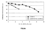
reader writer 120. The transmission frequency of a magnetic field was set to 13.56 MHz. Moreover, the outside shapes of theantenna coil 11a of theantenna module 1a and themagnetic sheet 23 of theantenna module 2a were respectively fixed to a rectangular shape of 50 mm × 8.5 mm defined on the xy plane. - In this manner, with W11 and W23 being fixed to 8.5 mm, changes in communication distance when the difference between the widths of the antenna coil and the magnetic sheet, that is, W11 - W13, was changed from 0 mm to 8.5 mm, and when the difference therebetween, that is, W23 - W21, was changed from 0 mm to 3 mm, were shown in
Fig. 6 . - As clearly indicated by the results shown in
Fig. 6 , in theantenna module 1a, by making the width W13 of themagnetic sheet 13 shorter than the width W11 of theantenna coil 11 a in directions in which themagnetic sheet 13 and theantenna coil 11a are inserted to each other, a superior communication characteristic can be realized. Moreover, when W11 - W13 becomes greater than 4 mm, the communication distance becomes shorter. Consequently, the width W13 of themagnetic sheet 13 is preferably set to virtually 1/2 to less than 1 in the ratio (W13/W11) thereof relative to the width W11 of theantenna coil 11a. - In this manner, the
antenna module 1 a makes it possible to narrow the entire width of the antenna module by narrowing the width of themagnetic sheet 13 relative to theantenna coil 11a. That is, theantenna module 1a can make the entire module slimmer, while improving the communication characteristic. - Moreover, the
antenna module 1a is preferably maintained in a state where themagnetic sheet 13 and theantenna coil 11a are mutually superimposed , with anadhesive layer 14 stacked on the surface of at least either theantenna substrate 11 or themagnetic sheet 13 being interposed therebetween, as shown inFig. 7 . In this case,Fig. 7(A) shows a state in which theadhesive layer 14 is stacked on the surface of theantenna substrate 11 so as to be virtually coincident with theend portions magnetic sheet 13, andFig. 7(B) shows a state in which theadhesive layer 14 is stacked on the surface of theantenna substrate 11 so as to be virtually coincident with theend portions antenna coil 11. - With this structure, in the
antenna module 1 a, even when the end portions of themagnetic sheet 13 are cracked to cause a powder drop, the dropped powder can be received by theadhesive layer 14, so that it is consequently possible to prevent foreign matters from scattering in the portable telephone 130. In particular, in the case of using ferrite having a comparatively high magnetic characteristic as themagnetic sheet 13, since it is a sintered member and is easily cracked by an externally applied force to cause a powder drop, this structure is more suitably applied thereto. Moreover, from the viewpoint of efficiently preventing the powder drop of themagnetic sheet 13, as shown inFig. 7(B) , it is in particular preferable to stack theadhesive layer 14 on the surface of theantenna substrate 11 so as to make the width thereof virtually coincident with the width of theantenna coil 11. - Moreover, by allowing the
antenna coil 11a to satisfy either a condition in which theantenna coil 11a is formed by anantenna substrate 11 having a flexible property or a condition in which themagnetic sheet 13 is flexible, an easily inserting process is achieved so that this structure is preferable from the viewpoint of further reducing the risk of powder dropping. Furthermore, by allowing it to follow one of the surfaces with theadhesive layer 14 being interpolated therebetween even when the degree of plane is biased, this structure becomes more preferable in that the mutually superimposed state can be maintained more positively. - Additionally, the antenna module to which the present invention is applied is not necessarily disposed in the
gap 132, and for example, one portion of theantenna module 1a may be superimposed on themetal plate 133a that is made face to face with thereader writer 120, and since it is disposed on the outer circumferential portion of themetal plate 133a, a magnetic field oriented by themetal plate 133a can be effectively drawn to theantenna coil 11a. Moreover, in the antenna module to which the present invention is applied, the arrangement of the magnetic sheet and the antenna substrate is not limited by an arrangement condition defined by the above-mentioned relationship with the reader writer, and by adopting a structure in which the two ends of the magnetic sheet are located at positions closer to the center portion of the antenna coil than the two ends of the antenna coil in the direction in which the magnetic sheet is inserted to the center portion of the antenna coil, magnetic fluxes can be effectively drawn to the center portion of the antenna coil so that it becomes possible to downsize and to make thin a casing of an electronic apparatus when it is assembled into the electronic apparatus, while maintaining good communication characteristics. Reference Signs List - 1... communication apparatus, 1a, 2a... antenna module, 11... antenna substrate, 11 a, 21 a... antenna coil, 11b... terminal unit, 11 c, 21 c... center portion, 11d, 11e, 13a, 13b, 21d, 21e, 23a, 23b... end portion, 12... communication processing unit, 13, 23... magnetic sheet, 14... adhesive layer, 100... radio communication system, 120... reader writer, 121... antenna, 122... control substrate, 130... portable telephone, 131... casing, 131a... inner circumferential wall, 132... gap, 133 ... battery pack, 133a... metal plate, 133b... end portion
Claims (8)
- An antenna apparatus, which is assembled into an electronic apparatus and can be communicated upon receipt of a magnetic field transmitted from a transmitter, comprising:an antenna substrate on which an antenna coil that is inductively coupled to the transmitter is formed; anda magnetic sheet for use in drawing the magnetic field transmitted from the transmitter to the antenna coil,wherein the magnetic sheet is inserted into a center portion of the antenna coil formed on the antenna substrate, with two ends of the magnetic sheet being located at positions closer to the center portion than two ends of the antenna coil in the inserting direction thereof.
- The antenna apparatus according to claim 1, wherein since the magnetic sheet is inserted into a center portion of the antenna coil formed on the antenna substrate, the antenna coil and the magnetic sheet are mutually superimposed in a manner so as to satisfy both of an arrangement condition in which the magnetic sheet is positioned closer to the transmitter side than the antenna coil on the upstream side in the proceeding direction of the magnetic field oriented by a casing surface that is opposed to the transmitter and an arrangement condition in which the antenna coil is positioned closer to the transmitter side than the magnetic sheet on the downstream side in the oriented proceeding direction.
- The antenna apparatus according to claim 1, wherein in a direction in which the magnetic sheet is inserted into the center portion of the antenna coil, the magnetic sheet has a width having a ratio relative to the width of the antenna coil of virtually 1/2 to less than 1.
- The antenna apparatus according to claim 1, wherein the magnetic sheet and the antenna coil are maintained in a state in which the magnetic sheet and the antenna coil are mutually superimposed with an adhesive layer being interposed therebetween.
- The antenna apparatus according to claim 1, wherein at least either one of conditions in which the antenna coil is formed by an antenna substrate having a pliable property or in which the magnetic sheet has a flexible property is satisfied.
- A communication apparatus, which can be communicated upon receipt of a magnetic field transmitted from a transmitter, comprising:an antenna substrate on which an antenna coil that is inductively coupled to the transmitter is formed;a magnetic sheet for use in drawing a magnetic field transmitted from the transmitter to the antenna coil; anda communication processing unit that is driven by an electric current flowing through the antenna coil, and carries out communication between the transmitter,wherein since the magnetic sheet is inserted into a center portion of the antenna coil formed on the antenna substrate, the antenna coil and the magnetic sheet are mutually superimposed on each other in a manner so as to satisfy both of an arrangement condition in which the magnetic sheet is positioned closer to the transmitter side than the antenna coil on the upstream side in the proceeding direction of the magnetic field oriented by a casing surface that is opposed to the transmitter and an arrangement condition in which the antenna coil is positioned closer to the transmitter side than the magnetic sheet on the downstream side in the oriented proceeding direction, andwherein the magnetic sheet is inserted such that in the inserting direction into the center portion of the antenna coil, two ends of the magnetic sheet are located at positions closer to the center portion than two ends of the antenna coil.
- The communication apparatus according to claim 6, wherein the antenna coil is wound in such a manner that an opening of the antenna coil is positioned in a gap between an end portion of a conductor that is made face to face with the transmitter inside a casing of the electronic apparatus and an inner circumferential wall of the casing.
- The communication apparatus according to claim 6, wherein the antenna substrate and the magnetic sheet are disposed on an outer circumferential portion of the casing surface that is made face to face with the transmitter.
Applications Claiming Priority (2)
| Application Number | Priority Date | Filing Date | Title |
|---|---|---|---|
| JP2011260640A JP2013115648A (en) | 2011-11-29 | 2011-11-29 | Antenna device and communication device |
| PCT/JP2012/079631 WO2013080804A1 (en) | 2011-11-29 | 2012-11-15 | Antenna apparatus and communication apparatus |
Publications (3)
| Publication Number | Publication Date |
|---|---|
| EP2787575A1 true EP2787575A1 (en) | 2014-10-08 |
| EP2787575A4 EP2787575A4 (en) | 2015-07-29 |
| EP2787575B1 EP2787575B1 (en) | 2017-01-11 |
Family
ID=48535270
Family Applications (1)
| Application Number | Title | Priority Date | Filing Date |
|---|---|---|---|
| EP12854142.2A Active EP2787575B1 (en) | 2011-11-29 | 2012-11-15 | Antenna apparatus and communication apparatus |
Country Status (6)
| Country | Link |
|---|---|
| US (1) | US20140320355A1 (en) |
| EP (1) | EP2787575B1 (en) |
| JP (1) | JP2013115648A (en) |
| CN (1) | CN103947043B (en) |
| TW (1) | TWI606636B (en) |
| WO (1) | WO2013080804A1 (en) |
Families Citing this family (9)
| Publication number | Priority date | Publication date | Assignee | Title |
|---|---|---|---|---|
| KR101502391B1 (en) * | 2014-02-28 | 2015-03-13 | 한국과학기술연구원 | Wideband antenna using ferrite |
| JP6461577B2 (en) * | 2014-11-28 | 2019-01-30 | 東洋アルミニウム株式会社 | Inlet antenna for RFID, RFID and manufacturing method thereof |
| JP2016158208A (en) * | 2015-02-26 | 2016-09-01 | デクセリアルズ株式会社 | Antenna device and electronic apparatus |
| JP6627252B2 (en) * | 2015-04-28 | 2020-01-08 | Tdk株式会社 | Antenna device |
| CN105552526B (en) * | 2016-02-26 | 2019-05-21 | Oppo广东移动通信有限公司 | Mobile terminal |
| JP2018201165A (en) * | 2017-05-29 | 2018-12-20 | 株式会社リコー | Antenna device and method for manufacturing the same |
| CN108987945B (en) | 2018-07-24 | 2020-08-04 | 维沃移动通信有限公司 | a terminal device |
| CN108987944B (en) * | 2018-07-24 | 2021-04-23 | 维沃移动通信有限公司 | a terminal device |
| TWI836460B (en) * | 2022-06-07 | 2024-03-21 | 韋僑科技股份有限公司 | Radio frequency identification device |
Family Cites Families (14)
| Publication number | Priority date | Publication date | Assignee | Title |
|---|---|---|---|---|
| KR20040037127A (en) * | 2001-09-28 | 2004-05-04 | 미쓰비시 마테리알 가부시키가이샤 | Antenna coil and rfid-use tag using it, transponder-use antenna |
| JP4232474B2 (en) * | 2002-09-27 | 2009-03-04 | ソニー株式会社 | Electronic equipment with communication function |
| JP4414942B2 (en) * | 2005-06-30 | 2010-02-17 | ソニーケミカル&インフォメーションデバイス株式会社 | Antenna device |
| JP4887794B2 (en) * | 2006-01-18 | 2012-02-29 | 株式会社村田製作所 | Portable electronic devices |
| JP3933191B1 (en) | 2006-03-13 | 2007-06-20 | 株式会社村田製作所 | Portable electronic devices |
| JP2008040904A (en) * | 2006-08-08 | 2008-02-21 | Hitachi Ltd | RFID tag and reading method thereof |
| JP4917484B2 (en) * | 2006-06-16 | 2012-04-18 | ニッタ株式会社 | Magnetic sheet, antenna device using the same, and electronic information transmission device |
| JP4883125B2 (en) * | 2009-04-03 | 2012-02-22 | 株式会社村田製作所 | antenna |
| JP4978657B2 (en) * | 2009-05-08 | 2012-07-18 | 株式会社村田製作所 | Antenna device |
| KR101226158B1 (en) * | 2009-09-25 | 2013-01-24 | 가부시키가이샤 무라타 세이사쿠쇼 | Antenna device and communication terminal device |
| JP5487919B2 (en) * | 2009-12-01 | 2014-05-14 | 株式会社村田製作所 | Magnetic material antenna and portable terminal |
| JP4935964B2 (en) * | 2009-12-24 | 2012-05-23 | 株式会社村田製作所 | Communication terminal |
| WO2011077877A1 (en) * | 2009-12-24 | 2011-06-30 | 株式会社村田製作所 | Antenna and handheld terminal |
| JP5135450B2 (en) * | 2010-03-31 | 2013-02-06 | デクセリアルズ株式会社 | Antenna device, communication device |
-
2011
- 2011-11-29 JP JP2011260640A patent/JP2013115648A/en active Pending
-
2012
- 2012-11-15 CN CN201280058696.2A patent/CN103947043B/en active Active
- 2012-11-15 WO PCT/JP2012/079631 patent/WO2013080804A1/en not_active Ceased
- 2012-11-15 EP EP12854142.2A patent/EP2787575B1/en active Active
- 2012-11-15 US US14/361,549 patent/US20140320355A1/en not_active Abandoned
- 2012-11-21 TW TW101143355A patent/TWI606636B/en active
Also Published As
| Publication number | Publication date |
|---|---|
| TW201334283A (en) | 2013-08-16 |
| EP2787575B1 (en) | 2017-01-11 |
| US20140320355A1 (en) | 2014-10-30 |
| CN103947043B (en) | 2017-06-09 |
| TWI606636B (en) | 2017-11-21 |
| WO2013080804A1 (en) | 2013-06-06 |
| EP2787575A4 (en) | 2015-07-29 |
| JP2013115648A (en) | 2013-06-10 |
| CN103947043A (en) | 2014-07-23 |
Similar Documents
| Publication | Publication Date | Title |
|---|---|---|
| EP2787575B1 (en) | Antenna apparatus and communication apparatus | |
| KR101944146B1 (en) | Antenna apparatus, communication apparatus, and antenna apparatus manufacturing method | |
| US9748636B2 (en) | Antenna device and electronic apparatus | |
| US8849195B2 (en) | Antenna device and communication device | |
| US10547111B2 (en) | Method for manufacturing antenna device, and antenna device | |
| EP2693562B1 (en) | Antenna apparatus and communication apparatus | |
| TWI693738B (en) | Antenna device and electronic equipment | |
| US20160198028A1 (en) | Antenna device and electronic apparatus | |
| CN105103373B (en) | Antenna assembly and electronic equipment | |
| CN107851899A (en) | Antenna assembly and electronic equipment | |
| US20160268674A1 (en) | Antenna device and electronic apparaus | |
| US9954283B2 (en) | Antenna device and electronic apparatus | |
| JP6282692B2 (en) | Communication device | |
| JP2013125981A (en) | Antenna device and communication device |
Legal Events
| Date | Code | Title | Description |
|---|---|---|---|
| PUAI | Public reference made under article 153(3) epc to a published international application that has entered the european phase |
Free format text: ORIGINAL CODE: 0009012 |
|
| 17P | Request for examination filed |
Effective date: 20140616 |
|
| AK | Designated contracting states |
Kind code of ref document: A1 Designated state(s): AL AT BE BG CH CY CZ DE DK EE ES FI FR GB GR HR HU IE IS IT LI LT LU LV MC MK MT NL NO PL PT RO RS SE SI SK SM TR |
|
| DAX | Request for extension of the european patent (deleted) | ||
| RA4 | Supplementary search report drawn up and despatched (corrected) |
Effective date: 20150626 |
|
| RIC1 | Information provided on ipc code assigned before grant |
Ipc: H01Q 7/06 20060101AFI20150622BHEP Ipc: H01Q 1/38 20060101ALI20150622BHEP Ipc: G06K 19/07 20060101ALI20150622BHEP Ipc: H01Q 1/24 20060101ALI20150622BHEP Ipc: H01Q 1/22 20060101ALI20150622BHEP Ipc: G06K 19/077 20060101ALI20150622BHEP |
|
| GRAP | Despatch of communication of intention to grant a patent |
Free format text: ORIGINAL CODE: EPIDOSNIGR1 |
|
| INTG | Intention to grant announced |
Effective date: 20160714 |
|
| STAA | Information on the status of an ep patent application or granted ep patent |
Free format text: STATUS: GRANT OF PATENT IS INTENDED |
|
| GRAS | Grant fee paid |
Free format text: ORIGINAL CODE: EPIDOSNIGR3 |
|
| GRAA | (expected) grant |
Free format text: ORIGINAL CODE: 0009210 |
|
| STAA | Information on the status of an ep patent application or granted ep patent |
Free format text: STATUS: THE PATENT HAS BEEN GRANTED |
|
| AK | Designated contracting states |
Kind code of ref document: B1 Designated state(s): AL AT BE BG CH CY CZ DE DK EE ES FI FR GB GR HR HU IE IS IT LI LT LU LV MC MK MT NL NO PL PT RO RS SE SI SK SM TR |
|
| REG | Reference to a national code |
Ref country code: GB Ref legal event code: FG4D |
|
| REG | Reference to a national code |
Ref country code: CH Ref legal event code: EP |
|
| REG | Reference to a national code |
Ref country code: AT Ref legal event code: REF Ref document number: 862054 Country of ref document: AT Kind code of ref document: T Effective date: 20170115 |
|
| REG | Reference to a national code |
Ref country code: IE Ref legal event code: FG4D |
|
| REG | Reference to a national code |
Ref country code: DE Ref legal event code: R096 Ref document number: 602012027869 Country of ref document: DE |
|
| REG | Reference to a national code |
Ref country code: LT Ref legal event code: MG4D |
|
| REG | Reference to a national code |
Ref country code: NL Ref legal event code: MP Effective date: 20170111 |
|
| REG | Reference to a national code |
Ref country code: AT Ref legal event code: MK05 Ref document number: 862054 Country of ref document: AT Kind code of ref document: T Effective date: 20170111 |
|
| PG25 | Lapsed in a contracting state [announced via postgrant information from national office to epo] |
Ref country code: NL Free format text: LAPSE BECAUSE OF FAILURE TO SUBMIT A TRANSLATION OF THE DESCRIPTION OR TO PAY THE FEE WITHIN THE PRESCRIBED TIME-LIMIT Effective date: 20170111 |
|
| PG25 | Lapsed in a contracting state [announced via postgrant information from national office to epo] |
Ref country code: IS Free format text: LAPSE BECAUSE OF FAILURE TO SUBMIT A TRANSLATION OF THE DESCRIPTION OR TO PAY THE FEE WITHIN THE PRESCRIBED TIME-LIMIT Effective date: 20170511 Ref country code: LT Free format text: LAPSE BECAUSE OF FAILURE TO SUBMIT A TRANSLATION OF THE DESCRIPTION OR TO PAY THE FEE WITHIN THE PRESCRIBED TIME-LIMIT Effective date: 20170111 Ref country code: HR Free format text: LAPSE BECAUSE OF FAILURE TO SUBMIT A TRANSLATION OF THE DESCRIPTION OR TO PAY THE FEE WITHIN THE PRESCRIBED TIME-LIMIT Effective date: 20170111 Ref country code: NO Free format text: LAPSE BECAUSE OF FAILURE TO SUBMIT A TRANSLATION OF THE DESCRIPTION OR TO PAY THE FEE WITHIN THE PRESCRIBED TIME-LIMIT Effective date: 20170411 Ref country code: GR Free format text: LAPSE BECAUSE OF FAILURE TO SUBMIT A TRANSLATION OF THE DESCRIPTION OR TO PAY THE FEE WITHIN THE PRESCRIBED TIME-LIMIT Effective date: 20170412 |
|
| PG25 | Lapsed in a contracting state [announced via postgrant information from national office to epo] |
Ref country code: PT Free format text: LAPSE BECAUSE OF FAILURE TO SUBMIT A TRANSLATION OF THE DESCRIPTION OR TO PAY THE FEE WITHIN THE PRESCRIBED TIME-LIMIT Effective date: 20170511 Ref country code: ES Free format text: LAPSE BECAUSE OF FAILURE TO SUBMIT A TRANSLATION OF THE DESCRIPTION OR TO PAY THE FEE WITHIN THE PRESCRIBED TIME-LIMIT Effective date: 20170111 Ref country code: AT Free format text: LAPSE BECAUSE OF FAILURE TO SUBMIT A TRANSLATION OF THE DESCRIPTION OR TO PAY THE FEE WITHIN THE PRESCRIBED TIME-LIMIT Effective date: 20170111 Ref country code: SE Free format text: LAPSE BECAUSE OF FAILURE TO SUBMIT A TRANSLATION OF THE DESCRIPTION OR TO PAY THE FEE WITHIN THE PRESCRIBED TIME-LIMIT Effective date: 20170111 Ref country code: PL Free format text: LAPSE BECAUSE OF FAILURE TO SUBMIT A TRANSLATION OF THE DESCRIPTION OR TO PAY THE FEE WITHIN THE PRESCRIBED TIME-LIMIT Effective date: 20170111 Ref country code: LV Free format text: LAPSE BECAUSE OF FAILURE TO SUBMIT A TRANSLATION OF THE DESCRIPTION OR TO PAY THE FEE WITHIN THE PRESCRIBED TIME-LIMIT Effective date: 20170111 Ref country code: RS Free format text: LAPSE BECAUSE OF FAILURE TO SUBMIT A TRANSLATION OF THE DESCRIPTION OR TO PAY THE FEE WITHIN THE PRESCRIBED TIME-LIMIT Effective date: 20170111 Ref country code: BG Free format text: LAPSE BECAUSE OF FAILURE TO SUBMIT A TRANSLATION OF THE DESCRIPTION OR TO PAY THE FEE WITHIN THE PRESCRIBED TIME-LIMIT Effective date: 20170411 |
|
| REG | Reference to a national code |
Ref country code: DE Ref legal event code: R097 Ref document number: 602012027869 Country of ref document: DE |
|
| PG25 | Lapsed in a contracting state [announced via postgrant information from national office to epo] |
Ref country code: SK Free format text: LAPSE BECAUSE OF FAILURE TO SUBMIT A TRANSLATION OF THE DESCRIPTION OR TO PAY THE FEE WITHIN THE PRESCRIBED TIME-LIMIT Effective date: 20170111 Ref country code: IT Free format text: LAPSE BECAUSE OF FAILURE TO SUBMIT A TRANSLATION OF THE DESCRIPTION OR TO PAY THE FEE WITHIN THE PRESCRIBED TIME-LIMIT Effective date: 20170111 Ref country code: CZ Free format text: LAPSE BECAUSE OF FAILURE TO SUBMIT A TRANSLATION OF THE DESCRIPTION OR TO PAY THE FEE WITHIN THE PRESCRIBED TIME-LIMIT Effective date: 20170111 Ref country code: RO Free format text: LAPSE BECAUSE OF FAILURE TO SUBMIT A TRANSLATION OF THE DESCRIPTION OR TO PAY THE FEE WITHIN THE PRESCRIBED TIME-LIMIT Effective date: 20170111 Ref country code: EE Free format text: LAPSE BECAUSE OF FAILURE TO SUBMIT A TRANSLATION OF THE DESCRIPTION OR TO PAY THE FEE WITHIN THE PRESCRIBED TIME-LIMIT Effective date: 20170111 |
|
| PLBE | No opposition filed within time limit |
Free format text: ORIGINAL CODE: 0009261 |
|
| STAA | Information on the status of an ep patent application or granted ep patent |
Free format text: STATUS: NO OPPOSITION FILED WITHIN TIME LIMIT |
|
| PG25 | Lapsed in a contracting state [announced via postgrant information from national office to epo] |
Ref country code: SM Free format text: LAPSE BECAUSE OF FAILURE TO SUBMIT A TRANSLATION OF THE DESCRIPTION OR TO PAY THE FEE WITHIN THE PRESCRIBED TIME-LIMIT Effective date: 20170111 Ref country code: DK Free format text: LAPSE BECAUSE OF FAILURE TO SUBMIT A TRANSLATION OF THE DESCRIPTION OR TO PAY THE FEE WITHIN THE PRESCRIBED TIME-LIMIT Effective date: 20170111 |
|
| 26N | No opposition filed |
Effective date: 20171012 |
|
| PG25 | Lapsed in a contracting state [announced via postgrant information from national office to epo] |
Ref country code: SI Free format text: LAPSE BECAUSE OF FAILURE TO SUBMIT A TRANSLATION OF THE DESCRIPTION OR TO PAY THE FEE WITHIN THE PRESCRIBED TIME-LIMIT Effective date: 20170111 |
|
| REG | Reference to a national code |
Ref country code: DE Ref legal event code: R119 Ref document number: 602012027869 Country of ref document: DE |
|
| PG25 | Lapsed in a contracting state [announced via postgrant information from national office to epo] |
Ref country code: MC Free format text: LAPSE BECAUSE OF FAILURE TO SUBMIT A TRANSLATION OF THE DESCRIPTION OR TO PAY THE FEE WITHIN THE PRESCRIBED TIME-LIMIT Effective date: 20170111 |
|
| GBPC | Gb: european patent ceased through non-payment of renewal fee |
Effective date: 20171115 |
|
| PG25 | Lapsed in a contracting state [announced via postgrant information from national office to epo] |
Ref country code: LI Free format text: LAPSE BECAUSE OF NON-PAYMENT OF DUE FEES Effective date: 20171130 Ref country code: CH Free format text: LAPSE BECAUSE OF NON-PAYMENT OF DUE FEES Effective date: 20171130 |
|
| PG25 | Lapsed in a contracting state [announced via postgrant information from national office to epo] |
Ref country code: LU Free format text: LAPSE BECAUSE OF NON-PAYMENT OF DUE FEES Effective date: 20171115 |
|
| REG | Reference to a national code |
Ref country code: FR Ref legal event code: ST Effective date: 20180731 Ref country code: BE Ref legal event code: MM Effective date: 20171130 |
|
| REG | Reference to a national code |
Ref country code: IE Ref legal event code: MM4A |
|
| PG25 | Lapsed in a contracting state [announced via postgrant information from national office to epo] |
Ref country code: MT Free format text: LAPSE BECAUSE OF NON-PAYMENT OF DUE FEES Effective date: 20171115 |
|
| PG25 | Lapsed in a contracting state [announced via postgrant information from national office to epo] |
Ref country code: IE Free format text: LAPSE BECAUSE OF NON-PAYMENT OF DUE FEES Effective date: 20171115 Ref country code: DE Free format text: LAPSE BECAUSE OF NON-PAYMENT OF DUE FEES Effective date: 20180602 Ref country code: FR Free format text: LAPSE BECAUSE OF NON-PAYMENT OF DUE FEES Effective date: 20171130 |
|
| PG25 | Lapsed in a contracting state [announced via postgrant information from national office to epo] |
Ref country code: GB Free format text: LAPSE BECAUSE OF NON-PAYMENT OF DUE FEES Effective date: 20171115 Ref country code: BE Free format text: LAPSE BECAUSE OF NON-PAYMENT OF DUE FEES Effective date: 20171130 |
|
| PG25 | Lapsed in a contracting state [announced via postgrant information from national office to epo] |
Ref country code: HU Free format text: LAPSE BECAUSE OF FAILURE TO SUBMIT A TRANSLATION OF THE DESCRIPTION OR TO PAY THE FEE WITHIN THE PRESCRIBED TIME-LIMIT; INVALID AB INITIO Effective date: 20121115 |
|
| PG25 | Lapsed in a contracting state [announced via postgrant information from national office to epo] |
Ref country code: CY Free format text: LAPSE BECAUSE OF FAILURE TO SUBMIT A TRANSLATION OF THE DESCRIPTION OR TO PAY THE FEE WITHIN THE PRESCRIBED TIME-LIMIT Effective date: 20170111 |
|
| PG25 | Lapsed in a contracting state [announced via postgrant information from national office to epo] |
Ref country code: MK Free format text: LAPSE BECAUSE OF FAILURE TO SUBMIT A TRANSLATION OF THE DESCRIPTION OR TO PAY THE FEE WITHIN THE PRESCRIBED TIME-LIMIT Effective date: 20170111 |
|
| PG25 | Lapsed in a contracting state [announced via postgrant information from national office to epo] |
Ref country code: TR Free format text: LAPSE BECAUSE OF FAILURE TO SUBMIT A TRANSLATION OF THE DESCRIPTION OR TO PAY THE FEE WITHIN THE PRESCRIBED TIME-LIMIT Effective date: 20170111 |
|
| PG25 | Lapsed in a contracting state [announced via postgrant information from national office to epo] |
Ref country code: AL Free format text: LAPSE BECAUSE OF FAILURE TO SUBMIT A TRANSLATION OF THE DESCRIPTION OR TO PAY THE FEE WITHIN THE PRESCRIBED TIME-LIMIT Effective date: 20170111 |
|
| PGFP | Annual fee paid to national office [announced via postgrant information from national office to epo] |
Ref country code: FI Payment date: 20251113 Year of fee payment: 14 |