EP2786464B2 - System and method for regulating inductive power transmission - Google Patents
System and method for regulating inductive power transmission Download PDFInfo
- Publication number
- EP2786464B2 EP2786464B2 EP12821136.4A EP12821136A EP2786464B2 EP 2786464 B2 EP2786464 B2 EP 2786464B2 EP 12821136 A EP12821136 A EP 12821136A EP 2786464 B2 EP2786464 B2 EP 2786464B2
- Authority
- EP
- European Patent Office
- Prior art keywords
- inductive
- inductive power
- power
- inductor
- transfer system
- Prior art date
- Legal status (The legal status is an assumption and is not a legal conclusion. Google has not performed a legal analysis and makes no representation as to the accuracy of the status listed.)
- Active
Links
Images


Classifications
-
- H—ELECTRICITY
- H02—GENERATION; CONVERSION OR DISTRIBUTION OF ELECTRIC POWER
- H02J—ELECTRIC POWER NETWORKS; CIRCUIT ARRANGEMENTS OR SYSTEMS FOR SUPPLYING OR DISTRIBUTING ELECTRIC POWER; SYSTEMS FOR STORING ELECTRIC ENERGY
- H02J50/00—Circuit arrangements or systems for wireless supply or distribution of electric power
- H02J50/10—Circuit arrangements or systems for wireless supply or distribution of electric power using inductive coupling
- H02J50/12—Circuit arrangements or systems for wireless supply or distribution of electric power using inductive coupling of the resonant type
-
- H—ELECTRICITY
- H02—GENERATION; CONVERSION OR DISTRIBUTION OF ELECTRIC POWER
- H02J—ELECTRIC POWER NETWORKS; CIRCUIT ARRANGEMENTS OR SYSTEMS FOR SUPPLYING OR DISTRIBUTING ELECTRIC POWER; SYSTEMS FOR STORING ELECTRIC ENERGY
- H02J50/00—Circuit arrangements or systems for wireless supply or distribution of electric power
- H02J50/80—Circuit arrangements or systems for wireless supply or distribution of electric power involving the exchange of data, concerning supply or distribution of electric power, between transmitting devices and receiving devices
-
- H—ELECTRICITY
- H02—GENERATION; CONVERSION OR DISTRIBUTION OF ELECTRIC POWER
- H02J—ELECTRIC POWER NETWORKS; CIRCUIT ARRANGEMENTS OR SYSTEMS FOR SUPPLYING OR DISTRIBUTING ELECTRIC POWER; SYSTEMS FOR STORING ELECTRIC ENERGY
- H02J7/00—Circuit arrangements for charging or discharging batteries or for supplying loads from batteries
- H02J7/70—Circuit arrangements for charging or discharging batteries or for supplying loads from batteries characterised by the mechanical construction
- H02J7/731—Circuit arrangements for charging or discharging batteries or for supplying loads from batteries characterised by the mechanical construction specially adapted for holding portable devices containing batteries
Definitions
- the present invention relates to regulation of power in contactless power transmission systems. More specifically, the invention relates to an inductive power transfer system as defined by the preamble portions of claim 1 and 2.
- Inductive power transmission systems are a convenient power provision alternative to common plug and socket power connections. Inductive power transmission allows power to be transferred from an inductive power outlet to an inductive power receiver with no connecting wires.
- An oscillating electrical potential, or driving voltage is applied across a primary inductor associated with the inductive power outlet. This produces a varying magnetic field in the vicinity of the primary inductor.
- a secondary potential difference, or output voltage is generated across a secondary inductor positioned within this varying magnetic field.
- the output voltage may be used to charge or power electrical devices wired to the secondary inductor.
- Systems for regulating inductive power transmission may utilize regulating mechanisms associated with the inductive power receiver or associated with the inductive power outlet.
- An inductive power transfer system as defined by the preamble portions of claims 1 and 2 is known from WO2011/036659A2 and from US2010/0066176 A1 .
- Regulation of the output voltage may be provided by monitoring the output voltage, providing feedback signals from the receiver to the outlet and controlling the driving voltage accordingly.
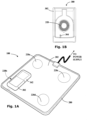
- the transmission system 100 includes an inductive power outlet 200 and an inductive power receiver 300.
- the inductive power outlet 200 is configured to transmit power to the inductive power receiver 300 wirelessly using electromagnetic induction.
- the inductive power outlet 200 of the example which is presented for illustrative purposes only, consists of four primary inductors 220a-d incorporated within a platform 202.
- the inductive power receiver 300 includes a secondary inductor 320 incorporated within a case 302 for accommodating a mobile telephone 342.
- a power connector 304 electrically connects the secondary inductor 320 with the mobile telephone 342.
- the inductive power receiver 300 may be placed upon the platform 202 in alignment with one of the primary inductors 220b so that the secondary inductor 320 inductively couples with the primary inductor 220b.
- inductive power receivers 200 may be otherwise configured, for example being incorporated within powerpacks for charging power cells or being wired directly to electrical loads 340 for powering such loads directly.
- dedicated inductive power adaptors are provided for connecting to electrical devices by power cables which may be hard wired to the adaptor or connectable via a conductive pin- and-socket connector.
- Figs. 1C, 1D and 1E show three alternative power adaptors 1300a-c according to embodiments of the inductive power receiver 300.
- Fig. 1C shows a first inductive power adaptor 1300a connected to a computer 1340a via a hardwired power cable 1310a. The first inductive power adaptor 1300a draws power from an inductive power transmitter 200 via a secondary inductor 1320.
- Fig. 1D shows a second inductive power adaptor 1300b hardwired to a light fitting 1310b for inductively powering a light bulb 1340b.
- Fig. IE shows still a third inductive power adaptor 1300c in which a conventional mains-type power socket 1310c is providing for connecting to external electrical device (not shown) via conventional power plugs.
- inductive power receivers may be used to provide power to a variety of electrical devices either via adaptors or through the inductive receiver directly into the electrical devices.
- inductive receivers may be used to power entertainment equipment such as media players, portable music players, video recorders, DVD players, portable DVD players, radios, cassette players, Walkman ® s, CD players, televisions, video players, music centers and the like.
- inductive receivers may be used in the work environment to power office equipment such as computers, telephones, PDAs, dictaphones, mobile communications devices, standing lamps, paper shredders, fans, photocopiers, printers, desk lamps, wireless telephones, mobile telephones, speakers, speaker phones, conference call base units, electric pencil sharpeners, electric staplers, display devices, electronic picture frames, VDUs, projectors, calculators, scanners, fax machines as well as heavy machinery and the like.
- office equipment such as computers, telephones, PDAs, dictaphones, mobile communications devices, standing lamps, paper shredders, fans, photocopiers, printers, desk lamps, wireless telephones, mobile telephones, speakers, speaker phones, conference call base units, electric pencil sharpeners, electric staplers, display devices, electronic picture frames, VDUs, projectors, calculators, scanners, fax machines as well as heavy machinery and the like.
- inductive power receivers may be used to provide power to devices used in the kitchen such as the cooking appliances, fridges, freezers, washing machines, clothes dryers, ambient lighting units, fans, hot plates, electrically heated mugs, egg beaters, bread-makers, liquidizers, citrus juice extractors, vegetable juicers, food-processors, electric knives, toasters, sandwich toasters, waffle makers, electrical barbecue grills, slow cookers, hot-plates, deep-fat fryers, electrical frying pans, knife sharpeners, domestic sterilizers, kettles, urns, and electrical tin-openers, popcorn makers and magnetic stirrers and the like.
- devices used in the kitchen such as the cooking appliances, fridges, freezers, washing machines, clothes dryers, ambient lighting units, fans, hot plates, electrically heated mugs, egg beaters, bread-makers, liquidizers, citrus juice extractors, vegetable juicers, food-processors, electric knives, toasters, sandwich toasters, waffle makers, electrical barbecue grills, slow cookers, hot-
- Inductive power receivers are similarly suitable for providing power to devices commonly used in the bathroom environment such as hairdryers, shavers, defoliators, delapidators, heaters, wax-melting equipment, hair curlers, beard trippers, bathroom- scales, lights and radios and such like.
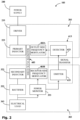
- FIG. 2 a possible configuration is represented for selected components of the inductive power transmission system 103, incorporating various frequency modulation units 403 for regulating power provided to an electrical load.
- the inductive power transmission system 103 includes an inductive power outlet 203 and an inductive power receiver 303.
- the inductive power outlet 203 includes a primary inductor 223, wired to a power source 240via a driver 233. It is noted that the inductive power outlet 203 may draw power from a variety of power sources 240, as will occur to those in the art, such as mains power points, power supply transformers, power packs, electrochemical cells, solar cells, fuel cells and the like.
- the driver 233 typically includes electronic components, such as a switching unit for example, for providing an oscillating electrical potential to the primary inductor 223. The oscillating electrical potential across the primary inductor 223 produces an oscillating magnetic field in its vicinity.
- the inductive power receiver 303 includes a secondary inductor 323 wired to an electric load 343 , typically via a rectifier 333 , a power monitor 353 and a receiver side frequency modulator 403.
- the secondary inductor 323 is configured such that, when placed in the oscillating magnetic field of an active primary inductor 223, a secondary voltage is induced across the secondary inductor 323.
- a magnetic flux guide 603 may be provided to improve inductive coupling between the primary inductor 223 and the secondary inductor 323.
- the secondary voltage may be used to power the electric load 343. It is noted that an induced secondary voltage across the secondary inductor 323 produces an alternating current (AC).
- the rectifier 333 may be provided to convert AC to DC.
- AC output is required, such as in the inductive power adaptor 1300c (Fig. IE) used for providing a mains-type output, an AC- AC converter (not shown) may be further provided.
- the receiver side frequency modulator 403B is operable to adjust the natural frequency of the inductive power transmission system 103.
- the frequency modulator 403B may variously effect the natural frequency by altering the dimensions of the secondary inductor 323, altering the permeability of the magnetic flux guide 603, changing the inductance or capacitance of the reception circuit or otherwise adjusting resonant frequency of the inductive system.
- Various examples of frequency modulators are described herein which may be used as receiver side frequency modulators 403B in such an inductive power transfer system 103.
- the power monitor 353 and receiver side frequency modulator 403 may be used in combination to regulate the power delivered to the electric load 343.
- the power monitor 353 is configured to directly monitor the output voltage produced by the secondary inductor 323 and to compare the monitored output value with the operating voltage required by the electric load 343.
- the receiver side frequency modulator 403B may be operable to bring the monitored output voltage closer to the required operating voltage of the electric load 343 by adjusting the natural frequency of the inductive transmission system 103.
- the monitor may be further configured to monitor additional operating parameters, such as temperature, current and the like.
- the inductive power transmission system 103 includes a signal transfer system 613 providing a communication channel between the inductive power outlet 203 and the inductive power receiver 303. It is noted that the inductive outlet 203 further includes an outlet side frequency modulator unit 403A, for adjusting the natural frequency of the inductive power transmission system 103,and a signal detector 623.
- the inductive power receiver 303 further includes a signal emitter 633 for sending signals to the signal detector 623.
- the power monitor 353, the signal transfer system 613 and outlet side frequency modulator 403A may be used in combination to regulate the power delivered to the electric load 343.
- the power monitor 353 is configured to directly monitor the output voltage produced by the secondary inductor 323 and to compare the monitored output value with the operating voltage required by the electric load 343.
- the signal transfer system 613 may be used to communicate signals between the inductive power receiver 303 and the inductive power outlet 203 pertaining to power regulation. Accordingly, the outlet side frequency modulator 403A may be operable to bring the monitored output voltage closer to the required operating voltage of the electric load 343 by adjusting the natural frequency of the inductive transmission system 103. Where appropriate, the signal transfer system 613 may communicate instruction signals to the inductive power outlet such as described, for example, in US 8981598 B2 .
- various signal transfer systems 613 may be used such as combinations of optical, inductive, ultrasonic signal emitters or the like and their associated detectors as well as coil-to-coil signal transmission systems. It is particularly noted that although a separate emitter 633 and secondary inductor 323 are indicated in the block diagram, the secondary inductor 323 may itself serve as a signal emitter. Similarly, although a separate detector 623 and primary inductor 223 are indicated in the block diagram, the primary inductor 223 may itself serve as a signal detector. Such a coil-to-coil signal transmission system is described for example in US 2010/0072825 A1 .
- the signal transfer system may additionally be used to communicate other signals for a variety of functions such as inter alia, confirming the presence of a power receiver 303, communicating an identification signal or for communicating required power transmission parameters. The latter being particularly useful in systems adapted to work at multiple power levels.
- the inductive outlet 203 includes an outlet side frequency modulator unit 403A and the inductive receiver 303 includes an outlet side frequency modulator unit 403B for adjusting the natural frequency of the inductive power transmission system 103.
- the power monitor 353, the signal transfer system 613, the outlet side frequency modulator 403 A, and the receiver side frequency modulator 403B may be used in combination to regulate the power delivered to the electric load 343.
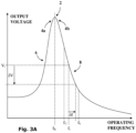
- the graph demonstrates the profile of output voltage induced in a secondary inductor over a range of transmission frequencies for an LC circuit having a fixed natural frequency f R .
- the profile demonstrates how the output voltage may be altered by adjusting transmission frequency ft of input voltage across a primary inductor.
- the strength of an induced voltage in the secondary inductor of an inductive couple varies according to the oscillating frequency of the electrical potential provided to the primary inductor.
- the induced voltage is strongest when the oscillating frequency equals the resonant frequency of the system.
- the amplitude of the voltage is at its highest when the transmission frequency is equal to the resonant frequency f R of the system, this maximum amplitude is known as the resonance peak 2. It is further noted that the slope of the graph is steepest in the regions 4a, 4b to either side of the resonance peak 2.
- inductive transfer systems which operate at or around resonance, a small variation in frequency results in a large change in induced voltage.
- a small change in the resonant frequency of the system results in a large change in the induced voltage.
- resonant inductive transfer systems may be very sensitive to small fluctuations in environmental conditions or variations in alignment between the induction coils.
- the transmission frequency may be used to regulate the inductive power transfer.
- the transmission frequency may be selected to lie within one of the near-linear regions 6, 8 where the slope of the frequency-amplitude graph is less steep.
- the frequency of transmission ft may be selected to be in the approximately linear region 8 of the curve between a lower frequency value of f L and an upper frequency value of f U
- the transmission frequency ft higher than the resonant frequency f R of the system, produces an induced voltage of Vt.
- the induced voltage may be increased by reducing the transmission frequency and the induced voltage may be reduced by increasing the transmission frequency.
- an increase in transmission frequency of ⁇ f produces a decrease in induced voltage of ⁇ V.
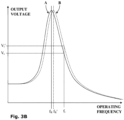
- induced power may be regulated by adjusting the natural frequency of the LC circuit for a fixed transmission frequency.
- the shift in output voltage profile of an LC circuit is illustrated when the natural frequency of the system is altered from a lower value f R to a higher value f R '.
- the output voltage peaks when the operating frequency is equal to the natural frequency f R , f R ' of the system.
- the full line A represents the voltage profile for the reception circuit with no resonance-altering component connected.
- the dashed line B represents the voltage profile for the reception circuit with a resonance-altering component connected such that the resonant frequency of the system increases from f R to f R '.
- Such an increase may be effected, for example, by using a frequency modulator such as described herein above in reference to Fig. 2 .
- the output voltage Vt may be increased by increasing the resonant frequency of the system.
- a frequency modulator increases the natural frequency of the system, an output voltage at a certain value Vt may rise to a higher value Vt'.
- a frequency modulator decreases the natural frequency of the system, the voltage profile may be shifted down and the output voltage may decrease.
- a power regulator may therefore use a frequency modulator to regulate induced power.
- the embodiments described in relation to Fig. 3B relate to inductive power transmission systems which operate at a transmission frequency f R higher than the resonant frequency ft of the system. It will be appreciated that other embodiments may operate at transmission frequencies lower than the resonant frequency ft of the system. Where the operating frequency is lower than the resonant frequency f R , the regulator may be configured to introduce resonance reducing elements into the reception circuit in order to increase the output voltage and introduce resonance increasing elements into the reception circuit in order to reduce the output voltage.
- the flowchart of Fig. 4 represents a possible method for regulating inductive power transfer using a frequency modulator.
- the method includes: driving a primary inductor at a transmission frequency significantly different from a first resonant frequency of the inductive power transfer system - step (a), inducing a secondary voltage across a secondary inductor associated with the reception circuit - step (b), monitoring the output voltage from the reception circuit - step (c).
- the monitored power may be compared to a required range - step (d). For example, a power monitor may compare the power delivered to the electric load to predetermined reference values or to reference values calculated on the fly according to varying requirements of the load. If the power lies within a required range then the natural frequency is not adjusted and the monitor continues to monitor the output voltage. If the power does not lie within the required range the frequency modulator may be used to adjust the natural frequency of the LC circuit as required.
- a first resonance-altering component to the reception circuit may be introduced such that the resonant frequency of the inductive power transfer system shifts closer to the transmission frequency
- a second resonance-altering component may be introduced such that the resonant frequency of the inductive power transfer system shifts away from the transmission frequency.
- the frequency modulator may disconnect the secondary inductor from the reception circuit as required.
- various frequency modulation units 403 may be incorporated into the system in order to adjust the natural frequency, discretely or continuously, in order to regulate the power provided to the electric load 343.
- frequency modulation units 403 may be incorporated into the system in order to adjust the natural frequency, discretely or continuously, in order to regulate the power provided to the electric load 343.
- FIGS. 5A and 5B schematic representations are presented of embodiments of inductive transfer systems which include frequency modulation coils 1420 A, 1420B operable to modify the magnetic permeability of the magnetic flux guide between the primary and secondary inductors.
- an inductive transfer system 1100A including a receiver side frequency modulator 1400 A.
- the inductive transfer system 1100A includes an inductive outlet 1200A and an inductive receiver 1300A.
- the inductive outlet 1200A comprises a driver 1230A operable to produce an alternating current potential across a primary inductor 1220A.
- the primary inductor 1220 A may be wound around a first ferromagnetic core 1620A which forms a primary side flux guide for shaping the magnetic field produced by the primary inductor and directing the flux lines towards the secondary inductor 1320A of the inductive receiver 1300 A.
- the inductive receiver 1300A comprises a secondary inductor 1320 A, a second ferromagnetic core 1630 A, a receiving circuit 1330 A, an electric load 1340A, a power monitor 1352A and a receiver side frequency modulator 1400A.
- the secondary inductor 1320 A may be wound around the second ferromagnetic core 1630 A which forms a secondary flux guide directing magnetic flux from the primary inductor 1220A therethrough.
- the electric load 1340A is wired to the secondary inductor 1320A and is operable to draw power therefrom via the receiving circuit 1330 A, which may include inter alia a rectifier unit, smoothing capacitors and such like.
- the power monitor 1352A is operable to monitor power received by the electric load 1340A and to control the receiver side frequency modulator 1400A to regulate power delivered to the electric load 1340 A by adjusting the permeability of the secondary ferromagnetic core 1630A.
- the inductance of the coupled system depends upon the inductance of the primary inductor and the inductance of the secondary inductor.
- the inductance of a solenoid, such as the primary inductor or secondary inductor depends upon the relative permeability of the magnetic core.
- the receiver side frequency modulator 1400A is operable to adjust the natural frequency of the coupled system by altering the permeability of the secondary flux guide 1630A.
- the receiver side frequency modulator 1400A includes a receiver side frequency modulation coil 1420A and a variable DC power supply 1440A.
- the receiver side frequency modulation coil 1420 A is wound around the secondary flux guide 1630A and wired to the variable DC power supply 1440A. It is noted that by applying a DC potential across the receiver side frequency modulation coil 1420A, the effective permeability of the flux guide may be altered. This may occur at least in part because the flux guide may become magnetically saturated thereby.
- the DC potential may be adjusted in response to input from the power monitor such that the natural frequency of the system may be altered.
- the power provided to the electric load may therefore be regulated by thus altering the natural frequency of the coupled system.
- a continuous variable DC supply may be used together with the frequency modulation coil 1420A to provide continuous modulation of the natural frequency over an operating range.
- the frequency modulation coil 1420A may provide discrete modulation where this may suit requirements.
- the inductive transfer system 1100B includes an inductive outlet 1200B and an inductive receiver 1300B.
- the inductive outlet 1200B comprises a driver 1230B operable to produce an alternating current potential across a primary inductor 1220B and an outlet side frequency modulator 1400B operable to modulate the natural frequency of the coupled system.
- the primary inductor 1220B may be wound around a first ferromagnetic core 1620B which forms a primary side flux guide for shaping the magnetic field produced by the primary inductor and directing the flux lines towards the secondary inductor 1320B of the inductive receiver 1300B.
- the inductive receiver 1300B comprises a secondary inductor 1320B, a second ferromagnetic core 1630B, a receiving circuit 1330B, an electric load 1340B, a power monitor 1352B.
- the secondary inductor 1320B may be wound around the second ferromagnetic core 1630B which forms a secondary flux guide directing magnetic flux from the primary inductor 1220B therethrough.
- the electric load 1340B is wired to the secondary inductor 1320B and is operable to draw power therefrom via the receiving circuit 1330B, which may include inter alia a rectifier unit, smoothing capacitors and such like.
- the power monitor 1352B is operable to monitor power received by the electric load 1340B and to communicate with the outlet side frequency modulator 1400B, for example via a communication channel such as a signal transfer system 613 ( Fig. 2 ) or the like, in order to regulate power delivered to the electric load 1340B by adjusting the permeability of the primary ferromagnetic core 1620B.
- outlet side frequency modulator 1400B is operable to adjust the natural frequency of the coupled system by altering the permeability of the secondary flux guide 1620B.
- the outlet side frequency modulator 1400B may include an outlet side frequency modulation coil 1420B and a variable DC power supply 1440B.
- the outlet side frequency modulation coil 1420B may be wound around the primary flux guide 1620B and wired to the variable DC power supply 1440B. It is noted that by applying a DC potential across the receiver side frequency modulation coil 1420B, the effective permeability of the flux guide may be altered. Accordingly, the DC potential may be adjusted in response to input from the power monitor such that the natural frequency of the system may be altered. As described herein, the power provided to the electric load may therefore be regulated by thus altering the natural frequency of the coupled system.
- frequency modulators may be operable to effect the natural frequency by altering the configuration or dimensions of elements, such as inductors or capacitors of the LC circuit of the coupled system. Accordingly, a configuration modifier may be introduced, for example, to adjust the distance between the primary and secondary inductors.
- the primary inductor may be mounted upon a travelling platform operable to shift the primary inductor radially, longitudinally or laterally relative to the secondary inductor.
- a dimension modifier may be introduced to alter the dimensions of the inductors, capacitors or their configuration in the system.
- Various dimension modifiers may be used as suit requirements, for example, a dimension modifier may be any element operable to adjust the dimensions of the system in response to electrical signals such as motors, actuators, piezoelectric element, electric field generators, bimetallic strips or the like.
- such dimension adjustments may be effected using a piezoelectric crystal configured to change shape depending upon a potential difference applied thereacross.
- Figs 6A-C illustrate such a piezoelectric crystal element 460A-C in a variety of configurations. Piezoelectric crystal elements such as this may be used as dimension modifiers in various frequency modulators.
- Figs 6A-C show the piezoelectric element 460A wired to a variable DC supply 440.
- the dimensions of the piezoelectric element 460A change as the variable DC supply 440 applies different voltages thereacross.
- the crystal may have a first width and thickness when a first voltage V 1 is applied thereacross.
- the width may be reduced and thickness increased by applying a second voltage V 2 thereacross.
- the width may be increased and thickness decreased by applying a third voltage V 3 thereacross.
- variable inductor 2220A-C is illustrated incorporating a dimension modifier 2460A-C such as a piezoelectric element or the like.
- a variable inductor 2220A-C may be incorporated into a frequency modulator such as described herein and used to modulate the natural frequency of the system so as to regulate power transfer to an electric load as described hereinabove.
- the variable inductor 2220A-C includes an inductive coil 2222A-C and a flux guide 2620, such as a ferromagnetic core or the like.
- the inductive coil 2222A-C may be coupled to the dimension modifier 2460A-C such that as the dimensions of the dimension modifier 2460A-C are adjusted, the inductive coil 2222A-C moves relative to the flux guide 2620, thereby altering the inductance of the variable inductor 2220A-C.
- a first variable capacitor 3480 is illustrated incorporating a dimension modifier 3460 such as a piezoelectric element or the like.
- a variable capacitor 3480 may be incorporated into a frequency modulator such as described herein and used to modulate the natural frequency of the system so as to regulate power transfer to an electric load as described hereinabove.
- the variable capacitor 3480 includes two electrode plates 3482A, 3482B separated by a dielectric layer 3484 and a dimension modifier 3460.
- the dimension modifier 3460 may be used to control the separation distance d between the electrode plates and may be adjusted as required.
- the dimension modifier 3460 may be introduced into the gap between the electrode plates 3482A, 3482B, for example where the dielectric layer 3484 itself comprises a dimension modifying material.
- a second variable capacitor 3480' is illustrated incorporating a dimension modifier 3460' as shown in Fig. 8B .
- the dimension modifier 3460' of the second variable capacitor 3480' is positioned outside the electrode plates and coupled thereto so as to adjust the separation distance d as required.
- a third variable capacitor 4480 is represented incorporating a dimension modifier 4460 such as a piezoelectric element or the like.
- the third variable capacitor 4480 may be incorporated into a frequency modulator such as described herein and used to modulate the natural frequency of the system so as to regulate power transfer to an electric load as described hereinabove.
- the third variable capacitor 4480 includes two electrode plates 4482A, 4482B separated by a dielectric layer 4484 and a dimension modifier 4460.
- the dimension modifier 4460 may be coupled to one of the electrode plates 4482B such that it may be shifted laterally relative to the other plate 4482A thereby controlling the overlapping area A of the electrode plates. Accordingly, the capacitance of variable capacitor may be adjusted as required.
Landscapes
- Engineering & Computer Science (AREA)
- Power Engineering (AREA)
- Computer Networks & Wireless Communication (AREA)
- Charge And Discharge Circuits For Batteries Or The Like (AREA)
- Near-Field Transmission Systems (AREA)
- Ac-Ac Conversion (AREA)
Description
- The present invention relates to regulation of power in contactless power transmission systems. More specifically, the invention relates to an inductive power transfer system as defined by the preamble portions of
claim - Inductive power transmission systems are a convenient power provision alternative to common plug and socket power connections. Inductive power transmission allows power to be transferred from an inductive power outlet to an inductive power receiver with no connecting wires.
- An oscillating electrical potential, or driving voltage, is applied across a primary inductor associated with the inductive power outlet. This produces a varying magnetic field in the vicinity of the primary inductor. When the inductive receiver is brought near to the inductive outlet, a secondary potential difference, or output voltage, is generated across a secondary inductor positioned within this varying magnetic field. The output voltage may be used to charge or power electrical devices wired to the secondary inductor.
- Systems for regulating inductive power transmission may utilize regulating mechanisms associated with the inductive power receiver or associated with the inductive power outlet.
- An inductive power transfer system as defined by the preamble portions of
claims WO2011/036659A2 and fromUS2010/0066176 A1 . - In order to maintain a stable operating voltage for an electrical device it is necessary to regulate the output voltage from the secondary inductor. Regulation of the output voltage may be provided by monitoring the output voltage, providing feedback signals from the receiver to the outlet and controlling the driving voltage accordingly.
- There is a need for a regulation system which may provide continuous regulation of power over an operating range. The disclosure herein addresses this need.
- This technical problem is solved by inductive power transfer systems as defined by
claims - For a better understanding of the invention and to show how it may be carried into effect, reference will now be made, purely by way of example, to the accompanying drawings.
- With specific reference now to the drawings in detail, it is stressed that the particulars shown are by way of example and for purposes of illustrative discussion only, and are presented in the cause of providing what is believed to be the most useful and readily understood description of the principles and conceptual aspects of the embodiments. In this regard, no attempt is made to show structural details of the embodiments in more detail than is necessary for a fundamental understanding; the description taken with the drawings making apparent to those skilled in the art how the several forms of the invention may be embodied in practice. In the accompanying drawings:
-
Figs. 1A and IB schematically represent an inductive power transmission system including an inductive power outlet and an inductive power receiver; -
Figs. 1C-E illustrate three possible inductive power adaptors for use as inductive power receivers in an inductive power transmission system; -
Figs. 2 is a block diagram showing a possible configuration of selected components of inductive power transmission systems incorporating frequency modulation units for regulating power provided to an electrical load; -
Fig. 3A is a graph showing the profile of output voltage induced in a secondary inductor over a range of transmission frequencies for an LC circuit having a fixed natural frequency and how the output voltage may be altered by adjusting transmission frequency of input voltage across a primary inductor; -
Fig. 3B is a graph showing the output voltage profile of an LC circuit for a fixed transmission frequency may be altered by adjusting natural frequency of the circuit and how the output voltage may be altered accordingly; -
Fig. 4 is a flowchart of a method for regulating inductive power transfer using a receiver based regulator; -
Figs. 5A and 5b schematically represent inductive transfer systems including possible frequency modulation coils operable to modify the magnetic permeability of the magnetic flux guide; -
Figs 6A-C schematically represent a piezoelectric crystal element which may be used as a dimension modifier in various frequency modulators of the disclosure; -
Fig. 7A-C schematically represents a frequency modulator incorporating a spacer configured to shift an inductive coil along the axis of a magnetic core so as to adjust the natural frequency of an inductive circuit; -
Figs. 8A and 8B schematically represent two possible frequency modulators incorporating a dimension modifier configured to shift parallel plates of capacitors so as to adjust the natural frequency of an LC circuit; and -
Fig 9 represents a third variable capacitor. - Reference is now made to
Figs. 1A and 1B showing an inductivepower transmission system 100. Thetransmission system 100 includes aninductive power outlet 200 and aninductive power receiver 300. Theinductive power outlet 200 is configured to transmit power to theinductive power receiver 300 wirelessly using electromagnetic induction. - The
inductive power outlet 200 of the example, which is presented for illustrative purposes only, consists of fourprimary inductors 220a-d incorporated within aplatform 202. Theinductive power receiver 300 includes asecondary inductor 320 incorporated within acase 302 for accommodating amobile telephone 342. When amobile telephone 342 is placed within the case 302 apower connector 304 electrically connects thesecondary inductor 320 with themobile telephone 342. As shown inFig. 1A , theinductive power receiver 300 may be placed upon theplatform 202 in alignment with one of theprimary inductors 220b so that thesecondary inductor 320 inductively couples with theprimary inductor 220b. - It is noted that in alternative embodiments,
inductive power receivers 200 may be otherwise configured, for example being incorporated within powerpacks for charging power cells or being wired directly to electrical loads 340 for powering such loads directly. In still other embodiments of the inductive power receiver, dedicated inductive power adaptors are provided for connecting to electrical devices by power cables which may be hard wired to the adaptor or connectable via a conductive pin- and-socket connector. -
Figs. 1C, 1D and 1E show threealternative power adaptors 1300a-c according to embodiments of theinductive power receiver 300.Fig. 1C shows a firstinductive power adaptor 1300a connected to acomputer 1340a via ahardwired power cable 1310a. The firstinductive power adaptor 1300a draws power from aninductive power transmitter 200 via asecondary inductor 1320.Fig. 1D shows a secondinductive power adaptor 1300b hardwired to alight fitting 1310b for inductively powering alight bulb 1340b. Fig. IE, shows still a thirdinductive power adaptor 1300c in which a conventional mains-type power socket 1310c is providing for connecting to external electrical device (not shown) via conventional power plugs. - It will be appreciated that various embodiments of the inductive power receiver may be used to provide power to a variety of electrical devices either via adaptors or through the inductive receiver directly into the electrical devices. Thus, for example, inductive receivers may be used to power entertainment equipment such as media players, portable music players, video recorders, DVD players, portable DVD players, radios, cassette players, Walkman®s, CD players, televisions, video players, music centers and the like.
- In addition, inductive receivers may be used in the work environment to power office equipment such as computers, telephones, PDAs, dictaphones, mobile communications devices, standing lamps, paper shredders, fans, photocopiers, printers, desk lamps, wireless telephones, mobile telephones, speakers, speaker phones, conference call base units, electric pencil sharpeners, electric staplers, display devices, electronic picture frames, VDUs, projectors, calculators, scanners, fax machines as well as heavy machinery and the like.
- Because no conductive connections are required, inductive power transfer is particularly suited for use in wet environments. Thus in some embodiments, inductive power receivers may be used to provide power to devices used in the kitchen such as the cooking appliances, fridges, freezers, washing machines, clothes dryers, ambient lighting units, fans, hot plates, electrically heated mugs, egg beaters, bread-makers, liquidizers, citrus juice extractors, vegetable juicers, food-processors, electric knives, toasters, sandwich toasters, waffle makers, electrical barbecue grills, slow cookers, hot-plates, deep-fat fryers, electrical frying pans, knife sharpeners, domestic sterilizers, kettles, urns, and electrical tin-openers, popcorn makers and magnetic stirrers and the like.
- Inductive power receivers are similarly suitable for providing power to devices commonly used in the bathroom environment such as hairdryers, shavers, defoliators, delapidators, heaters, wax-melting equipment, hair curlers, beard trippers, bathroom- scales, lights and radios and such like.
- Referring now to the block diagrams of
Figs. 2 a possible configuration is represented for selected components of the inductivepower transmission system 103, incorporating various frequency modulation units 403 for regulating power provided to an electrical load. - The inductive
power transmission system 103 includes aninductive power outlet 203 and aninductive power receiver 303. Theinductive power outlet 203 includes aprimary inductor 223, wired to a power source 240via adriver 233. It is noted that theinductive power outlet 203 may draw power from a variety ofpower sources 240, as will occur to those in the art, such as mains power points, power supply transformers, power packs, electrochemical cells, solar cells, fuel cells and the like. Thedriver 233 typically includes electronic components, such as a switching unit for example, for providing an oscillating electrical potential to theprimary inductor 223. The oscillating electrical potential across theprimary inductor 223 produces an oscillating magnetic field in its vicinity. - The
inductive power receiver 303 includes asecondary inductor 323 wired to anelectric load 343 , typically via arectifier 333 , apower monitor 353 and a receiver side frequency modulator 403. Thesecondary inductor 323 is configured such that, when placed in the oscillating magnetic field of an activeprimary inductor 223, a secondary voltage is induced across thesecondary inductor 323. Optionally amagnetic flux guide 603 may be provided to improve inductive coupling between theprimary inductor 223 and thesecondary inductor 323. The secondary voltage may be used to power theelectric load 343. It is noted that an induced secondary voltage across thesecondary inductor 323 produces an alternating current (AC). Where theelectric load 343 requires direct current (DC), such as for charging electrochemical cells, therectifier 333 may be provided to convert AC to DC. Where AC output is required, such as in theinductive power adaptor 1300c (Fig. IE) used for providing a mains-type output, an AC- AC converter (not shown) may be further provided. - The receiver
side frequency modulator 403B is operable to adjust the natural frequency of the inductivepower transmission system 103. For example, thefrequency modulator 403B may variously effect the natural frequency by altering the dimensions of thesecondary inductor 323, altering the permeability of themagnetic flux guide 603, changing the inductance or capacitance of the reception circuit or otherwise adjusting resonant frequency of the inductive system. Various examples of frequency modulators are described herein which may be used as receiverside frequency modulators 403B in such an inductivepower transfer system 103. - The
power monitor 353 and receiver side frequency modulator 403 may be used in combination to regulate the power delivered to theelectric load 343. Thepower monitor 353 is configured to directly monitor the output voltage produced by thesecondary inductor 323 and to compare the monitored output value with the operating voltage required by theelectric load 343. The receiverside frequency modulator 403B may be operable to bring the monitored output voltage closer to the required operating voltage of theelectric load 343 by adjusting the natural frequency of theinductive transmission system 103. Optionally the monitor may be further configured to monitor additional operating parameters, such as temperature, current and the like. - The inductive
power transmission system 103 includes asignal transfer system 613 providing a communication channel between theinductive power outlet 203 and theinductive power receiver 303. It is noted that theinductive outlet 203 further includes an outlet sidefrequency modulator unit 403A, for adjusting the natural frequency of the inductivepower transmission system 103,and asignal detector 623. - The
inductive power receiver 303 further includes asignal emitter 633 for sending signals to thesignal detector 623. - The
power monitor 353, thesignal transfer system 613 and outletside frequency modulator 403A may be used in combination to regulate the power delivered to theelectric load 343. Thepower monitor 353 is configured to directly monitor the output voltage produced by thesecondary inductor 323 and to compare the monitored output value with the operating voltage required by theelectric load 343. Thesignal transfer system 613 may be used to communicate signals between theinductive power receiver 303 and theinductive power outlet 203 pertaining to power regulation. Accordingly, the outletside frequency modulator 403A may be operable to bring the monitored output voltage closer to the required operating voltage of theelectric load 343 by adjusting the natural frequency of theinductive transmission system 103. Where appropriate, thesignal transfer system 613 may communicate instruction signals to the inductive power outlet such as described, for example, inUS 8981598 B2 . - It is noted that various
signal transfer systems 613 may be used such as combinations of optical, inductive, ultrasonic signal emitters or the like and their associated detectors as well as coil-to-coil signal transmission systems. It is particularly noted that although aseparate emitter 633 andsecondary inductor 323 are indicated in the block diagram, thesecondary inductor 323 may itself serve as a signal emitter. Similarly, although aseparate detector 623 andprimary inductor 223 are indicated in the block diagram, theprimary inductor 223 may itself serve as a signal detector. Such a coil-to-coil signal transmission system is described for example inUS 2010/0072825 A1 . - Furthermore, the signal transfer system may additionally be used to communicate other signals for a variety of functions such as inter alia, confirming the presence of a
power receiver 303, communicating an identification signal or for communicating required power transmission parameters. The latter being particularly useful in systems adapted to work at multiple power levels. - It is particularly noted that the
inductive outlet 203 includes an outlet sidefrequency modulator unit 403A and theinductive receiver 303 includes an outlet sidefrequency modulator unit 403B for adjusting the natural frequency of the inductivepower transmission system 103. Accordingly, thepower monitor 353, thesignal transfer system 613, the outletside frequency modulator 403 A, and the receiverside frequency modulator 403B may be used in combination to regulate the power delivered to theelectric load 343. - Reference is now made to the graph of
Fig. 3A . The graph demonstrates the profile of output voltage induced in a secondary inductor over a range of transmission frequencies for an LC circuit having a fixed natural frequency fR. The profile demonstrates how the output voltage may be altered by adjusting transmission frequency ft of input voltage across a primary inductor. - The strength of an induced voltage in the secondary inductor of an inductive couple varies according to the oscillating frequency of the electrical potential provided to the primary inductor. The induced voltage is strongest when the oscillating frequency equals the resonant frequency of the system. The resonant frequency fR depends upon the inductance L and the capacitance C of the system according to the equation

- The amplitude of the voltage is at its highest when the transmission frequency is equal to the resonant frequency fR of the system, this maximum amplitude is known as the
resonance peak 2. It is further noted that the slope of the graph is steepest in theregions resonance peak 2. Thus, in inductive transfer systems, which operate at or around resonance, a small variation in frequency results in a large change in induced voltage. Similarly, a small change in the resonant frequency of the system results in a large change in the induced voltage. For this reason, resonant inductive transfer systems may be very sensitive to small fluctuations in environmental conditions or variations in alignment between the induction coils. - In non-resonant inductive transfer systems, such as described in
US 2010/0072825 A1 , the transmission frequency may be used to regulate the inductive power transfer. The transmission frequency may be selected to lie within one of the near-linear regions linear region 8 of the curve between a lower frequency value of fL and an upper frequency value of fU Accordingly, the transmission frequency ft, higher than the resonant frequency fR of the system, produces an induced voltage of Vt. The induced voltage may be increased by reducing the transmission frequency and the induced voltage may be reduced by increasing the transmission frequency. For example, an increase in transmission frequency of δf produces a decrease in induced voltage of δV. - In other non-resonant inductive transfer systems, induced power may be regulated by adjusting the natural frequency of the LC circuit for a fixed transmission frequency. Referring now to the graph of
Fig. 3B , the shift in output voltage profile of an LC circuit is illustrated when the natural frequency of the system is altered from a lower value fR to a higher value fR'. The output voltage peaks when the operating frequency is equal to the natural frequency fR, fR' of the system. The full line A represents the voltage profile for the reception circuit with no resonance-altering component connected. The dashed line B represents the voltage profile for the reception circuit with a resonance-altering component connected such that the resonant frequency of the system increases from fR to fR'. Such an increase may be effected, for example, by using a frequency modulator such as described herein above in reference toFig. 2 . - It is noted that, for a transmission frequency ft above the resonant frequency fR of the system, the output voltage Vt may be increased by increasing the resonant frequency of the system. Thus, if a frequency modulator increases the natural frequency of the system, an output voltage at a certain value Vt may rise to a higher value Vt'. Similarly, if a frequency modulator decreases the natural frequency of the system, the voltage profile may be shifted down and the output voltage may decrease. A power regulator may therefore use a frequency modulator to regulate induced power.
- The embodiments described in relation to
Fig. 3B relate to inductive power transmission systems which operate at a transmission frequency fR higher than the resonant frequency ft of the system. It will be appreciated that other embodiments may operate at transmission frequencies lower than the resonant frequency ft of the system. Where the operating frequency is lower than the resonant frequency fR, the regulator may be configured to introduce resonance reducing elements into the reception circuit in order to increase the output voltage and introduce resonance increasing elements into the reception circuit in order to reduce the output voltage. - By way of illustration, the flowchart of
Fig. 4 represents a possible method for regulating inductive power transfer using a frequency modulator. The method includes: driving a primary inductor at a transmission frequency significantly different from a first resonant frequency of the inductive power transfer system - step (a), inducing a secondary voltage across a secondary inductor associated with the reception circuit - step (b), monitoring the output voltage from the reception circuit - step (c). - The monitored power may be compared to a required range - step (d). For example, a power monitor may compare the power delivered to the electric load to predetermined reference values or to reference values calculated on the fly according to varying requirements of the load. If the power lies within a required range then the natural frequency is not adjusted and the monitor continues to monitor the output voltage. If the power does not lie within the required range the frequency modulator may be used to adjust the natural frequency of the LC circuit as required.
- For example, if the output voltage drops below a first reference value, a first resonance-altering component to the reception circuit may be introduced such that the resonant frequency of the inductive power transfer system shifts closer to the transmission frequency, whereas if the output voltage rises above a second reference value, a second resonance-altering component may be introduced such that the resonant frequency of the inductive power transfer system shifts away from the transmission frequency. Alternatively, or additionally, the frequency modulator may disconnect the secondary inductor from the reception circuit as required.
- Referring back to
Fig. 2 , it is noted that various frequency modulation units 403 may be incorporated into the system in order to adjust the natural frequency, discretely or continuously, in order to regulate the power provided to theelectric load 343. In order to better describe the disclosure and for illustrative purposes a number of embodiments of the frequency modulation units are described below. It is to be understood that other frequency modulation units may be alternatively used as suit requirements. - Referring now to
Figs. 5A and 5B , schematic representations are presented of embodiments of inductive transfer systems which includefrequency modulation coils - With particular reference to
Fig. 5A , aninductive transfer system 1100A is presented including a receiverside frequency modulator 1400 A. Theinductive transfer system 1100A includes aninductive outlet 1200A and aninductive receiver 1300A. Theinductive outlet 1200A comprises adriver 1230A operable to produce an alternating current potential across aprimary inductor 1220A. Theprimary inductor 1220 A may be wound around a firstferromagnetic core 1620A which forms a primary side flux guide for shaping the magnetic field produced by the primary inductor and directing the flux lines towards thesecondary inductor 1320A of theinductive receiver 1300 A. Theinductive receiver 1300A comprises asecondary inductor 1320 A, a secondferromagnetic core 1630 A, a receivingcircuit 1330 A, anelectric load 1340A, apower monitor 1352A and a receiverside frequency modulator 1400A. Thesecondary inductor 1320 A may be wound around the secondferromagnetic core 1630 A which forms a secondary flux guide directing magnetic flux from theprimary inductor 1220A therethrough. Theelectric load 1340A is wired to thesecondary inductor 1320A and is operable to draw power therefrom via thereceiving circuit 1330 A, which may include inter alia a rectifier unit, smoothing capacitors and such like. Thepower monitor 1352A is operable to monitor power received by theelectric load 1340A and to control the receiverside frequency modulator 1400A to regulate power delivered to theelectric load 1340 A by adjusting the permeability of the secondaryferromagnetic core 1630A. - It is noted that the inductance of the coupled system depends upon the inductance of the primary inductor and the inductance of the secondary inductor. The inductance of a solenoid, such as the primary inductor or secondary inductor depends upon the relative permeability of the magnetic core. It is noted that the receiver
side frequency modulator 1400A is operable to adjust the natural frequency of the coupled system by altering the permeability of thesecondary flux guide 1630A. - The receiver
side frequency modulator 1400A includes a receiver sidefrequency modulation coil 1420A and a variableDC power supply 1440A. The receiver sidefrequency modulation coil 1420 A is wound around thesecondary flux guide 1630A and wired to the variableDC power supply 1440A. It is noted that by applying a DC potential across the receiver sidefrequency modulation coil 1420A, the effective permeability of the flux guide may be altered. This may occur at least in part because the flux guide may become magnetically saturated thereby. - Accordingly, the DC potential may be adjusted in response to input from the power monitor such that the natural frequency of the system may be altered. As described herein, the power provided to the electric load may therefore be regulated by thus altering the natural frequency of the coupled system.
- It is particularly noted that a continuous variable DC supply may be used together with the
frequency modulation coil 1420A to provide continuous modulation of the natural frequency over an operating range. Alternatively, or additionally, thefrequency modulation coil 1420A may provide discrete modulation where this may suit requirements. - Referring now to
Fig. 5B , an alternativeinductive transfer system 1100B is presented including an outletside frequency modulator 1400B. Theinductive transfer system 1100B includes aninductive outlet 1200B and aninductive receiver 1300B. Theinductive outlet 1200B comprises adriver 1230B operable to produce an alternating current potential across aprimary inductor 1220B and an outletside frequency modulator 1400B operable to modulate the natural frequency of the coupled system. Theprimary inductor 1220B may be wound around a firstferromagnetic core 1620B which forms a primary side flux guide for shaping the magnetic field produced by the primary inductor and directing the flux lines towards thesecondary inductor 1320B of theinductive receiver 1300B. Theinductive receiver 1300B comprises asecondary inductor 1320B, a secondferromagnetic core 1630B, a receivingcircuit 1330B, anelectric load 1340B, apower monitor 1352B. Thesecondary inductor 1320B may be wound around the secondferromagnetic core 1630B which forms a secondary flux guide directing magnetic flux from theprimary inductor 1220B therethrough. Theelectric load 1340B is wired to thesecondary inductor 1320B and is operable to draw power therefrom via the receivingcircuit 1330B, which may include inter alia a rectifier unit, smoothing capacitors and such like. Thepower monitor 1352B is operable to monitor power received by theelectric load 1340B and to communicate with the outletside frequency modulator 1400B, for example via a communication channel such as a signal transfer system 613 (Fig. 2 ) or the like, in order to regulate power delivered to theelectric load 1340B by adjusting the permeability of the primaryferromagnetic core 1620B. - It is noted that the outlet
side frequency modulator 1400B is operable to adjust the natural frequency of the coupled system by altering the permeability of thesecondary flux guide 1620B. - The outlet
side frequency modulator 1400B may include an outlet sidefrequency modulation coil 1420B and a variableDC power supply 1440B. The outlet sidefrequency modulation coil 1420B may be wound around theprimary flux guide 1620B and wired to the variableDC power supply 1440B. It is noted that by applying a DC potential across the receiver sidefrequency modulation coil 1420B, the effective permeability of the flux guide may be altered. Accordingly, the DC potential may be adjusted in response to input from the power monitor such that the natural frequency of the system may be altered. As described herein, the power provided to the electric load may therefore be regulated by thus altering the natural frequency of the coupled system. - As noted above, frequency modulators may be operable to effect the natural frequency by altering the configuration or dimensions of elements, such as inductors or capacitors of the LC circuit of the coupled system. Accordingly, a configuration modifier may be introduced, for example, to adjust the distance between the primary and secondary inductors. Where appropriate the primary inductor may be mounted upon a travelling platform operable to shift the primary inductor radially, longitudinally or laterally relative to the secondary inductor.
- Additionally or alternatively, a dimension modifier may be introduced to alter the dimensions of the inductors, capacitors or their configuration in the system. Various dimension modifiers may be used as suit requirements, for example, a dimension modifier may be any element operable to adjust the dimensions of the system in response to electrical signals such as motors, actuators, piezoelectric element, electric field generators, bimetallic strips or the like.
- By way of example only, such dimension adjustments may be effected using a piezoelectric crystal configured to change shape depending upon a potential difference applied thereacross.
Figs 6A-C illustrate such apiezoelectric crystal element 460A-C in a variety of configurations. Piezoelectric crystal elements such as this may be used as dimension modifiers in various frequency modulators. -
Figs 6A-C show thepiezoelectric element 460A wired to avariable DC supply 440. The dimensions of thepiezoelectric element 460A change as thevariable DC supply 440 applies different voltages thereacross. Accordingly, as illustrated inFig. 6A , the crystal may have a first width and thickness when a first voltage V1 is applied thereacross. As shown inFig. 6B , the width may be reduced and thickness increased by applying a second voltage V2 thereacross. As shown inFig. 6C , the width may be increased and thickness decreased by applying a third voltage V3 thereacross. - Referring now to
Figs. 7A-C , avariable inductor 2220A-C is illustrated incorporating adimension modifier 2460A-C such as a piezoelectric element or the like. Such avariable inductor 2220A-C may be incorporated into a frequency modulator such as described herein and used to modulate the natural frequency of the system so as to regulate power transfer to an electric load as described hereinabove. Thevariable inductor 2220A-C includes aninductive coil 2222A-C and aflux guide 2620, such as a ferromagnetic core or the like. Theinductive coil 2222A-C may be coupled to thedimension modifier 2460A-C such that as the dimensions of thedimension modifier 2460A-C are adjusted, theinductive coil 2222A-C moves relative to theflux guide 2620, thereby altering the inductance of thevariable inductor 2220A-C. - Referring now to
Fig. 8A , a firstvariable capacitor 3480 is illustrated incorporating adimension modifier 3460 such as a piezoelectric element or the like. Such avariable capacitor 3480 may be incorporated into a frequency modulator such as described herein and used to modulate the natural frequency of the system so as to regulate power transfer to an electric load as described hereinabove. - The
variable capacitor 3480 includes twoelectrode plates dielectric layer 3484 and adimension modifier 3460. Thedimension modifier 3460 may be used to control the separation distance d between the electrode plates and may be adjusted as required. Optionally, thedimension modifier 3460 may be introduced into the gap between theelectrode plates dielectric layer 3484 itself comprises a dimension modifying material. - Referring now to
Fig. 8B , alternatively, or additionally, a second variable capacitor 3480' is illustrated incorporating a dimension modifier 3460' as shown inFig. 8B . The dimension modifier 3460' of the second variable capacitor 3480' is positioned outside the electrode plates and coupled thereto so as to adjust the separation distance d as required. - With reference to
Fig. 9 , a thirdvariable capacitor 4480 is represented incorporating adimension modifier 4460 such as a piezoelectric element or the like. The thirdvariable capacitor 4480 may be incorporated into a frequency modulator such as described herein and used to modulate the natural frequency of the system so as to regulate power transfer to an electric load as described hereinabove. - The third
variable capacitor 4480 includes twoelectrode plates dielectric layer 4484 and adimension modifier 4460. Thedimension modifier 4460 may be coupled to one of theelectrode plates 4482B such that it may be shifted laterally relative to theother plate 4482A thereby controlling the overlapping area A of the electrode plates. Accordingly, the capacitance of variable capacitor may be adjusted as required.
Claims (10)
- An inductive power transfer system (103) comprising:
an inductive power outlet (203) for providing induced power to at least one electric load (343) via at least one inductive power receiver 303), said inductive power outlet (203) comprising:at least one primary inductor (223) for forming an inductive couple with at least one secondary inductor (323) of the at least one inductive power receiver (300);a driver (233) configured to provide a driving voltage across the primary inductor (223), the driving voltage oscillating at a transmission frequency significantly different from the inductive couple natural frequency;the inductive power transfer system further comprising a signal transfer system (613) configured to communicate instruction signals to the inductive power outlet, the signal transfer system comprising a signal detector (623) operable to receive the instruction signals from a signal emitter (633) associated with the inductive power receiver (303) during power transfer; andat least one outlet-side frequency modulator (403A); andan inductive power receiver (303) for providing power to an electric load (343), said inductive power receiver (303) comprising:at least one secondary inductor (323) for forming an inductive couple with said primary inductor (223) associated with said inductive power outlet (203);at least one power monitor (353) operable to monitor output power of the secondary inductor (323); anda receiver-side frequency modulator (403B);wherein the receiver-side frequency modulator and/or the at least one outlet-side frequency modulator are capable of adjusting natural frequency of the inductive couple in order to regulate the induced power to the at least one electric load, said frequency modulator (403A, 403B) comprising at least of component selected from a group comprising of at least one variable capacitor (3480, 4480) and at least one variable inductor (2220A-C) and a combination thereofcharacterized in thatsaid adjusting the natural frequency is characterized by modifying the physical dimensions of the at least one component. - An inductive power transfer system (103) comprising:
an inductive power outlet (203) for providing induced power to at least one electric load (343) via at least one inductive power receiver (303), said inductive power outlet (203) comprising:at least one primary inductor (223) for forming an inductive couple with at least one secondary inductor (323) of the at least one inductive power receiver (300);a driver (233) configured to provide a driving voltage across the primary inductor (223), the driving voltage oscillating at a transmission frequency significantly different from the inductive couple natural frequency;the inductive power transfer system further comprising a signal transfer system (613) configured to communicate instruction signals to the inductive power outlet, the signal transfer system comprising a signal detector (623) operable to receive the instruction signals from a signal emitter (633) associated with the inductive power receiver (303) during power transfer; andat least one outlet-side frequency modulator (403A); andan inductive power receiver (303) for providing power to an electric load (343), said inductive power receiver (303) comprising:at least one secondary inductor (323) for forming an inductive couple with said primary inductor (223) associated with said inductive power outlet (203);at least one power monitor (353) operable to monitor output power of the secondary inductor (323); anda receiver-side frequency modulator (403B);wherein the receiver-side frequency modulator and/or the at least one outlet-side frequency modulator are capable of adjusting natural frequency of the inductive couple in order to regulate the induced power to the at least one electric load, said frequency modulator (403A, 403B) comprising at least one frequency modulation coil (1420A, 1420B),characterized in thatsaid adjusting the natural frequency is characterized by modifying the magnetic permeability of at least one magnetic flux guide (1620A, 1620B, 1630A, 1630B). - The inductive power transfer system of claim 1 wherein the frequency modulator (403) comprises at least one dimension modifier (2460A-C) configured to modify the dimensions of at least one inductor.
- The inductive power transfer system or the inductive power outlet of claim 3 wherein the dimension modifier (2460A-C) is configured to adjust distance between an inductive coil (2222A-C) and a ferromagnetic core (2620).
- The inductive power transfer system of claim 1 wherein the frequency modulator (403) comprises at least one dimension modifier (3460, 3460', 4460) configured to modify the dimensions of at least one capacitor (3480, 3480', 4480).
- The inductive power transfer system of claim 5 wherein the dimension modifier (3460) comprises at least one piezoelectric crystal (460) wired to a variable direct current supply (440) and coupled to at least one capacitive plate (3482A, 3482B, 4482A, 4482B) of the capacitor (3480, 4480) such that the distance between the capacitive plates is adjusted when the direct current supply is varied.
- The inductive power transfer system of claim 2 wherein said at least one magnetic flux guide (1620A, 1630A, 1620B, 1630B) is configured for directing magnetic flux from the primary inductor (1220A, 1220B) to the secondary inductor (1320A, 1320B), wherein the frequency modulator (1400A, 1400B) comprises at least one modulation coil (1420A, 1420B) wired to a variable direct current supply (1440A, 1440B) and operable to modify magnetic permeability of the magnetic flux guide (1620A, 1630A, 1630A, 1630B).
- The inductive power transfer system of claim 1 further comprising at least one magnetic flux guide (2620) for directing magnetic flux from the primary inductor (223) to the secondary inductor (323) wherein the frequency modulator (403A, 403B) comprises at least one dimension modifier (460, 2460A-C) configured to adjust the dimensions between the flux guide (2620) and at least one of the primary inductor (223) and the secondary inductor (323).
- The inductive power transfer system of claim 8 wherein the dimension modifier (460, 2460A-C) comprises at least one piezoelectric crystal (440) coupled to the flux guide (2620) and the secondary inductor (323) and wired to a variable direct current supply (440) such that the distance between the flux guide (2620) and the inductor is adjusted when the direct current supply is varied.
- The inductive transfer system outlet of claims 1 and 2, wherein the signal detector (623) comprises the primary inductor (223) operable to detect signals emitted by the secondary inductor (323) as a coil-to-coil signal transmission system.
Applications Claiming Priority (2)
| Application Number | Priority Date | Filing Date | Title |
|---|---|---|---|
| US201161566103P | 2011-12-02 | 2011-12-02 | |
| PCT/IL2012/050491 WO2013080212A2 (en) | 2011-12-02 | 2012-11-29 | System and method for regulating inductive power transmission |
Publications (3)
| Publication Number | Publication Date |
|---|---|
| EP2786464A2 EP2786464A2 (en) | 2014-10-08 |
| EP2786464B1 EP2786464B1 (en) | 2019-05-01 |
| EP2786464B2 true EP2786464B2 (en) | 2023-03-29 |
Family
ID=47633135
Family Applications (1)
| Application Number | Title | Priority Date | Filing Date |
|---|---|---|---|
| EP12821136.4A Active EP2786464B2 (en) | 2011-12-02 | 2012-11-29 | System and method for regulating inductive power transmission |
Country Status (2)
| Country | Link |
|---|---|
| EP (1) | EP2786464B2 (en) |
| WO (1) | WO2013080212A2 (en) |
Families Citing this family (6)
| Publication number | Priority date | Publication date | Assignee | Title |
|---|---|---|---|---|
| CN104854771B (en) | 2012-10-29 | 2019-07-19 | 苹果公司 | Receiver of an inductive power transfer system and method for controlling the same |
| EP3108487B1 (en) * | 2014-01-22 | 2019-02-27 | Apple Inc. | Coupled-coil power control for inductive power transfer systems |
| EP3216108A4 (en) | 2014-11-05 | 2017-10-25 | PowerbyProxi Limited | An inductive power receiver |
| WO2017131531A1 (en) * | 2016-01-26 | 2017-08-03 | Powerbyproxi Limited | Inductive power transfer |
| US10355532B2 (en) | 2016-11-02 | 2019-07-16 | Apple Inc. | Inductive power transfer |
| US10447090B1 (en) | 2016-11-17 | 2019-10-15 | Apple Inc. | Inductive power receiver |
Citations (4)
| Publication number | Priority date | Publication date | Assignee | Title |
|---|---|---|---|---|
| US20100072825A1 (en) † | 2007-03-22 | 2010-03-25 | Powermat Ltd | System and method for controlling power transfer across an inductive power coupling |
| US20100148589A1 (en) † | 2008-10-01 | 2010-06-17 | Hamam Rafif E | Efficient near-field wireless energy transfer using adiabatic system variations |
| US20100259108A1 (en) † | 2008-09-27 | 2010-10-14 | Giler Eric R | Wireless energy transfer using repeater resonators |
| US20110121658A1 (en) † | 2008-04-15 | 2011-05-26 | Toyota Jidosha Kabushiki Kaisha | Wireless energy transfer device |
Family Cites Families (5)
| Publication number | Priority date | Publication date | Assignee | Title |
|---|---|---|---|---|
| US6556415B1 (en) * | 2002-06-28 | 2003-04-29 | Industrial Technologies Research Institute | Tunable/variable passive microelectronic components |
| JP4308858B2 (en) * | 2007-02-16 | 2009-08-05 | セイコーエプソン株式会社 | Power transmission control device, power reception control device, non-contact power transmission system, power transmission device, power reception device, and electronic equipment |
| US8188619B2 (en) * | 2008-07-02 | 2012-05-29 | Powermat Technologies Ltd | Non resonant inductive power transmission system and method |
| US7858878B2 (en) | 2008-09-15 | 2010-12-28 | Honeywell International Inc. | Flush mount-corner mount gang box |
| JP2013506399A (en) | 2009-09-28 | 2013-02-21 | パワーマット テクノロジーズ リミテッド | System and method for regulating inductive power transfer |
-
2012
- 2012-11-29 EP EP12821136.4A patent/EP2786464B2/en active Active
- 2012-11-29 WO PCT/IL2012/050491 patent/WO2013080212A2/en not_active Ceased
Patent Citations (4)
| Publication number | Priority date | Publication date | Assignee | Title |
|---|---|---|---|---|
| US20100072825A1 (en) † | 2007-03-22 | 2010-03-25 | Powermat Ltd | System and method for controlling power transfer across an inductive power coupling |
| US20110121658A1 (en) † | 2008-04-15 | 2011-05-26 | Toyota Jidosha Kabushiki Kaisha | Wireless energy transfer device |
| US20100259108A1 (en) † | 2008-09-27 | 2010-10-14 | Giler Eric R | Wireless energy transfer using repeater resonators |
| US20100148589A1 (en) † | 2008-10-01 | 2010-06-17 | Hamam Rafif E | Efficient near-field wireless energy transfer using adiabatic system variations |
Also Published As
| Publication number | Publication date |
|---|---|
| EP2786464A2 (en) | 2014-10-08 |
| WO2013080212A3 (en) | 2013-07-25 |
| EP2786464B1 (en) | 2019-05-01 |
| WO2013080212A2 (en) | 2013-06-06 |
Similar Documents
| Publication | Publication Date | Title |
|---|---|---|
| US20130049482A1 (en) | System and method for regulating inductive power transmission | |
| US9960640B2 (en) | System and method for regulating inductive power transmission | |
| US9478991B2 (en) | System and method for transferring power inductively over an extended region | |
| EP2786464B2 (en) | System and method for regulating inductive power transmission | |
| CN103259344B (en) | Circuit for induced power transmission | |
| KR102579343B1 (en) | Wireless power transfer system configuration | |
| JP6084994B2 (en) | Wireless power receiving apparatus, terminal, and wireless power transmitting apparatus | |
| US10529484B2 (en) | Coil device of wireless power transfer system | |
| JP5939314B2 (en) | Electronic device and wireless power transmission system | |
| US10326315B2 (en) | Wireless power transmission apparatus | |
| EP3611821A1 (en) | Packaging and details of a wireless power device | |
| JP5674013B2 (en) | Power supply device and power supply system | |
| EP3282545A1 (en) | Wireless power transmission device and control method therefor | |
| KR20170005589A (en) | Apparatus for transmitting wireless power and system for transmitting wireless power | |
| KR20180021559A (en) | Wireless power transmitter | |
| KR20170010870A (en) | Apparatus for wireless power transmission and the control method thereof | |
| KR20160124568A (en) | Apparatus for transmitting wireless power and the control method thereof | |
| KR20160070539A (en) | Wireless Power Transfer System | |
| KR20170006394A (en) | Operating method for wireless power transmitting apparatus | |
| KR20180020796A (en) | Wireless power transmitter and thereof operation method | |
| KR20170082309A (en) | A wireless power transmitter and a wireless power receiver of wireless power transfer system |
Legal Events
| Date | Code | Title | Description |
|---|---|---|---|
| PUAI | Public reference made under article 153(3) epc to a published international application that has entered the european phase |
Free format text: ORIGINAL CODE: 0009012 |
|
| 17P | Request for examination filed |
Effective date: 20140701 |
|
| AK | Designated contracting states |
Kind code of ref document: A2 Designated state(s): AL AT BE BG CH CY CZ DE DK EE ES FI FR GB GR HR HU IE IS IT LI LT LU LV MC MK MT NL NO PL PT RO RS SE SI SK SM TR |
|
| DAX | Request for extension of the european patent (deleted) | ||
| 17Q | First examination report despatched |
Effective date: 20160509 |
|
| STAA | Information on the status of an ep patent application or granted ep patent |
Free format text: STATUS: EXAMINATION IS IN PROGRESS |
|
| RIC1 | Information provided on ipc code assigned before grant |
Ipc: H02J 50/12 20160101ALI20180928BHEP Ipc: H02J 7/02 20060101ALI20180928BHEP Ipc: H02J 50/80 20160101ALI20180928BHEP Ipc: H02J 5/00 20060101AFI20180928BHEP |
|
| GRAP | Despatch of communication of intention to grant a patent |
Free format text: ORIGINAL CODE: EPIDOSNIGR1 |
|
| STAA | Information on the status of an ep patent application or granted ep patent |
Free format text: STATUS: GRANT OF PATENT IS INTENDED |
|
| INTG | Intention to grant announced |
Effective date: 20181120 |
|
| RIC1 | Information provided on ipc code assigned before grant |
Ipc: H02J 5/00 20160101AFI20180928BHEP Ipc: H02J 50/80 20160101ALI20180928BHEP Ipc: H02J 7/02 20160101ALI20180928BHEP Ipc: H02J 50/12 20160101ALI20180928BHEP |
|
| GRAS | Grant fee paid |
Free format text: ORIGINAL CODE: EPIDOSNIGR3 |
|
| GRAA | (expected) grant |
Free format text: ORIGINAL CODE: 0009210 |
|
| STAA | Information on the status of an ep patent application or granted ep patent |
Free format text: STATUS: THE PATENT HAS BEEN GRANTED |
|
| AK | Designated contracting states |
Kind code of ref document: B1 Designated state(s): AL AT BE BG CH CY CZ DE DK EE ES FI FR GB GR HR HU IE IS IT LI LT LU LV MC MK MT NL NO PL PT RO RS SE SI SK SM TR |
|
| REG | Reference to a national code |
Ref country code: GB Ref legal event code: FG4D |
|
| REG | Reference to a national code |
Ref country code: DE Ref legal event code: R081 Ref document number: 602012059677 Country of ref document: DE Owner name: POWERMAT TECHNOLOGIES LTD., IL Free format text: FORMER OWNER: GREENWALD, OOLA, MEVASSERET ZION, IL |
|
| REG | Reference to a national code |
Ref country code: CH Ref legal event code: EP Ref country code: AT Ref legal event code: REF Ref document number: 1128202 Country of ref document: AT Kind code of ref document: T Effective date: 20190515 |
|
| REG | Reference to a national code |
Ref country code: DE Ref legal event code: R096 Ref document number: 602012059677 Country of ref document: DE |
|
| REG | Reference to a national code |
Ref country code: IE Ref legal event code: FG4D |
|
| REG | Reference to a national code |
Ref country code: DE Ref legal event code: R082 Ref document number: 602012059677 Country of ref document: DE Representative=s name: BECK & ROESSIG - EUROPEAN PATENT ATTORNEYS, DE Ref country code: DE Ref legal event code: R081 Ref document number: 602012059677 Country of ref document: DE Owner name: POWERMAT TECHNOLOGIES LTD., IL Free format text: FORMER OWNERS: GREENWALD, OOLA, MEVASSERET ZION, IL; MACH, ELIESER, ROSH TZURIM, IL; POWERMAT TECHNOLOGIES LTD., NEVE ILAN, IL; RAVEH, GUY, MATAA, IL; ROFE, ARIK, JERUSALEM, IL Ref country code: DE Ref legal event code: R082 Ref document number: 602012059677 Country of ref document: DE Representative=s name: MAIWALD PATENTANWALTS- UND RECHTSANWALTSGESELL, DE |
|
| REG | Reference to a national code |
Ref country code: GB Ref legal event code: 732E Free format text: REGISTERED BETWEEN 20190718 AND 20190724 |
|
| REG | Reference to a national code |
Ref country code: NL Ref legal event code: MP Effective date: 20190501 |
|
| RAP2 | Party data changed (patent owner data changed or rights of a patent transferred) |
Owner name: ROFE, ARIK Owner name: RAVEH, GUY Owner name: GREENWALD, OOLA Owner name: MACH, ELIESER Owner name: POWERMAT TECHNOLOGIES LTD. |
|
| REG | Reference to a national code |
Ref country code: LT Ref legal event code: MG4D |
|
| PG25 | Lapsed in a contracting state [announced via postgrant information from national office to epo] |
Ref country code: FI Free format text: LAPSE BECAUSE OF FAILURE TO SUBMIT A TRANSLATION OF THE DESCRIPTION OR TO PAY THE FEE WITHIN THE PRESCRIBED TIME-LIMIT Effective date: 20190501 Ref country code: NO Free format text: LAPSE BECAUSE OF FAILURE TO SUBMIT A TRANSLATION OF THE DESCRIPTION OR TO PAY THE FEE WITHIN THE PRESCRIBED TIME-LIMIT Effective date: 20190801 Ref country code: NL Free format text: LAPSE BECAUSE OF FAILURE TO SUBMIT A TRANSLATION OF THE DESCRIPTION OR TO PAY THE FEE WITHIN THE PRESCRIBED TIME-LIMIT Effective date: 20190501 Ref country code: AL Free format text: LAPSE BECAUSE OF FAILURE TO SUBMIT A TRANSLATION OF THE DESCRIPTION OR TO PAY THE FEE WITHIN THE PRESCRIBED TIME-LIMIT Effective date: 20190501 Ref country code: SE Free format text: LAPSE BECAUSE OF FAILURE TO SUBMIT A TRANSLATION OF THE DESCRIPTION OR TO PAY THE FEE WITHIN THE PRESCRIBED TIME-LIMIT Effective date: 20190501 Ref country code: PT Free format text: LAPSE BECAUSE OF FAILURE TO SUBMIT A TRANSLATION OF THE DESCRIPTION OR TO PAY THE FEE WITHIN THE PRESCRIBED TIME-LIMIT Effective date: 20190901 Ref country code: LT Free format text: LAPSE BECAUSE OF FAILURE TO SUBMIT A TRANSLATION OF THE DESCRIPTION OR TO PAY THE FEE WITHIN THE PRESCRIBED TIME-LIMIT Effective date: 20190501 Ref country code: HR Free format text: LAPSE BECAUSE OF FAILURE TO SUBMIT A TRANSLATION OF THE DESCRIPTION OR TO PAY THE FEE WITHIN THE PRESCRIBED TIME-LIMIT Effective date: 20190501 Ref country code: ES Free format text: LAPSE BECAUSE OF FAILURE TO SUBMIT A TRANSLATION OF THE DESCRIPTION OR TO PAY THE FEE WITHIN THE PRESCRIBED TIME-LIMIT Effective date: 20190501 |
|
| PG25 | Lapsed in a contracting state [announced via postgrant information from national office to epo] |
Ref country code: GR Free format text: LAPSE BECAUSE OF FAILURE TO SUBMIT A TRANSLATION OF THE DESCRIPTION OR TO PAY THE FEE WITHIN THE PRESCRIBED TIME-LIMIT Effective date: 20190802 Ref country code: RS Free format text: LAPSE BECAUSE OF FAILURE TO SUBMIT A TRANSLATION OF THE DESCRIPTION OR TO PAY THE FEE WITHIN THE PRESCRIBED TIME-LIMIT Effective date: 20190501 Ref country code: BG Free format text: LAPSE BECAUSE OF FAILURE TO SUBMIT A TRANSLATION OF THE DESCRIPTION OR TO PAY THE FEE WITHIN THE PRESCRIBED TIME-LIMIT Effective date: 20190801 Ref country code: LV Free format text: LAPSE BECAUSE OF FAILURE TO SUBMIT A TRANSLATION OF THE DESCRIPTION OR TO PAY THE FEE WITHIN THE PRESCRIBED TIME-LIMIT Effective date: 20190501 |
|
| REG | Reference to a national code |
Ref country code: AT Ref legal event code: MK05 Ref document number: 1128202 Country of ref document: AT Kind code of ref document: T Effective date: 20190501 |
|
| PG25 | Lapsed in a contracting state [announced via postgrant information from national office to epo] |
Ref country code: IS Free format text: LAPSE BECAUSE OF FAILURE TO SUBMIT A TRANSLATION OF THE DESCRIPTION OR TO PAY THE FEE WITHIN THE PRESCRIBED TIME-LIMIT Effective date: 20190901 |
|
| PG25 | Lapsed in a contracting state [announced via postgrant information from national office to epo] |
Ref country code: RO Free format text: LAPSE BECAUSE OF FAILURE TO SUBMIT A TRANSLATION OF THE DESCRIPTION OR TO PAY THE FEE WITHIN THE PRESCRIBED TIME-LIMIT Effective date: 20190501 Ref country code: CZ Free format text: LAPSE BECAUSE OF FAILURE TO SUBMIT A TRANSLATION OF THE DESCRIPTION OR TO PAY THE FEE WITHIN THE PRESCRIBED TIME-LIMIT Effective date: 20190501 Ref country code: EE Free format text: LAPSE BECAUSE OF FAILURE TO SUBMIT A TRANSLATION OF THE DESCRIPTION OR TO PAY THE FEE WITHIN THE PRESCRIBED TIME-LIMIT Effective date: 20190501 Ref country code: DK Free format text: LAPSE BECAUSE OF FAILURE TO SUBMIT A TRANSLATION OF THE DESCRIPTION OR TO PAY THE FEE WITHIN THE PRESCRIBED TIME-LIMIT Effective date: 20190501 Ref country code: AT Free format text: LAPSE BECAUSE OF FAILURE TO SUBMIT A TRANSLATION OF THE DESCRIPTION OR TO PAY THE FEE WITHIN THE PRESCRIBED TIME-LIMIT Effective date: 20190501 Ref country code: SK Free format text: LAPSE BECAUSE OF FAILURE TO SUBMIT A TRANSLATION OF THE DESCRIPTION OR TO PAY THE FEE WITHIN THE PRESCRIBED TIME-LIMIT Effective date: 20190501 |
|
| REG | Reference to a national code |
Ref country code: DE Ref legal event code: R026 Ref document number: 602012059677 Country of ref document: DE |
|
| PLBI | Opposition filed |
Free format text: ORIGINAL CODE: 0009260 |
|
| PLAX | Notice of opposition and request to file observation + time limit sent |
Free format text: ORIGINAL CODE: EPIDOSNOBS2 |
|
| PG25 | Lapsed in a contracting state [announced via postgrant information from national office to epo] |
Ref country code: IT Free format text: LAPSE BECAUSE OF FAILURE TO SUBMIT A TRANSLATION OF THE DESCRIPTION OR TO PAY THE FEE WITHIN THE PRESCRIBED TIME-LIMIT Effective date: 20190501 Ref country code: SM Free format text: LAPSE BECAUSE OF FAILURE TO SUBMIT A TRANSLATION OF THE DESCRIPTION OR TO PAY THE FEE WITHIN THE PRESCRIBED TIME-LIMIT Effective date: 20190501 |
|
| 26 | Opposition filed |
Opponent name: IKEA SUPPLY AG Effective date: 20200131 |
|
| PG25 | Lapsed in a contracting state [announced via postgrant information from national office to epo] |
Ref country code: TR Free format text: LAPSE BECAUSE OF FAILURE TO SUBMIT A TRANSLATION OF THE DESCRIPTION OR TO PAY THE FEE WITHIN THE PRESCRIBED TIME-LIMIT Effective date: 20190501 |
|
| PG25 | Lapsed in a contracting state [announced via postgrant information from national office to epo] |
Ref country code: PL Free format text: LAPSE BECAUSE OF FAILURE TO SUBMIT A TRANSLATION OF THE DESCRIPTION OR TO PAY THE FEE WITHIN THE PRESCRIBED TIME-LIMIT Effective date: 20190501 |
|
| PG25 | Lapsed in a contracting state [announced via postgrant information from national office to epo] |
Ref country code: SI Free format text: LAPSE BECAUSE OF FAILURE TO SUBMIT A TRANSLATION OF THE DESCRIPTION OR TO PAY THE FEE WITHIN THE PRESCRIBED TIME-LIMIT Effective date: 20190501 |
|
| REG | Reference to a national code |
Ref country code: CH Ref legal event code: PL |
|
| PG25 | Lapsed in a contracting state [announced via postgrant information from national office to epo] |
Ref country code: CH Free format text: LAPSE BECAUSE OF NON-PAYMENT OF DUE FEES Effective date: 20191130 Ref country code: LI Free format text: LAPSE BECAUSE OF NON-PAYMENT OF DUE FEES Effective date: 20191130 Ref country code: LU Free format text: LAPSE BECAUSE OF NON-PAYMENT OF DUE FEES Effective date: 20191129 Ref country code: MC Free format text: LAPSE BECAUSE OF FAILURE TO SUBMIT A TRANSLATION OF THE DESCRIPTION OR TO PAY THE FEE WITHIN THE PRESCRIBED TIME-LIMIT Effective date: 20190501 |
|
| REG | Reference to a national code |
Ref country code: BE Ref legal event code: MM Effective date: 20191130 |
|
| PLBB | Reply of patent proprietor to notice(s) of opposition received |
Free format text: ORIGINAL CODE: EPIDOSNOBS3 |
|
| PG25 | Lapsed in a contracting state [announced via postgrant information from national office to epo] |
Ref country code: IE Free format text: LAPSE BECAUSE OF NON-PAYMENT OF DUE FEES Effective date: 20191129 |
|
| PG25 | Lapsed in a contracting state [announced via postgrant information from national office to epo] |
Ref country code: BE Free format text: LAPSE BECAUSE OF NON-PAYMENT OF DUE FEES Effective date: 20191130 |
|
| REG | Reference to a national code |
Ref country code: DE Ref legal event code: R082 Ref document number: 602012059677 Country of ref document: DE Representative=s name: MAIWALD GMBH, DE Ref country code: DE Ref legal event code: R082 Ref document number: 602012059677 Country of ref document: DE Representative=s name: MAIWALD PATENTANWALTS- UND RECHTSANWALTSGESELL, DE |
|
| PG25 | Lapsed in a contracting state [announced via postgrant information from national office to epo] |
Ref country code: CY Free format text: LAPSE BECAUSE OF FAILURE TO SUBMIT A TRANSLATION OF THE DESCRIPTION OR TO PAY THE FEE WITHIN THE PRESCRIBED TIME-LIMIT Effective date: 20190501 |
|
| PG25 | Lapsed in a contracting state [announced via postgrant information from national office to epo] |
Ref country code: MT Free format text: LAPSE BECAUSE OF FAILURE TO SUBMIT A TRANSLATION OF THE DESCRIPTION OR TO PAY THE FEE WITHIN THE PRESCRIBED TIME-LIMIT Effective date: 20190501 Ref country code: HU Free format text: LAPSE BECAUSE OF FAILURE TO SUBMIT A TRANSLATION OF THE DESCRIPTION OR TO PAY THE FEE WITHIN THE PRESCRIBED TIME-LIMIT; INVALID AB INITIO Effective date: 20121129 |
|
| RIC2 | Information provided on ipc code assigned after grant |
Ipc: H02J 50/80 20160101ALI20211111BHEP Ipc: H02J 50/12 20160101ALI20211111BHEP Ipc: H02J 7/00 20060101AFI20211111BHEP |
|
| APBM | Appeal reference recorded |
Free format text: ORIGINAL CODE: EPIDOSNREFNO |
|
| APBP | Date of receipt of notice of appeal recorded |
Free format text: ORIGINAL CODE: EPIDOSNNOA2O |
|
| APAH | Appeal reference modified |
Free format text: ORIGINAL CODE: EPIDOSCREFNO |
|
| APBU | Appeal procedure closed |
Free format text: ORIGINAL CODE: EPIDOSNNOA9O |
|
| PG25 | Lapsed in a contracting state [announced via postgrant information from national office to epo] |
Ref country code: MK Free format text: LAPSE BECAUSE OF FAILURE TO SUBMIT A TRANSLATION OF THE DESCRIPTION OR TO PAY THE FEE WITHIN THE PRESCRIBED TIME-LIMIT Effective date: 20190501 |
|
| PUAH | Patent maintained in amended form |
Free format text: ORIGINAL CODE: 0009272 |
|
| STAA | Information on the status of an ep patent application or granted ep patent |
Free format text: STATUS: PATENT MAINTAINED AS AMENDED |
|
| 27A | Patent maintained in amended form |
Effective date: 20230329 |
|
| AK | Designated contracting states |
Kind code of ref document: B2 Designated state(s): AL AT BE BG CH CY CZ DE DK EE ES FI FR GB GR HR HU IE IS IT LI LT LU LV MC MK MT NL NO PL PT RO RS SE SI SK SM TR |
|
| REG | Reference to a national code |
Ref country code: DE Ref legal event code: R102 Ref document number: 602012059677 Country of ref document: DE |
|
| PGFP | Annual fee paid to national office [announced via postgrant information from national office to epo] |
Ref country code: DE Payment date: 20241120 Year of fee payment: 13 |
|
| PGFP | Annual fee paid to national office [announced via postgrant information from national office to epo] |
Ref country code: FR Payment date: 20241120 Year of fee payment: 13 |
|
| REG | Reference to a national code |
Ref country code: DE Ref legal event code: R079 Ref document number: 602012059677 Country of ref document: DE Free format text: PREVIOUS MAIN CLASS: H02J0005000000 Ipc: H02J0004250000 |
|
| PGFP | Annual fee paid to national office [announced via postgrant information from national office to epo] |
Ref country code: GB Payment date: 20251223 Year of fee payment: 14 |