EP2784890A1 - Master-slave digital circuit breakers - Google Patents
Master-slave digital circuit breakers Download PDFInfo
- Publication number
- EP2784890A1 EP2784890A1 EP20140161032 EP14161032A EP2784890A1 EP 2784890 A1 EP2784890 A1 EP 2784890A1 EP 20140161032 EP20140161032 EP 20140161032 EP 14161032 A EP14161032 A EP 14161032A EP 2784890 A1 EP2784890 A1 EP 2784890A1
- Authority
- EP
- European Patent Office
- Prior art keywords
- circuit breaker
- current
- digital
- average
- output
- Prior art date
- Legal status (The legal status is an assumption and is not a legal conclusion. Google has not performed a legal analysis and makes no representation as to the accuracy of the status listed.)
- Granted
Links
Images


Classifications
-
- H—ELECTRICITY
- H02—GENERATION; CONVERSION OR DISTRIBUTION OF ELECTRIC POWER
- H02H—EMERGENCY PROTECTIVE CIRCUIT ARRANGEMENTS
- H02H3/00—Emergency protective circuit arrangements for automatic disconnection directly responsive to an undesired change from normal electric working condition with or without subsequent reconnection ; integrated protection
- H02H3/08—Emergency protective circuit arrangements for automatic disconnection directly responsive to an undesired change from normal electric working condition with or without subsequent reconnection ; integrated protection responsive to excess current
- H02H3/087—Emergency protective circuit arrangements for automatic disconnection directly responsive to an undesired change from normal electric working condition with or without subsequent reconnection ; integrated protection responsive to excess current for DC applications
-
- H—ELECTRICITY
- H02—GENERATION; CONVERSION OR DISTRIBUTION OF ELECTRIC POWER
- H02H—EMERGENCY PROTECTIVE CIRCUIT ARRANGEMENTS
- H02H3/00—Emergency protective circuit arrangements for automatic disconnection directly responsive to an undesired change from normal electric working condition with or without subsequent reconnection ; integrated protection
- H02H3/02—Details
- H02H3/033—Details with several disconnections in a preferential order, e.g. following priority of the users, load repartition
Definitions
- Circuit breakers are used to protect electrical systems in case of overcurrent conditions which can be caused by, for example, short circuits or broken loads.
- circuit breakers were mechanical switches that would open upon detection of an overcurrent condition.
- electronic devices such as metal-oxide-semiconductor field-effect transistor (MOSFET) power switches have been implemented.
- MOSFET metal-oxide-semiconductor field-effect transistor
- circuit breakers are often implemented to accommodate multiple loads. They can either be used as stand-alone circuit breakers, or in parallel to form a higher tolerance breaker. If used in parallel, the circuit breakers must share current between one another. Ideally, for example, two five amp circuit breakers would combine to form a ten amp circuit breaker when connected in parallel. In practice, however, unequal current sharing due to internal tolerancing often results in one breaker that draws more current than the other, and thus trips earlier. This leads to the parallel circuit breakers providing a higher than desired tolerance.
- a master circuit breaker comprises: a first circuit breaker that digitally senses a first current to a first load; and an input that receives a second digital signal from a slave circuit breaker.
- the first circuit breaker digitally determines an average current based upon the sensed first current and the second digital signal; and the first circuit breaker outputs an output control signal that indicates when the average current is greater than a threshold value.
- An electrical system comprises: a master circuit breaker as outlined above; and a slave circuit breaker comprising a second circuit breaker that digitally senses a second current to a second load and provides an output to the first circuit breaker.
- the first circuit breaker digitally determines an average current based upon the first sensed current and the output of the second circuit breaker; and the first and second circuit breakers terminate power to the first and second loads if the average current is greater than a threshold value.
- the present invention is related to electric systems, and in particular to parallel electronic circuit breakers. Two or more electronic circuit breakers may be used stand-alone or in parallel.
- Each circuit breaker includes current sensing through the use of a shunt resistor. The sensed current in the form of a voltage across the shunt resistor is amplified and converted into a digital bit-stream using a sigma-delta converter.
- Each circuit breaker includes a bit stream averager, and the breaker that is designated as the master uses its bit stream averager to average its own sensed current bit stream with the sensed current bit stream of the slave circuit breaker.
- a processor of the master circuit breaker determines if the average bit stream represents an average current to the loads that is greater than a threshold value.
- the master circuit breaker terminates power to its load, and provides an indication to the slave circuit breaker to do the same. Any number of circuit breakers can be connected in this way. If connecting more than two circuit breakers in parallel, the bit stream of each slave is averaged to the bit stream of the previous slave.
- FIG. 1 is a circuit diagram illustrating electrical system 10 that includes master-slave paralleled circuit breakers.
- System 10 includes power source 12, load 14, circuit breakers 16a and 16b, power switches 18a and 18b, shunt resistors 20a and 20b, and gate drivers 22a and 22b.
- Circuit breaker 16a includes processor 24a, amplifier 26a, analog-digital converter 28a, digital averager 30a, clock generator 32a, inputs 34a, 36a, and 38a, and outputs 40a, 42a, and 44a.
- Circuit breaker 16b includes processor 24b, amplifier 26b, analog-digital converter 28b, digital averager 30b, clock generator 32b, inputs 34b, 36b, and 38b, and outputs 40b, 42b, and 44b.
- Power source 12 is any known AC or DC power source. Power source 12 provides power to load 14 through power switches 18a and 18b. Circuit breakers 16a and 16b control power switches 18a and 18b, respectively.
- circuit breaker 16a is configured as the master circuit breaker
- circuit breaker 16b is configured as the slave circuit breaker.
- circuit breakers 16a and 16b could act as stand-alone circuit breakers, or circuit breaker 16b could be configured as the master circuit breaker with circuit breaker 16a as the slave.
- Circuit breakers 16a and 16b sense current to load 14 in the form of voltages across shunt resistors 20a and 20b.
- Circuit breaker 16a receives the voltage across shunt resistor 20a and amplifies it using amplifier 26a.
- Analog-to-digital converter 28a converts the amplified voltage from amplifier 26a into, for example, a digital bit stream. The bit stream is provided to bit stream averager 30a.
- Amplifier 26a is any known electronic amplifier
- analog-to-digital converter 28a is any known analog-to-digital converter such as, for example, a sigma-delta converter.
- a sigma-delta converter uses error feedback to generate a bit stream with a given time period. This bit stream is representative of the analog input.
- Circuit breaker 16b receives the voltage across shunt resistor 20b and amplifies it using amplifier 26b.
- Analog-to-digial converter 28b converts the amplified voltage from amplifier 26b into a digital bit stream.
- Amplifier 26b is any known electronic amplifier
- analog-to-digital converter 28b is any known analog-to-digital converter such as, for example, a sigma-delta converter.
- circuit breaker 16b is the slave circuit breaker
- the bit stream from analog-to-digital converter 28b is provided on output 42b to bit stream averager 30a on input 36a of circuit breaker 16a.
- each circuit breaker utilizes the same clock.
- the output of clock generator 32a may be provided on output 44a to input 38b of circuit breaker 16b.
- Analog-to-digital converter 28b may then, for example, run off the clock from circuit breaker 16a.
- Digital averager 30a averages the digital values provided by analog-to-digital converters 28a and 28b.
- digital averager 30a performs bit stream averaging with carry to provide a bit stream average. Bit stream averaging with carry is performed on each bit of the two bit streams. Each bit of the bit stream from analog-to-digital converter 28a is averaged with each bit of the bit stream from analog-to-digital converter 28b for the given period of the bit streams. The result is an average bit stream with the same period as the input bit streams.
- the average bit stream is provided to processor 24a.
- Processor 24a knows the period of the bit stream and can therefore determine the average current sensed between the two circuit breakers based upon the average bit stream.
- Processor 24a determines if the average sensed current is greater than a threshold value.
- the threshold value is set to any value that corresponds to a desired greatest amount of allowable total current to load 14.
- processor 24a If the average current sensed is greater than the threshold value, processor 24a provides a terminate signal on output 40a to both gate driver 22a and input 34b of slave circuit breaker 16b.
- Processor 24b receives the terminate signal from input 34b and provides a terminate signal on output 40b to gate driver 22b.
- Gate drivers 22a and 22b open switches 18a and 18b, respectively, upon receiving the terminate signals.
- Switches 18a-18b are any electronic switches such as, for example, metal-oxide-semiconductor field-effect transistor (MOSFET) power switches. Switches 18a and 18b may be closed to once again provide power to load 14 following, for example, a given time period, user input, certain observed conditions, or any other desired event.
- MOSFET metal-oxide-semiconductor field-effect transistor
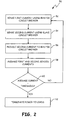
- FIG. 2 is a flowchart illustrating method 50 for digitally summing currents for an electrical system that includes master-slave paralleled circuit breakers.
- master circuit breaker 16a senses a current through shunt resistor 20a.
- Master circuit breaker 16a amplifies the signal and converts the signal to a digital signal using analog-digital converter 28a.
- slave circuit breaker 16b senses a current through shunt resistor 20b.
- Slave circuit breaker 16b amplifies the signal and converts the signal to a digital signal using analog-digital converter 28b.
- slave circuit breaker 16b provides its digital signal to master circuit breaker 16a.
- master circuit breaker 16a averages the digital signal from slave circuit breaker 16b with its own digital signal using digital averager 30a.
- processor 24a determines if the averaged value is greater than a threshold value. If it is, method 50 proceeds to step 62. If it is not, method 50 returns to step 52.
- processor 24a provides a signal to terminate power to load 14. Switches 18a and 18b are opened which terminates power to load 14.
- FIG. 3 is a block diagram illustrating electrical system 110 that includes a plurality of circuit breakers in a master-slave configuration.
- System 110 includes power source 112, load 114, circuit breakers 116a-116d, power switches 118a-118d, and shunt resistors 120a-120d.
- Circuit breaker 116a is configured as the master circuit breaker and circuit breakers 116b-116d are configured as slaves.
- Each circuit breaker 116a-116d senses the current through respective shunt resistors 120a-120d.
- Slave circuit breaker 116c receives a digital current value from slave circuit breaker 116d and performs a bitwise average on the value from circuit breaker 116d and its own digital current value.
- Slave circuit breaker 116b performs a bitwise average on its own digital current value and the average value from circuit breaker 116c.
- Master circuit breaker 116a performs a bitwise average on its own digital current value and the bitwise average value from circuit breaker 116b. While illustrated as four circuit breakers, any number of circuit breakers can be implemented in system 110.
- the ⁇ average> equation determines a bit value to be sent to the next circuit breaker if being calculated by one of slave circuit breakers 116b-116d, or the final average value if being calculated by master circuit breaker 116a.
- the received bit value ⁇ ser_val> from the previous slave circuit breaker is multiplied with the number of slave circuit breaker values already averaged in this bit stream ( ⁇ ser_count>). For example, if circuit breaker 116a is performing the average, ⁇ ser_count> would be three because the bit stream value ⁇ ser_val> received is the average of slaves 116b, 116c and 116d.
- the number of slave circuit breaker values already averaged is determined and sent by software to the present circuit breaker.
- the ⁇ carry> equation now uses the result of the ⁇ average> equation and stores the difference between the summed present value and the number of previous circuit breakers that have contributed to the average bit stream.
- the ⁇ carry> value is used to ensure there is not a significant rounding error, which would reduce the accuracy of the value reported.
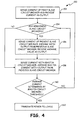
- FIG. 4 is a flowchart illustrating method 150 for digitally summing currents for an electrical system that includes master-slave paralleled circuit breakers with multiple slave circuit breakers.
- a first slave circuit breaker such as circuit breaker 116d of FIG. 3 , senses a current and provides the current as an output.
- the present slave circuit breaker senses its corresponding current, and averages its sensed current with the output of the previous slave circuit breaker. The present slave circuit breaker provides the average current as an output.
- Method 150 returns to step 154 following step 156.
- master circuit breaker 116a senses its corresponding current, and averages its sensed current with the output of the previous slave circuit breaker.
- step 160 if the average current determined by master circuit breaker 116a is greater than a threshold value, method 150 proceeds to step 162. If the average current is not greater than a threshold value, method 150 returns to step 152. At step 162, power to load 114 is terminated by circuit breakers 116a-116d.
- An electrical system may include, among other things: a first circuit breaker that digitally senses a first current to a first load, and a second circuit breaker that digitally senses a second current to a second load and provides an output to the first circuit breaker.
- the first circuit breaker digitally determines an average current based upon the first sensed current and the output of the second circuit breaker.
- the first and second circuit breakers terminate power to the first and second loads if the average current is greater than a threshold value.
- the electrical system of the preceding paragraph can optionally include, additionally and/or alternatively, any one or more of the following features, configurations and/or additional components:
- the analog-to-digital converter may be a sigma-delta converter that converts an analog voltage into a digital bit stream.
- the digital averager of the first circuit breaker may receive a first bit stream from the sigma-delta converter of the first circuit breaker, and a second bit stream from the second circuit breaker.
- the digital averager of the first circuit breaker may output an average bit stream based upon the first and second bit streams.
- the average bit stream from the digital averager of the first circuit breaker may be provided to the processor of the first circuit breaker.
- the processor of the first circuit breaker may determine if the average bit stream represents an average current greater than the threshold value.
- the processor of the first circuit breaker may terminate power to the first load and may provide an indication to the processor of the second circuit breaker to terminate power to the second load.
- the first and second circuit breakers further may include a clock generator. An output of the clock generator of the first circuit breaker may be provided to the second circuit breaker for synchronization.
- a third circuit breaker may be provided that digitally senses a third current to a third load and provides an output to the second circuit breaker.
- the output of the second circuit breaker is an average of the second sensed current and the output of the third circuit breaker.
- a method may include, among other things: sensing a first current using a first circuit breaker, sensing a second current using a second circuit breaker, providing an output from the second circuit breaker to the first circuit breaker, averaging the first sensed current and the output from the second circuit breaker to determine a digital average current, and terminating power to first and second loads if the digital average current is greater than a threshold value.
- Sensing a first current may include amplifying a first voltage across a first shunt resistor and converting the first voltage into a first digital signal.
- Sensing a second current may include amplifying a second voltage across a second shunt resistor and converting the second voltage into a second digital signal.
- Averaging the first sensed current and the output from the second circuit breaker may include averaging the first digital signal and the second digital signal using a bit stream averager of the first circuit breaker.
- Terminating power to first and second loads may include a processor of the first circuit breaker sending a terminate signal to both a gate driver of a first power switch, and the second circuit breaker.
- Terminating power to the first and second loads further may include a processor of the second circuit breaker sending a terminate signal to a gate driver of a second power switch based upon the terminate signal from the processor of the first circuit breaker.
- a master circuit breaker may include, among other things: an analog-to-digital converter that converts an analog voltage into a first digital voltage, an input that receives a second digital voltage from a slave circuit breaker, a bit-stream averager that determines an average voltage from the first digital voltage and the second digital voltage, and an output control signal that indicates when the average voltage is greater than a threshold value.
- the master circuit breaker of the preceding paragraph can optionally include, additionally and/or alternatively, any one or more of the following features, configurations and/or additional components:
- the output control signal may be provided to the slave circuit breaker and a gate driver of a first power switch.
- a clock generator that generates an output that is provided to the analog-to-digital converter and the slave circuit breaker.
Landscapes
- Emergency Protection Circuit Devices (AREA)
Abstract
Description
- Circuit breakers are used to protect electrical systems in case of overcurrent conditions which can be caused by, for example, short circuits or broken loads. Traditionally, circuit breakers were mechanical switches that would open upon detection of an overcurrent condition. Recently, in place of the traditional mechanical switches, electronic devices such as metal-oxide-semiconductor field-effect transistor (MOSFET) power switches have been implemented.
- Multiple circuit breakers are often implemented to accommodate multiple loads. They can either be used as stand-alone circuit breakers, or in parallel to form a higher tolerance breaker. If used in parallel, the circuit breakers must share current between one another. Ideally, for example, two five amp circuit breakers would combine to form a ten amp circuit breaker when connected in parallel. In practice, however, unequal current sharing due to internal tolerancing often results in one breaker that draws more current than the other, and thus trips earlier. This leads to the parallel circuit breakers providing a higher than desired tolerance.
- A master circuit breaker according to an embodiment comprises: a first circuit breaker that digitally senses a first current to a first load; and an input that receives a second digital signal from a slave circuit breaker. The first circuit breaker digitally determines an average current based upon the sensed first current and the second digital signal; and the first circuit breaker outputs an output control signal that indicates when the average current is greater than a threshold value.
- An electrical system according to an embodiment comprises: a master circuit breaker as outlined above; and a slave circuit breaker comprising a second circuit breaker that digitally senses a second current to a second load and provides an output to the first circuit breaker. The first circuit breaker digitally determines an average current based upon the first sensed current and the output of the second circuit breaker; and the first and second circuit breakers terminate power to the first and second loads if the average current is greater than a threshold value.
-
-
FIG. 1 is a circuit diagram illustrating an electrical system that includes master-slave paralleled circuit breakers. -
FIG. 2 is a flowchart illustrating a method for digitally summing currents for an electrical system that includes master-slave paralleled circuit breakers. -
FIG. 3 is a block diagram illustrating a plurality of circuit breakers in a master-slave configuration. -
FIG. 4 is a flowchart illustrating a method for digitally summing currents for an electrical system that includes master-slave paralleled circuit breakers with multiple slave circuit breakers. - The present invention is related to electric systems, and in particular to parallel electronic circuit breakers. Two or more electronic circuit breakers may be used stand-alone or in parallel. Each circuit breaker includes current sensing through the use of a shunt resistor. The sensed current in the form of a voltage across the shunt resistor is amplified and converted into a digital bit-stream using a sigma-delta converter. Each circuit breaker includes a bit stream averager, and the breaker that is designated as the master uses its bit stream averager to average its own sensed current bit stream with the sensed current bit stream of the slave circuit breaker. A processor of the master circuit breaker determines if the average bit stream represents an average current to the loads that is greater than a threshold value. If so, the master circuit breaker terminates power to its load, and provides an indication to the slave circuit breaker to do the same. Any number of circuit breakers can be connected in this way. If connecting more than two circuit breakers in parallel, the bit stream of each slave is averaged to the bit stream of the previous slave.
-
FIG. 1 is a circuit diagram illustratingelectrical system 10 that includes master-slave paralleled circuit breakers.System 10 includespower source 12,load 14,circuit breakers power switches shunt resistors gate drivers Circuit breaker 16a includesprocessor 24a,amplifier 26a, analog-digital converter 28a,digital averager 30a,clock generator 32a,inputs 34a, 36a, and 38a, andoutputs Circuit breaker 16b includesprocessor 24b,amplifier 26b, analog-digital converter 28b,digital averager 30b,clock generator 32b,inputs outputs 44b. Power source 12 is any known AC or DC power source.Power source 12 provides power to load 14 throughpower switches Circuit breakers control power switches - In the present embodiment,
circuit breaker 16a is configured as the master circuit breaker, andcircuit breaker 16b is configured as the slave circuit breaker. In other embodiments,circuit breakers circuit breaker 16b could be configured as the master circuit breaker withcircuit breaker 16a as the slave. -
Circuit breakers shunt resistors Circuit breaker 16a receives the voltage acrossshunt resistor 20a and amplifies it usingamplifier 26a. Analog-to-digital converter 28a converts the amplified voltage fromamplifier 26a into, for example, a digital bit stream. The bit stream is provided tobit stream averager 30a. Amplifier 26a is any known electronic amplifier, and analog-to-digital converter 28a is any known analog-to-digital converter such as, for example, a sigma-delta converter. A sigma-delta converter uses error feedback to generate a bit stream with a given time period. This bit stream is representative of the analog input. -
Circuit breaker 16b receives the voltage acrossshunt resistor 20b and amplifies it usingamplifier 26b. Analog-to-digial converter 28b converts the amplified voltage fromamplifier 26b into a digital bit stream. Amplifier 26b is any known electronic amplifier, and analog-to-digital converter 28b is any known analog-to-digital converter such as, for example, a sigma-delta converter. Becausecircuit breaker 16b is the slave circuit breaker, the bit stream from analog-to-digital converter 28b is provided onoutput 42b tobit stream averager 30a on input 36a ofcircuit breaker 16a. For synchronization purposes, each circuit breaker utilizes the same clock. For example, the output ofclock generator 32a may be provided onoutput 44a to input 38b ofcircuit breaker 16b. Analog-to-digital converter 28b may then, for example, run off the clock fromcircuit breaker 16a. -
Digital averager 30a averages the digital values provided by analog-to-digital converters digital averager 30a performs bit stream averaging with carry to provide a bit stream average. Bit stream averaging with carry is performed on each bit of the two bit streams. Each bit of the bit stream from analog-to-digital converter 28a is averaged with each bit of the bit stream from analog-to-digital converter 28b for the given period of the bit streams. The result is an average bit stream with the same period as the input bit streams. - The average bit stream is provided to
processor 24a.Processor 24a knows the period of the bit stream and can therefore determine the average current sensed between the two circuit breakers based upon the average bit stream.Processor 24a then determines if the average sensed current is greater than a threshold value. The threshold value is set to any value that corresponds to a desired greatest amount of allowable total current to load 14. - If the average current sensed is greater than the threshold value,
processor 24a provides a terminate signal onoutput 40a to bothgate driver 22a andinput 34b ofslave circuit breaker 16b.Processor 24b receives the terminate signal frominput 34b and provides a terminate signal onoutput 40b togate driver 22b.Gate drivers open switches Switches 18a-18b are any electronic switches such as, for example, metal-oxide-semiconductor field-effect transistor (MOSFET) power switches.Switches -
FIG. 2 is a flowchartillustrating method 50 for digitally summing currents for an electrical system that includes master-slave paralleled circuit breakers. Atstep 52,master circuit breaker 16a senses a current throughshunt resistor 20a.Master circuit breaker 16a amplifies the signal and converts the signal to a digital signal using analog-digital converter 28a. Atstep 54,slave circuit breaker 16b senses a current throughshunt resistor 20b.Slave circuit breaker 16b amplifies the signal and converts the signal to a digital signal using analog-digital converter 28b. Atstep 56,slave circuit breaker 16b provides its digital signal tomaster circuit breaker 16a. Atstep 58,master circuit breaker 16a averages the digital signal fromslave circuit breaker 16b with its own digital signal usingdigital averager 30a. Atstep 60,processor 24a determines if the averaged value is greater than a threshold value. If it is,method 50 proceeds to step 62. If it is not,method 50 returns to step 52. Atstep 62,processor 24a provides a signal to terminate power to load 14.Switches -
FIG. 3 is a block diagram illustrating electrical system 110 that includes a plurality of circuit breakers in a master-slave configuration. System 110 includespower source 112,load 114,circuit breakers 116a-116d,power switches 118a-118d, andshunt resistors 120a-120d. Circuit breaker 116a is configured as the master circuit breaker andcircuit breakers 116b-116d are configured as slaves. Eachcircuit breaker 116a-116d senses the current throughrespective shunt resistors 120a-120d.Slave circuit breaker 116c receives a digital current value fromslave circuit breaker 116d and performs a bitwise average on the value fromcircuit breaker 116d and its own digital current value.Slave circuit breaker 116b performs a bitwise average on its own digital current value and the average value fromcircuit breaker 116c.Master circuit breaker 116a performs a bitwise average on its own digital current value and the bitwise average value fromcircuit breaker 116b. While illustrated as four circuit breakers, any number of circuit breakers can be implemented in system 110. - Bit stream averaging by
slave circuit breakers 116b-116d and bymaster circuit breaker 116a may be performed using the following equations:

- <average>: Average bit stream value determined by the present circuit breaker;
- <carry>: Memorized rounding error to be considered during the next average bit stream value calculation;
- <ser_count>: Number of bit stream values already averaged by previous circuit breakers for the present input average data stream;
- <ser_val>: Present bit of the serial input data stream;
- <i_val>: Sensed current bit measured by the present circuit breaker.
- The <average> equation determines a bit value to be sent to the next circuit breaker if being calculated by one of
slave circuit breakers 116b-116d, or the final average value if being calculated bymaster circuit breaker 116a. The received bit value <ser_val> from the previous slave circuit breaker is multiplied with the number of slave circuit breaker values already averaged in this bit stream (<ser_count>). For example, ifcircuit breaker 116a is performing the average, <ser_count> would be three because the bit stream value <ser_val> received is the average ofslaves - The <carry> equation now uses the result of the <average> equation and stores the difference between the summed present value and the number of previous circuit breakers that have contributed to the average bit stream. The <carry> value is used to ensure there is not a significant rounding error, which would reduce the accuracy of the value reported.
-
FIG. 4 is aflowchart illustrating method 150 for digitally summing currents for an electrical system that includes master-slave paralleled circuit breakers with multiple slave circuit breakers. Atstep 152, a first slave circuit breaker, such ascircuit breaker 116d ofFIG. 3 , senses a current and provides the current as an output. Atstep 154, it is determined if any slave circuit breakers remain. If any slave circuit breakers remain,method 150 proceeds to step 156. If no slave circuit breakers remain,method 150 proceeds to step 158. Atstep 156, the present slave circuit breaker senses its corresponding current, and averages its sensed current with the output of the previous slave circuit breaker. The present slave circuit breaker provides the average current as an output.Method 150 returns to step 154 followingstep 156. Atstep 158,master circuit breaker 116a senses its corresponding current, and averages its sensed current with the output of the previous slave circuit breaker. Atstep 160, if the average current determined bymaster circuit breaker 116a is greater than a threshold value,method 150 proceeds to step 162. If the average current is not greater than a threshold value,method 150 returns to step 152. Atstep 162, power to load 114 is terminated bycircuit breakers 116a-116d. - The following are non-exclusive descriptions of possible embodiments of the present invention.
- An electrical system may include, among other things: a first circuit breaker that digitally senses a first current to a first load, and a second circuit breaker that digitally senses a second current to a second load and provides an output to the first circuit breaker. The first circuit breaker digitally determines an average current based upon the first sensed current and the output of the second circuit breaker. The first and second circuit breakers terminate power to the first and second loads if the average current is greater than a threshold value.
- The electrical system of the preceding paragraph can optionally include, additionally and/or alternatively, any one or more of the following features, configurations and/or additional components:
- The first and second circuit breakers each may include an analog-to-digital converter, a digital averager, and a processor.
- The analog-to-digital converter may be a sigma-delta converter that converts an analog voltage into a digital bit stream.
- The digital averager of the first circuit breaker may receive a first bit stream from the sigma-delta converter of the first circuit breaker, and a second bit stream from the second circuit breaker. The digital averager of the first circuit breaker may output an average bit stream based upon the first and second bit streams.
- The average bit stream from the digital averager of the first circuit breaker may be provided to the processor of the first circuit breaker. The processor of the first circuit breaker may determine if the average bit stream represents an average current greater than the threshold value.
- If the average current is greater than the threshold value, the processor of the first circuit breaker may terminate power to the first load and may provide an indication to the processor of the second circuit breaker to terminate power to the second load.
- The first and second circuit breakers further may include a clock generator. An output of the clock generator of the first circuit breaker may be provided to the second circuit breaker for synchronization.
- A third circuit breaker may be provided that digitally senses a third current to a third load and provides an output to the second circuit breaker. The output of the second circuit breaker is an average of the second sensed current and the output of the third circuit breaker.
- A method may include, among other things: sensing a first current using a first circuit breaker, sensing a second current using a second circuit breaker, providing an output from the second circuit breaker to the first circuit breaker, averaging the first sensed current and the output from the second circuit breaker to determine a digital average current, and terminating power to first and second loads if the digital average current is greater than a threshold value.
- Sensing a first current may include amplifying a first voltage across a first shunt resistor and converting the first voltage into a first digital signal.
- Sensing a second current may include amplifying a second voltage across a second shunt resistor and converting the second voltage into a second digital signal.
Averaging the first sensed current and the output from the second circuit breaker may include averaging the first digital signal and the second digital signal using a bit stream averager of the first circuit breaker. - Terminating power to first and second loads may include a processor of the first circuit breaker sending a terminate signal to both a gate driver of a first power switch, and the second circuit breaker.
- Terminating power to the first and second loads further may include a processor of the second circuit breaker sending a terminate signal to a gate driver of a second power switch based upon the terminate signal from the processor of the first circuit breaker.
- A master circuit breaker may include, among other things: an analog-to-digital converter that converts an analog voltage into a first digital voltage, an input that receives a second digital voltage from a slave circuit breaker, a bit-stream averager that determines an average voltage from the first digital voltage and the second digital voltage, and an output control signal that indicates when the average voltage is greater than a threshold value.
- The master circuit breaker of the preceding paragraph can optionally include, additionally and/or alternatively, any one or more of the following features, configurations and/or additional components:
- A processor that determines if the average voltage is greater than the threshold value.
- The output control signal may be provided to the slave circuit breaker and a gate driver of a first power switch.
- A clock generator that generates an output that is provided to the analog-to-digital converter and the slave circuit breaker.
- An amplifier that amplifies the analog voltage for the analog-to-digital converter.
While the invention has been described with reference to an exemplary embodiment(s), it will be understood by those skilled in the art that various changes may be made and equivalents may be substituted for elements thereof without departing from the scope of the invention. In addition, many modifications may be made to adapt a particular situation or material to the teachings of the invention without departing from the essential scope thereof. Therefore, it is intended that the invention not be limited to the particular embodiment(s) disclosed, but that the invention will include all embodiments falling within the scope of the appended claims.
Claims (15)
- A master circuit breaker comprising:a first circuit breaker (16a; 116a) that digitally senses a first current to a first load (14; 114); andan input that receives a second digital signal from a slave circuit breaker;wherein the first circuit breaker (16a; 116a) digitally determines an average current based upon the sensed first current and the second digital signal; andwherein the first circuit breaker outputs an output control signal that indicates when the average current is greater than a threshold value.
- The master circuit breaker of claim 1, further comprising:an analog-to-digital converter (28a) that converts an analog voltage into a first digital voltage;a bit-stream averager (30a) that determines said average voltage from the first digital voltage and the second digital voltage; anda processor (24a) that determines if the average voltage is greater than the threshold value.
- The master circuit breaker of claim 1 or 2, wherein the output control signal is provided to the slave circuit breaker and a gate driver (22a) of a first power switch (18a).
- The master circuit breaker of claim 3, further comprising a clock generator (32a) that generates an output that is provided to the analog-to-digital converter (28a) and the slave circuit breaker; particularly further comprising an amplifier (26a) that amplifies the analog voltage for the analog-to-digital converter (28a).
- An electrical system comprising:a master circuit breaker according to any of the previous claims,a slave circuit breaker comprising a second circuit breaker (16b; 116b) that digitally senses a second current to a second load and provides an output (42b) to the first circuit breaker (16a; 116a);wherein the first circuit breaker (16a; 116a) digitally determines an average current based upon the first sensed current and the output of the second circuit breaker (16b: 116b); andwherein the first and second circuit breakers (16a, 16b; 116a, 116b) terminate power to the first and second loads if the average current is greater than a threshold value.
- The system of claim 5, wherein the first and second circuit breakers (16a, 16b; 116a, 116b) each comprise:an analog-to-digital converter (28a, 28b), particularly a sigma-delta converter that converts an analog voltage into a digital bit stream;a digital averager(30a, 30b); anda processor (24a, 24b);
- The system of claim 6, wherein the digital averager (30a) of the first circuit breaker (16a; 116a) receives a first bit stream from the sigma-delta converter (28a) of the first circuit breaker (16a; 116a), and a second bit stream from the second circuit breaker (16b; 116b), and wherein the digital averager (30a) of the first circuit breaker (16a; 116a) outputs an average bit stream based upon the first and second bit streams; the average bit stream from the digital averager (30a) of the first circuit breaker (16a; 116a) particularly being provided to the processor (24a) of the first circuit breaker (16a; 116a), the processor (24a) of the first circuit breaker (16a; 116) determining if the average bit stream represents an average current greater than the threshold value.
- The system of claim 7, wherein if the average current is greater than the threshold value, the processor (24a) of the first circuit breaker (16a; 116a) terminates power to the first load (14; 114) and provides an indication to the processor (30b) of the second circuit breaker (16b; 116b) to terminate power to the second load (14; 114).
- The system of any of claims 6 to 8, wherein the first and second circuit breakers (16a, 16b; 116a, 116b) further comprise a clock generator (32a, 32b), and wherein an output of the clock generator (32a) f the first circuit breaker (16a; 116a) is provided to the second circuit breaker (16b; 116b) for synchronization.
- The system of any of claims 6 to 9, further comprising:a third circuit breaker (116c) that digitally senses a third current to a third load (114) and provides an output to the second circuit breaker (116b); andwherein the output of the second circuit breaker (116b) is an average of the second sensed current and the output of the third circuit breaker (116c).
- A method comprising:digitally sensing a first current using a master circuit breaker comprising a first circuit breaker (16a; 116a);receiving a second digital signal from a slave circuit breaker;digitally determining an average current based upon the sensed first current and the second digital signal; andproviding an output signal that indicates when the average current is greater than a threshold value.
- The method of claim 11, further comprisingdigitally sensing a second current using a second circuit breaker (16b; 116b);providing an output from the second circuit breaker (16b; 116b) as the second digital signal to the first circuit breaker (16a; 116a); andterminating power to first and second loads (14; 114) if the average current is greater than a threshold value.
- The method of claim 11 or 12, wherein sensing a first current comprises amplifying a first voltage across a first shunt resistor (20a; 120a) and converting the first voltage into a first digital signal; and/or wherein sensing a second current comprises amplifying a second voltage across a second shunt resistor (20a; 120a) and converting the second voltage into a second digital signal.
- The method of claim 13, wherein averaging the first sensed current and the output from the second circuit breaker (16b; 116b) comprises averaging the first digital signal and the second digital signal using a bit stream averager (30a) of the first circuit breaker (16a; 116a).
- The method of claim 13, wherein terminating power to first and second loads (14; 114) comprises a processor (24a) of the first circuit breaker (16a; 116a) sending a terminate signal to both a gate driver (22a) of a first power switch (18a), and the second circuit breaker (16b; 116b); and/or wherein terminating power to the first and second loads (14; 114) further comprises a processor (24b) of the second circuit breaker (16b; 116b) sending a terminate signal to a gate driver (22b) of a second power switch (18b) based upon the terminate signal from the processor (24a) of the first circuit breaker (16a; 116a).
Applications Claiming Priority (1)
| Application Number | Priority Date | Filing Date | Title |
|---|---|---|---|
| DE102013103020.3A DE102013103020A1 (en) | 2013-03-25 | 2013-03-25 | Digital master-slave circuit breaker |
Publications (2)
| Publication Number | Publication Date |
|---|---|
| EP2784890A1 true EP2784890A1 (en) | 2014-10-01 |
| EP2784890B1 EP2784890B1 (en) | 2019-09-04 |
Family
ID=50336193
Family Applications (1)
| Application Number | Title | Priority Date | Filing Date |
|---|---|---|---|
| EP14161032.9A Active EP2784890B1 (en) | 2013-03-25 | 2014-03-21 | Master-slave digital circuit breakers |
Country Status (3)
| Country | Link |
|---|---|
| US (1) | US9466969B2 (en) |
| EP (1) | EP2784890B1 (en) |
| DE (1) | DE102013103020A1 (en) |
Cited By (2)
| Publication number | Priority date | Publication date | Assignee | Title |
|---|---|---|---|---|
| EP3176903A3 (en) * | 2015-12-04 | 2017-06-21 | HS Elektronik Systeme GmbH | Power distribution system |
| EP3389185A1 (en) * | 2017-04-11 | 2018-10-17 | HS Elektronik Systeme GmbH | Solid state power controller |
Families Citing this family (3)
| Publication number | Priority date | Publication date | Assignee | Title |
|---|---|---|---|---|
| KR101673786B1 (en) * | 2015-07-02 | 2016-11-07 | 현대자동차주식회사 | System and method for connecting external device with vehicle |
| CN117859248A (en) * | 2021-06-11 | 2024-04-09 | 氦核能源有限公司 | High-speed switching device for electromagnetic coil |
| US12489452B2 (en) | 2022-11-15 | 2025-12-02 | Renesas Design (UK) Limited | Method of correcting a data stream of a pulse density modulator |
Citations (2)
| Publication number | Priority date | Publication date | Assignee | Title |
|---|---|---|---|---|
| US20030189804A1 (en) * | 2002-04-04 | 2003-10-09 | Kampmeyer Roy A. | Ground fault circuit interrupter |
| GB2438712A (en) * | 2006-05-31 | 2007-12-05 | Natali Gianfranco | Device for breaking and closing electric circuits |
Family Cites Families (3)
| Publication number | Priority date | Publication date | Assignee | Title |
|---|---|---|---|---|
| US4972290A (en) * | 1989-09-29 | 1990-11-20 | Abb Power T & D Company Inc. | Electric power system with remote monitoring and control of protective relays |
| JP3284589B2 (en) * | 1992-06-01 | 2002-05-20 | 株式会社日立製作所 | Transmission line protection method and protection relay device |
| EP2015341B1 (en) * | 2007-07-10 | 2010-01-20 | Siemens Aktiengesellschaft | Group insulation module for a switching gear assembly and switching gear assembly with such a group insulation module |
-
2013
- 2013-03-25 DE DE102013103020.3A patent/DE102013103020A1/en not_active Withdrawn
-
2014
- 2014-03-21 EP EP14161032.9A patent/EP2784890B1/en active Active
- 2014-03-24 US US14/223,781 patent/US9466969B2/en active Active
Patent Citations (2)
| Publication number | Priority date | Publication date | Assignee | Title |
|---|---|---|---|---|
| US20030189804A1 (en) * | 2002-04-04 | 2003-10-09 | Kampmeyer Roy A. | Ground fault circuit interrupter |
| GB2438712A (en) * | 2006-05-31 | 2007-12-05 | Natali Gianfranco | Device for breaking and closing electric circuits |
Non-Patent Citations (1)
| Title |
|---|
| IVAN BERNARD FULLER: "SCHEMES FOR REDUNDANCY BY INFORMATION EXCHANGE BETWEEN RELAYS IN POWER SYSTEM", IP.COM JOURNAL, IP.COM INC., WEST HENRIETTA, NY, US, 29 June 2012 (2012-06-29), XP013152298, ISSN: 1533-0001 * |
Cited By (3)
| Publication number | Priority date | Publication date | Assignee | Title |
|---|---|---|---|---|
| EP3176903A3 (en) * | 2015-12-04 | 2017-06-21 | HS Elektronik Systeme GmbH | Power distribution system |
| EP3389185A1 (en) * | 2017-04-11 | 2018-10-17 | HS Elektronik Systeme GmbH | Solid state power controller |
| US10923920B2 (en) | 2017-04-11 | 2021-02-16 | Hs Elektronik System Gmbh | Solid state power controller |
Also Published As
| Publication number | Publication date |
|---|---|
| DE102013103020A1 (en) | 2014-09-25 |
| US9466969B2 (en) | 2016-10-11 |
| US20140285940A1 (en) | 2014-09-25 |
| EP2784890B1 (en) | 2019-09-04 |
Similar Documents
| Publication | Publication Date | Title |
|---|---|---|
| US9466969B2 (en) | Master-slave digital circuit breakers | |
| US8779784B2 (en) | Insulation resistance measuring circuit free from influence of battery voltage | |
| EP2953225B1 (en) | Method of detection and isolation of faults within power conversion and distribution systems | |
| CN109478773B (en) | Arc fault identification unit | |
| US7309993B2 (en) | Three- or four-pole low-voltage power switch with Rogowski coils operating as current sensors | |
| JP7285757B2 (en) | Protective relay device | |
| WO2015189996A1 (en) | Digital protection relay | |
| EP3389185A1 (en) | Solid state power controller | |
| EP3179257B1 (en) | Precise current measurement with chopping technique for high power driver | |
| EP2767839B1 (en) | Root mean square detector and circuit breaker using the same | |
| JP6180346B2 (en) | Protective relay device | |
| EP4340215B1 (en) | Motor drive direct current link voltage measurement resolution improvement with fault detection | |
| JP2001141753A (en) | Current and electric quantity measuring circuit | |
| JP7102626B2 (en) | Methods and devices for current and voltage measurement | |
| EP4062535B1 (en) | Overcurrent detector | |
| RU2321002C1 (en) | Current transducer | |
| US11784486B2 (en) | Low-voltage circuit breaker and power measuring arrangement | |
| EP4648289A1 (en) | Overcurrent detection with multi-bit analog-to-digital converters | |
| US12418168B2 (en) | High-impedance differential protection using a diversity of signals | |
| KR101514248B1 (en) | Power equipment for preventing mal-operation | |
| US20240421711A1 (en) | Current sharing of bidirectional converters connected in parallel | |
| JP2005057927A (en) | Controller for digital protective relay | |
| KR100364821B1 (en) | Apparatus for transform signal of current transformer | |
| JP4103789B2 (en) | Protection control device | |
| CN121307773A (en) | Electronic safety device |
Legal Events
| Date | Code | Title | Description |
|---|---|---|---|
| 17P | Request for examination filed |
Effective date: 20140321 |
|
| AK | Designated contracting states |
Kind code of ref document: A1 Designated state(s): AL AT BE BG CH CY CZ DE DK EE ES FI FR GB GR HR HU IE IS IT LI LT LU LV MC MK MT NL NO PL PT RO RS SE SI SK SM TR |
|
| AX | Request for extension of the european patent |
Extension state: BA ME |
|
| PUAI | Public reference made under article 153(3) epc to a published international application that has entered the european phase |
Free format text: ORIGINAL CODE: 0009012 |
|
| R17P | Request for examination filed (corrected) |
Effective date: 20150330 |
|
| RBV | Designated contracting states (corrected) |
Designated state(s): AL AT BE BG CH CY CZ DE DK EE ES FI FR GB GR HR HU IE IS IT LI LT LU LV MC MK MT NL NO PL PT RO RS SE SI SK SM TR |
|
| 17Q | First examination report despatched |
Effective date: 20151203 |
|
| GRAP | Despatch of communication of intention to grant a patent |
Free format text: ORIGINAL CODE: EPIDOSNIGR1 |
|
| STAA | Information on the status of an ep patent application or granted ep patent |
Free format text: STATUS: GRANT OF PATENT IS INTENDED |
|
| INTG | Intention to grant announced |
Effective date: 20190401 |
|
| GRAS | Grant fee paid |
Free format text: ORIGINAL CODE: EPIDOSNIGR3 |
|
| GRAA | (expected) grant |
Free format text: ORIGINAL CODE: 0009210 |
|
| STAA | Information on the status of an ep patent application or granted ep patent |
Free format text: STATUS: THE PATENT HAS BEEN GRANTED |
|
| AK | Designated contracting states |
Kind code of ref document: B1 Designated state(s): AL AT BE BG CH CY CZ DE DK EE ES FI FR GB GR HR HU IE IS IT LI LT LU LV MC MK MT NL NO PL PT RO RS SE SI SK SM TR |
|
| REG | Reference to a national code |
Ref country code: GB Ref legal event code: FG4D |
|
| REG | Reference to a national code |
Ref country code: CH Ref legal event code: EP |
|
| REG | Reference to a national code |
Ref country code: AT Ref legal event code: REF Ref document number: 1176717 Country of ref document: AT Kind code of ref document: T Effective date: 20190915 |
|
| REG | Reference to a national code |
Ref country code: DE Ref legal event code: R096 Ref document number: 602014052833 Country of ref document: DE |
|
| REG | Reference to a national code |
Ref country code: IE Ref legal event code: FG4D |
|
| REG | Reference to a national code |
Ref country code: NL Ref legal event code: MP Effective date: 20190904 |
|
| REG | Reference to a national code |
Ref country code: LT Ref legal event code: MG4D |
|
| PG25 | Lapsed in a contracting state [announced via postgrant information from national office to epo] |
Ref country code: FI Free format text: LAPSE BECAUSE OF FAILURE TO SUBMIT A TRANSLATION OF THE DESCRIPTION OR TO PAY THE FEE WITHIN THE PRESCRIBED TIME-LIMIT Effective date: 20190904 Ref country code: NO Free format text: LAPSE BECAUSE OF FAILURE TO SUBMIT A TRANSLATION OF THE DESCRIPTION OR TO PAY THE FEE WITHIN THE PRESCRIBED TIME-LIMIT Effective date: 20191204 Ref country code: HR Free format text: LAPSE BECAUSE OF FAILURE TO SUBMIT A TRANSLATION OF THE DESCRIPTION OR TO PAY THE FEE WITHIN THE PRESCRIBED TIME-LIMIT Effective date: 20190904 Ref country code: LT Free format text: LAPSE BECAUSE OF FAILURE TO SUBMIT A TRANSLATION OF THE DESCRIPTION OR TO PAY THE FEE WITHIN THE PRESCRIBED TIME-LIMIT Effective date: 20190904 Ref country code: SE Free format text: LAPSE BECAUSE OF FAILURE TO SUBMIT A TRANSLATION OF THE DESCRIPTION OR TO PAY THE FEE WITHIN THE PRESCRIBED TIME-LIMIT Effective date: 20190904 Ref country code: BG Free format text: LAPSE BECAUSE OF FAILURE TO SUBMIT A TRANSLATION OF THE DESCRIPTION OR TO PAY THE FEE WITHIN THE PRESCRIBED TIME-LIMIT Effective date: 20191204 |
|
| PG25 | Lapsed in a contracting state [announced via postgrant information from national office to epo] |
Ref country code: GR Free format text: LAPSE BECAUSE OF FAILURE TO SUBMIT A TRANSLATION OF THE DESCRIPTION OR TO PAY THE FEE WITHIN THE PRESCRIBED TIME-LIMIT Effective date: 20191205 Ref country code: LV Free format text: LAPSE BECAUSE OF FAILURE TO SUBMIT A TRANSLATION OF THE DESCRIPTION OR TO PAY THE FEE WITHIN THE PRESCRIBED TIME-LIMIT Effective date: 20190904 Ref country code: AL Free format text: LAPSE BECAUSE OF FAILURE TO SUBMIT A TRANSLATION OF THE DESCRIPTION OR TO PAY THE FEE WITHIN THE PRESCRIBED TIME-LIMIT Effective date: 20190904 Ref country code: RS Free format text: LAPSE BECAUSE OF FAILURE TO SUBMIT A TRANSLATION OF THE DESCRIPTION OR TO PAY THE FEE WITHIN THE PRESCRIBED TIME-LIMIT Effective date: 20190904 Ref country code: ES Free format text: LAPSE BECAUSE OF FAILURE TO SUBMIT A TRANSLATION OF THE DESCRIPTION OR TO PAY THE FEE WITHIN THE PRESCRIBED TIME-LIMIT Effective date: 20190904 |
|
| REG | Reference to a national code |
Ref country code: AT Ref legal event code: MK05 Ref document number: 1176717 Country of ref document: AT Kind code of ref document: T Effective date: 20190904 |
|
| PG25 | Lapsed in a contracting state [announced via postgrant information from national office to epo] |
Ref country code: IT Free format text: LAPSE BECAUSE OF FAILURE TO SUBMIT A TRANSLATION OF THE DESCRIPTION OR TO PAY THE FEE WITHIN THE PRESCRIBED TIME-LIMIT Effective date: 20190904 Ref country code: RO Free format text: LAPSE BECAUSE OF FAILURE TO SUBMIT A TRANSLATION OF THE DESCRIPTION OR TO PAY THE FEE WITHIN THE PRESCRIBED TIME-LIMIT Effective date: 20190904 Ref country code: PT Free format text: LAPSE BECAUSE OF FAILURE TO SUBMIT A TRANSLATION OF THE DESCRIPTION OR TO PAY THE FEE WITHIN THE PRESCRIBED TIME-LIMIT Effective date: 20200106 Ref country code: AT Free format text: LAPSE BECAUSE OF FAILURE TO SUBMIT A TRANSLATION OF THE DESCRIPTION OR TO PAY THE FEE WITHIN THE PRESCRIBED TIME-LIMIT Effective date: 20190904 Ref country code: NL Free format text: LAPSE BECAUSE OF FAILURE TO SUBMIT A TRANSLATION OF THE DESCRIPTION OR TO PAY THE FEE WITHIN THE PRESCRIBED TIME-LIMIT Effective date: 20190904 Ref country code: PL Free format text: LAPSE BECAUSE OF FAILURE TO SUBMIT A TRANSLATION OF THE DESCRIPTION OR TO PAY THE FEE WITHIN THE PRESCRIBED TIME-LIMIT Effective date: 20190904 Ref country code: EE Free format text: LAPSE BECAUSE OF FAILURE TO SUBMIT A TRANSLATION OF THE DESCRIPTION OR TO PAY THE FEE WITHIN THE PRESCRIBED TIME-LIMIT Effective date: 20190904 |
|
| PG25 | Lapsed in a contracting state [announced via postgrant information from national office to epo] |
Ref country code: CZ Free format text: LAPSE BECAUSE OF FAILURE TO SUBMIT A TRANSLATION OF THE DESCRIPTION OR TO PAY THE FEE WITHIN THE PRESCRIBED TIME-LIMIT Effective date: 20190904 Ref country code: SM Free format text: LAPSE BECAUSE OF FAILURE TO SUBMIT A TRANSLATION OF THE DESCRIPTION OR TO PAY THE FEE WITHIN THE PRESCRIBED TIME-LIMIT Effective date: 20190904 Ref country code: SK Free format text: LAPSE BECAUSE OF FAILURE TO SUBMIT A TRANSLATION OF THE DESCRIPTION OR TO PAY THE FEE WITHIN THE PRESCRIBED TIME-LIMIT Effective date: 20190904 Ref country code: IS Free format text: LAPSE BECAUSE OF FAILURE TO SUBMIT A TRANSLATION OF THE DESCRIPTION OR TO PAY THE FEE WITHIN THE PRESCRIBED TIME-LIMIT Effective date: 20200224 |
|
| REG | Reference to a national code |
Ref country code: DE Ref legal event code: R097 Ref document number: 602014052833 Country of ref document: DE |
|
| PLBE | No opposition filed within time limit |
Free format text: ORIGINAL CODE: 0009261 |
|
| STAA | Information on the status of an ep patent application or granted ep patent |
Free format text: STATUS: NO OPPOSITION FILED WITHIN TIME LIMIT |
|
| PG2D | Information on lapse in contracting state deleted |
Ref country code: IS |
|
| PG25 | Lapsed in a contracting state [announced via postgrant information from national office to epo] |
Ref country code: DK Free format text: LAPSE BECAUSE OF FAILURE TO SUBMIT A TRANSLATION OF THE DESCRIPTION OR TO PAY THE FEE WITHIN THE PRESCRIBED TIME-LIMIT Effective date: 20190904 Ref country code: IS Free format text: LAPSE BECAUSE OF FAILURE TO SUBMIT A TRANSLATION OF THE DESCRIPTION OR TO PAY THE FEE WITHIN THE PRESCRIBED TIME-LIMIT Effective date: 20200105 |
|
| 26N | No opposition filed |
Effective date: 20200605 |
|
| PG25 | Lapsed in a contracting state [announced via postgrant information from national office to epo] |
Ref country code: SI Free format text: LAPSE BECAUSE OF FAILURE TO SUBMIT A TRANSLATION OF THE DESCRIPTION OR TO PAY THE FEE WITHIN THE PRESCRIBED TIME-LIMIT Effective date: 20190904 |
|
| REG | Reference to a national code |
Ref country code: DE Ref legal event code: R119 Ref document number: 602014052833 Country of ref document: DE |
|
| PG25 | Lapsed in a contracting state [announced via postgrant information from national office to epo] |
Ref country code: MC Free format text: LAPSE BECAUSE OF FAILURE TO SUBMIT A TRANSLATION OF THE DESCRIPTION OR TO PAY THE FEE WITHIN THE PRESCRIBED TIME-LIMIT Effective date: 20190904 |
|
| REG | Reference to a national code |
Ref country code: CH Ref legal event code: PL |
|
| REG | Reference to a national code |
Ref country code: BE Ref legal event code: MM Effective date: 20200331 |
|
| PG25 | Lapsed in a contracting state [announced via postgrant information from national office to epo] |
Ref country code: LU Free format text: LAPSE BECAUSE OF NON-PAYMENT OF DUE FEES Effective date: 20200321 |
|
| PG25 | Lapsed in a contracting state [announced via postgrant information from national office to epo] |
Ref country code: CH Free format text: LAPSE BECAUSE OF NON-PAYMENT OF DUE FEES Effective date: 20200331 Ref country code: DE Free format text: LAPSE BECAUSE OF NON-PAYMENT OF DUE FEES Effective date: 20201001 Ref country code: IE Free format text: LAPSE BECAUSE OF NON-PAYMENT OF DUE FEES Effective date: 20200321 Ref country code: LI Free format text: LAPSE BECAUSE OF NON-PAYMENT OF DUE FEES Effective date: 20200331 |
|
| PG25 | Lapsed in a contracting state [announced via postgrant information from national office to epo] |
Ref country code: BE Free format text: LAPSE BECAUSE OF NON-PAYMENT OF DUE FEES Effective date: 20200331 |
|
| PG25 | Lapsed in a contracting state [announced via postgrant information from national office to epo] |
Ref country code: TR Free format text: LAPSE BECAUSE OF FAILURE TO SUBMIT A TRANSLATION OF THE DESCRIPTION OR TO PAY THE FEE WITHIN THE PRESCRIBED TIME-LIMIT Effective date: 20190904 Ref country code: MT Free format text: LAPSE BECAUSE OF FAILURE TO SUBMIT A TRANSLATION OF THE DESCRIPTION OR TO PAY THE FEE WITHIN THE PRESCRIBED TIME-LIMIT Effective date: 20190904 Ref country code: CY Free format text: LAPSE BECAUSE OF FAILURE TO SUBMIT A TRANSLATION OF THE DESCRIPTION OR TO PAY THE FEE WITHIN THE PRESCRIBED TIME-LIMIT Effective date: 20190904 |
|
| PG25 | Lapsed in a contracting state [announced via postgrant information from national office to epo] |
Ref country code: MK Free format text: LAPSE BECAUSE OF FAILURE TO SUBMIT A TRANSLATION OF THE DESCRIPTION OR TO PAY THE FEE WITHIN THE PRESCRIBED TIME-LIMIT Effective date: 20190904 |
|
| P01 | Opt-out of the competence of the unified patent court (upc) registered |
Effective date: 20230522 |
|
| PGFP | Annual fee paid to national office [announced via postgrant information from national office to epo] |
Ref country code: GB Payment date: 20260220 Year of fee payment: 13 |
|
| PGFP | Annual fee paid to national office [announced via postgrant information from national office to epo] |
Ref country code: FR Payment date: 20260219 Year of fee payment: 13 |