EP2784573A1 - Optical device - Google Patents
Optical device Download PDFInfo
- Publication number
- EP2784573A1 EP2784573A1 EP12850856.1A EP12850856A EP2784573A1 EP 2784573 A1 EP2784573 A1 EP 2784573A1 EP 12850856 A EP12850856 A EP 12850856A EP 2784573 A1 EP2784573 A1 EP 2784573A1
- Authority
- EP
- European Patent Office
- Prior art keywords
- wave plate
- light
- polarization
- wavelength
- stacked
- Prior art date
- Legal status (The legal status is an assumption and is not a legal conclusion. Google has not performed a legal analysis and makes no representation as to the accuracy of the status listed.)
- Granted
Links
- 230000003287 optical effect Effects 0.000 title claims abstract description 60
- 230000010287 polarization Effects 0.000 claims abstract description 275
- 230000005540 biological transmission Effects 0.000 claims description 70
- 230000008878 coupling Effects 0.000 claims description 24
- 238000010168 coupling process Methods 0.000 claims description 24
- 238000005859 coupling reaction Methods 0.000 claims description 24
- 210000002858 crystal cell Anatomy 0.000 claims description 12
- 239000004973 liquid crystal related substance Substances 0.000 claims description 12
- 239000000463 material Substances 0.000 claims description 8
- 238000002834 transmittance Methods 0.000 description 35
- 239000000835 fiber Substances 0.000 description 20
- 238000010586 diagram Methods 0.000 description 18
- 230000008859 change Effects 0.000 description 10
- 230000004048 modification Effects 0.000 description 8
- 238000012986 modification Methods 0.000 description 8
- 238000004364 calculation method Methods 0.000 description 4
- 239000006185 dispersion Substances 0.000 description 3
- 230000001419 dependent effect Effects 0.000 description 2
- 230000000694 effects Effects 0.000 description 2
- 238000005516 engineering process Methods 0.000 description 2
- 239000005262 ferroelectric liquid crystals (FLCs) Substances 0.000 description 2
- 239000004988 Nematic liquid crystal Substances 0.000 description 1
- 230000009467 reduction Effects 0.000 description 1
- 230000009466 transformation Effects 0.000 description 1
Images




Classifications
-
- F—MECHANICAL ENGINEERING; LIGHTING; HEATING; WEAPONS; BLASTING
- F21—LIGHTING
- F21V—FUNCTIONAL FEATURES OR DETAILS OF LIGHTING DEVICES OR SYSTEMS THEREOF; STRUCTURAL COMBINATIONS OF LIGHTING DEVICES WITH OTHER ARTICLES, NOT OTHERWISE PROVIDED FOR
- F21V5/00—Refractors for light sources
- F21V5/008—Combination of two or more successive refractors along an optical axis
-
- G—PHYSICS
- G02—OPTICS
- G02B—OPTICAL ELEMENTS, SYSTEMS OR APPARATUS
- G02B27/00—Optical systems or apparatus not provided for by any of the groups G02B1/00 - G02B26/00, G02B30/00
- G02B27/28—Optical systems or apparatus not provided for by any of the groups G02B1/00 - G02B26/00, G02B30/00 for polarising
- G02B27/281—Optical systems or apparatus not provided for by any of the groups G02B1/00 - G02B26/00, G02B30/00 for polarising used for attenuating light intensity, e.g. comprising rotatable polarising elements
-
- G—PHYSICS
- G02—OPTICS
- G02F—OPTICAL DEVICES OR ARRANGEMENTS FOR THE CONTROL OF LIGHT BY MODIFICATION OF THE OPTICAL PROPERTIES OF THE MEDIA OF THE ELEMENTS INVOLVED THEREIN; NON-LINEAR OPTICS; FREQUENCY-CHANGING OF LIGHT; OPTICAL LOGIC ELEMENTS; OPTICAL ANALOGUE/DIGITAL CONVERTERS
- G02F1/00—Devices or arrangements for the control of the intensity, colour, phase, polarisation or direction of light arriving from an independent light source, e.g. switching, gating or modulating; Non-linear optics
- G02F1/01—Devices or arrangements for the control of the intensity, colour, phase, polarisation or direction of light arriving from an independent light source, e.g. switching, gating or modulating; Non-linear optics for the control of the intensity, phase, polarisation or colour
- G02F1/0136—Devices or arrangements for the control of the intensity, colour, phase, polarisation or direction of light arriving from an independent light source, e.g. switching, gating or modulating; Non-linear optics for the control of the intensity, phase, polarisation or colour for the control of polarisation, e.g. state of polarisation [SOP] control, polarisation scrambling, TE-TM mode conversion or separation
-
- G—PHYSICS
- G02—OPTICS
- G02F—OPTICAL DEVICES OR ARRANGEMENTS FOR THE CONTROL OF LIGHT BY MODIFICATION OF THE OPTICAL PROPERTIES OF THE MEDIA OF THE ELEMENTS INVOLVED THEREIN; NON-LINEAR OPTICS; FREQUENCY-CHANGING OF LIGHT; OPTICAL LOGIC ELEMENTS; OPTICAL ANALOGUE/DIGITAL CONVERTERS
- G02F1/00—Devices or arrangements for the control of the intensity, colour, phase, polarisation or direction of light arriving from an independent light source, e.g. switching, gating or modulating; Non-linear optics
- G02F1/01—Devices or arrangements for the control of the intensity, colour, phase, polarisation or direction of light arriving from an independent light source, e.g. switching, gating or modulating; Non-linear optics for the control of the intensity, phase, polarisation or colour
- G02F1/13—Devices or arrangements for the control of the intensity, colour, phase, polarisation or direction of light arriving from an independent light source, e.g. switching, gating or modulating; Non-linear optics for the control of the intensity, phase, polarisation or colour based on liquid crystals, e.g. single liquid crystal display cells
-
- G—PHYSICS
- G02—OPTICS
- G02F—OPTICAL DEVICES OR ARRANGEMENTS FOR THE CONTROL OF LIGHT BY MODIFICATION OF THE OPTICAL PROPERTIES OF THE MEDIA OF THE ELEMENTS INVOLVED THEREIN; NON-LINEAR OPTICS; FREQUENCY-CHANGING OF LIGHT; OPTICAL LOGIC ELEMENTS; OPTICAL ANALOGUE/DIGITAL CONVERTERS
- G02F1/00—Devices or arrangements for the control of the intensity, colour, phase, polarisation or direction of light arriving from an independent light source, e.g. switching, gating or modulating; Non-linear optics
- G02F1/01—Devices or arrangements for the control of the intensity, colour, phase, polarisation or direction of light arriving from an independent light source, e.g. switching, gating or modulating; Non-linear optics for the control of the intensity, phase, polarisation or colour
- G02F1/13—Devices or arrangements for the control of the intensity, colour, phase, polarisation or direction of light arriving from an independent light source, e.g. switching, gating or modulating; Non-linear optics for the control of the intensity, phase, polarisation or colour based on liquid crystals, e.g. single liquid crystal display cells
- G02F1/133—Constructional arrangements; Operation of liquid crystal cells; Circuit arrangements
- G02F1/1333—Constructional arrangements; Manufacturing methods
- G02F1/1335—Structural association of cells with optical devices, e.g. polarisers or reflectors
- G02F1/133528—Polarisers
-
- G—PHYSICS
- G03—PHOTOGRAPHY; CINEMATOGRAPHY; ANALOGOUS TECHNIQUES USING WAVES OTHER THAN OPTICAL WAVES; ELECTROGRAPHY; HOLOGRAPHY
- G03B—APPARATUS OR ARRANGEMENTS FOR TAKING PHOTOGRAPHS OR FOR PROJECTING OR VIEWING THEM; APPARATUS OR ARRANGEMENTS EMPLOYING ANALOGOUS TECHNIQUES USING WAVES OTHER THAN OPTICAL WAVES; ACCESSORIES THEREFOR
- G03B21/00—Projectors or projection-type viewers; Accessories therefor
- G03B21/14—Details
- G03B21/20—Lamp housings
- G03B21/2073—Polarisers in the lamp house
-
- G—PHYSICS
- G02—OPTICS
- G02F—OPTICAL DEVICES OR ARRANGEMENTS FOR THE CONTROL OF LIGHT BY MODIFICATION OF THE OPTICAL PROPERTIES OF THE MEDIA OF THE ELEMENTS INVOLVED THEREIN; NON-LINEAR OPTICS; FREQUENCY-CHANGING OF LIGHT; OPTICAL LOGIC ELEMENTS; OPTICAL ANALOGUE/DIGITAL CONVERTERS
- G02F1/00—Devices or arrangements for the control of the intensity, colour, phase, polarisation or direction of light arriving from an independent light source, e.g. switching, gating or modulating; Non-linear optics
- G02F1/01—Devices or arrangements for the control of the intensity, colour, phase, polarisation or direction of light arriving from an independent light source, e.g. switching, gating or modulating; Non-linear optics for the control of the intensity, phase, polarisation or colour
- G02F1/13—Devices or arrangements for the control of the intensity, colour, phase, polarisation or direction of light arriving from an independent light source, e.g. switching, gating or modulating; Non-linear optics for the control of the intensity, phase, polarisation or colour based on liquid crystals, e.g. single liquid crystal display cells
- G02F1/133—Constructional arrangements; Operation of liquid crystal cells; Circuit arrangements
- G02F1/1333—Constructional arrangements; Manufacturing methods
- G02F1/1335—Structural association of cells with optical devices, e.g. polarisers or reflectors
- G02F1/13363—Birefringent elements, e.g. for optical compensation
- G02F1/133637—Birefringent elements, e.g. for optical compensation characterised by the wavelength dispersion
-
- G—PHYSICS
- G02—OPTICS
- G02F—OPTICAL DEVICES OR ARRANGEMENTS FOR THE CONTROL OF LIGHT BY MODIFICATION OF THE OPTICAL PROPERTIES OF THE MEDIA OF THE ELEMENTS INVOLVED THEREIN; NON-LINEAR OPTICS; FREQUENCY-CHANGING OF LIGHT; OPTICAL LOGIC ELEMENTS; OPTICAL ANALOGUE/DIGITAL CONVERTERS
- G02F1/00—Devices or arrangements for the control of the intensity, colour, phase, polarisation or direction of light arriving from an independent light source, e.g. switching, gating or modulating; Non-linear optics
- G02F1/01—Devices or arrangements for the control of the intensity, colour, phase, polarisation or direction of light arriving from an independent light source, e.g. switching, gating or modulating; Non-linear optics for the control of the intensity, phase, polarisation or colour
- G02F1/13—Devices or arrangements for the control of the intensity, colour, phase, polarisation or direction of light arriving from an independent light source, e.g. switching, gating or modulating; Non-linear optics for the control of the intensity, phase, polarisation or colour based on liquid crystals, e.g. single liquid crystal display cells
- G02F1/133—Constructional arrangements; Operation of liquid crystal cells; Circuit arrangements
- G02F1/1333—Constructional arrangements; Manufacturing methods
- G02F1/1335—Structural association of cells with optical devices, e.g. polarisers or reflectors
- G02F1/13363—Birefringent elements, e.g. for optical compensation
- G02F1/133638—Waveplates, i.e. plates with a retardation value of lambda/n
-
- G—PHYSICS
- G02—OPTICS
- G02F—OPTICAL DEVICES OR ARRANGEMENTS FOR THE CONTROL OF LIGHT BY MODIFICATION OF THE OPTICAL PROPERTIES OF THE MEDIA OF THE ELEMENTS INVOLVED THEREIN; NON-LINEAR OPTICS; FREQUENCY-CHANGING OF LIGHT; OPTICAL LOGIC ELEMENTS; OPTICAL ANALOGUE/DIGITAL CONVERTERS
- G02F2203/00—Function characteristic
- G02F2203/04—Function characteristic wavelength independent
Definitions
- the present invention relates to an optical device configured to output light for which the direction of polarization has been adjusted.
- Wave plates include, for example, ⁇ /2 wave plates that induce a phase difference of ⁇ /2 (where, ⁇ is the wavelength of the light) on polarization components and ⁇ /4 wave plates that induce a phase difference of ⁇ /4 on polarization components.
- a wave plate for example, that uses polarization film to transmit light of an amount that corresponds to the polarization direction is employed in an attenuator.
- a stacked wave plate is known that is a combination of plural wave plates (for example, refer to Patent Documents 1 and 2 below).
- an object of the present invention is to provide an optical device that suppresses deviation of the polarization direction, occurring for each wavelength component.
- an optical device includes light sources that respectively emit light of a different wavelength; a stacked wave plate that includes wave plates that transmit the light emitted by the light sources and are disposed in series, and induces a phase difference on polarization components of the light transmitted by the wave plates; and a polarization adjusting unit that adjusts polarization directions of the light such that an angle between the polarization directions of the light emitted by the light sources and input to the stacked wave plate becomes an angle that corrects an orientation angle difference that occurs at the stacked wave plate and is caused by differences in the wavelengths of the light.
- Fig. 1 is a diagram depicting an example of a configuration of the optical device according to the embodiment.
- an optical device 100 includes laser light sources 111 to 113, polarization films 121 to 123, and a stacked wave plate 130.
- the optical device 100 is an optical device that induces a given phase difference on polarization components of the laser light emitted by the laser light sources 111 to 113 and thereby, adjusts the polarization direction of the laser light to output light for which the polarization direction has been controlled.
- the laser light sources 111 to 113 respectively output laser light of a different wavelength.
- the laser light source 111 outputs blue (wavelength 450[nm]) laser light.
- the laser light source 112 outputs green (wavelength 512[nm]) laser light.
- the laser light source 113 outputs red (wavelength 650[nm]) laser light.
- the laser light output from the laser light sources 111 to 113 is input to the polarization films 121 to 123, respectively.
- Each of the laser light sources 111 to 113 may be a laser apparatus that directly outputs laser light of each wavelength, or may be a second harmonic generation (SHG) laser apparatus.
- the polarization films 121 to 123 are a polarization adjusting unit that adjusts the polarization directions of the light such that angles between the polarization directions of the light output by the laser light sources 111 to 113 and input to the stacked wave plate 130 becomes a given angle.
- the given angle is an angle that corrects orientation angle differences that occur in the stacked wave plate 130 consequent to the differences in optical wavelength (described hereinafter).
- the polarization film 121 is a polarizer that, of the laser light emitted by the laser light source 111, transmits and outputs to the stacked wave plate 130, only a linear polarization component of a transmission polarization direction 121a.
- the polarization film 122 is a polarizer that, of the laser light emitted by the laser light source 112, transmits and outputs to the stacked wave plate 130, only a linear polarization component of a transmission polarization direction 122a.
- the polarization film 123 is a polarizer that, of the laser light emitted by the laser light source 113, transmits and outputs to the stacked wave plate 130, only a linear polarization component of a transmission polarization direction 123a.
- the transmission polarization directions 121a, 122a, and 123a of the linear polarization components transmitted by the polarization films 121 to 123 are designed to be directions that respectively differ according to the wavelength of the laser light sources 111 to 113.
- the transmission polarization directions 121a, 122a, and 123a will be described in detail hereinafter.
- the angles of the laser light sources 111 to 113 may be adjusted such that the polarization directions of the laser light from the laser light sources 111 to 113 substantially coincide with the transmission polarization directions 121a, 122a, and 123a, respectively.
- the configuration can omit the polarization films 121 to 123.
- a member that adjusts the angles of the laser light sources 111 to 113 is the polarization adjusting unit, which adjusts the polarization directions of the light.
- the stacked wave plate 130 is operated as a wave plate that induces a given phase difference (retardation) on orthogonal polarization components of the light emitted from the laser light sources 111 to 113 and transmitted by the polarization films 121 to 123.
- the stacked wave plate 130 is operated as a ⁇ /4 plate that induces a ⁇ /4 phase difference (where, ⁇ is optical wavelength) on the polarization components of the light from the polarization films 121 to 123, or as a ⁇ /2 plate that induces a ⁇ /2 phase difference on the polarization components of the light from the polarization films 121 to 123.
- the stacked wave plate 130 includes wave plates 131 to 133 that are disposed in series.
- Each of the wave plates 131 to 133 is a birefringent element that causes a given phase difference between orthogonal polarization components of the transmitted light.
- the wave plate 131 is a first wave plate that transmits to the wave plate 132, the light output from the polarization films 121 to 123.
- the wave plate 132 is a second wave plate that transmits to the wave plate 133, the light output from the wave plate 131.
- the wave plate 133 is a third wave plate that transmits downstream, the light output from the wave plate 132.
- the wave plates 131 and 133 are ⁇ /4 plates
- the wave plate 132 is a ⁇ /2 plate.
- Ordinary axis directions 131a, 132a, and 133a are the directions of the ordinary axes of the wave plates 131 to 133, respectively.
- the ordinary axis (slow axis) is the axis for which the refractive index for birefringence is highest in the wave plate.
- the ordinary axis directions 131a, 132a, and 133a are designed for operating the stacked wave plate 130 as a ⁇ /4 plate. More specifically, the ordinary axis directions 131a and 133a are set to be the same direction (a given direction).
- the ordinary axis direction 132a is set to a direction different from the ordinary axis directions 131a and 133a (the given direction).
- Polarization directions 141 to 143 indicate polarization directions of the respective wavelength components: blue, green, and red, in the light output from the stacked wave plate 130. Since the ordinary axis directions 131a, 132a, and 133a are designed for operating the stacked wave plate 130 as a ⁇ /4 plate, the polarization directions 141 to 143 are for circular polarization.
- a coupling unit Downstream to the polarization films 121 to 123, a coupling unit may be disposed that maintains at the respective polarization directions, the light output from the polarization films 121 to 123 and that couples the light.
- the coupling unit for example, can be disposed between the stacked wave plate 130 and the polarization films 121 to 123, or downstream to the stacked wave plate 130.
- An example of a configuration of the coupling unit will be described hereinafter (for example, refer to Figs. 9-1 to Fig. 9-4 ).
- Fig. 2 is a diagram depicting an example of a modification of the optical device.
- components identical to those depicted in Fig. 1 are given the same reference numerals used in Fig. 1 and description thereof is omitted.
- a polarization film 210 is disposed, thereby enabling the optical device 100 to have a function of an attenuator.
- the ordinary axis directions 131a, 132a, and 133a of the wave plates 131 to 133 are designed for operating the stacked wave plate 130 as a ⁇ /2 plate.
- the polarization directions 141 to 143 of the wavelength components in the light output from the stacked wave plate 130 are respectively for linear polarization.
- the wave plate 132 is implemented by a liquid crystal cell.
- the liquid crystal cell changes the director orientation according to the voltage applied, whereby the phase difference induced on the polarization components of the transmitted light changes.
- the polarization directions 141 to 143 of the wavelength components in the light output from the stacked wave plate 130 can be changed.
- the polarization film 210 is a polarizer that, of the light output from the stacked wave plate 130, transmits downstream, only a linear polarization component (given polarization component) of a polarization direction 211.
- a linear polarization component given polarization component
- Nematic liquid crystal for example, can be used in the liquid crystal cell applied to the wave plate 132. Further, ferroelectric liquid crystal (FLC) can be used in the liquid crystal cell applied to the wave plate 132. As a result, control of the polarization direction can be performed at high-speed.
- FLC ferroelectric liquid crystal
- a coupling unit (for example, refer to Figs. 9-1 to 9-4 ) can be disposed between the stacked wave plate 130 and the polarization films 121 to 123, or between the stacked wave plate 130 and the polarization film 210, or downstream from the polarization film 210.
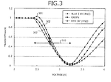
- Fig. 3 is a graph (part 1) depicting an example of the transmittance characteristics of the optical device depicted in Fig. 2 .
- the horizontal axis indicates the voltage[V] applied to the wave plate 132 implemented by a liquid crystal cell.
- the vertical axis indicates the transmittance (transmission rate) of the polarization film 210 with respect to the light output from the stacked wave plate 130.
- the transmission polarization direction 121a of the polarization film 121 for blue laser light is assumed to be tilted -10[deg] with respect to the given direction (the ordinary axis directions 131a and 133a of the wave plates 131 and 133). Further, the transmission polarization direction 122a of the polarization film 122 for green laser light is assumed to be parallel to the given direction. The transmission polarization direction 123a of the polarization film 123 for red laser light is assumed to be tilted 12[deg] with respect to the given direction. A calculation method for these tilted angles will be described hereinafter.
- Transmittance characteristics 301 are characteristics of the transmittance of the blue laser light through the polarization film 210 when voltage is applied to the wave plate 132.
- Transmittance characteristics 302 are characteristics of the transmittance of the green laser light through the polarization film 210 when voltage is applied to the wave plate 132.
- Transmittance characteristics 303 are characteristics of the transmittance of the red laser light through the polarization film 210 when voltage is applied to the wave plate 132.
- the phase difference (retardation) occurring in the polarization components at the stacked wave plate 130 changes, whereby the polarization directions 141 to 143 of the light output from the stacked wave plate 130 change. Consequently, by changing the voltage applied to the wave plate 132 and as indicated by the transmittance characteristics 301 to 303, at the polarization film 210, the transmittance of the light output from the stacked wave plate 130 can be changed. For example, by controlling the voltage applied to the wave plate 132 to be within a range 310, in which the transmitted amount of light for the transmittance characteristics 301 to 303 changes uniformly, the intensity of the output light can be controlled simply.
- the transmittance of each wavelength component changes uniformly with respect to the voltage applied to the wave plate 132.
- changes in the relative intensities of the wavelength components can be suppressed and the optical intensity of the output light can be controlled.
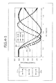
- Fig. 4-1 is a graph depicting, for reference, an example of transmittance characteristics in a case where the transmission polarization directions of the polarization films for each of the wavelengths are assumed to be identical (no tilting of the transmission polarization direction for any of the wavelengths).
- Fig. 4-1 portions identical to those depicted in Fig. 2 or Fig. 3 are given the same reference numerals used in Figs. 2 and 3 , and description thereof is omitted.
- the transmittance on the vertical axis is indicated by the electrical power[mA] of the received light in a case where the light output from the polarization film 210 is received (similarly for Figs. 4-2 to 4-4 ).
- the change in transmittance varies among the wavelength components with respect to the voltage applied to the wave plate 132. Consequently, when the optical intensity of the output light is controlled, the relative intensities of the wavelength components change.
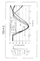
- Fig. 4-2 is a graph (part 2) depicting an example of transmittance characteristics in the optical device depicted in Fig. 2 .
- Fig. 4-2 portions identical to those depicted in Fig. 2 or Fig. 3 are given the same reference numerals used in Figs. 2 and 3 , and description thereof is omitted.
- the transmittance on the vertical axis is indicated by the electrical power[mA] of the received light in a case where the light output from the polarization film 210 is received.
- the voltage on the horizontal axis is depicted from 2[V] to 5[V].
- the transmittance of each wavelength component can be changed uniformly within the voltage range 310. Consequently, changes in the relative intensities of the wavelength components can be suppressed and the optical intensity of the output light can be controlled.
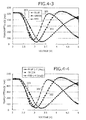
- Fig. 4-3 is a graph depicting, for reference, an example of transmittance characteristics in a case where in place of the stacked wave plate, a single liquid crystal cell is disposed and the transmission polarization directions of the polarization films are assumed to be identical.
- Fig. 4-3 portions identical to those depicted in Fig. 4-1 are given the same reference numerals used in Fig. 4-1 , and description thereof is omitted.
- the stacked wave plate 130 depicted in Fig. 2 is assumed to be replaced by a single liquid crystal cell and the transmission polarization directions 121a to 123a of the polarization films 121 to 123 are assumed to be identical (no tilting of the transmission polarization direction for any of the wavelengths).
- the change in transmittance varies among the wavelength components with respect to the voltage applied to the wave plate 132. Consequently, when the optical intensity of the output light is controlled, the relative intensities of the wavelength components change.
- Fig. 4-4 is a graph depicting, for reference, an example of transmittance characteristics in a case where in place of the stacked wave plate, a single liquid crystal cell is disposed and the transmission polarization directions of the polarization films are assumed to be staggered.
- Fig. 4-4 portions identical to those depicted in Fig. 4-1 are given the same reference numerals used in Fig. 4-1 and description thereof is omitted.
- the stacked wave plate 130 depicted in Fig. 2 is assumed to be replaced with a single liquid crystal cell and the transmission polarization directions 121a to 123a of the polarization films 121 to 123 are assumed to be staggered.
- the transmission polarization direction 121a of the polarization film 121 for blue laser light is assumed to be tilted -7[deg] with respect to the given direction.
- the transmission polarization direction 122a of the polarization film 122 for green laser light is assumed to be parallel to the given direction.
- the transmission polarization direction 123a of the polarization film 123 for red laser light is assumed to be tilted -4[deg] with respect to the given direction.
- the change in transmittance varies among the wavelength components with respect to the voltage applied to the wave plate 132. Consequently, when the optical intensity of the output light is controlled, the relative intensities of the wavelength components change.
- staggering the transmission polarization directions 121a to 123a in the optical device 100 equipped with the stacked wave plate 130 enables a uniform change to be effected in the polarization directions (transmittance) of the wavelengths with respect to the voltage applied.
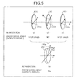
- Fig. 5 is a diagram depicting an example of operation of the stacked wave plate.
- components identical to those depicted in Fig. 1 or Fig. 2 are given the same reference numerals used in Figs. 1 and 2 , and description thereof is omitted.
- the x axis corresponds to the given direction above (0[deg]).
- the z axis corresponds to the travel direction of the light. Retardation of the wave plates 131, 133 depicted in Fig. 5 is assumed to be ⁇ 1, respectively. Further, orientation angles (azimuth angle) between the given direction in the wave plates 131 and 133 and the ordinary axis directions 131a and 133a are assumed to be ⁇ 1, respectively.
- Retardation of the wave plate 132 is assumed to be ⁇ 2; and the orientation angle between the given direction of the wave plate 132 and the ordinary axis direction 132a is assumed to be ⁇ 2.
- the direction of the ordinary axis directions 131a and 133a of the wave plates 131 and 133 is defined as a reference of 0[deg].
- the orientation angle ⁇ 1 of the wave plates 131 and 133 is 0[deg].
- the stacked wave plate 130 depicted in Fig. 5 is assumed to have the stacked wave plate 130 formed by the wave plates 131 to 133, as 1 wave plate.
- the ordinary axis direction 130a indicates the direction of an assumed ordinary axis of the stacked wave plate 130. Retardation of the stacked wave plate 130 is assumed to be ⁇ e.
- the orientation angle between the ordinary axis direction 130a of the stacked wave plate 130 and the given direction is assumed to be ⁇ e.
- the retardation ⁇ e of the stacked wave plate 130 and the orientation angle ⁇ e can be expressed as Equations (1) and (2) by a calculation based on the retardation ⁇ 1 and ⁇ 2 of the wave plates 131 to 133, the orientation angle ⁇ and Jones matrices.
- Equation (3) retardation ⁇ x of a wave plate x (the wave plates 131 to 133) changes according to the wavelength of the transmitted light as indicated by Equation (3).
- ⁇ nx is the refractive index (birefringence) of the wave plate x.
- ne is the refractive index for the direction of the extraordinary axis (fast axis) of the wave plate.
- the extraordinary axis is the axis for which the refractive index for birefringence is lowest.
- “no” is the refractive index for the direction of the ordinary axis of the wave plate.
- ⁇ nx is determined, for example, by the material of the wave plate x, the wavelength of the transmitted light, etc. The wavelength dependency of ⁇ nx will be discussed hereinafter.
- Equation (4) is satisfied.
- Equation (5) and (6) are yielded.
- the orientation angle ⁇ between the wave plate 132 and the wave plates 131 and 133 can be changed.
- the orientation angle ⁇ between the wave plate 132 and the wave plates 131 and 133 suffices to be 45[deg] or 135[deg], i.e., ⁇ /4 ⁇ (2n-1) (where, n is a natural number).
- the orientation angle ⁇ between the wave plate 132 and the wave plates 131 and 133 suffices to be 22.5[deg], 67.5[deg], 112.5[deg], or 157.5[deg], i.e., ⁇ /8 ⁇ (2n-1).
- the retardation ⁇ x of the wave plate x (the wave plates 131 to 133) is dependent on wavelength.
- an arbitrary retardation ⁇ e (e.g., ⁇ /2, ⁇ /4, etc.) can be obtained with respect to the light output from the stacked wave plate 130.
- the wave plates 131 to 133 are designed such that a desired retardation ⁇ e is induced.
- a retardation ⁇ e of ⁇ /4 is assumed to be induced.
- the wavelength (blue) of the laser light source 111 is assumed to be ⁇ B; the wavelength (green) of the laser light source 112 is assumed to be ⁇ G; and the wavelength (red) of the laser light source 113 is assumed to be ⁇ R.
- the wave plates 131 to 133 are designed such that a desirable retardation ⁇ e is induced on the light of the wavelength ⁇ G, which is an intermediate wavelength among the wavelengths ⁇ B, ⁇ G, and ⁇ R. As a result, deviation occurring at each of the wavelengths can be reduced.
- the refractive index ⁇ n also changes according to wavelength ⁇ .
- the refractive index ⁇ n is approximated by a+b/ ⁇ 2 +c/ ⁇ 4 (up to the third term). Therefore, Equation (3) can be approximated as indicated by Equation (9).
- Equation (3) can be approximated as indicated by Equation (9).
- the coefficients a, b, and c for the wave plates 131 and 133 are assumed to be a1, b1, and c1, respectively.
- the thickness d of the wave plates 131 and 133 is assumed to be d1.
- the coefficients a, b, and c for the wave plate 132 are assumed to be a2, b2, and c2, respectively.
- the thickness d of the wave plate 132 is assumed to be d2.
- Equation 10 the retardation ⁇ 1(B) of the wave plates 131 and 133 with respect to light of the wavelength ⁇ B is as expressed by Equation (10). Further, the retardation ⁇ 2(B) of the wave plate 132 with respect to light of the wavelength ⁇ B is as expressed by Equation (11).
- Equation (12) The retardation ⁇ 1(R) of the wave plates 131 and 133 with respect to light of the wavelength ⁇ R is as expressed by Equation (12).
- the retardation ⁇ 2(R) of the wave plate 132 with respect to light of the wavelength ⁇ R is as expressed by Equation (13).
- ⁇ e arccos cos 2 ⁇ ⁇ cos ⁇ ⁇ ⁇ 1 + ⁇ ⁇ 2 / 2 + sin 2 ⁇ ⁇ cos ⁇ ⁇ ⁇ 1 - ⁇ ⁇ 2 / 2 ⁇ 2
- ⁇ e arcsin sin ⁇ ⁇ 2 / 2 ⁇ sin 2 ⁇ ⁇ sin ⁇ e / 2 ⁇ 1 2
- Equations (16) and (17) are obtained.
- the orientation angle ⁇ between the wave plate 132 and the wave plates 131 and 133 is assumed to be ⁇ /8 ⁇ (2n-1). Further, to obtain a retardation ⁇ e of ⁇ /2, the orientation angle ⁇ between the wave plate 132 and the wave plates 131 and 133 is assumed to be ⁇ /4 ⁇ (2n-1).
- Fig. 6 is a graph depicting an example of characteristics of the retardation of the stacked wave plate with respect to orientation angle.
- the horizontal axis indicates the orientation angle ⁇ between the wave plate 132 and the wave plates 131 and 133.
- the vertical axis indicates the retardation ⁇ e of the stacked wave plate 130.
- Retardation characteristics 600 indicate the characteristics of the retardation ⁇ e with respect to the orientation angle ⁇ .
- the retardation ⁇ e of the stacked wave plate 130 changes between 0 and 2 ⁇ according to the orientation angle ⁇ between the wave plate 132 and the wave plates 131 and 133.
- Fig. 7-1 is a graph depicting an example of characteristics of the retardation of the stacked wave plate with respect to wavelength.
- the horizontal axis indicates the wavelength ⁇ [nm] of the light.
- the vertical axis indicates the retardation ⁇ e of the stacked wave plate 130.
- Retardation characteristics 711 are characteristics of the retardation ⁇ e with respect to the wavelength ⁇ of a single ⁇ /4 plate, which a conventional stacked structure does not have.
- Retardation characteristics 712 are characteristics of the retardation ⁇ e with respect to the wavelength ⁇ in the stacked wave plate 130, which includes the wave plates 131 to 133 and is operated as a ⁇ /4 plate.
- Retardation characteristics 713 are characteristics of ideal retardation ⁇ e and indicate constant retardation with respect to the wavelength ⁇ .
- the wave plates 131 to 133 are designed such that a desired retardation is induced on the light of the wavelength ⁇ G, even without a tilting of the transmission polarization direction 122a. Consequently, as indicated by the retardation characteristics 712, the retardation ⁇ e for about 512[nm], which corresponds to the wavelength ⁇ G, is the closest to the ideal retardation characteristics 713.
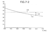
- Fig. 7-2 is a graph depicting an example of characteristics of the orientation angle of the stacked wave plate with respect to wavelength.
- the horizontal axis indicates the wavelength ⁇ [nm] of the light.
- the vertical axis indicates the orientation angle ⁇ e of the stacked wave plate 130.
- Orientation angle characteristics 721 are characteristics of the orientation angle ⁇ e of the stacked wave plate 130 with respect to wavelength ⁇ .
- Orientation angle characteristics 722 are characteristics of the ideal orientation angle ⁇ e and indicate an angle of 45[deg].
- the wave plates 131 to 133 are designed such that a desired retardation is induced on the light of the wavelength ⁇ G, even without a tilting of the transmission polarization direction 122a. Consequently, as indicated by the orientation angle characteristics 721, the orientation angle ⁇ e for about 512[nm], which corresponds to the wavelength ⁇ G, is the closest to the ideal orientation angle characteristics 722.
- the transmission polarization direction 123a corresponding to the wavelength ⁇ R is designed to be tilted -12[deg] with respect to the given direction.
- an offset of about -10[deg] is present between the orientation angle ⁇ e of the stacked wave plate 130 and the ideal orientation angle characteristics 722. Consequently, as described above, the transmission polarization direction 121a corresponding to the wavelength ⁇ B is designed to be tilted 10[deg] with respect to the given direction.
- the retardation ⁇ e when the stacked wave plate is operated as a ⁇ /4 plate as depicted in Fig. 1 covers a broad band and becomes a value close to ⁇ /2 (for example, refer to Fig. 7-1 ).
- the tilt with respect to the given direction of the transmission polarization directions 121a and 123a of the polarization films 121 and 123 for the wavelengths ⁇ B and ⁇ R, is designed based on the orientation angle ⁇ e obtained as described.
- polarization directions 141 to 143 of the emitted light are for circular polarization.
- Fig. 8-1 is a diagram (part 1) depicting an example of the ordinary axis directions and transmission polarization directions in the stacked wave plate, at the polarization films respectively corresponding to each wavelength.
- Fig. 8-1 depicts from the top, the polarization films 121 to 123 respectively corresponding to the wavelength ⁇ B, the wavelength ⁇ G, and the wavelength ⁇ R; the respective transmission polarization directions 121a, 122a, and 123a; and the ordinary axis direction 130a of the stacked wave plate 130.
- the transmission polarization direction 122a of the polarization film 122 which corresponds to the laser light of the wavelength ⁇ G is taken as a reference and is designed to be parallel to the given direction (0[deg]).
- the orientation angle ⁇ e between the given direction (0[deg]) and the ordinary axis direction 130a is 33[deg], from Fig. 7-2 .
- the transmission polarization direction 123a is tilted by the offset 723 (described in Fig. 7-2 ) of about 12[deg] occurring between the orientation angle ⁇ e of the stacked wave plate 130 and the ideal orientation angle characteristics 722.
- the transmission polarization direction 121a is designed to be tilted 10[deg] with respect to the given direction such that the difference of the ordinary axis direction 130a and the transmission polarization direction 121a of the polarization film 121, which is for the blue laser light, is 45[deg].
- Fig. 8-2 is a diagram (part 2) depicting an example of the ordinary axis directions and transmission polarization directions in the stacked wave plate, at the polarization films respectively corresponding to each the wavelength.
- Fig. 8-2 depicts from the top, similar to Fig. 8-1 , the polarization films 121 to 123 respectively corresponding to the wavelength ⁇ B, the wavelength ⁇ G, and the wavelength ⁇ R; the respective transmission polarization directions 121a, 122a, and 123a; and the ordinary axis direction 130a of the stacked wave plate 130.
- the angles between the polarization directions of the light input to the stacked wave plate 130 operated as a ⁇ /4 plate are as follows.
- the transmission polarization directions 121a to 123a are adjusted such that, of the light emitted by the laser light sources 111 to 113, the angle ⁇ ( ⁇ 1, ⁇ 2) between the polarization direction of the light of the wavelength ⁇ 1 and the polarization direction of the light of the wavelength ⁇ 2 satisfies Equations (18) and (19).
- the transmission polarization direction 121a which is the polarization direction of the blue light (wavelength 450[nm])
- the calculation is similar.
- refractive index ⁇ n1( ⁇ ) of the wave plates 131 and 133 can be approximated by a1+b1/ ⁇ 2 +c1/ ⁇ 4 +d1/ ⁇ 6 ... from the Cauchy dispersion equation. Further, the refractive index ⁇ n2( ⁇ ) of the wave plate 132 can be approximated by a2+b2/ ⁇ 2 +c2/ ⁇ 4 +d2/ ⁇ 6 ....
- the refractive index ⁇ n1( ⁇ ) of the wave plates 131 and 133 can be approximated by A1+A2/ ⁇ 2 +A3/ ⁇ 4 +A4/ ⁇ 6 ...+A(m)/ ⁇ (2(m-1)).
- the coefficients specific to the material of the wave plate 132 to be B1, B2, B3, ..., Bm
- the refractive index ⁇ n2( ⁇ ) of the wave plate 132 can be approximately by B1+B2/ ⁇ 2 +B3/ ⁇ 4 +B4/ ⁇ 6 ...+B(m)/ ⁇ (2(m-1)).
- the angles between the polarization directions of the light input to the stacked wave plate 130 operated as a ⁇ /2 plate are as follows.
- the transmission polarization directions 121a to 123a are adjusted such that, of the light emitted by the laser light sources 111 to 113, the angle ⁇ ( ⁇ 1, ⁇ 2) between the polarization direction of the light of the wavelength ⁇ 1 and the polarization direction of the light of the wavelength ⁇ 2 satisfies Equations (20) and (21).
- Equations (20) and (21) As a result, differences in the orientation angle ⁇ e occurring in the stacked wave plate 130 consequent to differences in the wavelength of the light can be corrected.
- the transmission polarization direction 121a which is the polarization direction of the blue light (wavelength 450[nm])
- the calculation is similar.
- the refractive index ⁇ n1( ⁇ ) of the wave plates 131 and 133 can be approximately by a1+b1/ ⁇ 2 +c1/ ⁇ 4 +d1/ ⁇ 6 ... from the Cauchy dispersion equation. Further, the refractive index ⁇ n2( ⁇ ) of the wave plate 132 can be approximated by a2+b2/ ⁇ 2 +c2/ ⁇ 4 +d2/ ⁇ 6 ....
- the refractive index ⁇ n1( ⁇ ) of the wave plates 131 and 133 can be approximated by A1+A2/ ⁇ 2 +A3/ ⁇ 4 +A4/ ⁇ 6 ...+A(m)/ ⁇ (2(m-1)).
- the coefficients specific to the material of the wave plate 132 to be B1, B2, B3, ..., Bm
- the refractive index ⁇ n2( ⁇ ) of the wave plate 132 can be approximately by B1+B2/ ⁇ 2 +B3/ ⁇ 4 +B4/ ⁇ 6 ...+B(m)/ ⁇ (2(m-1)).
- Fig. 9-1 is a diagram depicting a configuration example of the coupling unit.
- the coupling unit disposed in the optical device 100 for example, can be implemented by a fiber coupler 910.
- description will be given for a case where the coupling unit is disposed between the stacked wave plate 130 and the polarization films 121 to 123 (similarly with respect to Figs. 9-2 to 9-4 ).
- the fiber coupler 910 for example, includes polarization maintaining fibers 911 to 913, a combiner 914, and a polarization maintaining fiber 915.
- the polarization maintaining fibers 911 to 913, and 915 for example, are polarization maintaining fibers (PMF) that maintain the polarization state of input laser light and output the laser light.
- PMF polarization maintaining fibers
- Blue laser light (B) output from the polarization film 121 is input to the polarization maintaining fiber 911.
- the polarization maintaining fiber 911 maintains the polarization state of the input blue laser light (B) and outputs the blue laser light (B) to the combiner 914.
- Green laser light (G) output from the polarization film 122 is input to the polarization maintaining fiber 912.
- the polarization maintaining fiber 912 maintains the polarization state of the green laser light (G) and outputs the green laser light (G) to the combiner 914.
- Red laser light (R) output from the polarization film 123 is input to the polarization maintaining fiber 913.
- the polarization maintaining fiber 913 maintains the polarization state of the red laser light (R) and outputs the red laser light (R) to the combiner 914.
- the combiner 914 is a multiplexer that multiplexes the laser light output from the polarization maintaining fibers 911 to 913.
- the combiner 914 outputs the multiplexed laser light to the polarization maintaining fiber 915.
- the polarization maintaining fiber 915 maintains the polarization state of the laser light output from the combiner 914 and outputs the laser light.
- the laser light output from the polarization maintaining fiber 915 is laser light that includes red, green, and blue light. Further, the laser light output from the polarization maintaining fiber 915 is input to the stacked wave plate 130.
- the laser light output from the polarization films 121 to 123 can be multiplexed with the respective polarization directions maintained, and output to the stacked wave plate 130 by the fiber coupler 910 depicted in Fig. 9-1 .
- Fig. 9-2 is a diagram depicting a first modification example of the coupling unit.
- the coupling unit disposed in the optical device 100 can be implemented by a coupling unit 920 that uses a dichroic mirror.
- the coupling unit 920 may include a mirror 921, and dichroic mirrors 922 and 923.
- the mirror 921 reflects and outputs to the dichroic mirror 922, the red laser light (R) output from the polarization film 123.
- the dichroic mirror 922 reflects and outputs to the dichroic mirror 923, the green laser light (G) output from the polarization film 122. Further, the dichroic mirror 922 transmits and outputs to the dichroic mirror 923, the red laser light (R) output from the mirror 921.
- the dichroic mirror 923 reflects and outputs downstream, the blue laser light (B) output from the polarization film 121.
- the dichroic mirror 923 further transmits and outputs downstream, the red laser light (R) and the green laser light (G) output from the dichroic mirror 922.
- the dichroic mirrors 922 and 923 can each be implemented by, for example, dielectric multilayers.
- the laser light output from the dichroic mirror 923 is laser light that includes red, green, and blue light. Further, the laser light output from the dichroic mirror 923 is input to the stacked wave plate 130.
- the laser light output from the polarization films 121 to 123 can be multiplexed with the respective polarization directions maintained, and output to the stacked wave plate 130 by the coupling unit 920 that is depicted in Fig. 9-2 and uses a dichroic mirror.
- Fig. 9-3 is a diagram depicting a second modification example of the coupling unit.
- portions identical to those depicted in Fig. 9-2 are given the same reference numerals used in Fig. 9-2 and description thereof is omitted.
- the coupling unit 920 that uses a dichroic mirror may be configured to omit the mirror 921 in the configuration depicted in Fig. 9-2 .
- the dichroic mirror 922 reflects and outputs to the dichroic mirror 923, the red laser light (R) output from the polarization film 123.
- the dichroic mirror 922 further transmits and outputs to the dichroic mirror 923, the green laser light (G) output from the polarization film 122.
- the red laser light (R) output from the polarization film 123 and the green laser light (G) output from the polarization film 122 is input to the dichroic mirror 922, whereby the mirror 921 depicted in Fig. 9-2 may be omitted.
- Fig. 9-4 is a diagram depicting a third modification example of the coupling unit.
- the coupling unit disposed in the optical device 100 may be implemented by a holographic coupler 940.
- the holographic coupler 940 is a volume hologram recorded such that the diffraction angle differs according to wavelength.
- the laser light output from the polarization films 121 to 123 collects at the holographic coupler 940 and when being transmitted by the holographic coupler 940, is output in the same direction by diffraction of an angle that corresponds to wavelength.
- the laser light output from the polarization films 121 to 123 can be multiplexed with the respective polarization directions maintained, and output to the stacked wave plate 130 by the holographic coupler 940 depicted in Fig. 9-4 .
- deviation of the polarization directions of the wavelength components can be suppressed. Further, for example, increases in apparatus size can be suppressed as compared to a configuration that disposes multiple wave plates optimized for each wavelength component, to obtain a given retardation for each the wavelength component.
- the laser light sources 111 to 113 have been given as one example of the light sources, the light sources are not limited to the laser light sources 111 to 113, and for example, may be 2, or 4 or more light sources, each emitting laser light of a different wavelength. Further, the wavelength of the laser light is not limited to 450[nm] (blue), 512[nm] (green), and 650[nm] (red) and an arbitrary wavelength may be used.
- the angles of the laser light sources may be adjusted such that the transmission polarization directions 121a, 122a, and 123a substantially coincide.
- optical loss at the polarization films 121 to 123 can be suppressed.
- a configuration that omits the polarization films 121 to 123 is possible.
- a member that adjusts the angle of the laser light sources 111 to 113 is the polarization adjusting unit that adjusts the polarization directions of the light.
- optical device 100 has a function of an attenuator
- apparatuses to which the optical device 100 can be applied are not limited hereto.
- the optical device 100 depicted in Fig. 1 can be applied to a projector and the like.
- the optical device according to the present invention is useful for an optical device that outputs light of multiple wavelengths, in a given polarization direction; and is particularly suitable for an attenuator and the like that change optical intensity according to polarization direction.
- the attenuator for example, can be used in a head-up display in a vehicle, aircraft, etc., and is useful for changing the brightness of display, according to the brightness of the environment while driving/flying.
- the use of an attenuator based on the present invention enables faster adjustment of the overall amount of light, with the color tone as is.
- the attenuator can be used commonly for multiple light source wavelengths, thereby enabling reductions in size.
- the stacked wave plate When the optical device is used as an attenuator, the stacked wave plate is operated as a ⁇ /2 plate and the linear polarization output when voltage is applied is designed to be orthogonal to the polarization film, thereby enabling a dark state to be obtained. In this dark state, the output polarization direction differs according to wavelength and therefore, hue can be adjusted by adjusting the light source intensity.
Landscapes
- Physics & Mathematics (AREA)
- Nonlinear Science (AREA)
- General Physics & Mathematics (AREA)
- Optics & Photonics (AREA)
- Chemical & Material Sciences (AREA)
- Crystallography & Structural Chemistry (AREA)
- Engineering & Computer Science (AREA)
- General Engineering & Computer Science (AREA)
- Mathematical Physics (AREA)
- Polarising Elements (AREA)
- Liquid Crystal (AREA)
Abstract
Description
- The present invention relates to an optical device configured to output light for which the direction of polarization has been adjusted.
- It is known that a conventional wave plate induces a given phase difference (retardation) to polarization components of light emitted from an optical source such as a laser light source and thereby, adjusts the polarization direction of the light emitted from the optical source to output light for which the polarization direction is controlled. Wave plates include, for example, λ/2 wave plates that induce a phase difference of λ/2 (where, λ is the wavelength of the light) on polarization components and λ/4 wave plates that induce a phase difference of λ/4 on polarization components. A wave plate, for example, that uses polarization film to transmit light of an amount that corresponds to the polarization direction is employed in an attenuator. Further, to implement a broadband wave plate, a stacked wave plate is known that is a combination of plural wave plates (for example, refer to
Patent Documents -
- Patent Document 1: Japanese Patent Application Laid-Open Publication No.
2008-070690 - Patent Document 2: Published Japanese-Translation of
PCT Application, Publication No. 2003/091768 - Nonetheless, with the conventional technologies above, when light that includes plural wavelength components is input to the stacked wave plate, a problem arises in that the polarization direction of the light output from the stacked wave plate deviates according to wavelength component. Consequently, for example, a problem arises in that at an attenuator that uses a stacked wave plate and polarization film, the amount of attenuation of the output light deviates according to wavelength component (optical color).
- To solve the problems of the conventional technologies, an object of the present invention is to provide an optical device that suppresses deviation of the polarization direction, occurring for each wavelength component.
- To solve the problems above and achieve an object, one aspect of an optical device according to the present invention includes light sources that respectively emit light of a different wavelength; a stacked wave plate that includes wave plates that transmit the light emitted by the light sources and are disposed in series, and induces a phase difference on polarization components of the light transmitted by the wave plates; and a polarization adjusting unit that adjusts polarization directions of the light such that an angle between the polarization directions of the light emitted by the light sources and input to the stacked wave plate becomes an angle that corrects an orientation angle difference that occurs at the stacked wave plate and is caused by differences in the wavelengths of the light.
- In this manner, by preliminarily adjusting the polarization directions of the light according to wavelength, differences in the retardation of the stacked wave plate consequent to the differences in the wavelengths of the light are corrected and deviation of the polarization directions of each wavelength component of the output light can be suppressed.
- According to the present invention, an effect of suppressing deviation of the polarization directions of each wavelength component is achieved.
-
-
Fig. 1 is a diagram depicting an example of a configuration of an optical device according to an embodiment; -
Fig. 2 is a diagram depicting an example of a modification of the optical device; -
Fig. 3 is a graph (part 1) depicting an example of transmittance characteristics of the optical device depicted inFig. 2 ; -
Fig. 4-1 is a graph depicting, for reference, an example of transmittance characteristics in a case where transmission polarization directions of polarization films for each wavelength are assumed to be identical (no tilting of the transmission polarization direction for any wavelength); -
Fig. 4-2 is a graph (part 2) depicting an example of transmittance characteristics in the optical device depicted inFig. 2 ; -
Fig. 4-3 is a graph depicting, for reference, an example of transmittance characteristics in a case where in place of a stacked wave plate, a single liquid crystal cell is disposed and the transmission polarization directions of the polarization films are assumed to be identical; -
Fig. 4-4 is a graph depicting, for reference, an example of transmittance characteristics in a case where in place of the stacked wave plate, a single liquid crystal cell is disposed and the transmission polarization directions of the polarization films are assumed to be staggered; -
Fig. 5 is a diagram depicting an example of operation of the stacked wave plate; -
Fig. 6 is a graph depicting an example of characteristics of retardation of the stacked wave plate with respect to orientation angle; -
Fig. 7-1 is a graph depicting an example of characteristics of the retardation of the stacked wave plate with respect to wavelength; -
Fig. 7-2 is a graph depicting an example of characteristics of the orientation angle of the stacked wave plate with respect to wavelength; -
Fig. 8-1 is a diagram (part 1) depicting an example of ordinary axis directions and transmission polarization directions in the stacked wave plate, at the polarization films respectively corresponding to each wavelength; -
Fig. 8-2 is a diagram (part 2) depicting an example of the ordinary axis directions and transmission polarization directions in the stacked wave plate, at the polarization films respectively corresponding to each the wavelength; -
Fig. 9-1 is a diagram depicting a configuration example of a coupling unit; -
Fig. 9-2 is a diagram depicting a first modification example of the coupling unit; -
Fig. 9-3 is a diagram depicting a second modification example of the coupling unit; and -
Fig. 9-4 is a diagram depicting a third modification example of the coupling unit. - An embodiment of an optical device according to the present invention will be described in detail with reference to the accompanying drawings.
-
Fig. 1 is a diagram depicting an example of a configuration of the optical device according to the embodiment. As depicted inFig. 1 , anoptical device 100 includeslaser light sources 111 to 113,polarization films 121 to 123, and astacked wave plate 130. Theoptical device 100 is an optical device that induces a given phase difference on polarization components of the laser light emitted by thelaser light sources 111 to 113 and thereby, adjusts the polarization direction of the laser light to output light for which the polarization direction has been controlled. - The
laser light sources 111 to 113 respectively output laser light of a different wavelength. For example, thelaser light source 111 outputs blue (wavelength 450[nm]) laser light. Thelaser light source 112 outputs green (wavelength 512[nm]) laser light. Thelaser light source 113 outputs red (wavelength 650[nm]) laser light. - The laser light output from the
laser light sources 111 to 113 is input to thepolarization films 121 to 123, respectively. Each of thelaser light sources 111 to 113, for example, may be a laser apparatus that directly outputs laser light of each wavelength, or may be a second harmonic generation (SHG) laser apparatus. - The
polarization films 121 to 123 are a polarization adjusting unit that adjusts the polarization directions of the light such that angles between the polarization directions of the light output by thelaser light sources 111 to 113 and input to thestacked wave plate 130 becomes a given angle. The given angle is an angle that corrects orientation angle differences that occur in thestacked wave plate 130 consequent to the differences in optical wavelength (described hereinafter). - The
polarization film 121 is a polarizer that, of the laser light emitted by thelaser light source 111, transmits and outputs to thestacked wave plate 130, only a linear polarization component of atransmission polarization direction 121a. Thepolarization film 122 is a polarizer that, of the laser light emitted by thelaser light source 112, transmits and outputs to thestacked wave plate 130, only a linear polarization component of atransmission polarization direction 122a. - The
polarization film 123 is a polarizer that, of the laser light emitted by thelaser light source 113, transmits and outputs to thestacked wave plate 130, only a linear polarization component of atransmission polarization direction 123a. Thetransmission polarization directions polarization films 121 to 123 are designed to be directions that respectively differ according to the wavelength of thelaser light sources 111 to 113. Thetransmission polarization directions - If the
laser light sources 111 to 113 emit linearly polarized laser light, the angles of thelaser light sources 111 to 113 may be adjusted such that the polarization directions of the laser light from thelaser light sources 111 to 113 substantially coincide with thetransmission polarization directions polarization films 121 to 123 can be suppressed. Further, in this case, the configuration can omit thepolarization films 121 to 123. In such a case, a member that adjusts the angles of thelaser light sources 111 to 113 is the polarization adjusting unit, which adjusts the polarization directions of the light. - The
stacked wave plate 130 is operated as a wave plate that induces a given phase difference (retardation) on orthogonal polarization components of the light emitted from thelaser light sources 111 to 113 and transmitted by thepolarization films 121 to 123. For example, thestacked wave plate 130 is operated as a λ/4 plate that induces a λ/4 phase difference (where, λ is optical wavelength) on the polarization components of the light from thepolarization films 121 to 123, or as a λ/2 plate that induces a λ/2 phase difference on the polarization components of the light from thepolarization films 121 to 123. - The
stacked wave plate 130 includeswave plates 131 to 133 that are disposed in series. Each of thewave plates 131 to 133 is a birefringent element that causes a given phase difference between orthogonal polarization components of the transmitted light. Thewave plate 131 is a first wave plate that transmits to thewave plate 132, the light output from thepolarization films 121 to 123. Thewave plate 132 is a second wave plate that transmits to thewave plate 133, the light output from thewave plate 131. Thewave plate 133 is a third wave plate that transmits downstream, the light output from thewave plate 132. For example, thewave plates wave plate 132 is a λ/2 plate. -
Ordinary axis directions wave plates 131 to 133, respectively. The ordinary axis (slow axis) is the axis for which the refractive index for birefringence is highest in the wave plate. In the example depicted inFig. 1 , theordinary axis directions wave plate 130 as a λ/4 plate. More specifically, theordinary axis directions ordinary axis direction 132a is set to a direction different from theordinary axis directions -
Polarization directions 141 to 143 indicate polarization directions of the respective wavelength components: blue, green, and red, in the light output from the stackedwave plate 130. Since theordinary axis directions wave plate 130 as a λ/4 plate, thepolarization directions 141 to 143 are for circular polarization. - Downstream to the
polarization films 121 to 123, a coupling unit may be disposed that maintains at the respective polarization directions, the light output from thepolarization films 121 to 123 and that couples the light. The coupling unit, for example, can be disposed between the stackedwave plate 130 and thepolarization films 121 to 123, or downstream to the stackedwave plate 130. An example of a configuration of the coupling unit will be described hereinafter (for example, refer toFigs. 9-1 to Fig. 9-4 ). -
Fig. 2 is a diagram depicting an example of a modification of the optical device. InFig. 2 , components identical to those depicted inFig. 1 are given the same reference numerals used inFig. 1 and description thereof is omitted. As depicted inFig. 2 , downstream to the stackedwave plate 130 depicted inFig. 1 , apolarization film 210 is disposed, thereby enabling theoptical device 100 to have a function of an attenuator. - In this case, for example, the
ordinary axis directions wave plates 131 to 133 are designed for operating the stackedwave plate 130 as a λ/2 plate. As a result, thepolarization directions 141 to 143 of the wavelength components in the light output from the stackedwave plate 130 are respectively for linear polarization. - Further, for example, the
wave plate 132 is implemented by a liquid crystal cell. The liquid crystal cell changes the director orientation according to the voltage applied, whereby the phase difference induced on the polarization components of the transmitted light changes. As a result, by changing the voltage applied to thewave plate 132, thepolarization directions 141 to 143 of the wavelength components in the light output from the stackedwave plate 130 can be changed. - The
polarization film 210 is a polarizer that, of the light output from the stackedwave plate 130, transmits downstream, only a linear polarization component (given polarization component) of apolarization direction 211. As a result, by changing thepolarization directions 141 to 143 by changing the voltage applied to thewave plate 132, the intensity of the light transmitted through thepolarization film 210 can be changed. - Nematic liquid crystal, for example, can be used in the liquid crystal cell applied to the
wave plate 132. Further, ferroelectric liquid crystal (FLC) can be used in the liquid crystal cell applied to thewave plate 132. As a result, control of the polarization direction can be performed at high-speed. - In the
optical device 100 depicted inFig. 2 , for example, a coupling unit (for example, refer toFigs. 9-1 to 9-4 ) can be disposed between the stackedwave plate 130 and thepolarization films 121 to 123, or between the stackedwave plate 130 and thepolarization film 210, or downstream from thepolarization film 210. -
Fig. 3 is a graph (part 1) depicting an example of the transmittance characteristics of the optical device depicted inFig. 2 . InFig. 3 , the horizontal axis indicates the voltage[V] applied to thewave plate 132 implemented by a liquid crystal cell. The vertical axis indicates the transmittance (transmission rate) of thepolarization film 210 with respect to the light output from the stackedwave plate 130. - In the example depicted in
Fig. 3 , in theoptical device 100 depicted inFig. 2 , thetransmission polarization direction 121a of thepolarization film 121 for blue laser light is assumed to be tilted -10[deg] with respect to the given direction (theordinary axis directions wave plates 131 and 133). Further, thetransmission polarization direction 122a of thepolarization film 122 for green laser light is assumed to be parallel to the given direction. Thetransmission polarization direction 123a of thepolarization film 123 for red laser light is assumed to be tilted 12[deg] with respect to the given direction. A calculation method for these tilted angles will be described hereinafter. -
Transmittance characteristics 301 are characteristics of the transmittance of the blue laser light through thepolarization film 210 when voltage is applied to thewave plate 132.Transmittance characteristics 302 are characteristics of the transmittance of the green laser light through thepolarization film 210 when voltage is applied to thewave plate 132.Transmittance characteristics 303 are characteristics of the transmittance of the red laser light through thepolarization film 210 when voltage is applied to thewave plate 132. - By changing the voltage applied to the
wave plate 132, the phase difference (retardation) occurring in the polarization components at the stackedwave plate 130 changes, whereby thepolarization directions 141 to 143 of the light output from the stackedwave plate 130 change. Consequently, by changing the voltage applied to thewave plate 132 and as indicated by thetransmittance characteristics 301 to 303, at thepolarization film 210, the transmittance of the light output from the stackedwave plate 130 can be changed. For example, by controlling the voltage applied to thewave plate 132 to be within arange 310, in which the transmitted amount of light for thetransmittance characteristics 301 to 303 changes uniformly, the intensity of the output light can be controlled simply. - Further, according to the
optical device 100, by an adjustment of thetransmission polarization directions 121a to 123a of thepolarization films 121 to 123, as indicated by thetransmittance characteristics 301 to 303, the transmittance of each wavelength component changes uniformly with respect to the voltage applied to thewave plate 132. As a result, changes in the relative intensities of the wavelength components can be suppressed and the optical intensity of the output light can be controlled. -
Fig. 4-1 is a graph depicting, for reference, an example of transmittance characteristics in a case where the transmission polarization directions of the polarization films for each of the wavelengths are assumed to be identical (no tilting of the transmission polarization direction for any of the wavelengths). InFig. 4-1 , portions identical to those depicted inFig. 2 orFig. 3 are given the same reference numerals used inFigs. 2 and3 , and description thereof is omitted. InFig. 4-1 , the transmittance on the vertical axis is indicated by the electrical power[mA] of the received light in a case where the light output from thepolarization film 210 is received (similarly forFigs. 4-2 to 4-4 ). - Assuming the
transmission polarization directions 121a to 123a of thepolarization films 121 to 123 are identical, as indicated by thetransmittance characteristics 301 to 303 depicted inFig. 4-1 , the change in transmittance varies among the wavelength components with respect to the voltage applied to thewave plate 132. Consequently, when the optical intensity of the output light is controlled, the relative intensities of the wavelength components change. - For example, when light for which color has been adjusted by the relative intensities of the light output from the
laser light sources 111 to 113 is to be output from theoptical device 100, if the relative intensities of the wavelengths change at the stackedwave plate 130, light of an unintended color is output from theoptical device 100. -
Fig. 4-2 is a graph (part 2) depicting an example of transmittance characteristics in the optical device depicted inFig. 2 . InFig. 4-2 , portions identical to those depicted inFig. 2 orFig. 3 are given the same reference numerals used inFigs. 2 and3 , and description thereof is omitted. InFig. 4-2 , under the same conditions as in the example depicted inFig. 3 , the transmittance on the vertical axis is indicated by the electrical power[mA] of the received light in a case where the light output from thepolarization film 210 is received. InFig. 4-2 , similar toFig. 4-1 , the voltage on the horizontal axis is depicted from 2[V] to 5[V]. - As indicated by the
transmittance characteristics 301 to 303 depicted inFig. 4-2 , according to theoptical device 100 that staggers thetransmission polarization directions 121a to 123a of thepolarization films 121 to 123, for example, the transmittance of each wavelength component can be changed uniformly within thevoltage range 310. Consequently, changes in the relative intensities of the wavelength components can be suppressed and the optical intensity of the output light can be controlled. - For example, when light for which color has been adjusted by the relative intensities of the light respectively emitted from the
laser light sources 111 to 113 is to be output from theoptical device 100, changes in the relative intensities of the wavelength components can be suppressed. As a result, light of an intended color can be output. -
Fig. 4-3 is a graph depicting, for reference, an example of transmittance characteristics in a case where in place of the stacked wave plate, a single liquid crystal cell is disposed and the transmission polarization directions of the polarization films are assumed to be identical. InFig. 4-3 , portions identical to those depicted inFig. 4-1 are given the same reference numerals used inFig. 4-1 , and description thereof is omitted. The stackedwave plate 130 depicted inFig. 2 is assumed to be replaced by a single liquid crystal cell and thetransmission polarization directions 121a to 123a of thepolarization films 121 to 123 are assumed to be identical (no tilting of the transmission polarization direction for any of the wavelengths). - In this case, as indicated by the
transmittance characteristics 301 to 303 depicted inFig. 4-3 , the change in transmittance varies among the wavelength components with respect to the voltage applied to thewave plate 132. Consequently, when the optical intensity of the output light is controlled, the relative intensities of the wavelength components change. -
Fig. 4-4 is a graph depicting, for reference, an example of transmittance characteristics in a case where in place of the stacked wave plate, a single liquid crystal cell is disposed and the transmission polarization directions of the polarization films are assumed to be staggered. InFig. 4-4 , portions identical to those depicted inFig. 4-1 are given the same reference numerals used inFig. 4-1 and description thereof is omitted. The stackedwave plate 130 depicted inFig. 2 is assumed to be replaced with a single liquid crystal cell and thetransmission polarization directions 121a to 123a of thepolarization films 121 to 123 are assumed to be staggered. - More specifically, the
transmission polarization direction 121a of thepolarization film 121 for blue laser light is assumed to be tilted -7[deg] with respect to the given direction. Further, thetransmission polarization direction 122a of thepolarization film 122 for green laser light is assumed to be parallel to the given direction. Thetransmission polarization direction 123a of thepolarization film 123 for red laser light is assumed to be tilted -4[deg] with respect to the given direction. In this case as well, as indicated by thetransmittance characteristics 301 to 303 depicted inFig. 4-4 , the change in transmittance varies among the wavelength components with respect to the voltage applied to thewave plate 132. Consequently, when the optical intensity of the output light is controlled, the relative intensities of the wavelength components change. - As depicted in
Figs. 4-1 to 4-4 , staggering thetransmission polarization directions 121a to 123a in theoptical device 100 equipped with the stackedwave plate 130, enables a uniform change to be effected in the polarization directions (transmittance) of the wavelengths with respect to the voltage applied. -
Fig. 5 is a diagram depicting an example of operation of the stacked wave plate. InFig. 5 , components identical to those depicted inFig. 1 or Fig. 2 are given the same reference numerals used inFigs. 1 and 2 , and description thereof is omitted. InFig. 5 , the x axis corresponds to the given direction above (0[deg]). The z axis corresponds to the travel direction of the light. Retardation of thewave plates Fig. 5 is assumed to be γ1, respectively. Further, orientation angles (azimuth angle) between the given direction in thewave plates ordinary axis directions - Retardation of the
wave plate 132 is assumed to be γ2; and the orientation angle between the given direction of thewave plate 132 and theordinary axis direction 132a is assumed to be Ψ2. Here, the direction of theordinary axis directions wave plates wave plates wave plate 132 and thewave plates - The stacked
wave plate 130 depicted inFig. 5 is assumed to have the stackedwave plate 130 formed by thewave plates 131 to 133, as 1 wave plate. Theordinary axis direction 130a indicates the direction of an assumed ordinary axis of the stackedwave plate 130. Retardation of the stackedwave plate 130 is assumed to be Γe. The orientation angle between theordinary axis direction 130a of the stackedwave plate 130 and the given direction is assumed to be Ψe. - The retardation Γe of the stacked
wave plate 130 and the orientation angle Γe can be expressed as Equations (1) and (2) by a calculation based on the retardation γ1 and γ2 of thewave plates 131 to 133, the orientation angle Ψ and Jones matrices.

- In Equations (1) and (2), retardation γx of a wave plate x (the
wave plates 131 to 133) changes according to the wavelength of the transmitted light as indicated by Equation (3). In Equation (3), Δnx is the refractive index (birefringence) of the wave plate x. Typically, the refractive index n of a wave plate is n=ne-no. "ne" is the refractive index for the direction of the extraordinary axis (fast axis) of the wave plate. The extraordinary axis is the axis for which the refractive index for birefringence is lowest. "no" is the refractive index for the direction of the ordinary axis of the wave plate. "Δnx" is determined, for example, by the material of the wave plate x, the wavelength of the transmitted light, etc. The wavelength dependency of Δnx will be discussed hereinafter. "dx" is the thickness of the wave plate x.
- To use the stacked
wave plate 130 over a broad band, since it is sufficient for the retardation Γe of the stackedwave plate 130 to not be affected by refractive index changes consequent to wavelength differences of the wave plate x, the retardation Γe satisfies, for example, Equation (4).
- For example, when γ1=π/2 or γ1=3π/2, and γ2=π are satisfied, irrespective of the orientation angle Ψ between the
wave plate 132 and thewave plates 

- Therefore, by changing the orientation angle Ψ between the
wave plate 132 and thewave plates wave plate 130 is used as a λ/2 plate, the retardation suffices to be Γe=π×(2n-1). To this end, the orientation angle Ψ between thewave plate 132 and thewave plates - Further, when the stacked
wave plate 130 is used as a λ/4, the retardation suffices to be Γe=π/2×(2n-1). To this end, the orientation angle Ψ between thewave plate 132 and thewave plates - Nonetheless, as described, the retardation γx of the wave plate x (the
wave plates 131 to 133) is dependent on wavelength. In this regard, as described, by stacking the wave plates, even if the retardation γx of thewave plates 131 to 133 is dependent on wavelength, an arbitrary retardation Γe (e.g., λ/2, λ/4, etc.) can be obtained with respect to the light output from the stackedwave plate 130. - First, with respect to the light emitted from one of the
laser light sources 111 to 113, thewave plates 131 to 133 are designed such that a desired retardation Γe is induced. Here, a retardation Γe of λ/4 is assumed to be induced. Further, the wavelength (blue) of thelaser light source 111 is assumed to be λB; the wavelength (green) of thelaser light source 112 is assumed to be λG; and the wavelength (red) of thelaser light source 113 is assumed to be λR. For example, thewave plates 131 to 133 are designed such that a desirable retardation Γe is induced on the light of the wavelength λG, which is an intermediate wavelength among the wavelengths λB, λG, and λR. As a result, deviation occurring at each of the wavelengths can be reduced. - To induce a desirable retardation Γe on the light of the wavelength λG, the
wave plates 131 to 133 are designed such that γ1=π/2 or 3π/2, and γ2=π are satisfied. More specifically, for thewave plates wave plates 
- Further, for the
wave plate 132, the refractive index Δn and the thickness d are designed such that the conditions of Equation (8), which is derived from Equation (3), λ=λG, and γ=π are satisfied; where, γ2(G) is the retardation for the light of the wavelength λG at thewave plate 132.
- In Equations (7) and (8), the refractive index Δn also changes according to wavelength λ. For example, the refractive index Δn can be approximated by Δn=a+b/λ2+c/λ4+d/λ6... from the Cauchy dispersion equation; where, a, b, c, d, ... are coefficients specific to the material of the wave plate. In the description hereinafter, for example, the refractive index Δn is approximated by a+b/λ2+c/λ4 (up to the third term). Therefore, Equation (3) can be approximated as indicated by Equation (9).

- Here, the coefficients a, b, and c for the
wave plates wave plates wave plate 132 are assumed to be a2, b2, and c2, respectively. The thickness d of thewave plate 132 is assumed to be d2. - In this case, the retardation γ1(B) of the
wave plates wave plate 132 with respect to light of the wavelength λB is as expressed by Equation (11).

- The retardation γ1(R) of the
wave plates wave plate 132 with respect to light of the wavelength λR is as expressed by Equation (13).

- Here, transformation of Equations (1) and (2) yields Equations (14) and (15).


- By substituting into Equations (14) and (15), γ1 and γ2 from Equations (10) to (13), Equations (16) and (17) are obtained.


- As described, to obtain a retardation Γe of λ/4, the orientation angle Ψ between the
wave plate 132 and thewave plates wave plate 132 and thewave plates wave plate 130 for the wavelength λB or the wavelength λR are obtained. -
Fig. 6 is a graph depicting an example of characteristics of the retardation of the stacked wave plate with respect to orientation angle. InFig. 6 , the horizontal axis indicates the orientation angle Ψ between thewave plate 132 and thewave plates wave plate 130.Retardation characteristics 600 indicate the characteristics of the retardation Γe with respect to the orientation angle Ψ. As indicated by theretardation characteristics 600, the retardation Γe of the stackedwave plate 130 changes between 0 and 2π according to the orientation angle Ψ between thewave plate 132 and thewave plates -
Fig. 7-1 is a graph depicting an example of characteristics of the retardation of the stacked wave plate with respect to wavelength. InFig. 7-1 , the horizontal axis indicates the wavelength λ[nm] of the light. The vertical axis indicates the retardation Γe of the stackedwave plate 130.Retardation characteristics 711 are characteristics of the retardation Γe with respect to the wavelength λ of a single λ/4 plate, which a conventional stacked structure does not have. -
Retardation characteristics 712 are characteristics of the retardation Γe with respect to the wavelength λ in the stackedwave plate 130, which includes thewave plates 131 to 133 and is operated as a λ/4 plate.Retardation characteristics 713 are characteristics of ideal retardation Γe and indicate constant retardation with respect to the wavelength λ. - In the example depicted in
Fig. 7-1 , as described above, thewave plates 131 to 133 are designed such that a desired retardation is induced on the light of the wavelength λG, even without a tilting of thetransmission polarization direction 122a. Consequently, as indicated by theretardation characteristics 712, the retardation Γe for about 512[nm], which corresponds to the wavelength λG, is the closest to theideal retardation characteristics 713. -
Fig. 7-2 is a graph depicting an example of characteristics of the orientation angle of the stacked wave plate with respect to wavelength. InFig. 7-2 , the horizontal axis indicates the wavelength λ[nm] of the light. The vertical axis indicates the orientation angle Ψe of the stackedwave plate 130.Orientation angle characteristics 721 are characteristics of the orientation angle Ψe of the stackedwave plate 130 with respect to wavelength λ.Orientation angle characteristics 722 are characteristics of the ideal orientation angle Ψe and indicate an angle of 45[deg]. - As described, the
wave plates 131 to 133 are designed such that a desired retardation is induced on the light of the wavelength λG, even without a tilting of thetransmission polarization direction 122a. Consequently, as indicated by theorientation angle characteristics 721, the orientation angle Ψe for about 512[nm], which corresponds to the wavelength λG, is the closest to the idealorientation angle characteristics 722. - In this regard, for example, near 650[nm], which corresponds to the wavelength λR, an offset 723 of about 12[deg] is present between the orientation angle Ψe of the stacked
wave plate 130 and the idealorientation angle characteristics 722. Consequently, as described above, thetransmission polarization direction 123a corresponding to the wavelength λR is designed to be tilted -12[deg] with respect to the given direction. Further, near 450[nm], which corresponds to the wavelength λB, an offset of about -10[deg] is present between the orientation angle Ψe of the stackedwave plate 130 and the idealorientation angle characteristics 722. Consequently, as described above, thetransmission polarization direction 121a corresponding to the wavelength λB is designed to be tilted 10[deg] with respect to the given direction. - The retardation Γe when the stacked wave plate is operated as a λ/4 plate as depicted in
Fig. 1 covers a broad band and becomes a value close to π/2 (for example, refer toFig. 7-1 ). The tilt with respect to the given direction of thetransmission polarization directions polarization films - For example, as depicted in
Fig. 1 , a case will be described where thepolarization directions 141 to 143 of the emitted light are for circular polarization. -
Fig. 8-1 is a diagram (part 1) depicting an example of the ordinary axis directions and transmission polarization directions in the stacked wave plate, at the polarization films respectively corresponding to each wavelength.Fig. 8-1 depicts from the top, thepolarization films 121 to 123 respectively corresponding to the wavelength λB, the wavelength λG, and the wavelength λR; the respectivetransmission polarization directions ordinary axis direction 130a of the stackedwave plate 130. - As depicted in
Fig. 8-1 , thetransmission polarization direction 122a of thepolarization film 122, which corresponds to the laser light of the wavelength λG is taken as a reference and is designed to be parallel to the given direction (0[deg]). For the wavelength λR (650[nm]), the orientation angle Ψe between the given direction (0[deg]) and theordinary axis direction 130a is 33[deg], fromFig. 7-2 . To convert linear polarization to circular polarization, the ordinary axis of a λ/4 plate has to be 45[deg] with respect to the input linear polarization direction and therefore, in this case, thetransmission polarization direction 123a is designed to be tilted -12(=33-45)[deg] with respect to the given direction such that the difference of thetransmission polarization direction 123a of thepolarization film 123, which is for the red laser light, and theordinary axis direction 130a is 45[deg]. In other words, thetransmission polarization direction 123a is tilted by the offset 723 (described inFig. 7-2 ) of about 12[deg] occurring between the orientation angle Ψe of the stackedwave plate 130 and the idealorientation angle characteristics 722. - Similarly, for the wavelength λB (450[nm]), assuming that the orientation angle Ψe=55[deg], from
Fig. 7-2 , thetransmission polarization direction 121a is designed to be tilted 10[deg] with respect to the given direction such that the difference of theordinary axis direction 130a and thetransmission polarization direction 121a of thepolarization film 121, which is for the blue laser light, is 45[deg]. - On the other hand, when the stacked wave plate is operated as a λ/2 plate as depicted in
Fig. 2 , linear polarization that is rotated by the angle formed by the input linear polarization direction and the ordinary axis of the λ/2 plate and linear polarization that is rotated by twice this angle are transmitted. Next, as depicted inFig. 2 , a case where thepolarization directions 141 to 143 of the output wavelengths are aligned in a 90[deg] direction will be described. -
Fig. 8-2 is a diagram (part 2) depicting an example of the ordinary axis directions and transmission polarization directions in the stacked wave plate, at the polarization films respectively corresponding to each the wavelength.Fig. 8-2 depicts from the top, similar toFig. 8-1 , thepolarization films 121 to 123 respectively corresponding to the wavelength λB, the wavelength λG, and the wavelength λR; the respectivetransmission polarization directions ordinary axis direction 130a of the stackedwave plate 130. - Similar to
Fig. 8-1 , assuming that for the wavelength λG, the orientation angle Ψe=45[deg] and for the wavelength λR, the orientation angle Ψe=33[deg], thetransmission polarization direction 122a of thepolarization film 122 that corresponds to the laser light of the wavelength λG is designed to be 0[deg]; and thetransmission polarization direction 123a of thepolarization film 123 that corresponds to the laser light of the wavelength λR is arranged such that when rotated an angle that is twice the angle formed with the ordinary axis (=orientation angle Ψe), the angle is in the 90[deg] direction. In other words, thetransmission polarization direction 123a is arranged such that the angle formed by thetransmission polarization direction 123a and the 90[deg] direction (in this case, 114[deg]) is twice the angle formed by thetransmission polarization direction 123a and ordinary axis (=orientation angle Ψe) direction (in this case, 57[deg]). Consequently, thetransmission polarization direction 123a is designed to be -24[deg]. - Similarly, assuming that for the wavelength λB, the orientation angle Ψe=55[deg], the
transmission polarization direction 121a of thepolarization film 121 that corresponds to the laser light of the wavelength λB is arranged such that when rotated twice an angle based on the ordinary axis (=orientation angle Ψe), the angle becomes 90[deg]. In other words, thetransmission polarization direction 121a is arranged such that the angle formed by thetransmission polarization direction 121a and 90[deg] direction (in this case, 70[deg]) becomes twice the angle formed by thetransmission polarization direction 121a and the ordinary axis (=orientation angle Ψe) direction (in this case, 35[deg]). Consequently, thetransmission polarization direction 121a is designed to be 20[deg]. - Based on the description above, the angles between the polarization directions of the light input to the stacked
wave plate 130 operated as a λ/4 plate, more specifically, the angles between thetransmission polarization directions 121a to 123a are as follows. In other words, thetransmission polarization directions 121a to 123a are adjusted such that, of the light emitted by thelaser light sources 111 to 113, the angle Ψ(λ1, λ2) between the polarization direction of the light of the wavelength λ1 and the polarization direction of the light of the wavelength λ2 satisfies Equations (18) and (19). As a result, differences in the orientation angle Ψe occurring in the stackedwave plate 130 consequent to the differences in the wavelength of the light can be corrected.

- Equations (18) and (19) can be derived by the difference of Ψe(λ1) regarded as λ=λ1 and Ψe(λ2) regarded as λ=λ2 in equations (16) and (17). For example, the angle Ψ(λ1, λ2) between the
transmission polarization direction 122a, which is the polarization direction of the green light (wavelength 512[nm]), and thetransmission polarization direction 123a, which is the polarization direction of the red light (wavelength 650[nm]), can be calculated by assuming λ1=512[nm] and λ2=650[nm] in Equations (18) and (19). With respect to thetransmission polarization direction 121a, which is the polarization direction of the blue light (wavelength 450[nm]), the calculation is similar. - In Equations (18) and (19), refractive index Δn1(λ) of the
wave plates wave plate 132 can be approximated by a2+b2/λ2+c2/λ4+d2/λ6.... - In other words, assuming the coefficients specific to the material of the
wave plates wave plates wave plate 132 to be B1, B2, B3, ..., Bm, the refractive index Δn2(λ) of thewave plate 132 can be approximately by B1+B2/λ2+B3/λ4+B4/λ6...+B(m)/λ^(2(m-1)). - Similarly, the angles between the polarization directions of the light input to the stacked
wave plate 130 operated as a λ/2 plate, more specifically, the angles between thetransmission polarization directions 121a to 123a are as follows. On other words, thetransmission polarization directions 121a to 123a are adjusted such that, of the light emitted by thelaser light sources 111 to 113, the angle Ψ(λ1, λ2) between the polarization direction of the light of the wavelength λ1 and the polarization direction of the light of the wavelength λ2 satisfies Equations (20) and (21). As a result, differences in the orientation angle Ψe occurring in the stackedwave plate 130 consequent to differences in the wavelength of the light can be corrected.

- Equations (20) and (21) can be derived by the difference of Ψe(λ1) regarded as λ=λ1 and Ψe(λ2) regarded as λ=λ2 in Equations (16) and (17). For example, the angle Ψ(λ1, λ2) between the
transmission polarization direction 122a, which is the polarization direction of the green light (wavelength 512[nm]), and thetransmission polarization direction 123a, which is the polarization direction of the red light (wavelength 650[nm]), can be calculated by assuming λ1=512[nm] and λ2=650[nm] in Equations (20) and (21). With respect to thetransmission polarization direction 121a, which is the polarization direction of the blue light (wavelength 450[nm]), the calculation is similar. - In Equations (20) and (21), the refractive index Δn1(λ) of the
wave plates wave plate 132 can be approximated by a2+b2/λ2+c2/λ4+d2/λ6.... - In other words, assuming the coefficients specific to the material of the
wave plates wave plates wave plate 132 to be B1, B2, B3, ..., Bm, the refractive index Δn2(λ) of thewave plate 132 can be approximately by B1+B2/λ2+B3/λ4+B4/λ6...+B(m)/λ^(2(m-1)). -
Fig. 9-1 is a diagram depicting a configuration example of the coupling unit. As depicted inFig. 9-1 , the coupling unit disposed in theoptical device 100, for example, can be implemented by afiber coupler 910. In the example depicted inFig. 9-1 , description will be given for a case where the coupling unit is disposed between the stackedwave plate 130 and thepolarization films 121 to 123 (similarly with respect toFigs. 9-2 to 9-4 ). - The
fiber coupler 910, for example, includespolarization maintaining fibers 911 to 913, acombiner 914, and apolarization maintaining fiber 915. Thepolarization maintaining fibers 911 to 913, and 915, for example, are polarization maintaining fibers (PMF) that maintain the polarization state of input laser light and output the laser light. - Blue laser light (B) output from the
polarization film 121 is input to thepolarization maintaining fiber 911. Thepolarization maintaining fiber 911 maintains the polarization state of the input blue laser light (B) and outputs the blue laser light (B) to thecombiner 914. Green laser light (G) output from thepolarization film 122 is input to thepolarization maintaining fiber 912. Thepolarization maintaining fiber 912 maintains the polarization state of the green laser light (G) and outputs the green laser light (G) to thecombiner 914. - Red laser light (R) output from the
polarization film 123 is input to thepolarization maintaining fiber 913. Thepolarization maintaining fiber 913 maintains the polarization state of the red laser light (R) and outputs the red laser light (R) to thecombiner 914. Thecombiner 914 is a multiplexer that multiplexes the laser light output from thepolarization maintaining fibers 911 to 913. Thecombiner 914 outputs the multiplexed laser light to thepolarization maintaining fiber 915. - The
polarization maintaining fiber 915 maintains the polarization state of the laser light output from thecombiner 914 and outputs the laser light. The laser light output from thepolarization maintaining fiber 915 is laser light that includes red, green, and blue light. Further, the laser light output from thepolarization maintaining fiber 915 is input to the stackedwave plate 130. The laser light output from thepolarization films 121 to 123 can be multiplexed with the respective polarization directions maintained, and output to the stackedwave plate 130 by thefiber coupler 910 depicted inFig. 9-1 . -
Fig. 9-2 is a diagram depicting a first modification example of the coupling unit. InFig. 9-2 , portions identical to those depicted inFig. 9-1 are given the same reference numerals used inFig. 9-1 and description thereof is omitted. As depicted inFig. 9-2 , the coupling unit disposed in theoptical device 100 can be implemented by acoupling unit 920 that uses a dichroic mirror. Thecoupling unit 920 may include amirror 921, anddichroic mirrors - The
mirror 921 reflects and outputs to thedichroic mirror 922, the red laser light (R) output from thepolarization film 123. Thedichroic mirror 922 reflects and outputs to thedichroic mirror 923, the green laser light (G) output from thepolarization film 122. Further, thedichroic mirror 922 transmits and outputs to thedichroic mirror 923, the red laser light (R) output from themirror 921. - The
dichroic mirror 923 reflects and outputs downstream, the blue laser light (B) output from thepolarization film 121. Thedichroic mirror 923 further transmits and outputs downstream, the red laser light (R) and the green laser light (G) output from thedichroic mirror 922. The dichroic mirrors 922 and 923 can each be implemented by, for example, dielectric multilayers. - The laser light output from the
dichroic mirror 923 is laser light that includes red, green, and blue light. Further, the laser light output from thedichroic mirror 923 is input to the stackedwave plate 130. The laser light output from thepolarization films 121 to 123 can be multiplexed with the respective polarization directions maintained, and output to the stackedwave plate 130 by thecoupling unit 920 that is depicted inFig. 9-2 and uses a dichroic mirror. -
Fig. 9-3 is a diagram depicting a second modification example of the coupling unit. InFig. 9-3 , portions identical to those depicted inFig. 9-2 are given the same reference numerals used inFig. 9-2 and description thereof is omitted. As depicted inFig. 9-3 , thecoupling unit 920 that uses a dichroic mirror may be configured to omit themirror 921 in the configuration depicted inFig. 9-2 . - The
dichroic mirror 922 reflects and outputs to thedichroic mirror 923, the red laser light (R) output from thepolarization film 123. Thedichroic mirror 922 further transmits and outputs to thedichroic mirror 923, the green laser light (G) output from thepolarization film 122. In this manner, the red laser light (R) output from thepolarization film 123 and the green laser light (G) output from thepolarization film 122 is input to thedichroic mirror 922, whereby themirror 921 depicted inFig. 9-2 may be omitted. -
Fig. 9-4 is a diagram depicting a third modification example of the coupling unit. As depicted inFig. 9-4 , the coupling unit disposed in theoptical device 100 may be implemented by aholographic coupler 940. Theholographic coupler 940 is a volume hologram recorded such that the diffraction angle differs according to wavelength. The laser light output from thepolarization films 121 to 123 collects at theholographic coupler 940 and when being transmitted by theholographic coupler 940, is output in the same direction by diffraction of an angle that corresponds to wavelength. - The laser light output from the
polarization films 121 to 123 can be multiplexed with the respective polarization directions maintained, and output to the stackedwave plate 130 by theholographic coupler 940 depicted inFig. 9-4 . - As described, according to optical device, deviation of the polarization directions of the wavelength components can be suppressed. Further, for example, increases in apparatus size can be suppressed as compared to a configuration that disposes multiple wave plates optimized for each wavelength component, to obtain a given retardation for each the wavelength component.
- In the embodiment, although the
laser light sources 111 to 113 have been given as one example of the light sources, the light sources are not limited to thelaser light sources 111 to 113, and for example, may be 2, or 4 or more light sources, each emitting laser light of a different wavelength. Further, the wavelength of the laser light is not limited to 450[nm] (blue), 512[nm] (green), and 650[nm] (red) and an arbitrary wavelength may be used. - Further, in the embodiment, although the polarization axes of the polarization films for each color are rotated to an optimal angle, the angles of the laser light sources may be adjusted such that the
transmission polarization directions polarization films 121 to 123 can be suppressed. In this case, a configuration that omits thepolarization films 121 to 123 is possible. In this case, a member that adjusts the angle of thelaser light sources 111 to 113 is the polarization adjusting unit that adjusts the polarization directions of the light. - Although a configuration in which the
optical device 100 has a function of an attenuator has been described, apparatuses to which theoptical device 100 can be applied are not limited hereto. For example, theoptical device 100 depicted inFig. 1 can be applied to a projector and the like. - As described, the optical device according to the present invention is useful for an optical device that outputs light of multiple wavelengths, in a given polarization direction; and is particularly suitable for an attenuator and the like that change optical intensity according to polarization direction.
- The attenuator, for example, can be used in a head-up display in a vehicle, aircraft, etc., and is useful for changing the brightness of display, according to the brightness of the environment while driving/flying. Compared to adjusting output on the light source side, the use of an attenuator based on the present invention enables faster adjustment of the overall amount of light, with the color tone as is. Furthermore, the attenuator can be used commonly for multiple light source wavelengths, thereby enabling reductions in size.
- When the optical device is used as an attenuator, the stacked wave plate is operated as a λ/2 plate and the linear polarization output when voltage is applied is designed to be orthogonal to the polarization film, thereby enabling a dark state to be obtained. In this dark state, the output polarization direction differs according to wavelength and therefore, hue can be adjusted by adjusting the light source intensity.
-
- 100
- optical device
- 111 to 113
- laser light sources
- 121 to 123, 210
- polarization films
- 121a, 122a, 123a
- transmission polarization directions
- 130
- stacked wave plate
- 130a, 131a, 132a, 133a
- ordinary axis directions
- 131 to 133
- wave plates
- 141 to 143, 211
- polarization directions
- 301 to 303
- transmittance characteristics
- 310
- voltage range
- 600, 711 to 713
- retardation characteristics
- 721, 722
- orientation angle characteristics
- 723
- offset
- 910
- fiber coupler
- 911 to 913, 915
- polarization maintaining fibers
- 914
- combiner
- 920
- coupling unit
- 921
- mirror
- 922, 923
- dichroic mirrors
- 940
- holographic coupler
Claims (8)
- An optical device comprising:a plurality of light sources configured to respectively emit light of a different wavelength;a stacked wave plate that is configured by a plurality of wave plates disposed in series, transmits the light emitted by the plurality of light sources, and induces a phase difference on polarization components of the transmitted light; anda polarization adjusting unit configured to adjust polarization directions of the light such that an angle between the polarization directions of the light emitted by the plurality of light sources and input to the stacked wave plate becomes an angle that corrects an orientation angle difference that occurs at the stacked wave plate and is cause by differences in the wavelengths of the light.
- The optical device according to claim 1, wherein
the plurality of wave plates includes:a first wave plate for which an ordinary axis is set in a given direction,a second wave plate that is disposed downstream to the first wave plate and for which the ordinary axis is set in a direction different from the given direction, anda third wave plate that is disposed downstream to the second wave plate and for which the ordinary axis is set in the given direction. - The optical device according to claim 2, wherein
the plurality of light sources includes:a light source configured to emit light of a wavelength λ1, anda light source configured to emit light of a wavelength λ2 that is different from the wavelength λ1,the first wave plate is configured to have a thickness d1 and a refractive index Δn1(λ) that changes according to the wavelength λ of the transmitted light,
the second wave plate is configured to have a thickness d2 and a refractive index Δn2(λ) that changes according to the wavelength λ of the transmitted light,
the polarization adjusting unit adjusts the polarization directions of the light of the wavelength λ1 and the light of the wavelength λ2 such that an angle Ψ(λ1, λ2) between the polarization directions of the light of the wavelength λ1 and the light of the wavelength λ2 satisfies:

where, an angle between the ordinary axes of the first wave plate and the second wave plate is Ψ. - The optical device according to claim 3, wherein
the refractive index Δn1(λ) is approximated by a1+b1/λ2+c1/λ4+d1/λ6+, ... (where, a1, b1, c1, d1, ... are coefficients specific to a material of the first wave plate), and
the refractive index Δn2(λ) is approximated by a2+b2/λ2+c2/λ4+d2/λ6+,... (where, a2, b2, c2, d2, ... are coefficients specific to a material of the second wave plate). - The optical device according to claim 3 or 4, wherein
the second wave plate is a liquid crystal cell in which the phase difference induced on the polarization components of the light changes according to voltage applied thereto. - The optical device according to claim 5, further comprising
a polarizer configured to transmit only a given polarization component of the light transmitted by the stacked wave plate. - The optical device according to any one of claims 1 to 6, wherein
the polarization adjusting unit is a plurality of polarizers respectively disposed for each light source among the plurality of light sources and respectively transmitting to the stacked wave plate, only a polarization component of a given transmission polarization direction of the light emitted by a corresponding light source among the plurality of light sources, and
respective transmission polarization directions of the plurality of polarizers are set such that the angle between the polarization directions of the light transmitted to the stacked wave plate becomes the angle that corrects the orientation angle difference. - The optical device according to any one of claims 1 to 7, further comprising
a coupling unit configured to multiplex the light for which the polarization directions have been adjusted by the polarization adjusting unit, while maintaining the polarization directions of the light, wherein
the light that has been multiplexed by the coupling unit and transmitted by the stacked wave plate is output.
Applications Claiming Priority (2)
| Application Number | Priority Date | Filing Date | Title |
|---|---|---|---|
| JP2011258133 | 2011-11-25 | ||
| PCT/JP2012/079193 WO2013077204A1 (en) | 2011-11-25 | 2012-11-09 | Optical device |
Publications (3)
| Publication Number | Publication Date |
|---|---|
| EP2784573A1 true EP2784573A1 (en) | 2014-10-01 |
| EP2784573A4 EP2784573A4 (en) | 2015-08-12 |
| EP2784573B1 EP2784573B1 (en) | 2018-10-10 |
Family
ID=48469652
Family Applications (1)
| Application Number | Title | Priority Date | Filing Date |
|---|---|---|---|
| EP12850856.1A Not-in-force EP2784573B1 (en) | 2011-11-25 | 2012-11-09 | Optical device |
Country Status (5)
| Country | Link |
|---|---|
| US (1) | US9810398B2 (en) |
| EP (1) | EP2784573B1 (en) |
| JP (1) | JP6141192B2 (en) |
| CN (1) | CN103946737B (en) |
| WO (1) | WO2013077204A1 (en) |
Cited By (1)
| Publication number | Priority date | Publication date | Assignee | Title |
|---|---|---|---|---|
| WO2017017269A1 (en) * | 2015-07-29 | 2017-02-02 | Valeo Comfort And Driving Assistance | Device for forming an image and head-up display comprising a device of this kind |
Families Citing this family (13)
| Publication number | Priority date | Publication date | Assignee | Title |
|---|---|---|---|---|
| JP2962760B2 (en) | 1990-03-16 | 1999-10-12 | 三洋電機株式会社 | Horizontal synchronization circuit |
| US20140168971A1 (en) * | 2012-12-19 | 2014-06-19 | Casio Computer Co., Ltd. | Light source unit able to emit light which is less influenced by interference fringes |
| JP2015025977A (en) * | 2013-07-26 | 2015-02-05 | 日本精機株式会社 | Scanning projection device |
| CN104977722A (en) * | 2014-04-03 | 2015-10-14 | 光宝科技股份有限公司 | projection device |
| US10466496B2 (en) * | 2017-12-06 | 2019-11-05 | Facebook Technologies, Llc | Compact multi-color beam combiner using a geometric phase lens |
| US10817052B1 (en) * | 2018-01-09 | 2020-10-27 | Facebook Technologies, Llc | Eye emulator devices |
| CN110928119B (en) * | 2018-09-19 | 2023-10-13 | 青岛海信激光显示股份有限公司 | A laser array, laser light source and laser projection equipment |
| CN110928118B (en) * | 2018-09-19 | 2022-05-10 | 青岛海信激光显示股份有限公司 | A laser array, laser light source and laser projection equipment |
| CN110928123A (en) * | 2018-09-19 | 2020-03-27 | 青岛海信激光显示股份有限公司 | A laser array, laser light source and laser projection equipment |
| CN117111391A (en) * | 2018-09-19 | 2023-11-24 | 青岛海信激光显示股份有限公司 | A laser array, laser light source and laser projection equipment |
| WO2020057124A1 (en) | 2018-09-19 | 2020-03-26 | 青岛海信激光显示股份有限公司 | Laser array, laser light source and laser projection device |
| US11108977B1 (en) * | 2020-02-20 | 2021-08-31 | Facebook Technologies, Llc | Dual wavelength eye imaging |
| JP2025034840A (en) * | 2023-08-31 | 2025-03-13 | シャープディスプレイテクノロジー株式会社 | Optical Elements |
Family Cites Families (19)
| Publication number | Priority date | Publication date | Assignee | Title |
|---|---|---|---|---|
| JP2849025B2 (en) | 1993-06-21 | 1999-01-20 | シャープ株式会社 | Liquid crystal display |
| JPH0821998A (en) | 1994-07-06 | 1996-01-23 | Canon Inc | Liquid crystal display |
| US5854665A (en) | 1994-07-06 | 1998-12-29 | Canon Kabushiki Kaisha | Liquid crystal device with optical member having a planar extension in parallel with the substrates and non-uniform optical anisotropy along the planar extension |
| US6273571B1 (en) * | 1995-05-23 | 2001-08-14 | Colorlink, Inc. | Display architectures using an electronically controlled optical retarder stack |
| US5870159A (en) | 1995-10-30 | 1999-02-09 | Kaj | Switchable achromatic polarization rotator |
| JP2007219547A (en) | 2000-10-17 | 2007-08-30 | Toshiba Matsushita Display Technology Co Ltd | Liquid crystal display |
| JP2003259395A (en) | 2002-03-06 | 2003-09-12 | Matsushita Electric Ind Co Ltd | Stereoscopic display method and stereoscopic display device |
| US7352678B2 (en) | 2002-04-26 | 2008-04-01 | Epson Toyocom Corporation | Laminated wave plate and optical pickup using the same |
| EP2418522A1 (en) * | 2004-07-06 | 2012-02-15 | RealD Inc. | Illumination systems |
| JP3972371B2 (en) | 2005-03-15 | 2007-09-05 | ソニー株式会社 | Phase difference compensation plate, phase difference compensator, liquid crystal display device and projection type image display device |
| JP4822432B2 (en) * | 2006-07-25 | 2011-11-24 | 日東電工株式会社 | Liquid crystal panel and liquid crystal display device |
| JP2008070690A (en) | 2006-09-15 | 2008-03-27 | Epson Toyocom Corp | Wave plate and projector |
| CN101765950B (en) * | 2007-07-30 | 2012-11-28 | 三菱电机株式会社 | Wavelength conversion laser device |
| JP4450043B2 (en) | 2007-09-28 | 2010-04-14 | ソニー株式会社 | Projection type liquid crystal display device |
| JP5344550B2 (en) * | 2008-08-26 | 2013-11-20 | キヤノン株式会社 | Image projection apparatus and image display system |
| JP2010091645A (en) | 2008-10-06 | 2010-04-22 | Seiko Epson Corp | Adjusting mechanism and projector |
| JP5251672B2 (en) * | 2009-03-30 | 2013-07-31 | セイコーエプソン株式会社 | Laminated half-wave plate, optical pickup device, polarization conversion element, and projection display device |
| JP2011048192A (en) | 2009-08-27 | 2011-03-10 | Toppan Printing Co Ltd | Retardation plate, method for manufacturing the same, and liquid crystal display device |
| CN102640048B (en) | 2009-09-28 | 2015-02-18 | 日本电气株式会社 | Illumination device and projection display device using same |
-
2012
- 2012-11-09 EP EP12850856.1A patent/EP2784573B1/en not_active Not-in-force
- 2012-11-09 US US14/359,636 patent/US9810398B2/en not_active Expired - Fee Related
- 2012-11-09 CN CN201280057743.1A patent/CN103946737B/en not_active Expired - Fee Related
- 2012-11-09 JP JP2013545876A patent/JP6141192B2/en not_active Expired - Fee Related
- 2012-11-09 WO PCT/JP2012/079193 patent/WO2013077204A1/en not_active Ceased
Cited By (2)
| Publication number | Priority date | Publication date | Assignee | Title |
|---|---|---|---|---|
| WO2017017269A1 (en) * | 2015-07-29 | 2017-02-02 | Valeo Comfort And Driving Assistance | Device for forming an image and head-up display comprising a device of this kind |
| FR3039663A1 (en) * | 2015-07-29 | 2017-02-03 | Valeo Comfort & Driving Assistance | IMAGE FORMING DEVICE AND HEAD DISPLAY COMPRISING SUCH A DEVICE |
Also Published As
| Publication number | Publication date |
|---|---|
| JPWO2013077204A1 (en) | 2015-04-27 |
| WO2013077204A1 (en) | 2013-05-30 |
| JP6141192B2 (en) | 2017-06-07 |
| CN103946737B (en) | 2017-12-05 |
| US9810398B2 (en) | 2017-11-07 |
| EP2784573B1 (en) | 2018-10-10 |
| CN103946737A (en) | 2014-07-23 |
| US20140347608A1 (en) | 2014-11-27 |
| EP2784573A4 (en) | 2015-08-12 |
Similar Documents
| Publication | Publication Date | Title |
|---|---|---|
| EP2784573B1 (en) | Optical device | |
| EP3814812B1 (en) | An optical device comprising a multi-layers waveguides | |
| Komanduri et al. | 34.4 L: Late‐News Paper: Polarization Independent Projection Systems Using Thin Film Polymer Polarization Gratings and Standard Liquid Crystal Microdisplays | |
| JP4949500B2 (en) | Polarization diffractive light guide, backlight, and display device | |
| EP0860717B1 (en) | Broadband cholesteric optical device, polariser, filter, Liquid crystal device and polarising beam-splitter | |
| US5999240A (en) | Optical retarder stack pair for transforming input light into polarization states having saturated color spectra | |
| TW524999B (en) | Optical device and the method for selectively directing signals | |
| EP2764399B1 (en) | Polarization conversion systems with polarization gratings and related fabrication methods | |
| US6049367A (en) | Polarization manipulating device modulator with retarder stack which preconditions light for modulation and isotropic states | |
| CN101981490B (en) | Optical waveform shaping device | |
| EP3710889B1 (en) | Self-compensating liquid crystal retardation switch | |
| EP0860716A2 (en) | Broadband cholesteric optical device, polariser, filter liquid crystal device and polarising beam-splitter | |
| EP0898841A1 (en) | Color selective light modulators | |
| CN101681030B (en) | Optical waveform shaping device | |
| CN113424097A (en) | Active flexible liquid crystal optical device | |
| KR20150071612A (en) | Ned polarization system for wavelength pass-through | |
| KR20040062584A (en) | Switchable color filter | |
| US10935868B2 (en) | System and method for diffractive steering of electromagnetic radiation | |
| CN113359295B (en) | Waveguide directional head-up display system | |
| JP3102012B2 (en) | Tunable optical bandpass filter | |
| CN117761905A (en) | A light combiner and near-eye display device | |
| US20100188590A1 (en) | Laminated thin film, phase plate, and reflective liquid crystal display apparatus | |
| RU2098921C1 (en) | Device for copy scanning and color analysis | |
| US12306411B2 (en) | Optical imaging system and imaging device | |
| EP4697079A1 (en) | Display optic device with single waveguide for color images with large field-of-view |
Legal Events
| Date | Code | Title | Description |
|---|---|---|---|
| PUAI | Public reference made under article 153(3) epc to a published international application that has entered the european phase |
Free format text: ORIGINAL CODE: 0009012 |
|
| 17P | Request for examination filed |
Effective date: 20140519 |
|
| AK | Designated contracting states |
Kind code of ref document: A1 Designated state(s): AL AT BE BG CH CY CZ DE DK EE ES FI FR GB GR HR HU IE IS IT LI LT LU LV MC MK MT NL NO PL PT RO RS SE SI SK SM TR |
|
| DAX | Request for extension of the european patent (deleted) | ||
| RA4 | Supplementary search report drawn up and despatched (corrected) |
Effective date: 20150709 |
|
| RIC1 | Information provided on ipc code assigned before grant |
Ipc: G02F 1/01 20060101AFI20150703BHEP Ipc: G03B 21/20 20060101ALI20150703BHEP Ipc: G02F 1/13 20060101ALI20150703BHEP Ipc: G02B 5/30 20060101ALI20150703BHEP |
|
| 17Q | First examination report despatched |
Effective date: 20160627 |
|
| STAA | Information on the status of an ep patent application or granted ep patent |
Free format text: STATUS: EXAMINATION IS IN PROGRESS |
|
| RAP1 | Party data changed (applicant data changed or rights of an application transferred) |
Owner name: CITIZEN WATCH CO., LTD. |
|
| GRAP | Despatch of communication of intention to grant a patent |
Free format text: ORIGINAL CODE: EPIDOSNIGR1 |
|
| STAA | Information on the status of an ep patent application or granted ep patent |
Free format text: STATUS: GRANT OF PATENT IS INTENDED |
|
| INTG | Intention to grant announced |
Effective date: 20180514 |
|
| GRAS | Grant fee paid |
Free format text: ORIGINAL CODE: EPIDOSNIGR3 |
|
| GRAA | (expected) grant |
Free format text: ORIGINAL CODE: 0009210 |
|
| STAA | Information on the status of an ep patent application or granted ep patent |
Free format text: STATUS: THE PATENT HAS BEEN GRANTED |
|
| AK | Designated contracting states |
Kind code of ref document: B1 Designated state(s): AL AT BE BG CH CY CZ DE DK EE ES FI FR GB GR HR HU IE IS IT LI LT LU LV MC MK MT NL NO PL PT RO RS SE SI SK SM TR |
|
| REG | Reference to a national code |
Ref country code: GB Ref legal event code: FG4D |
|
| REG | Reference to a national code |
Ref country code: CH Ref legal event code: EP Ref country code: AT Ref legal event code: REF Ref document number: 1051926 Country of ref document: AT Kind code of ref document: T Effective date: 20181015 |
|
| REG | Reference to a national code |
Ref country code: IE Ref legal event code: FG4D |
|
| REG | Reference to a national code |
Ref country code: DE Ref legal event code: R096 Ref document number: 602012052157 Country of ref document: DE |
|
| REG | Reference to a national code |
Ref country code: NL Ref legal event code: MP Effective date: 20181010 |
|
| REG | Reference to a national code |
Ref country code: LT Ref legal event code: MG4D |
|
| REG | Reference to a national code |
Ref country code: AT Ref legal event code: MK05 Ref document number: 1051926 Country of ref document: AT Kind code of ref document: T Effective date: 20181010 |
|
| PG25 | Lapsed in a contracting state [announced via postgrant information from national office to epo] |
Ref country code: NL Free format text: LAPSE BECAUSE OF FAILURE TO SUBMIT A TRANSLATION OF THE DESCRIPTION OR TO PAY THE FEE WITHIN THE PRESCRIBED TIME-LIMIT Effective date: 20181010 |
|
| PG25 | Lapsed in a contracting state [announced via postgrant information from national office to epo] |
Ref country code: ES Free format text: LAPSE BECAUSE OF FAILURE TO SUBMIT A TRANSLATION OF THE DESCRIPTION OR TO PAY THE FEE WITHIN THE PRESCRIBED TIME-LIMIT Effective date: 20181010 Ref country code: LV Free format text: LAPSE BECAUSE OF FAILURE TO SUBMIT A TRANSLATION OF THE DESCRIPTION OR TO PAY THE FEE WITHIN THE PRESCRIBED TIME-LIMIT Effective date: 20181010 Ref country code: FI Free format text: LAPSE BECAUSE OF FAILURE TO SUBMIT A TRANSLATION OF THE DESCRIPTION OR TO PAY THE FEE WITHIN THE PRESCRIBED TIME-LIMIT Effective date: 20181010 Ref country code: BG Free format text: LAPSE BECAUSE OF FAILURE TO SUBMIT A TRANSLATION OF THE DESCRIPTION OR TO PAY THE FEE WITHIN THE PRESCRIBED TIME-LIMIT Effective date: 20190110 Ref country code: HR Free format text: LAPSE BECAUSE OF FAILURE TO SUBMIT A TRANSLATION OF THE DESCRIPTION OR TO PAY THE FEE WITHIN THE PRESCRIBED TIME-LIMIT Effective date: 20181010 Ref country code: PL Free format text: LAPSE BECAUSE OF FAILURE TO SUBMIT A TRANSLATION OF THE DESCRIPTION OR TO PAY THE FEE WITHIN THE PRESCRIBED TIME-LIMIT Effective date: 20181010 Ref country code: AT Free format text: LAPSE BECAUSE OF FAILURE TO SUBMIT A TRANSLATION OF THE DESCRIPTION OR TO PAY THE FEE WITHIN THE PRESCRIBED TIME-LIMIT Effective date: 20181010 Ref country code: LT Free format text: LAPSE BECAUSE OF FAILURE TO SUBMIT A TRANSLATION OF THE DESCRIPTION OR TO PAY THE FEE WITHIN THE PRESCRIBED TIME-LIMIT Effective date: 20181010 Ref country code: IS Free format text: LAPSE BECAUSE OF FAILURE TO SUBMIT A TRANSLATION OF THE DESCRIPTION OR TO PAY THE FEE WITHIN THE PRESCRIBED TIME-LIMIT Effective date: 20190210 Ref country code: NO Free format text: LAPSE BECAUSE OF FAILURE TO SUBMIT A TRANSLATION OF THE DESCRIPTION OR TO PAY THE FEE WITHIN THE PRESCRIBED TIME-LIMIT Effective date: 20190110 |
|
| PG25 | Lapsed in a contracting state [announced via postgrant information from national office to epo] |
Ref country code: SE Free format text: LAPSE BECAUSE OF FAILURE TO SUBMIT A TRANSLATION OF THE DESCRIPTION OR TO PAY THE FEE WITHIN THE PRESCRIBED TIME-LIMIT Effective date: 20181010 Ref country code: RS Free format text: LAPSE BECAUSE OF FAILURE TO SUBMIT A TRANSLATION OF THE DESCRIPTION OR TO PAY THE FEE WITHIN THE PRESCRIBED TIME-LIMIT Effective date: 20181010 Ref country code: GR Free format text: LAPSE BECAUSE OF FAILURE TO SUBMIT A TRANSLATION OF THE DESCRIPTION OR TO PAY THE FEE WITHIN THE PRESCRIBED TIME-LIMIT Effective date: 20190111 Ref country code: PT Free format text: LAPSE BECAUSE OF FAILURE TO SUBMIT A TRANSLATION OF THE DESCRIPTION OR TO PAY THE FEE WITHIN THE PRESCRIBED TIME-LIMIT Effective date: 20190210 Ref country code: AL Free format text: LAPSE BECAUSE OF FAILURE TO SUBMIT A TRANSLATION OF THE DESCRIPTION OR TO PAY THE FEE WITHIN THE PRESCRIBED TIME-LIMIT Effective date: 20181010 |
|
| REG | Reference to a national code |
Ref country code: CH Ref legal event code: PL |
|
| REG | Reference to a national code |
Ref country code: DE Ref legal event code: R097 Ref document number: 602012052157 Country of ref document: DE |
|
| PG25 | Lapsed in a contracting state [announced via postgrant information from national office to epo] |
Ref country code: CZ Free format text: LAPSE BECAUSE OF FAILURE TO SUBMIT A TRANSLATION OF THE DESCRIPTION OR TO PAY THE FEE WITHIN THE PRESCRIBED TIME-LIMIT Effective date: 20181010 Ref country code: IT Free format text: LAPSE BECAUSE OF FAILURE TO SUBMIT A TRANSLATION OF THE DESCRIPTION OR TO PAY THE FEE WITHIN THE PRESCRIBED TIME-LIMIT Effective date: 20181010 Ref country code: DK Free format text: LAPSE BECAUSE OF FAILURE TO SUBMIT A TRANSLATION OF THE DESCRIPTION OR TO PAY THE FEE WITHIN THE PRESCRIBED TIME-LIMIT Effective date: 20181010 Ref country code: LU Free format text: LAPSE BECAUSE OF NON-PAYMENT OF DUE FEES Effective date: 20181109 |
|
| PLBE | No opposition filed within time limit |
Free format text: ORIGINAL CODE: 0009261 |
|
| STAA | Information on the status of an ep patent application or granted ep patent |
Free format text: STATUS: NO OPPOSITION FILED WITHIN TIME LIMIT |
|
| REG | Reference to a national code |
Ref country code: BE Ref legal event code: MM Effective date: 20181130 |
|
| REG | Reference to a national code |
Ref country code: IE Ref legal event code: MM4A |
|
| PG25 | Lapsed in a contracting state [announced via postgrant information from national office to epo] |
Ref country code: SK Free format text: LAPSE BECAUSE OF FAILURE TO SUBMIT A TRANSLATION OF THE DESCRIPTION OR TO PAY THE FEE WITHIN THE PRESCRIBED TIME-LIMIT Effective date: 20181010 Ref country code: SM Free format text: LAPSE BECAUSE OF FAILURE TO SUBMIT A TRANSLATION OF THE DESCRIPTION OR TO PAY THE FEE WITHIN THE PRESCRIBED TIME-LIMIT Effective date: 20181010 Ref country code: EE Free format text: LAPSE BECAUSE OF FAILURE TO SUBMIT A TRANSLATION OF THE DESCRIPTION OR TO PAY THE FEE WITHIN THE PRESCRIBED TIME-LIMIT Effective date: 20181010 Ref country code: MC Free format text: LAPSE BECAUSE OF FAILURE TO SUBMIT A TRANSLATION OF THE DESCRIPTION OR TO PAY THE FEE WITHIN THE PRESCRIBED TIME-LIMIT Effective date: 20181010 Ref country code: LI Free format text: LAPSE BECAUSE OF NON-PAYMENT OF DUE FEES Effective date: 20181130 Ref country code: RO Free format text: LAPSE BECAUSE OF FAILURE TO SUBMIT A TRANSLATION OF THE DESCRIPTION OR TO PAY THE FEE WITHIN THE PRESCRIBED TIME-LIMIT Effective date: 20181010 Ref country code: CH Free format text: LAPSE BECAUSE OF NON-PAYMENT OF DUE FEES Effective date: 20181130 |
|
| 26N | No opposition filed |
Effective date: 20190711 |
|
| PG25 | Lapsed in a contracting state [announced via postgrant information from national office to epo] |
Ref country code: SI Free format text: LAPSE BECAUSE OF FAILURE TO SUBMIT A TRANSLATION OF THE DESCRIPTION OR TO PAY THE FEE WITHIN THE PRESCRIBED TIME-LIMIT Effective date: 20181010 Ref country code: IE Free format text: LAPSE BECAUSE OF NON-PAYMENT OF DUE FEES Effective date: 20181109 |
|
| PG25 | Lapsed in a contracting state [announced via postgrant information from national office to epo] |
Ref country code: BE Free format text: LAPSE BECAUSE OF NON-PAYMENT OF DUE FEES Effective date: 20181130 |
|
| PG25 | Lapsed in a contracting state [announced via postgrant information from national office to epo] |
Ref country code: MT Free format text: LAPSE BECAUSE OF NON-PAYMENT OF DUE FEES Effective date: 20181109 |
|
| PG25 | Lapsed in a contracting state [announced via postgrant information from national office to epo] |
Ref country code: TR Free format text: LAPSE BECAUSE OF FAILURE TO SUBMIT A TRANSLATION OF THE DESCRIPTION OR TO PAY THE FEE WITHIN THE PRESCRIBED TIME-LIMIT Effective date: 20181010 |
|
| PG25 | Lapsed in a contracting state [announced via postgrant information from national office to epo] |
Ref country code: CY Free format text: LAPSE BECAUSE OF FAILURE TO SUBMIT A TRANSLATION OF THE DESCRIPTION OR TO PAY THE FEE WITHIN THE PRESCRIBED TIME-LIMIT Effective date: 20181010 Ref country code: HU Free format text: LAPSE BECAUSE OF FAILURE TO SUBMIT A TRANSLATION OF THE DESCRIPTION OR TO PAY THE FEE WITHIN THE PRESCRIBED TIME-LIMIT; INVALID AB INITIO Effective date: 20121109 Ref country code: MK Free format text: LAPSE BECAUSE OF NON-PAYMENT OF DUE FEES Effective date: 20181010 |
|
| PGFP | Annual fee paid to national office [announced via postgrant information from national office to epo] |
Ref country code: DE Payment date: 20201028 Year of fee payment: 9 Ref country code: FR Payment date: 20201013 Year of fee payment: 9 Ref country code: GB Payment date: 20201028 Year of fee payment: 9 |
|
| REG | Reference to a national code |
Ref country code: DE Ref legal event code: R119 Ref document number: 602012052157 Country of ref document: DE |
|
| GBPC | Gb: european patent ceased through non-payment of renewal fee |
Effective date: 20211109 |
|
| PG25 | Lapsed in a contracting state [announced via postgrant information from national office to epo] |
Ref country code: GB Free format text: LAPSE BECAUSE OF NON-PAYMENT OF DUE FEES Effective date: 20211109 Ref country code: DE Free format text: LAPSE BECAUSE OF NON-PAYMENT OF DUE FEES Effective date: 20220601 |
|
| PG25 | Lapsed in a contracting state [announced via postgrant information from national office to epo] |
Ref country code: FR Free format text: LAPSE BECAUSE OF NON-PAYMENT OF DUE FEES Effective date: 20211130 |