EP2783856A2 - Liquid ejecting head and liquid ejecting apparatus - Google Patents
Liquid ejecting head and liquid ejecting apparatus Download PDFInfo
- Publication number
- EP2783856A2 EP2783856A2 EP14161264.8A EP14161264A EP2783856A2 EP 2783856 A2 EP2783856 A2 EP 2783856A2 EP 14161264 A EP14161264 A EP 14161264A EP 2783856 A2 EP2783856 A2 EP 2783856A2
- Authority
- EP
- European Patent Office
- Prior art keywords
- pressure chambers
- piezoelectric layer
- electrode
- liquid ejecting
- corners
- Prior art date
- Legal status (The legal status is an assumption and is not a legal conclusion. Google has not performed a legal analysis and makes no representation as to the accuracy of the status listed.)
- Granted
Links
Images




Classifications
-
- B—PERFORMING OPERATIONS; TRANSPORTING
- B41—PRINTING; LINING MACHINES; TYPEWRITERS; STAMPS
- B41J—TYPEWRITERS; SELECTIVE PRINTING MECHANISMS, i.e. MECHANISMS PRINTING OTHERWISE THAN FROM A FORME; CORRECTION OF TYPOGRAPHICAL ERRORS
- B41J2/00—Typewriters or selective printing mechanisms characterised by the printing or marking process for which they are designed
- B41J2/005—Typewriters or selective printing mechanisms characterised by the printing or marking process for which they are designed characterised by bringing liquid or particles selectively into contact with a printing material
- B41J2/01—Ink jet
- B41J2/135—Nozzles
- B41J2/14—Structure thereof only for on-demand ink jet heads
- B41J2/14201—Structure of print heads with piezoelectric elements
-
- B—PERFORMING OPERATIONS; TRANSPORTING
- B41—PRINTING; LINING MACHINES; TYPEWRITERS; STAMPS
- B41J—TYPEWRITERS; SELECTIVE PRINTING MECHANISMS, i.e. MECHANISMS PRINTING OTHERWISE THAN FROM A FORME; CORRECTION OF TYPOGRAPHICAL ERRORS
- B41J2/00—Typewriters or selective printing mechanisms characterised by the printing or marking process for which they are designed
- B41J2/005—Typewriters or selective printing mechanisms characterised by the printing or marking process for which they are designed characterised by bringing liquid or particles selectively into contact with a printing material
- B41J2/01—Ink jet
- B41J2/135—Nozzles
- B41J2/14—Structure thereof only for on-demand ink jet heads
- B41J2/14201—Structure of print heads with piezoelectric elements
- B41J2/14233—Structure of print heads with piezoelectric elements of film type, deformed by bending and disposed on a diaphragm
-
- B—PERFORMING OPERATIONS; TRANSPORTING
- B41—PRINTING; LINING MACHINES; TYPEWRITERS; STAMPS
- B41J—TYPEWRITERS; SELECTIVE PRINTING MECHANISMS, i.e. MECHANISMS PRINTING OTHERWISE THAN FROM A FORME; CORRECTION OF TYPOGRAPHICAL ERRORS
- B41J2/00—Typewriters or selective printing mechanisms characterised by the printing or marking process for which they are designed
- B41J2/005—Typewriters or selective printing mechanisms characterised by the printing or marking process for which they are designed characterised by bringing liquid or particles selectively into contact with a printing material
- B41J2/01—Ink jet
- B41J2/135—Nozzles
- B41J2/14—Structure thereof only for on-demand ink jet heads
- B41J2002/14491—Electrical connection
Definitions
- the present invention relates to a liquid ejecting head which ejects liquid by driving piezoelectric elements and a liquid ejecting apparatus including the same, and, more particularly, to a liquid ejecting head capable of preventing the damage of configuration members due to stress generated when piezoelectric elements are driven, and a liquid ejecting apparatus.
- a liquid ejecting apparatus is an apparatus which includes a liquid ejecting head and which ejects various types of liquid from the ejecting head.
- the liquid ejecting apparatus there are, for example, image recording apparatuses, such as an inkjet type printer or an ink jet type plotter.
- image recording apparatuses such as an inkjet type printer or an ink jet type plotter.
- such a liquid ejecting apparatus is applied to various types of manufacturing apparatuses by utilizing an advantage in that it is possible to accurately impact an extremely small amount of liquid in a predetermined position.
- such a liquid ejecting apparatus is applied to a display manufacturing apparatus which is used to manufacture color filters of a liquid crystal display or the like, an electrode forming apparatus which is used to form electrodes of an organic Electro Luminescence (EL) display, a Field Emission Display (FED), or the like, and a chip manufacturing apparatus which is used to a manufacture biochip.
- liquefied ink is ejected from a recording head for the image recording apparatus, and solutions of respective color materials, that are, R (Red), G (Green), and B (Blue) are ejected from a color material ejecting head for the display manufacturing apparatus.
- liquefied electrode material is ejected from an electrode material ejecting head for the electrode forming apparatus, and a bio organic substance solution is ejected from a bio organic substance ejecting head for the chip manufacturing apparatus.
- the liquid ejecting head is configured to introduce liquid into pressure chambers, generate change in pressure of the liquid in the pressure chambers, and eject the liquid from nozzles which communicate with the pressure chambers.
- the pressure chambers are formed in a silicon crystalline substrate (hereinafter, referred to as a pressure chamber forming substrate) by anisotropic etching with excellent dimensional accuracy.
- piezoelectric elements are preferably used as a pressure generation section which generates change in pressure of the liquid in the pressure chambers. There are various configurations of such a piezoelectric element.
- a piezoelectric element is configured in such a way that a lower electrode on a side close to the pressure chamber, a piezoelectric layer which is formed of a piezoelectric material, such as lead zirconate titanate (PZT), and an upper electrode are respectively laminated and patterned using a film formation technology. Further, one of the upper and lower electrodes functions as an individual electrode which is provided for each pressure chamber, and a remaining one functions as a common electrode which is common to a plurality of pressure chambers.
- PZT lead zirconate titanate
- a portion which is interposed between the upper and lower electrodes is an active portion which deforms due to the supply of a voltage to the electrodes, and a portion which is separated from one or both of the upper and lower electrodes is an inactive portion which does not deform due to the supply of the voltage to the electrodes.
- a configuration is proposed in which a piezoelectric layer is formed in a series in a state in which openings of a plurality of pressure chambers are covered on a pressure chamber forming substrate (for example, refer to JP-A-2003-311954 ). That is, one piezoelectric layer which is common to the plurality of pressure chambers is provided, and a portion of the piezoelectric layer, which is interposed between upper and lower electrodes, functions as an active portion (activated layer) which corresponds to each pressure chamber.
- An advantage of some aspects of the invention is to provide a liquid ejecting head and a liquid ejecting apparatus which are capable of preventing configuration members from being damaged by reducing stress concentration when piezoelectric elements are driven.
- a liquid ejecting head including: a pressure chamber forming member that is formed with pressure chambers which communicate with nozzles; and a piezoelectric element that includes a first electrode, a piezoelectric layer, and a second electrode which are laminated in a position corresponding to an opening portion of each of the pressure chambers in the pressure chamber forming member in a sequence from a side close to the opening portion.
- each of the pressure chambers has a polygonal shape which has a plurality of corners and sides that connect the corners to each other, the piezoelectric layer is integrally formed throughout the plurality of pressure chambers in the pressure chamber forming member, a predetermined region along the sides from among regions which are interposed between adjacent pressure chambers includes a hollow that penetrates the piezoelectric layer or a hollow that has a relatively thin thickness in the piezoelectric layer, and a predetermined region along the corners is relatively thicker than the thickness of the piezoelectric layer in the hollow.
- the positional relationship between each of the pressure chambers (pressure chamber forming member) and the piezoelectric layer according to the aspect includes a configuration which is in a laminating relation in a state in which another member, such as the vibration plate, is interposed therebetween.
- “correspond” indicates that each of the members is in a positional relationship which overlaps with each other when viewed from a laminating direction.
- a liquid ejecting head including: a pressure chamber forming member that is formed with pressure chambers which communicate with nozzles; and a piezoelectric element that includes a first electrode, a piezoelectric layer, and a second electrode which are laminated in a position corresponding to an opening portion of each of the pressure chambers in the pressure chamber forming member in a sequence from a side close to the opening portion.
- each of the pressure chambers has a polygonal shape which has a plurality of corners and sides that connect the corners to each other, the piezoelectric layer is integrally formed throughout the plurality of pressure chambers in the pressure chamber forming member, a region that is interposed between sides from among regions which are interposed between adjacent pressure chambers has a hollow that penetrates the piezoelectric layer or a hollow that has a relatively thin thickness in the piezoelectric layer, and a region, that is interposed in such a way that the corners are positioned on at least one side, is relatively thicker than the thickness of the piezoelectric layer in the hollow.
- a hollow is formed along the sides.
- the region along the corners on which the stress of the pressure chambers is easily concentrated that is, the region which is interposed in such a way that the corner of at least one side of the opening portion is positioned is covered by the piezoelectric layer which is relatively thicker than the thickness of the piezoelectric layer in the hollow. Therefore, stress, generated when the active portion of the piezoelectric element is driven, hardly concentrated on the corners of the pressure chambers, and thus it is possible to suppress the damage of a configuration member, such as the pressure chamber forming member or the piezoelectric element. In particular, in a case of a sharp corner, although stress is easily concentrated on the corner, the invention is suitable for such a configuration.
- the piezoelectric layer which is thicker than thickness of the piezoelectric layer in the hollows may be provided, and a width of the piezoelectric layer in the position in a direction in which the pressure chambers may be disposed in parallel is narrower than a width of the opening portion of each of the pressure chambers in a same direction.
- the piezoelectric layer which is provided in a position corresponding to the opening portion of each of the pressure chambers is further easily moved, and thus it is possible to further effectively apply pressure variation with respect to liquid in the pressure chambers.
- a laminated material which causes a total thickness of the portion to be relatively thicker than other portions may be provided.
- the laminated material which causes the total thickness of the portion to be relatively thicker than other portions, is provided on the piezoelectric layer which is positioned on both sides of the opening portion of each of the pressure chambers in a direction intersecting a direction in which the pressure chambers are disposed in parallel and which covers at least one corner, with the result that the laminated material limits the displacement of both end portions of the piezoelectric element, and thus it is possible to suppress the irregular displacement of the piezoelectric element when the piezoelectric element is driven.
- the laminated material may be a metal film, and may be formed in a series along a first direction in order to electrically conduct to the second electrode of the plurality of piezoelectric elements.
- the laminated material is a metal film, and is electrically conducted to the second electrode of a plurality of piezoelectric elements which are formed in a series along the first direction, and thus it is possible to increase current capacity of the second electrode which is provided to be common to each of the piezoelectric elements.
- the liquid ejecting head may further include a sealing member that has an empty portion therein, which is capable of receiving an active portion in which the first electrode, the piezoelectric layer, and the second electrode are superimposed on each other.
- the sealing member may be bonded to the laminated material in a state in which the active portion is received in the empty portion.
- the sealing member is bonded to the portion that has the total thickness which is relatively thick by providing the laminated material, with the result that it is possible to further suppress the deformation other than the active portion of the piezoelectric element, and thus it is possible to further securely suppress the generation of damage, such as cracks, of the configuration member, such as the pressure chamber forming member or the piezoelectric element.
- a hollow is not provided on a portion to which the sealing member is bonded and the piezoelectric layer of the portion has a flat surface, and thus it is possible to bond the sealing member in a stable state.
- a liquid ejecting apparatus that includes the liquid ejecting head which has any of the above configurations.
- an ink jet type printer (hereinafter, a printer), on which an ink jet type recording head (hereinafter, a recording head) that is a type of a liquid ejecting head is mounted, is exemplified.
- the printer 1 is an apparatus which records an image or the like by ejecting liquefied ink onto the surface of a recording medium 2 (a kind of an impact target) such as recording paper.
- the printer 1 includes a recording head 3, a carriage 4 to which the recording head 3 is attached, a carriage moving mechanism 5 which moves the carriage 4 in a main scan direction, and a transport mechanism 6 which transports the recording medium 2 in a sub scan direction.
- the ink is a kind of liquid in the invention and is stored in the ink cartridge 7 as a liquid supply source.
- the ink cartridge 7 is detachably mounted on the recording head 3. Meanwhile, it is possible to use a configuration in which the ink cartridge 7 is arranged on a main body side of the printer 1, and the ink is supplied to the recording head 3 from the ink cartridge 7 through an ink supply tube.
- the carriage moving mechanism 5 includes a timing belt 8. Further, the timing belt 8 is driven by a pulse motor 9 such as a DC motor. Therefore, when the pulse motor 9 operates, the carriage 4 is guided through a guide rod 10 which is installed in the printer 1 and reciprocates in the main scan direction (in the width direction of the recording medium 2).
- a pulse motor 9 such as a DC motor. Therefore, when the pulse motor 9 operates, the carriage 4 is guided through a guide rod 10 which is installed in the printer 1 and reciprocates in the main scan direction (in the width direction of the recording medium 2).
- Fig. 2 is a cross-sectional view illustrating an inside configuration of a head unit 11 which is included in the recording head 3 in the embodiment
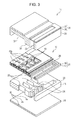
- Fig. 3 is an exploded perspective view illustrating the head unit 11.
- Fig. 4 is a top view illustrating a piezoelectric layer 28 in piezoelectric elements 19
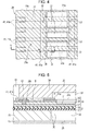
- Fig. 5 is a cross-sectional view illustrating the head unit 11 taken along a line V-V in Fig. 4 .
- each drawing following Fig. 3 partially illustrates a configuration corresponding to one of a total of two rows of nozzles (right side in Fig. 2 ) which are provided in the head unit 11.
- the head unit 11 in the embodiment is configured by laminating a flow channel forming substrate 15 (a kind of a pressure chamber forming member in the invention), a nozzle plate 16, an actuator unit 14, a sealing board 20 (a kind of sealing member in the invention), and the like.
- the flow channel forming substrate 15 is a plate material which includes a silicon single crystal substrate in which orientation of the surface is (110) in the embodiment.
- a plurality of pressure chambers 22 are formed to be arranged in a nozzle row direction by anisotropic etching.
- the pressure chambers 22 in the embodiment are empty portions which are long in a direction intersecting a direction in which the pressure chambers are disposed in parallel. Division is performed on the pressure chambers 22 in the embodiment by two (111) surfaces which are perpendicular to the (110) surface of the flow channel forming substrate 15 by the anisotropic etching.
- the two (111) surfaces intersects each other at a predetermined angle. Therefore, the opening shapes of the pressure chambers 22 when viewed from a direction which are perpendicular to the flow channel forming substrate 15 (a direction in which the head unit configuration members are laminated) are approximately polygonal shapes, more specifically, have approximately parallelogram shapes.
- Each of the pressure chambers 22 is provided to correspond to one of the nozzles 25 in the nozzle plate 16 one to one. That is, the pitch of forming each of the pressure chambers 22 corresponds to the pitch of forming the nozzles 25.
- communication portions 23 which pass through the flow channel forming substrate 15 are formed in a series along the direction in which the pressure chambers 22 are disposed in regions which are separated from the pressure chambers 22 on the sides of the pressure chambers in the pressure chamber's longitudinal direction (opposite sides to the sides which communicate with the nozzles).
- the communication portions 23 are empty portions which are common to the respective pressure chambers 22.
- the communication portions 23 communicate with the respective pressure chambers 22 through ink supply paths 24.
- each ink supply path 24 is formed with a width which is narrower than that of each pressure chamber 22, and corresponds to a portion that becomes passage resistance of ink which flows from the communication portion 23 into the pressure chamber 22.
- the nozzle plate 16 is bonded to the lower surface (surface which is opposite to a surface to which the actuator unit 14 is bonded) of the flow channel forming substrate 15 through an adhesive, a thermal welding film, or the like.
- the nozzle plate 16 is a plate in which the plurality of nozzles 25 are established in row shapes with a predetermined pitch.
- 360 nozzles 25 are arranged in a row with a pitch corresponding to 360 dpi, and thus a nozzle row (a kind of a nozzle group) is configured.
- Each of the nozzles 25 communicates with one of the pressure chambers 22 at an end portion on a side which is opposite to each of the ink supply paths 24.
- the nozzle plate 16 is configured from, for example, a glass ceramic, a silicon single crystal substrate, stainless steel, or the like.
- a total of two nozzle rows are provided in the head unit 11 in the embodiment, and liquid flow channels corresponding to the respective nozzle rows are provided to be symmetrical while interposing the sides of the nozzles 25.
- the actuator unit 14 in the embodiment is configured to include a vibration plate 21, piezoelectric elements 19, and metal layers 41.
- the vibration plate 21 includes an elastic film 17 which is formed on the upper surface of the flow channel forming substrate 15 and is formed of a silicon oxide (SiO 2 ), and an insulation film 18 which is formed on the elastic film 17 and is formed of zirconium oxide (ZrO 2 ).
- the portions of the vibration plate 21, which correspond to the pressure chambers 22, that is, portions which cover the upper openings of the pressure chambers 22 are displaced in a direction which is away from the nozzles 25 or which is close to the nozzles 25 in accordance with the bending deformation of the piezoelectric elements 19.
- the communication opening portion 26 which communicates with the communication portion 23 is provided in a portion corresponding to the communication portion 23 of the flow channel forming substrate 15 in the vibration plate 21. Meanwhile, it is possible to use a configuration which causes a part of the flow channel forming substrate 15 to function as the elastic film of the vibration plate 21 by processing the part to be thin.
- the piezoelectric elements 19 are formed on portions of the insulation film 18 of the vibration plate 21, which correspond to the pressure chambers 22.
- Each of the piezoelectric elements 19 in the embodiment is configured by sequentially laminating a lower electrode 27 (corresponding to a first electrode in the invention), a piezoelectric layer 28, and an upper electrode 29 (corresponding to a second electrode in the invention) from the side of the vibration plate 21.
- the lower electrode 27 in the embodiment is patterned in a long narrow strip form for each pressure chamber 22, and becomes an individual electrode for an active portion of each of the piezoelectric element 19.
- the upper electrode 29 is an electrode which is common to each of the piezoelectric elements 19 in the same row and is formed in a series along the direction in which each of the piezoelectric elements is disposed.
- the dimension of a direction of the upper electrode 29 (the longitudinal direction of the pressure chamber) which is perpendicular to the direction in which the piezoelectric elements are disposed is set to be slightly larger than the dimension of the opening sections of the pressure chambers 22 in the same direction. Further, in a direction in which the configuration members of each of the piezoelectric elements 19 are laminated, a portion in which the upper electrode 29, the piezoelectric layer 28, and the lower electrode 27 overlap with each other is the active portion in which piezoelectric deformation is generated when a voltage is supplied to both the electrodes. That is, the upper electrode 29 is the common electrode of the piezoelectric element 19, and the lower electrode 27 is the individual electrode of the piezoelectric element 19. Meanwhile, the upper electrode 29 and the lower electrode 27 can be configured to be reversed according to the circumstance of a driving circuit or a wiring.
- the piezoelectric layer 28 in the embodiment is formed on the vibration plate 21 so as to cover the entire surface of the lower electrode 27.
- the piezoelectric layer 28 it is possible to use a substance which includes lead (Pb), titanium (Ti), and a zirconium (Zr), for example, a ferroelectric piezoelectric material, such as lead zirconate titanate (PZT), or a substance acquired by adding metallic oxide, such as niobium oxide, nickel oxide, or magnesium, thereto.
- PZT lead zirconate titanate
- hollows 31 are formed in portions corresponding to regions interposed between adjacent pressure chambers 22 in the piezoelectric layer 28, that is, portions corresponding to walls 22a (refer to Fig.
- the hollows 31 are configured from depressions or through holes which are formed by partially removing the piezoelectric layer 28, and extend along the sides (opening edges) of the pressure chambers 22.
- the hollows 31 are portions which have a relatively thinner thickness than other portions of the piezoelectric layer 28 or portions which pass through the piezoelectric layer 28.
- the dimensions of the hollows 31 in the longitudinal direction are set to be shorter than the dimensions of the opening portions of the pressure chambers 22 in the longitudinal direction, and the hollows 31 are formed in regions along the sides of the openings of the pressure chambers 22 in regions interposed between the adjacent pressure chambers 22.
- the hollows 31 are formed in portions which are regions interposed between adjacent pressure chambers 22 and which are not interposed between the corners 30 (also called corner portions or corner angle portions) of the chambers 22, that is, in positions which are interposed between the sides of the opening portions of both pressure chambers 22.
- each of the opening portions of the pressure chambers 22 mean edges in a substantially straight form which connects the corners 30 of the opening of the pressure chamber 22 or edges (peripheral edge portions) which connect the corners 30 and are sufficiently gently bent compared to the corners 30.
- each of the hollows 31 in the width direction is set to be a little larger than the width of each of the walls 22a in the embodiment. That is, both edge portions of each of the hollows 31 in the width direction are partially overlapped with the opening section of each of the pressure chambers 22.
- regions along the corners 30 are relatively thicker than the piezoelectric layer 28 in the hollows 31.
- regions, which are interposed in such a way that the corners are positioned on at least one side between the adjacent pressure chambers 22, are relatively thicker than the thickness of the piezoelectric layer 28 in the hollows 31.
- the piezoelectric layer 28 which is thicker than the hollows 31 is provided in a beam shape in positions over the opening portions of the pressure chambers 22 in regions between the adjacent hollows 31.
- the width of the piezoelectric layer 28 of the portions in the direction in which the pressure chambers are disposed in parallel is slightly narrower than the widths of the opening portions of the pressure chambers 22 in the same direction.
- the width of the piezoelectric layer 28 which configures the active portions in beam-shaped portions is narrower than the widths of the pressure chambers 22, and thus it is further easy to move the piezoelectric layer 28 and it is possible to further effectively apply pressure variation with respect to ink in the pressure chambers 22.
- the active portions of the piezoelectric elements 19 are defined by portions in which the upper electrode 29, the piezoelectric layer 28, and the lower electrode 27 are overlapped with each other.
- the hollows 31 are provided as described above, the beam-shaped piezoelectric layer 28 in ranges which are interposed between the adjacent hollows 31, and the upper and lower electrodes 27 and 29 thereof substantially function as the active portions.
- the hollows 31 are not provided in the vicinity of the corners 30 of each of the pressure chambers 22 on which stress is easily concentrated, and the corners 30 are covered by piezoelectric layer 28.
- the invention is suitable for such a configuration. Meanwhile, a range of forming the hollows 31 may avoid at least sharp corners 30 and the hollows 31 may be overlapped with dull corners 30.
- the upper electrode 29 includes a main body portion 29a which defines the active portion, and a conductive portion 29b which is separated from the main body portion 29a.
- the conductive portion 29b is present on the piezoelectric layer 28 in a region which is separated from the opening edge of the pressure chamber 22 in the longitudinal direction of the pressure chamber and is positioned on the other nozzle row side. Further, the conductive portion 29b corresponds to the lower electrode 27 and is independently formed in a position which has a predetermined interval from the main body portion 29a. Further, as shown in Fig. 5 , a through hole 42, which reaches the lower electrode 27 from the upper surface of the conductive portion 29b while passing through the conductive portion 29b and the piezoelectric layer 28, is formed.
- a metal layer 41 which is formed of gold (Au) is formed on the upper electrode 29 through an adhesion layer (for example, NiCr) which is not shown in the drawing.
- the metal layer 41 is configured from weight portions 41a and lead electrode portions 41b (a kind of an element terminal portion).
- Each of the weight portions 41a is a kind of a laminated material of the invention, and is a strip-shaped member which extends along the direction in which the piezoelectric elements are arranged in rows over the plurality of piezoelectric elements 19.
- the weight portions 41a are respectively formed in both end portions of each of the upper opening portions of the pressure chambers 22 in the longitudinal direction on the main body portion 29a of the upper electrode 29.
- the weight portions 41a are formed in positions which overlap with at least one corner 30 of each the opening portions of the pressure chambers 22.
- the weight portions 41a are respectively provided in a position which overlaps with two corners 30 of one end (another nozzle row side) of each of the opening portions in the longitudinal direction and a position which overlaps with one corner 30 on the other end portion of each of the opening portions in the longitudinal direction.
- the total thickness of the portions in each of the piezoelectric elements 19 with the weight portions 41a is relatively thicker than the total thickness of the portions corresponding to each of the opening portions of the pressure chambers 22. Further, the weight portions 41a control the displacement of both ends of each of the active portions of the piezoelectric elements 19 in the longitudinal direction, thereby suppressing the irregular displacement of the piezoelectric elements 19 when the piezoelectric elements 19 are driven.
- each of the piezoelectric elements 19 includes the corners 30 in the end portions thereof in the longitudinal direction and at least any one of sides which configure the corners 30 is inclined in the direction in which the pressure chambers are disposed in parallel or the longitudinal direction of the pressure chambers, unintended directional deformation of both end portions of each of the piezoelectric elements 19 in the longitudinal direction due to the effect of the inclined side is suppressed.
- Each of the lead electrode portions 41b is patterned in correspondence to the lower electrode 27 which is the individual electrode, and is formed such that at least a part thereof overlaps with the upper portion of each of the conductive portions 29b.
- the lead electrode portion 41b is electrically conducted to the lower electrode 27 through the through hole 42. Further, a driving voltage (driving pulse) is selectively applied to each of the piezoelectric elements 19 through the lead electrode portion 41b.
- the weight portion 41a and the lead electrode portion 41b are formed in the same process, and the respective upper surfaces thereof (surfaces) are aligned on the same surface.
- at least one of the lead electrode portions 41b is electrically conducted to the upper electrode 29 which is the common electrode, and functions as a common electrode terminal.
- the upper electrode 29 is removed and a part of the piezoelectric layer 28 is exposed in a region between the main body portion 29a of the upper electrode 29 and the conductive portion 29b, or in a region between the weight portion 41a and the lead electrode portion 41b (in a configuration which does not include the weight portion 41a, between the main body portion 29a of the upper electrode 29 and the lead electrode portion 41b).
- the exposed portions of the piezoelectric layer 28 in which the upper electrode 29 and the metal layer 41 are not formed are called exposed portions 28a.
- the sealing board 20 which includes an empty reception portion 32 capable of receiving the piezoelectric elements 19, is bonded to the upper surface of the actuator unit 14, which is on the opposite side of the lower surface bonded to the flow channel forming substrate 15.
- the sealing board 20 is a hollow box-shaped member in which the empty reception portion 32 is open toward the lower surface side which is bonded to the actuator unit 14.
- the empty reception portion 32 is a hollow which is formed from the lower surface side of the sealing board 20 toward the upper surface side thereof in the middle of the height direction of the sealing board 20.
- the inside measurement of the empty reception portion 32 in the nozzle row direction (direction in which the pressure chambers are disposed in parallel) is set to a size capable of receiving all of the piezoelectric elements 19 in the same row.
- the dimension of the empty reception portion 32 in a direction which is perpendicular to the nozzle row is set to be slightly larger than the dimension of each of the pressure chambers 22 in the same direction (longitudinal direction) and smaller than the dimension of the piezoelectric layer 28 in the same direction.
- the sealing board 20 is provided with an empty liquid chamber portion 33 in a position which is separated from the empty reception portion 32 on the outer side of the longitudinal direction of each of the pressure chambers and in a region which corresponds to the communication opening portion 26 of the vibration plate 21 and the communication portion 23 of the flow channel forming substrate 15.
- the empty liquid chamber portion 33 is provided along the direction in which the pressure chambers are arrayed in parallel while passing through the sealing board 20 in the thickness direction, and communicates with the communication opening portion 26 and the communication portion 23, thereby forming a reservoir which is a common ink chamber of each of the pressure chambers 22.
- the empty reception portion 32 and the empty liquid chamber portion 33 are separated by a panel wall 34.
- the lower surface of the sealing board 20 which includes the lower end surface of the panel wall 34 is bonded to the upper surface of the actuator unit 14 through adhesive B as shown in Fig. 5 .
- the adhesive B is formed of, for example, epoxy adhesive, and is transferred to and coated on the lower surface of the sealing board 20 in advance.
- the lower end surface of the sealing board 20 is bonded to the weight portion 41a which is provided on the other sides of the pressure chambers 22 in the longitudinal direction (that is, the supply path 24 sides of the pressure chambers 22) through the adhesive.
- the exposed portions 28a of the piezoelectric layer 28 which are exposed between the main body portion 29a of the upper electrode 29 or the weight portion 41a and the lead electrode portions 41b are covered by the adhesive B.
- the sealing board 20 is bonded to positions which correspond to the corners 30 of each of the pressure chambers 22 and portions which have a total thickness that is relatively thick by providing the weight portions 41a.
- Fig. 5 shows an arrangement in which the bonded portion of the sealing board 20 directly covers only the acute corner 30 on the left hand side and not the obtuse corner 30, shown to the right of it in Fig. 5 , which is at the same end of the pressure chamber 22. However, it would also be possible to bond the sealing board 20 over both these corners.
- a silicon single crystal substrate which is the flow channel forming substrate 15 is thermally oxidized in a diffusion furnace at approximately 1100°C, and a silicon dioxide (SiO 2 ) film which configures the elastic film 17 is formed on the surface thereof.
- the insulation film 18 which is formed of zirconium oxide (ZrO 2 ) is formed on the elastic film 17. More specifically, first, a zirconium layer is formed on the elastic film 17 using, for example, a DC sputtering method, and the insulation film 18 which is formed of zirconium oxide is formed in such a way that the zirconium layer is thermally oxidized.
- the lower electrode 27 is formed by laminating, for example, platinum (Pt) and iridium (Ir) on the insulation film 18, and is patterned so as to have a width which is smaller than the width of the pressure chamber 22.
- the piezoelectric layer 28 which is formed of lead zirconate titanate (PZT) is laminated on the surface of the lower electrode 27.
- PZT lead zirconate titanate
- a so-called sol-gel method is used to form the piezoelectric layer 28 by gelling a so-called sol in which a metal organic material is dissolved and scattered in a solvent through coating and drying and by baking the sol at a high temperature.
- the method of forming the piezoelectric layer 28 is not particularly limited. For example, a MOD method, a sputtering method, or the like can be used.
- the upper electrode 29 which is formed of, for example, iridium is formed on the upper surface of the piezoelectric layer 28 using a sputtering method or the like.
- the piezoelectric layer 28 and the upper electrode 29 are patterned using dry etching, for example, reactive ion etching, ion milling, or the like. More specifically, the upper electrode 29 is patterned into the main body portion 29a and the conductive portion 29b. Further, the hollow 31 and the through hole 42 are formed in the upper electrode 29 and the piezoelectric layer 28. Subsequently, as shown in Fig. 7B , the metal layer 41 is formed on the upper electrode 29 through an adhesion layer which is not shown in the drawing using a sputtering method, a vacuum evaporation method, a CVD method or the like.
- the metal layer 41 is patterned into the weight portion 41a and the lead electrode portion 41b by etching or the like. Subsequently, the sealing board 20 is bonded to the actuator unit 14. As described above, when the sealing board 20 is bonded to the actuator unit 14, the lower end surface of the panel wall 34 is bonded to the weight portion 41a and the lead electrode portion 41b while straddling the exposed portions 28a of the piezoelectric layer 28. Therefore, the exposed portion 28a of the piezoelectric layer 28 is covered by the sealing board 20 and the adhesive B.
- the head unit 11 acquired in a state before the pressure chamber 22 is formed, is soaked by etching liquid, and the flow channel, such as the pressure chamber 22 or the ink supply path 24, is formed by etching on the flow channel forming substrate 15. If the flow channel, such as the pressure chamber 22, is formed, a process of bonding the nozzle plate 16 to the flow channel forming substrate 15 is performed (refer to Fig. 5 ).
- the invention is not limited thereto. In brief, it is possible to apply the invention to a configuration which includes a pressure chamber that has a polygonal opening shape having a plurality of corners.
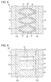
- Fig. 8 is a plan view illustrating a piezoelectric layer 28' which shows a configuration according to a second embodiment of the invention. Meanwhile, for convenience, unnecessary configurations will not be described.
- the opening shapes of the pressure chambers 22' (shown by dotted lines in Fig. 8 ) approximate to diamond shapes, and adjacent pressure chambers 22' are disposed with aligned corners 30'. Unlike the corners 30 in the first embodiment, the corners 30' are different from corners which are acquired in such a way that a straight line intersects a straight line, and instead are configured to include curved lines which have predetermined curvature.
- hollows 31' are formed along the respective sides in regions which are interposed between the sides of the pressure chambers 22'. More specifically, the hollows 31' are formed along the respective sides such that the hollows correspond to substantially straight sides of the opening portions of the respective pressure chambers 22'. That is, with regard to a single pressure chamber 22', a total of four hollows 31' are arranged to surround the opening portion of the pressure chamber 22'. The entire length of each hollow 31' is shorter than the length of a corresponding side. Therefore, similar to the first embodiment, a region acquired along the corners 30' is relatively thicker than the thickness of the piezoelectric layer 28' in the hollows 31'.
- a region which includes at least one side in which the corner 30' is located and which is interposed between the adjacent pressure chambers 22', is relatively thicker than the thickness of the piezoelectric layer 28' in the hollows 31.
- weight portions 41a' are respectively provided in positions which overlap with the corners 30' which are located in both end portions of the opening portion of the pressure chamber 22' in the longitudinal direction.
- the total thickness of the portions is relatively thicker than the total thickness of other portions, and thus it is possible to suppress the irregular displacement of the piezoelectric elements 19 when the piezoelectric elements 19 are driven.
- the hollow 31' it is possible to use a configuration in which a part of the hollows 31' overlaps with the opening portion of the pressure chamber 22' as shown by broken lines in Fig. 8 .
- Fig. 9 is a plan view illustrating a piezoelectric layer 28" which shows a configuration according to a third embodiment of the invention. Meanwhile, similar to the second embodiment, unnecessary configurations will not be described.
- the opening shape of a pressure chamber 22" (shown by dotted lines in Fig. 9 ) is an approximately parallelogram shape which is configured to mainly have a gentle curved line.
- portions which have the maximum curvature and a second maximum curvature compared to other portions are defined as corners 30", and the other portions which have relatively smooth curved lines are defined as sides.
- a hollow 31" is formed in a region which is interposed between the sides of the respective pressure chambers 22" along the sides.
- the width of the hollow 31" is set to be slightly larger than walls which perform division on (in other words, divide) the pressure chambers 22", and the portions of the hollow 31" overlap with the opening portions of the respective pressure chamber 22".
- the entire length of each hollow 31" is shorter than the length of the corresponding sides. Therefore, similar to the first embodiment and the second embodiment, a region acquired along the corners 30" is relatively thicker than the thickness of the piezoelectric layer 28" in the hollows 31".
- weight portions 41a" are respectively provided in positions which overlap with the corners 30" which are located in both end portions of the opening portion of the pressure chamber 22" in the longitudinal direction and have the maximum curvature.
- an ink jet type recording head which is mounted on an ink jet printer is exemplified.
- piezoelectric elements having such a configuration it is possible to apply the invention to a device which ejects liquid other than ink.
- a color material ejecting head which is used to manufacture color filters of a liquid crystal display or the like
- an electrode material ejecting head which is used to form electrodes of an organic Electro Luminescence (EL) display, a Field Emission Display (FED), or the like
- EL organic Electro Luminescence
- FED Field Emission Display
Landscapes
- Particle Formation And Scattering Control In Inkjet Printers (AREA)
Abstract
Description
- The present invention relates to a liquid ejecting head which ejects liquid by driving piezoelectric elements and a liquid ejecting apparatus including the same, and, more particularly, to a liquid ejecting head capable of preventing the damage of configuration members due to stress generated when piezoelectric elements are driven, and a liquid ejecting apparatus.
- A liquid ejecting apparatus is an apparatus which includes a liquid ejecting head and which ejects various types of liquid from the ejecting head. As the liquid ejecting apparatus, there are, for example, image recording apparatuses, such as an inkjet type printer or an ink jet type plotter. In recent years, such a liquid ejecting apparatus is applied to various types of manufacturing apparatuses by utilizing an advantage in that it is possible to accurately impact an extremely small amount of liquid in a predetermined position. For example, such a liquid ejecting apparatus is applied to a display manufacturing apparatus which is used to manufacture color filters of a liquid crystal display or the like, an electrode forming apparatus which is used to form electrodes of an organic Electro Luminescence (EL) display, a Field Emission Display (FED), or the like, and a chip manufacturing apparatus which is used to a manufacture biochip. Further, liquefied ink is ejected from a recording head for the image recording apparatus, and solutions of respective color materials, that are, R (Red), G (Green), and B (Blue) are ejected from a color material ejecting head for the display manufacturing apparatus. In addition, liquefied electrode material is ejected from an electrode material ejecting head for the electrode forming apparatus, and a bio organic substance solution is ejected from a bio organic substance ejecting head for the chip manufacturing apparatus.
- The liquid ejecting head is configured to introduce liquid into pressure chambers, generate change in pressure of the liquid in the pressure chambers, and eject the liquid from nozzles which communicate with the pressure chambers. The pressure chambers are formed in a silicon crystalline substrate (hereinafter, referred to as a pressure chamber forming substrate) by anisotropic etching with excellent dimensional accuracy. In addition, piezoelectric elements are preferably used as a pressure generation section which generates change in pressure of the liquid in the pressure chambers. There are various configurations of such a piezoelectric element. For example, a piezoelectric element is configured in such a way that a lower electrode on a side close to the pressure chamber, a piezoelectric layer which is formed of a piezoelectric material, such as lead zirconate titanate (PZT), and an upper electrode are respectively laminated and patterned using a film formation technology. Further, one of the upper and lower electrodes functions as an individual electrode which is provided for each pressure chamber, and a remaining one functions as a common electrode which is common to a plurality of pressure chambers. With regard to the piezoelectric film, a portion which is interposed between the upper and lower electrodes is an active portion which deforms due to the supply of a voltage to the electrodes, and a portion which is separated from one or both of the upper and lower electrodes is an inactive portion which does not deform due to the supply of the voltage to the electrodes.
- As the liquid ejecting head, a configuration is proposed in which a piezoelectric layer is formed in a series in a state in which openings of a plurality of pressure chambers are covered on a pressure chamber forming substrate (for example, refer to
JP-A-2003-311954 JP-A-2003-311954 - However, in the related-art configuration, stress is concentrated on corners of an opening portion of a pressure chamber which has a polygonal shape, more specifically, on sharp corners in accordance with the deformation of the active portion, and thus there is a problem in that damage, such as cracks, may occur in a pressure chamber forming substrate which is configured from a silicon substrate or a head configuration member, such as a piezoelectric layer.
- An advantage of some aspects of the invention is to provide a liquid ejecting head and a liquid ejecting apparatus which are capable of preventing configuration members from being damaged by reducing stress concentration when piezoelectric elements are driven.
- According to an aspect of the invention, there is provided a liquid ejecting head including: a pressure chamber forming member that is formed with pressure chambers which communicate with nozzles; and a piezoelectric element that includes a first electrode, a piezoelectric layer, and a second electrode which are laminated in a position corresponding to an opening portion of each of the pressure chambers in the pressure chamber forming member in a sequence from a side close to the opening portion. The opening portion of each of the pressure chambers has a polygonal shape which has a plurality of corners and sides that connect the corners to each other, the piezoelectric layer is integrally formed throughout the plurality of pressure chambers in the pressure chamber forming member, a predetermined region along the sides from among regions which are interposed between adjacent pressure chambers includes a hollow that penetrates the piezoelectric layer or a hollow that has a relatively thin thickness in the piezoelectric layer, and a predetermined region along the corners is relatively thicker than the thickness of the piezoelectric layer in the hollow.
- Meanwhile, the positional relationship between each of the pressure chambers (pressure chamber forming member) and the piezoelectric layer according to the aspect includes a configuration which is in a laminating relation in a state in which another member, such as the vibration plate, is interposed therebetween. In addition, "correspond" indicates that each of the members is in a positional relationship which overlaps with each other when viewed from a laminating direction.
- In addition, according to another aspect of the invention, there is provided a liquid ejecting head including: a pressure chamber forming member that is formed with pressure chambers which communicate with nozzles; and a piezoelectric element that includes a first electrode, a piezoelectric layer, and a second electrode which are laminated in a position corresponding to an opening portion of each of the pressure chambers in the pressure chamber forming member in a sequence from a side close to the opening portion. The opening portion of each of the pressure chambers has a polygonal shape which has a plurality of corners and sides that connect the corners to each other, the piezoelectric layer is integrally formed throughout the plurality of pressure chambers in the pressure chamber forming member, a region that is interposed between sides from among regions which are interposed between adjacent pressure chambers has a hollow that penetrates the piezoelectric layer or a hollow that has a relatively thin thickness in the piezoelectric layer, and a region, that is interposed in such a way that the corners are positioned on at least one side, is relatively thicker than the thickness of the piezoelectric layer in the hollow.
- In the liquid ejecting head according to the invention, in a region along the sides of the adjacent pressure chambers in the piezoelectric layer, a hollow is formed along the sides. The region along the corners on which the stress of the pressure chambers is easily concentrated, that is, the region which is interposed in such a way that the corner of at least one side of the opening portion is positioned is covered by the piezoelectric layer which is relatively thicker than the thickness of the piezoelectric layer in the hollow. Therefore, stress, generated when the active portion of the piezoelectric element is driven, hardly concentrated on the corners of the pressure chambers, and thus it is possible to suppress the damage of a configuration member, such as the pressure chamber forming member or the piezoelectric element. In particular, in a case of a sharp corner, although stress is easily concentrated on the corner, the invention is suitable for such a configuration.
- In the liquid ejecting head, in a position that is a region interposed between adjacent hollows and that corresponds to the opening portion of each of the pressure chambers, the piezoelectric layer which is thicker than thickness of the piezoelectric layer in the hollows may be provided, and a width of the piezoelectric layer in the position in a direction in which the pressure chambers may be disposed in parallel is narrower than a width of the opening portion of each of the pressure chambers in a same direction.
- In the liquid ejecting head, the piezoelectric layer which is provided in a position corresponding to the opening portion of each of the pressure chambers is further easily moved, and thus it is possible to further effectively apply pressure variation with respect to liquid in the pressure chambers.
- In addition, on the piezoelectric layer that is positioned on both sides of the opening portion of each of the pressure chambers in a direction intersecting a direction in which the pressure chambers are disposed in parallel and that covers at least one corner, a laminated material which causes a total thickness of the portion to be relatively thicker than other portions may be provided.
- In the liquid ejecting head, the laminated material, which causes the total thickness of the portion to be relatively thicker than other portions, is provided on the piezoelectric layer which is positioned on both sides of the opening portion of each of the pressure chambers in a direction intersecting a direction in which the pressure chambers are disposed in parallel and which covers at least one corner, with the result that the laminated material limits the displacement of both end portions of the piezoelectric element, and thus it is possible to suppress the irregular displacement of the piezoelectric element when the piezoelectric element is driven.
- In addition, in the liquid ejecting head, the laminated material may be a metal film, and may be formed in a series along a first direction in order to electrically conduct to the second electrode of the plurality of piezoelectric elements.
- In the liquid ejecting head, the laminated material is a metal film, and is electrically conducted to the second electrode of a plurality of piezoelectric elements which are formed in a series along the first direction, and thus it is possible to increase current capacity of the second electrode which is provided to be common to each of the piezoelectric elements.
- In addition, the liquid ejecting head may further include a sealing member that has an empty portion therein, which is capable of receiving an active portion in which the first electrode, the piezoelectric layer, and the second electrode are superimposed on each other. The sealing member may be bonded to the laminated material in a state in which the active portion is received in the empty portion.
- In the liquid ejecting head, the sealing member is bonded to the portion that has the total thickness which is relatively thick by providing the laminated material, with the result that it is possible to further suppress the deformation other than the active portion of the piezoelectric element, and thus it is possible to further securely suppress the generation of damage, such as cracks, of the configuration member, such as the pressure chamber forming member or the piezoelectric element. In addition, a hollow is not provided on a portion to which the sealing member is bonded and the piezoelectric layer of the portion has a flat surface, and thus it is possible to bond the sealing member in a stable state.
- Further, according to another aspect of the invention, there is provided a liquid ejecting apparatus that includes the liquid ejecting head which has any of the above configurations.
- Embodiments of the invention will now be described by way of example only with reference to the accompanying drawings, wherein like numbers reference like elements.
-
Fig. 1 is a perspective view illustrating a configuration of a printer. -
Fig. 2 is a cross-sectional view illustrating a head unit. -
Fig. 3 is an exploded perspective view illustrating the head unit. -
Fig. 4 is a plan view illustrating a piezoelectric layer. -
Fig. 5 is a cross-sectional view illustrating the head unit taken along a line V-V inFig. 4 . -
Figs. 6A to 6E are cross-sectional views illustrating main portions of a process of manufacturing the head unit. -
Figs. 7A to 7C are cross-sectional views illustrating the main portions of the process of manufacturing the head unit. -
Fig. 8 is a plan view illustrating a piezoelectric layer which shows a configuration according to a second embodiment. -
Fig. 9 is a plan view illustrating a piezoelectric layer which shows a configuration according to a third embodiment. - Hereinafter, embodiments of the invention will be described with reference to the accompanying drawings. Meanwhile, in embodiments which will be described below, various limitations are applied as preferable appropriate examples of the invention. However, the scope of the invention is not limited to the embodiments if the invention is not particularly stated as being limited in the description below. In addition, in the description below, as a liquid ejecting apparatus according to the invention, an ink jet type printer (hereinafter, a printer), on which an ink jet type recording head (hereinafter, a recording head) that is a type of a liquid ejecting head is mounted, is exemplified.
- The configuration of a printer 1 will be described with reference to
Fig. 1 . The printer 1 is an apparatus which records an image or the like by ejecting liquefied ink onto the surface of a recording medium 2 (a kind of an impact target) such as recording paper. The printer 1 includes arecording head 3, a carriage 4 to which therecording head 3 is attached, acarriage moving mechanism 5 which moves the carriage 4 in a main scan direction, and a transport mechanism 6 which transports therecording medium 2 in a sub scan direction. Here, the ink is a kind of liquid in the invention and is stored in theink cartridge 7 as a liquid supply source. Theink cartridge 7 is detachably mounted on therecording head 3. Meanwhile, it is possible to use a configuration in which theink cartridge 7 is arranged on a main body side of the printer 1, and the ink is supplied to therecording head 3 from theink cartridge 7 through an ink supply tube. - The
carriage moving mechanism 5 includes atiming belt 8. Further, thetiming belt 8 is driven by apulse motor 9 such as a DC motor. Therefore, when thepulse motor 9 operates, the carriage 4 is guided through aguide rod 10 which is installed in the printer 1 and reciprocates in the main scan direction (in the width direction of the recording medium 2). -
Fig. 2 is a cross-sectional view illustrating an inside configuration of ahead unit 11 which is included in therecording head 3 in the embodiment, andFig. 3 is an exploded perspective view illustrating thehead unit 11. In addition,Fig. 4 is a top view illustrating apiezoelectric layer 28 inpiezoelectric elements 19, andFig. 5 is a cross-sectional view illustrating thehead unit 11 taken along a line V-V inFig. 4 . Meanwhile, each drawing followingFig. 3 partially illustrates a configuration corresponding to one of a total of two rows of nozzles (right side inFig. 2 ) which are provided in thehead unit 11. - The
head unit 11 in the embodiment is configured by laminating a flow channel forming substrate 15 (a kind of a pressure chamber forming member in the invention), anozzle plate 16, anactuator unit 14, a sealing board 20 (a kind of sealing member in the invention), and the like. - The flow
channel forming substrate 15 is a plate material which includes a silicon single crystal substrate in which orientation of the surface is (110) in the embodiment. In the flowchannel forming substrate 15, a plurality ofpressure chambers 22 are formed to be arranged in a nozzle row direction by anisotropic etching. Thepressure chambers 22 in the embodiment are empty portions which are long in a direction intersecting a direction in which the pressure chambers are disposed in parallel. Division is performed on thepressure chambers 22 in the embodiment by two (111) surfaces which are perpendicular to the (110) surface of the flowchannel forming substrate 15 by the anisotropic etching. The two (111) surfaces intersects each other at a predetermined angle. Therefore, the opening shapes of thepressure chambers 22 when viewed from a direction which are perpendicular to the flow channel forming substrate 15 (a direction in which the head unit configuration members are laminated) are approximately polygonal shapes, more specifically, have approximately parallelogram shapes. - Each of the
pressure chambers 22 is provided to correspond to one of thenozzles 25 in thenozzle plate 16 one to one. That is, the pitch of forming each of thepressure chambers 22 corresponds to the pitch of forming thenozzles 25. In addition, as shown inFig. 2 , in the flowchannel forming substrate 15,communication portions 23 which pass through the flowchannel forming substrate 15 are formed in a series along the direction in which thepressure chambers 22 are disposed in regions which are separated from thepressure chambers 22 on the sides of the pressure chambers in the pressure chamber's longitudinal direction (opposite sides to the sides which communicate with the nozzles). Thecommunication portions 23 are empty portions which are common to therespective pressure chambers 22. Thecommunication portions 23 communicate with therespective pressure chambers 22 throughink supply paths 24. Meanwhile, thecommunication portions 23 communicate with thecommunication opening portions 26 of thevibration plate 21 which will be described later and the emptyliquid chamber portions 33 of the sealingboard 20, and configure reservoirs (common liquid chambers) which are ink chambers common to therespective pressure chambers 22. Eachink supply path 24 is formed with a width which is narrower than that of eachpressure chamber 22, and corresponds to a portion that becomes passage resistance of ink which flows from thecommunication portion 23 into thepressure chamber 22. - The
nozzle plate 16 is bonded to the lower surface (surface which is opposite to a surface to which theactuator unit 14 is bonded) of the flowchannel forming substrate 15 through an adhesive, a thermal welding film, or the like. Thenozzle plate 16 is a plate in which the plurality ofnozzles 25 are established in row shapes with a predetermined pitch. In the embodiment, 360nozzles 25 are arranged in a row with a pitch corresponding to 360 dpi, and thus a nozzle row (a kind of a nozzle group) is configured. Each of thenozzles 25 communicates with one of thepressure chambers 22 at an end portion on a side which is opposite to each of theink supply paths 24. Meanwhile, thenozzle plate 16 is configured from, for example, a glass ceramic, a silicon single crystal substrate, stainless steel, or the like. A total of two nozzle rows are provided in thehead unit 11 in the embodiment, and liquid flow channels corresponding to the respective nozzle rows are provided to be symmetrical while interposing the sides of thenozzles 25. - The
actuator unit 14 in the embodiment is configured to include avibration plate 21,piezoelectric elements 19, and metal layers 41. Thevibration plate 21 includes anelastic film 17 which is formed on the upper surface of the flowchannel forming substrate 15 and is formed of a silicon oxide (SiO2), and aninsulation film 18 which is formed on theelastic film 17 and is formed of zirconium oxide (ZrO2). The portions of thevibration plate 21, which correspond to thepressure chambers 22, that is, portions which cover the upper openings of thepressure chambers 22 are displaced in a direction which is away from thenozzles 25 or which is close to thenozzles 25 in accordance with the bending deformation of thepiezoelectric elements 19. Thecommunication opening portion 26 which communicates with thecommunication portion 23 is provided in a portion corresponding to thecommunication portion 23 of the flowchannel forming substrate 15 in thevibration plate 21. Meanwhile, it is possible to use a configuration which causes a part of the flowchannel forming substrate 15 to function as the elastic film of thevibration plate 21 by processing the part to be thin. - The
piezoelectric elements 19 are formed on portions of theinsulation film 18 of thevibration plate 21, which correspond to thepressure chambers 22. Each of thepiezoelectric elements 19 in the embodiment is configured by sequentially laminating a lower electrode 27 (corresponding to a first electrode in the invention), apiezoelectric layer 28, and an upper electrode 29 (corresponding to a second electrode in the invention) from the side of thevibration plate 21. Thelower electrode 27 in the embodiment is patterned in a long narrow strip form for eachpressure chamber 22, and becomes an individual electrode for an active portion of each of thepiezoelectric element 19. In addition, theupper electrode 29 is an electrode which is common to each of thepiezoelectric elements 19 in the same row and is formed in a series along the direction in which each of the piezoelectric elements is disposed. The dimension of a direction of the upper electrode 29 (the longitudinal direction of the pressure chamber) which is perpendicular to the direction in which the piezoelectric elements are disposed is set to be slightly larger than the dimension of the opening sections of thepressure chambers 22 in the same direction. Further, in a direction in which the configuration members of each of thepiezoelectric elements 19 are laminated, a portion in which theupper electrode 29, thepiezoelectric layer 28, and thelower electrode 27 overlap with each other is the active portion in which piezoelectric deformation is generated when a voltage is supplied to both the electrodes. That is, theupper electrode 29 is the common electrode of thepiezoelectric element 19, and thelower electrode 27 is the individual electrode of thepiezoelectric element 19. Meanwhile, theupper electrode 29 and thelower electrode 27 can be configured to be reversed according to the circumstance of a driving circuit or a wiring. - The
piezoelectric layer 28 in the embodiment is formed on thevibration plate 21 so as to cover the entire surface of thelower electrode 27. As thepiezoelectric layer 28, it is possible to use a substance which includes lead (Pb), titanium (Ti), and a zirconium (Zr), for example, a ferroelectric piezoelectric material, such as lead zirconate titanate (PZT), or a substance acquired by adding metallic oxide, such as niobium oxide, nickel oxide, or magnesium, thereto. As shown inFig. 4 , hollows 31 are formed in portions corresponding to regions interposed betweenadjacent pressure chambers 22 in thepiezoelectric layer 28, that is, portions corresponding towalls 22a (refer toFig. 4 ) which perform division between the neighboringpressure chambers 22. Thehollows 31 are configured from depressions or through holes which are formed by partially removing thepiezoelectric layer 28, and extend along the sides (opening edges) of thepressure chambers 22. In conclusion, thehollows 31 are portions which have a relatively thinner thickness than other portions of thepiezoelectric layer 28 or portions which pass through thepiezoelectric layer 28. - Further, the dimensions of the
hollows 31 in the longitudinal direction are set to be shorter than the dimensions of the opening portions of thepressure chambers 22 in the longitudinal direction, and thehollows 31 are formed in regions along the sides of the openings of thepressure chambers 22 in regions interposed between theadjacent pressure chambers 22. In other words, thehollows 31 are formed in portions which are regions interposed betweenadjacent pressure chambers 22 and which are not interposed between the corners 30 (also called corner portions or corner angle portions) of thechambers 22, that is, in positions which are interposed between the sides of the opening portions of bothpressure chambers 22. Meanwhile, the "sides" of each of the opening portions of thepressure chambers 22 mean edges in a substantially straight form which connects thecorners 30 of the opening of thepressure chamber 22 or edges (peripheral edge portions) which connect thecorners 30 and are sufficiently gently bent compared to thecorners 30. - Therefore, when viewed in the direction in which the configuration members of the
head unit 11 are laminated, none of thecorners 30 are overlapped in each of thehollows 31 and all of thecorners 30 of the opening portion of each of thepressure chambers 22 are covered by thepiezoelectric layer 28. In addition, the dimension of each of thehollows 31 in the width direction (direction in which the pressure chambers are disposed in parallel) is set to be a little larger than the width of each of thewalls 22a in the embodiment. That is, both edge portions of each of thehollows 31 in the width direction are partially overlapped with the opening section of each of thepressure chambers 22. On the other hand, regions along thecorners 30 are relatively thicker than thepiezoelectric layer 28 in thehollows 31. That is, regions, which are interposed in such a way that the corners are positioned on at least one side between theadjacent pressure chambers 22, are relatively thicker than the thickness of thepiezoelectric layer 28 in thehollows 31. Further, thepiezoelectric layer 28 which is thicker than thehollows 31 is provided in a beam shape in positions over the opening portions of thepressure chambers 22 in regions between theadjacent hollows 31. The width of thepiezoelectric layer 28 of the portions in the direction in which the pressure chambers are disposed in parallel is slightly narrower than the widths of the opening portions of thepressure chambers 22 in the same direction. When thehollows 31 are provided on the both sides of the beam-shapedpiezoelectric layer 28, it is possible to smoothly displace thepiezoelectric layer 28 and it is possible to suppress unnecessary displacement of portions other than the beam-shapedpiezoelectric layer 28 which is a driving target. In the embodiment, the width of thepiezoelectric layer 28 which configures the active portions in beam-shaped portions is narrower than the widths of thepressure chambers 22, and thus it is further easy to move thepiezoelectric layer 28 and it is possible to further effectively apply pressure variation with respect to ink in thepressure chambers 22. - Here, the active portions of the
piezoelectric elements 19 are defined by portions in which theupper electrode 29, thepiezoelectric layer 28, and thelower electrode 27 are overlapped with each other. However, in a configuration in which thehollows 31 are provided as described above, the beam-shapedpiezoelectric layer 28 in ranges which are interposed between theadjacent hollows 31, and the upper andlower electrodes hollows 31 are not provided in the vicinity of thecorners 30 of each of thepressure chambers 22 on which stress is easily concentrated, and thecorners 30 are covered bypiezoelectric layer 28. Therefore, it is difficult for stress, generated when the active portions of thepiezoelectric elements 19 are driven, to concentrate on thecorners 30 of each of thepressure chambers 22, and thus it is possible to suppress the damage of the flowchannel forming substrate 15 which is formed of a silicon single crystal substrate, thevibration plate 21, or thepiezoelectric elements 19. In particular, similar to thepressure chambers 22 in the embodiment, when thecorners 30 are included in the end portions of each of the opening portions in the longitudinal direction and thecorners 30 aresharp corners 30, stress is easily concentrated on thecorners 30. However, the invention is suitable for such a configuration. Meanwhile, a range of forming thehollows 31 may avoid at leastsharp corners 30 and thehollows 31 may be overlapped withdull corners 30. - The
upper electrode 29 includes amain body portion 29a which defines the active portion, and aconductive portion 29b which is separated from themain body portion 29a. Theconductive portion 29b is present on thepiezoelectric layer 28 in a region which is separated from the opening edge of thepressure chamber 22 in the longitudinal direction of the pressure chamber and is positioned on the other nozzle row side. Further, theconductive portion 29b corresponds to thelower electrode 27 and is independently formed in a position which has a predetermined interval from themain body portion 29a. Further, as shown inFig. 5 , a throughhole 42, which reaches thelower electrode 27 from the upper surface of theconductive portion 29b while passing through theconductive portion 29b and thepiezoelectric layer 28, is formed. - A metal layer 41 which is formed of gold (Au) is formed on the
upper electrode 29 through an adhesion layer (for example, NiCr) which is not shown in the drawing. The metal layer 41 is configured fromweight portions 41a andlead electrode portions 41b (a kind of an element terminal portion). Each of theweight portions 41a is a kind of a laminated material of the invention, and is a strip-shaped member which extends along the direction in which the piezoelectric elements are arranged in rows over the plurality ofpiezoelectric elements 19. Theweight portions 41a are respectively formed in both end portions of each of the upper opening portions of thepressure chambers 22 in the longitudinal direction on themain body portion 29a of theupper electrode 29. More specifically, in a planar view, theweight portions 41a are formed in positions which overlap with at least onecorner 30 of each the opening portions of thepressure chambers 22. In the embodiment, theweight portions 41a are respectively provided in a position which overlaps with twocorners 30 of one end (another nozzle row side) of each of the opening portions in the longitudinal direction and a position which overlaps with onecorner 30 on the other end portion of each of the opening portions in the longitudinal direction. The total thickness of the portions in each of thepiezoelectric elements 19 with theweight portions 41a (entire thickness including thevibration plate 21, thelower electrode 27, thepiezoelectric layer 28, theupper electrode 29, and theweight portion 41a, which configure each of the piezoelectric elements 19) is relatively thicker than the total thickness of the portions corresponding to each of the opening portions of thepressure chambers 22. Further, theweight portions 41a control the displacement of both ends of each of the active portions of thepiezoelectric elements 19 in the longitudinal direction, thereby suppressing the irregular displacement of thepiezoelectric elements 19 when thepiezoelectric elements 19 are driven. In particular, similar to thepressure chambers 22 of the embodiment, when each of thepiezoelectric elements 19 includes thecorners 30 in the end portions thereof in the longitudinal direction and at least any one of sides which configure thecorners 30 is inclined in the direction in which the pressure chambers are disposed in parallel or the longitudinal direction of the pressure chambers, unintended directional deformation of both end portions of each of thepiezoelectric elements 19 in the longitudinal direction due to the effect of the inclined side is suppressed. - Each of the
lead electrode portions 41b is patterned in correspondence to thelower electrode 27 which is the individual electrode, and is formed such that at least a part thereof overlaps with the upper portion of each of theconductive portions 29b. Thelead electrode portion 41b is electrically conducted to thelower electrode 27 through the throughhole 42. Further, a driving voltage (driving pulse) is selectively applied to each of thepiezoelectric elements 19 through thelead electrode portion 41b. Theweight portion 41a and thelead electrode portion 41b are formed in the same process, and the respective upper surfaces thereof (surfaces) are aligned on the same surface. In addition, at least one of thelead electrode portions 41b is electrically conducted to theupper electrode 29 which is the common electrode, and functions as a common electrode terminal. - In the
head unit 11 having this configuration, theupper electrode 29 is removed and a part of thepiezoelectric layer 28 is exposed in a region between themain body portion 29a of theupper electrode 29 and theconductive portion 29b, or in a region between theweight portion 41a and thelead electrode portion 41b (in a configuration which does not include theweight portion 41a, between themain body portion 29a of theupper electrode 29 and thelead electrode portion 41b). Hereinafter, the exposed portions of thepiezoelectric layer 28 in which theupper electrode 29 and the metal layer 41 are not formed are called exposedportions 28a. - The sealing
board 20, which includes anempty reception portion 32 capable of receiving thepiezoelectric elements 19, is bonded to the upper surface of theactuator unit 14, which is on the opposite side of the lower surface bonded to the flowchannel forming substrate 15. The sealingboard 20 is a hollow box-shaped member in which theempty reception portion 32 is open toward the lower surface side which is bonded to theactuator unit 14. Theempty reception portion 32 is a hollow which is formed from the lower surface side of the sealingboard 20 toward the upper surface side thereof in the middle of the height direction of the sealingboard 20. The inside measurement of theempty reception portion 32 in the nozzle row direction (direction in which the pressure chambers are disposed in parallel) is set to a size capable of receiving all of thepiezoelectric elements 19 in the same row. In addition, the dimension of theempty reception portion 32 in a direction which is perpendicular to the nozzle row is set to be slightly larger than the dimension of each of thepressure chambers 22 in the same direction (longitudinal direction) and smaller than the dimension of thepiezoelectric layer 28 in the same direction. In addition, as shown inFigs. 2 and3 , the sealingboard 20 is provided with an emptyliquid chamber portion 33 in a position which is separated from theempty reception portion 32 on the outer side of the longitudinal direction of each of the pressure chambers and in a region which corresponds to thecommunication opening portion 26 of thevibration plate 21 and thecommunication portion 23 of the flowchannel forming substrate 15. The emptyliquid chamber portion 33 is provided along the direction in which the pressure chambers are arrayed in parallel while passing through the sealingboard 20 in the thickness direction, and communicates with thecommunication opening portion 26 and thecommunication portion 23, thereby forming a reservoir which is a common ink chamber of each of thepressure chambers 22. - The
empty reception portion 32 and the emptyliquid chamber portion 33 are separated by apanel wall 34. The lower surface of the sealingboard 20 which includes the lower end surface of thepanel wall 34 is bonded to the upper surface of theactuator unit 14 through adhesive B as shown inFig. 5 . The adhesive B is formed of, for example, epoxy adhesive, and is transferred to and coated on the lower surface of the sealingboard 20 in advance. When the sealingboard 20 is bonded to theactuator unit 14, the lower end surface of thepanel wall 34 is bonded to theweight portions 41a and thelead electrode portions 41b while straddling the exposedportions 28a as shown inFig. 5 . In the same manner, the lower end surface of the sealingboard 20 is bonded to theweight portion 41a which is provided on the other sides of thepressure chambers 22 in the longitudinal direction (that is, thesupply path 24 sides of the pressure chambers 22) through the adhesive. As described above, the exposedportions 28a of thepiezoelectric layer 28 which are exposed between themain body portion 29a of theupper electrode 29 or theweight portion 41a and thelead electrode portions 41b are covered by the adhesive B. As described above, the sealingboard 20 is bonded to positions which correspond to thecorners 30 of each of thepressure chambers 22 and portions which have a total thickness that is relatively thick by providing theweight portions 41a. Therefore, it is possible to suppress unnecessary displacement of thepiezoelectric elements 19 other than the active portions far more, and thus damage, such as cracks, of thepiezoelectric elements 19 is further securely suppressed from being generated. In addition, thehollows 31 are not provided in portions to which the sealingboard 20 is bonded and thepiezoelectric layer 28 in those portions has a flat surface, and thus it is possible to bond the sealingboard 20 in a stable state.Fig. 5 shows an arrangement in which the bonded portion of the sealingboard 20 directly covers only theacute corner 30 on the left hand side and not theobtuse corner 30, shown to the right of it inFig. 5 , which is at the same end of thepressure chamber 22. However, it would also be possible to bond the sealingboard 20 over both these corners. - Here, a method of manufacturing the
head unit 11 will be described. - First, as shown in
Fig. 6A , a silicon single crystal substrate which is the flowchannel forming substrate 15 is thermally oxidized in a diffusion furnace at approximately 1100°C, and a silicon dioxide (SiO2) film which configures theelastic film 17 is formed on the surface thereof. Subsequently, as shown inFig. 6B , theinsulation film 18 which is formed of zirconium oxide (ZrO2) is formed on theelastic film 17. More specifically, first, a zirconium layer is formed on theelastic film 17 using, for example, a DC sputtering method, and theinsulation film 18 which is formed of zirconium oxide is formed in such a way that the zirconium layer is thermally oxidized. Subsequently, as shown inFig. 6C , thelower electrode 27 is formed by laminating, for example, platinum (Pt) and iridium (Ir) on theinsulation film 18, and is patterned so as to have a width which is smaller than the width of thepressure chamber 22. - Subsequently, as shown in
Fig. 6D , thepiezoelectric layer 28 which is formed of lead zirconate titanate (PZT) is laminated on the surface of thelower electrode 27. In the embodiment, as a method of forming thepiezoelectric layer 28, a so-called sol-gel method is used to form thepiezoelectric layer 28 by gelling a so-called sol in which a metal organic material is dissolved and scattered in a solvent through coating and drying and by baking the sol at a high temperature. Meanwhile, the method of forming thepiezoelectric layer 28 is not particularly limited. For example, a MOD method, a sputtering method, or the like can be used. Subsequently, as shown inFig. 6E , theupper electrode 29 which is formed of, for example, iridium is formed on the upper surface of thepiezoelectric layer 28 using a sputtering method or the like. - Subsequently, as shown in
Fig. 7A , thepiezoelectric layer 28 and theupper electrode 29 are patterned using dry etching, for example, reactive ion etching, ion milling, or the like. More specifically, theupper electrode 29 is patterned into themain body portion 29a and theconductive portion 29b. Further, the hollow 31 and the throughhole 42 are formed in theupper electrode 29 and thepiezoelectric layer 28. Subsequently, as shown inFig. 7B , the metal layer 41 is formed on theupper electrode 29 through an adhesion layer which is not shown in the drawing using a sputtering method, a vacuum evaporation method, a CVD method or the like. The metal layer 41 is patterned into theweight portion 41a and thelead electrode portion 41b by etching or the like. Subsequently, the sealingboard 20 is bonded to theactuator unit 14. As described above, when the sealingboard 20 is bonded to theactuator unit 14, the lower end surface of thepanel wall 34 is bonded to theweight portion 41a and thelead electrode portion 41b while straddling the exposedportions 28a of thepiezoelectric layer 28. Therefore, the exposedportion 28a of thepiezoelectric layer 28 is covered by the sealingboard 20 and the adhesive B. Thereafter, in a state in which theactuator unit 14 and the sealingboard 20 are covered by a protective sheet which is not shown in the drawing, thehead unit 11, acquired in a state before thepressure chamber 22 is formed, is soaked by etching liquid, and the flow channel, such as thepressure chamber 22 or theink supply path 24, is formed by etching on the flowchannel forming substrate 15. If the flow channel, such as thepressure chamber 22, is formed, a process of bonding thenozzle plate 16 to the flowchannel forming substrate 15 is performed (refer toFig. 5 ). - Here, in the first embodiment, a configuration in which the opening shape of the
pressure chamber 22 is approximately a parallelogram is exemplified. However, the invention is not limited thereto. In brief, it is possible to apply the invention to a configuration which includes a pressure chamber that has a polygonal opening shape having a plurality of corners. -
Fig. 8 is a plan view illustrating a piezoelectric layer 28' which shows a configuration according to a second embodiment of the invention. Meanwhile, for convenience, unnecessary configurations will not be described. In the embodiment, the opening shapes of the pressure chambers 22' (shown by dotted lines inFig. 8 ) approximate to diamond shapes, and adjacent pressure chambers 22' are disposed with alignedcorners 30'. Unlike thecorners 30 in the first embodiment, thecorners 30' are different from corners which are acquired in such a way that a straight line intersects a straight line, and instead are configured to include curved lines which have predetermined curvature. Further, in the portion of the piezoelectric layer 28' which corresponds to regions between the adjacent pressure chambers 22', hollows 31' are formed along the respective sides in regions which are interposed between the sides of the pressure chambers 22'. More specifically, the hollows 31' are formed along the respective sides such that the hollows correspond to substantially straight sides of the opening portions of the respective pressure chambers 22'. That is, with regard to a single pressure chamber 22', a total of four hollows 31' are arranged to surround the opening portion of the pressure chamber 22'. The entire length of each hollow 31' is shorter than the length of a corresponding side. Therefore, similar to the first embodiment, a region acquired along thecorners 30' is relatively thicker than the thickness of the piezoelectric layer 28' in the hollows 31'. That is, a region, which includes at least one side in which thecorner 30' is located and which is interposed between the adjacent pressure chambers 22', is relatively thicker than the thickness of the piezoelectric layer 28' in thehollows 31. In the configuration of the embodiment, it is possible to smoothly displace the piezoelectric layer 28', and it is possible to suppress displacement of unnecessary portions of the piezoelectric layer 28' to be driven. In addition,weight portions 41a' are respectively provided in positions which overlap with thecorners 30' which are located in both end portions of the opening portion of the pressure chamber 22' in the longitudinal direction. When theweight portions 41a' are provided, the total thickness of the portions is relatively thicker than the total thickness of other portions, and thus it is possible to suppress the irregular displacement of thepiezoelectric elements 19 when thepiezoelectric elements 19 are driven. Meanwhile, with regard to the hollow 31', it is possible to use a configuration in which a part of the hollows 31' overlaps with the opening portion of the pressure chamber 22' as shown by broken lines inFig. 8 . -
Fig. 9 is a plan view illustrating apiezoelectric layer 28" which shows a configuration according to a third embodiment of the invention. Meanwhile, similar to the second embodiment, unnecessary configurations will not be described. In the embodiment, the opening shape of apressure chamber 22" (shown by dotted lines inFig. 9 ) is an approximately parallelogram shape which is configured to mainly have a gentle curved line. In the opening shape which is configured to have such a curved line, portions which have the maximum curvature and a second maximum curvature compared to other portions are defined ascorners 30", and the other portions which have relatively smooth curved lines are defined as sides. Further, in a region of thepiezoelectric layer 28" which corresponds to a region betweenadjacent pressure chambers 22", a hollow 31" is formed in a region which is interposed between the sides of therespective pressure chambers 22" along the sides. In the embodiment, the width of the hollow 31" is set to be slightly larger than walls which perform division on (in other words, divide) thepressure chambers 22", and the portions of the hollow 31" overlap with the opening portions of therespective pressure chamber 22". In addition, the entire length of each hollow 31" is shorter than the length of the corresponding sides. Therefore, similar to the first embodiment and the second embodiment, a region acquired along thecorners 30" is relatively thicker than the thickness of thepiezoelectric layer 28" in thehollows 31". That is, a region, which includes at least one side in which thecorner 30" is located and which is interposed between theadjacent pressure chambers 22", is relatively thicker than the thickness of thepiezoelectric layer 28" in thehollows 31". In the configuration of the embodiment, it is possible to smoothly displace thepiezoelectric layer 28", and it is possible to suppress displacement of unnecessary portions of thepiezoelectric layer 28" to be driven. In addition,weight portions 41a" are respectively provided in positions which overlap with thecorners 30" which are located in both end portions of the opening portion of thepressure chamber 22" in the longitudinal direction and have the maximum curvature. When theweight portions 41a" are provided, the total thickness of the portions is relatively thicker than the total thickness of other portions, and thus it is possible to suppress the irregular displacement of thepiezoelectric elements 19 when thepiezoelectric elements 19 are driven. - Meanwhile, the invention is not limited to the above-described embodiments. In addition, in the above-described embodiment, an ink jet type recording head which is mounted on an ink jet printer is exemplified. However, if piezoelectric elements having such a configuration are used, it is possible to apply the invention to a device which ejects liquid other than ink. For example, it is possible to apply the invention to a color material ejecting head which is used to manufacture color filters of a liquid crystal display or the like, an electrode material ejecting head which is used to form electrodes of an organic Electro Luminescence (EL) display, a Field Emission Display (FED), or the like, a bio organic substance ejecting head which is used to manufacture a biochip, and the like.
- Embodiments of the present invention will now be described by way of further example only and with reference to the accompanying drawings, in which:
Claims (7)
- A liquid ejecting head (3) comprising:a pressure chamber forming member (15) that is formed with pressure chambers (22) which communicate with nozzles (25); anda piezoelectric element (19) that includes a first electrode (27), a piezoelectric layer (28), and a second electrode (29) which are laminated in a position corresponding to an opening portion of each of the pressure chambers in the pressure chamber forming member in a sequence from a side close to the opening portion,wherein the opening portion of each of the pressure chambers has a polygonal shape which includes a plurality of corners (30) and sides that connect the corners to each other, andwherein the piezoelectric layer (28) is integrally formed throughout the plurality of pressure chambers in the pressure chamber forming member,wherein a predetermined region along the sides from among regions which are interposed between adjacent pressure chambers (22) includes a hollow (31) that penetrates the piezoelectric layer or a hollow (31) in which the piezoelectric layer has a relatively thin thickness, andwherein a predetermined region along the corners is relatively thicker than the thickness of the piezoelectric layer in the hollow.
- A liquid ejecting head (3) comprising:a pressure chamber forming member (15) that is formed with pressure chambers (22) which communicate with nozzles (25); anda piezoelectric element (19) that includes a first electrode (27), a piezoelectric layer (28), and a second electrode (29) which are laminated in a position corresponding to an opening portion of each of the pressure chambers in the pressure chamber forming member in a sequence from a side close to the opening portion,wherein the opening portion of each of the pressure chambers has a polygonal shape which includes a plurality of corners (30) and sides that connect the corners to each other,wherein the piezoelectric layer (28) is integrally formed throughout the plurality of pressure chambers in the pressure chamber forming member,wherein a region that is interposed between sides from among regions which are interposed between adjacent pressure chambers (22) includes a hollow (31) that penetrates the piezoelectric layer or a hollow in which the piezoelectric layer has a relatively thin thickness , andwherein a region, that is interposed in such a way that the corners are positioned on at least one side, is relatively thicker than the thickness of the piezoelectric layer in the hollow.
- The liquid ejecting head according to Claim 1 or Claim 2,
wherein, in a position that is a region interposed between adjacent hollows and that corresponds to the opening portion of each of the pressure chambers, the piezoelectric layer (28) which is thicker than thickness of the piezoelectric layer in the hollows is provided, and
wherein a width of the piezoelectric layer in the position in a direction in which the pressure chambers (22) are arrayed in parallel is narrower than a width of the opening portion of each of the pressure chambers in a same direction. - The liquid ejecting head according to any one of the preceding claims,
wherein, on the piezoelectric layer (28) that is positioned on both sides of the opening portion of each of the pressure chambers in a direction intersecting a direction in which the pressure chambers are arrayed in parallel and that covers at least one corner, a laminated material (41a) which causes a total thickness of the part to be relatively thicker than other parts is provided. - The liquid ejecting head according to Claim 4,
wherein the laminated material (41a) is a metal film, and is formed along a direction in which the pressure chambers (22) are arrayed in parallel in order to electrically conduct to the second electrode of the plurality of piezoelectric elements. - The liquid ejecting head according to Claim 4 or Claim 5, further comprising:a sealing member (20) that includes an empty portion (32) inside, which is capable of receiving an active portion in which the first electrode (27), the piezoelectric layer (28), and the second electrode (29) are superimposed on each other,wherein the sealing member is bonded to the laminated material (41a) in a state in which the active portion is received in the empty portion.
- A liquid ejecting apparatus comprising the liquid ejecting head according to any one of the preceding claims.
Applications Claiming Priority (1)
| Application Number | Priority Date | Filing Date | Title |
|---|---|---|---|
| JP2013063726A JP6179153B2 (en) | 2013-03-26 | 2013-03-26 | Liquid ejecting head and liquid ejecting apparatus |
Publications (3)
| Publication Number | Publication Date |
|---|---|
| EP2783856A2 true EP2783856A2 (en) | 2014-10-01 |
| EP2783856A3 EP2783856A3 (en) | 2014-11-26 |
| EP2783856B1 EP2783856B1 (en) | 2016-05-25 |
Family
ID=50342250
Family Applications (1)
| Application Number | Title | Priority Date | Filing Date |
|---|---|---|---|
| EP14161264.8A Active EP2783856B1 (en) | 2013-03-26 | 2014-03-24 | Liquid ejecting head and liquid ejecting apparatus |
Country Status (4)
| Country | Link |
|---|---|
| US (1) | US9254652B2 (en) |
| EP (1) | EP2783856B1 (en) |
| JP (1) | JP6179153B2 (en) |
| CN (1) | CN104070804B (en) |
Families Citing this family (6)
| Publication number | Priority date | Publication date | Assignee | Title |
|---|---|---|---|---|
| JP6375992B2 (en) | 2015-02-25 | 2018-08-22 | ブラザー工業株式会社 | Liquid ejecting apparatus and method for manufacturing piezoelectric actuator |
| JP6492756B2 (en) | 2015-02-25 | 2019-04-03 | ブラザー工業株式会社 | Liquid ejection device |
| JP6596860B2 (en) * | 2015-03-20 | 2019-10-30 | セイコーエプソン株式会社 | Electronic device and method for manufacturing electronic device |
| JP6846899B2 (en) * | 2016-09-20 | 2021-03-24 | ローム株式会社 | Inkjet print head and its manufacturing method |
| JP7599481B2 (en) * | 2020-03-30 | 2024-12-13 | 京セラ株式会社 | Liquid ejection head and recording apparatus |
| JP7578000B2 (en) * | 2021-01-07 | 2024-11-06 | セイコーエプソン株式会社 | LIQUID EJECT HEAD AND RECORDING APPARATUS |
Citations (1)
| Publication number | Priority date | Publication date | Assignee | Title |
|---|---|---|---|---|
| JP2003311954A (en) | 2002-02-19 | 2003-11-06 | Brother Ind Ltd | Ink jet head and ink jet printer having the same |
Family Cites Families (15)
| Publication number | Priority date | Publication date | Assignee | Title |
|---|---|---|---|---|
| JP4039094B2 (en) * | 2001-03-30 | 2008-01-30 | ブラザー工業株式会社 | Piezoelectric actuator and droplet ejection device |
| US7008048B2 (en) | 2002-02-19 | 2006-03-07 | Brother Kogyo Kabushiki Kaisha | Ink-jet head and ink-jet printer having ink-jet head |
| JP4320596B2 (en) * | 2004-01-26 | 2009-08-26 | ブラザー工業株式会社 | Inkjet head |
| JP4595418B2 (en) * | 2004-07-16 | 2010-12-08 | ブラザー工業株式会社 | Inkjet head |
| JP4701729B2 (en) * | 2005-01-31 | 2011-06-15 | ブラザー工業株式会社 | Liquid transfer device |
| JP2008010528A (en) | 2006-06-28 | 2008-01-17 | Seiko Epson Corp | Actuator device, liquid jet head, and liquid jet device |
| JP2008049569A (en) * | 2006-08-24 | 2008-03-06 | Brother Ind Ltd | Liquid transfer device and method for manufacturing liquid transfer device |
| US7935264B2 (en) | 2006-09-08 | 2011-05-03 | Canon Kabushiki Kaisha | Liquid discharge head and method of manufacturing the same |
| JP2009252757A (en) | 2008-04-01 | 2009-10-29 | Seiko Epson Corp | Piezoelectric element and manufacturing method thereof, piezoelectric actuator, and liquid jet head |
| JP2010188694A (en) * | 2009-02-20 | 2010-09-02 | Konica Minolta Holdings Inc | Liquid conveying device |
| JP5437773B2 (en) * | 2009-10-29 | 2014-03-12 | エスアイアイ・プリンテック株式会社 | Liquid ejecting head, liquid ejecting apparatus, and method of manufacturing liquid ejecting head |
| JP5348011B2 (en) * | 2010-02-19 | 2013-11-20 | ブラザー工業株式会社 | Droplet discharge head and droplet discharge apparatus |
| JP2012218186A (en) * | 2011-04-04 | 2012-11-12 | Seiko Epson Corp | Liquid jetting head and liquid jetting device |
| JP5743076B2 (en) * | 2011-04-06 | 2015-07-01 | セイコーエプソン株式会社 | Liquid ejecting head and liquid ejecting apparatus |
| JP2012218256A (en) * | 2011-04-06 | 2012-11-12 | Seiko Epson Corp | Method for manufacturing liquid jet head |
-
2013
- 2013-03-26 JP JP2013063726A patent/JP6179153B2/en active Active
-
2014
- 2014-03-11 US US14/204,515 patent/US9254652B2/en active Active
- 2014-03-21 CN CN201410108474.8A patent/CN104070804B/en active Active
- 2014-03-24 EP EP14161264.8A patent/EP2783856B1/en active Active
Patent Citations (1)
| Publication number | Priority date | Publication date | Assignee | Title |
|---|---|---|---|---|
| JP2003311954A (en) | 2002-02-19 | 2003-11-06 | Brother Ind Ltd | Ink jet head and ink jet printer having the same |
Also Published As
| Publication number | Publication date |
|---|---|
| EP2783856A3 (en) | 2014-11-26 |
| US9254652B2 (en) | 2016-02-09 |
| CN104070804B (en) | 2016-04-27 |
| JP6179153B2 (en) | 2017-08-16 |
| CN104070804A (en) | 2014-10-01 |
| US20140292949A1 (en) | 2014-10-02 |
| JP2014188717A (en) | 2014-10-06 |
| EP2783856B1 (en) | 2016-05-25 |
Similar Documents
| Publication | Publication Date | Title |
|---|---|---|
| US9662882B2 (en) | Liquid ejecting head and liquid ejecting apparatus | |
| US9090063B2 (en) | Liquid ejecting head and liquid ejecting apparatus | |
| EP2783856B1 (en) | Liquid ejecting head and liquid ejecting apparatus | |
| JP6402547B2 (en) | Piezoelectric element, liquid ejecting head, and liquid ejecting apparatus | |
| US10000061B2 (en) | Piezoelectric device, liquid ejecting head, and liquid ejecting apparatus | |
| EP3115212B1 (en) | Piezoelectric device, liquid ejection head, and liquid ejection apparatus | |
| JP2010100035A (en) | Piezoelectric element, liquid ejecting head, and liquid ejecting apparatus | |
| JP6292051B2 (en) | Liquid ejecting head and liquid ejecting apparatus | |
| US8702210B2 (en) | Piezoelectric element, liquid ejecting head and liquid ejecting apparatus | |
| JP2012106342A (en) | Head and apparatus for ejecting liquid | |
| JP6149453B2 (en) | Liquid ejecting head, liquid ejecting apparatus, and method of manufacturing liquid ejecting head | |
| US9375921B2 (en) | Piezoelectric element, liquid ejecting head, and liquid ejecting apparatus | |
| CN116198224A (en) | Liquid ejecting head and liquid ejecting apparatus | |
| JP6582653B2 (en) | Piezoelectric element, liquid ejecting head, and liquid ejecting apparatus | |
| JP6852751B2 (en) | Liquid injection head and liquid injection device | |
| US11707930B2 (en) | Piezoelectric device, liquid ejecting head, and liquid ejecting apparatus | |
| JP2015157388A (en) | Liquid ejection head and liquid ejection device | |
| JP7800225B2 (en) | Piezoelectric device, liquid ejection head, and liquid ejection apparatus | |
| JP2017185826A (en) | Liquid jet head and liquid jet device | |
| CN116198223A (en) | Liquid ejecting head and liquid ejecting apparatus | |
| JP2013161800A (en) | Piezoelectric actuator, liquid ejection head, and liquid ejector |
Legal Events
| Date | Code | Title | Description |
|---|---|---|---|
| 17P | Request for examination filed |
Effective date: 20140324 |
|
| AK | Designated contracting states |
Kind code of ref document: A2 Designated state(s): AL AT BE BG CH CY CZ DE DK EE ES FI FR GB GR HR HU IE IS IT LI LT LU LV MC MK MT NL NO PL PT RO RS SE SI SK SM TR |
|
| AX | Request for extension of the european patent |
Extension state: BA ME |
|
| PUAI | Public reference made under article 153(3) epc to a published international application that has entered the european phase |
Free format text: ORIGINAL CODE: 0009012 |
|
| PUAL | Search report despatched |
Free format text: ORIGINAL CODE: 0009013 |
|
| AK | Designated contracting states |
Kind code of ref document: A3 Designated state(s): AL AT BE BG CH CY CZ DE DK EE ES FI FR GB GR HR HU IE IS IT LI LT LU LV MC MK MT NL NO PL PT RO RS SE SI SK SM TR |
|
| AX | Request for extension of the european patent |
Extension state: BA ME |
|
| RIC1 | Information provided on ipc code assigned before grant |
Ipc: B41J 2/14 20060101AFI20141020BHEP |
|
| R17P | Request for examination filed (corrected) |
Effective date: 20150522 |
|
| RBV | Designated contracting states (corrected) |
Designated state(s): AL AT BE BG CH CY CZ DE DK EE ES FI FR GB GR HR HU IE IS IT LI LT LU LV MC MK MT NL NO PL PT RO RS SE SI SK SM TR |
|
| GRAP | Despatch of communication of intention to grant a patent |
Free format text: ORIGINAL CODE: EPIDOSNIGR1 |
|
| INTG | Intention to grant announced |
Effective date: 20160209 |
|
| GRAS | Grant fee paid |
Free format text: ORIGINAL CODE: EPIDOSNIGR3 |
|
| GRAA | (expected) grant |
Free format text: ORIGINAL CODE: 0009210 |
|
| AK | Designated contracting states |
Kind code of ref document: B1 Designated state(s): AL AT BE BG CH CY CZ DE DK EE ES FI FR GB GR HR HU IE IS IT LI LT LU LV MC MK MT NL NO PL PT RO RS SE SI SK SM TR |
|
| REG | Reference to a national code |
Ref country code: GB Ref legal event code: FG4D |
|
| REG | Reference to a national code |
Ref country code: CH Ref legal event code: EP |
|
| REG | Reference to a national code |
Ref country code: IE Ref legal event code: FG4D Ref country code: AT Ref legal event code: REF Ref document number: 801942 Country of ref document: AT Kind code of ref document: T Effective date: 20160615 |
|
| REG | Reference to a national code |
Ref country code: DE Ref legal event code: R096 Ref document number: 602014002031 Country of ref document: DE |
|
| REG | Reference to a national code |
Ref country code: LT Ref legal event code: MG4D |
|
| REG | Reference to a national code |
Ref country code: NL Ref legal event code: MP Effective date: 20160525 |
|
| PG25 | Lapsed in a contracting state [announced via postgrant information from national office to epo] |
Ref country code: LT Free format text: LAPSE BECAUSE OF FAILURE TO SUBMIT A TRANSLATION OF THE DESCRIPTION OR TO PAY THE FEE WITHIN THE PRESCRIBED TIME-LIMIT Effective date: 20160525 Ref country code: FI Free format text: LAPSE BECAUSE OF FAILURE TO SUBMIT A TRANSLATION OF THE DESCRIPTION OR TO PAY THE FEE WITHIN THE PRESCRIBED TIME-LIMIT Effective date: 20160525 Ref country code: NL Free format text: LAPSE BECAUSE OF FAILURE TO SUBMIT A TRANSLATION OF THE DESCRIPTION OR TO PAY THE FEE WITHIN THE PRESCRIBED TIME-LIMIT Effective date: 20160525 Ref country code: NO Free format text: LAPSE BECAUSE OF FAILURE TO SUBMIT A TRANSLATION OF THE DESCRIPTION OR TO PAY THE FEE WITHIN THE PRESCRIBED TIME-LIMIT Effective date: 20160825 |
|
| REG | Reference to a national code |
Ref country code: AT Ref legal event code: MK05 Ref document number: 801942 Country of ref document: AT Kind code of ref document: T Effective date: 20160525 |
|
| PG25 | Lapsed in a contracting state [announced via postgrant information from national office to epo] |
Ref country code: ES Free format text: LAPSE BECAUSE OF FAILURE TO SUBMIT A TRANSLATION OF THE DESCRIPTION OR TO PAY THE FEE WITHIN THE PRESCRIBED TIME-LIMIT Effective date: 20160525 Ref country code: RS Free format text: LAPSE BECAUSE OF FAILURE TO SUBMIT A TRANSLATION OF THE DESCRIPTION OR TO PAY THE FEE WITHIN THE PRESCRIBED TIME-LIMIT Effective date: 20160525 Ref country code: GR Free format text: LAPSE BECAUSE OF FAILURE TO SUBMIT A TRANSLATION OF THE DESCRIPTION OR TO PAY THE FEE WITHIN THE PRESCRIBED TIME-LIMIT Effective date: 20160826 Ref country code: LV Free format text: LAPSE BECAUSE OF FAILURE TO SUBMIT A TRANSLATION OF THE DESCRIPTION OR TO PAY THE FEE WITHIN THE PRESCRIBED TIME-LIMIT Effective date: 20160525 Ref country code: SE Free format text: LAPSE BECAUSE OF FAILURE TO SUBMIT A TRANSLATION OF THE DESCRIPTION OR TO PAY THE FEE WITHIN THE PRESCRIBED TIME-LIMIT Effective date: 20160525 Ref country code: PT Free format text: LAPSE BECAUSE OF FAILURE TO SUBMIT A TRANSLATION OF THE DESCRIPTION OR TO PAY THE FEE WITHIN THE PRESCRIBED TIME-LIMIT Effective date: 20160926 |
|
| PG25 | Lapsed in a contracting state [announced via postgrant information from national office to epo] |
Ref country code: EE Free format text: LAPSE BECAUSE OF FAILURE TO SUBMIT A TRANSLATION OF THE DESCRIPTION OR TO PAY THE FEE WITHIN THE PRESCRIBED TIME-LIMIT Effective date: 20160525 Ref country code: RO Free format text: LAPSE BECAUSE OF FAILURE TO SUBMIT A TRANSLATION OF THE DESCRIPTION OR TO PAY THE FEE WITHIN THE PRESCRIBED TIME-LIMIT Effective date: 20160525 Ref country code: DK Free format text: LAPSE BECAUSE OF FAILURE TO SUBMIT A TRANSLATION OF THE DESCRIPTION OR TO PAY THE FEE WITHIN THE PRESCRIBED TIME-LIMIT Effective date: 20160525 Ref country code: CZ Free format text: LAPSE BECAUSE OF FAILURE TO SUBMIT A TRANSLATION OF THE DESCRIPTION OR TO PAY THE FEE WITHIN THE PRESCRIBED TIME-LIMIT Effective date: 20160525 Ref country code: SK Free format text: LAPSE BECAUSE OF FAILURE TO SUBMIT A TRANSLATION OF THE DESCRIPTION OR TO PAY THE FEE WITHIN THE PRESCRIBED TIME-LIMIT Effective date: 20160525 |
|
| PG25 | Lapsed in a contracting state [announced via postgrant information from national office to epo] |
Ref country code: PL Free format text: LAPSE BECAUSE OF FAILURE TO SUBMIT A TRANSLATION OF THE DESCRIPTION OR TO PAY THE FEE WITHIN THE PRESCRIBED TIME-LIMIT Effective date: 20160525 Ref country code: BE Free format text: LAPSE BECAUSE OF FAILURE TO SUBMIT A TRANSLATION OF THE DESCRIPTION OR TO PAY THE FEE WITHIN THE PRESCRIBED TIME-LIMIT Effective date: 20160525 Ref country code: AT Free format text: LAPSE BECAUSE OF FAILURE TO SUBMIT A TRANSLATION OF THE DESCRIPTION OR TO PAY THE FEE WITHIN THE PRESCRIBED TIME-LIMIT Effective date: 20160525 Ref country code: SM Free format text: LAPSE BECAUSE OF FAILURE TO SUBMIT A TRANSLATION OF THE DESCRIPTION OR TO PAY THE FEE WITHIN THE PRESCRIBED TIME-LIMIT Effective date: 20160525 |
|
| REG | Reference to a national code |
Ref country code: DE Ref legal event code: R097 Ref document number: 602014002031 Country of ref document: DE |
|
| REG | Reference to a national code |
Ref country code: FR Ref legal event code: PLFP Year of fee payment: 4 |
|
| PLBE | No opposition filed within time limit |
Free format text: ORIGINAL CODE: 0009261 |
|
| STAA | Information on the status of an ep patent application or granted ep patent |
Free format text: STATUS: NO OPPOSITION FILED WITHIN TIME LIMIT |
|
| 26N | No opposition filed |
Effective date: 20170228 |
|
| PG25 | Lapsed in a contracting state [announced via postgrant information from national office to epo] |
Ref country code: SI Free format text: LAPSE BECAUSE OF FAILURE TO SUBMIT A TRANSLATION OF THE DESCRIPTION OR TO PAY THE FEE WITHIN THE PRESCRIBED TIME-LIMIT Effective date: 20160525 |
|
| REG | Reference to a national code |
Ref country code: CH Ref legal event code: PL |
|
| PG25 | Lapsed in a contracting state [announced via postgrant information from national office to epo] |
Ref country code: MC Free format text: LAPSE BECAUSE OF FAILURE TO SUBMIT A TRANSLATION OF THE DESCRIPTION OR TO PAY THE FEE WITHIN THE PRESCRIBED TIME-LIMIT Effective date: 20160525 |
|
| REG | Reference to a national code |
Ref country code: IE Ref legal event code: MM4A |
|
| PG25 | Lapsed in a contracting state [announced via postgrant information from national office to epo] |
Ref country code: LU Free format text: LAPSE BECAUSE OF NON-PAYMENT OF DUE FEES Effective date: 20170324 |
|
| REG | Reference to a national code |
Ref country code: FR Ref legal event code: PLFP Year of fee payment: 5 |
|
| PG25 | Lapsed in a contracting state [announced via postgrant information from national office to epo] |
Ref country code: CH Free format text: LAPSE BECAUSE OF NON-PAYMENT OF DUE FEES Effective date: 20170331 Ref country code: IE Free format text: LAPSE BECAUSE OF NON-PAYMENT OF DUE FEES Effective date: 20170324 Ref country code: LI Free format text: LAPSE BECAUSE OF NON-PAYMENT OF DUE FEES Effective date: 20170331 |
|
| PG25 | Lapsed in a contracting state [announced via postgrant information from national office to epo] |
Ref country code: MT Free format text: LAPSE BECAUSE OF NON-PAYMENT OF DUE FEES Effective date: 20170324 |
|
| PG25 | Lapsed in a contracting state [announced via postgrant information from national office to epo] |
Ref country code: AL Free format text: LAPSE BECAUSE OF FAILURE TO SUBMIT A TRANSLATION OF THE DESCRIPTION OR TO PAY THE FEE WITHIN THE PRESCRIBED TIME-LIMIT Effective date: 20160525 |
|
| PG25 | Lapsed in a contracting state [announced via postgrant information from national office to epo] |
Ref country code: HU Free format text: LAPSE BECAUSE OF FAILURE TO SUBMIT A TRANSLATION OF THE DESCRIPTION OR TO PAY THE FEE WITHIN THE PRESCRIBED TIME-LIMIT; INVALID AB INITIO Effective date: 20140324 |
|
| PG25 | Lapsed in a contracting state [announced via postgrant information from national office to epo] |
Ref country code: BG Free format text: LAPSE BECAUSE OF FAILURE TO SUBMIT A TRANSLATION OF THE DESCRIPTION OR TO PAY THE FEE WITHIN THE PRESCRIBED TIME-LIMIT Effective date: 20160525 |
|
| PG25 | Lapsed in a contracting state [announced via postgrant information from national office to epo] |
Ref country code: CY Free format text: LAPSE BECAUSE OF FAILURE TO SUBMIT A TRANSLATION OF THE DESCRIPTION OR TO PAY THE FEE WITHIN THE PRESCRIBED TIME-LIMIT Effective date: 20160525 |
|
| PG25 | Lapsed in a contracting state [announced via postgrant information from national office to epo] |
Ref country code: MK Free format text: LAPSE BECAUSE OF FAILURE TO SUBMIT A TRANSLATION OF THE DESCRIPTION OR TO PAY THE FEE WITHIN THE PRESCRIBED TIME-LIMIT Effective date: 20160525 |
|
| PG25 | Lapsed in a contracting state [announced via postgrant information from national office to epo] |
Ref country code: TR Free format text: LAPSE BECAUSE OF FAILURE TO SUBMIT A TRANSLATION OF THE DESCRIPTION OR TO PAY THE FEE WITHIN THE PRESCRIBED TIME-LIMIT Effective date: 20160525 |
|
| PG25 | Lapsed in a contracting state [announced via postgrant information from national office to epo] |
Ref country code: HR Free format text: LAPSE BECAUSE OF FAILURE TO SUBMIT A TRANSLATION OF THE DESCRIPTION OR TO PAY THE FEE WITHIN THE PRESCRIBED TIME-LIMIT Effective date: 20160525 |
|
| PG25 | Lapsed in a contracting state [announced via postgrant information from national office to epo] |
Ref country code: IS Free format text: LAPSE BECAUSE OF FAILURE TO SUBMIT A TRANSLATION OF THE DESCRIPTION OR TO PAY THE FEE WITHIN THE PRESCRIBED TIME-LIMIT Effective date: 20160925 |
|
| PGFP | Annual fee paid to national office [announced via postgrant information from national office to epo] |
Ref country code: IT Payment date: 20230213 Year of fee payment: 10 |
|
| PG25 | Lapsed in a contracting state [announced via postgrant information from national office to epo] |
Ref country code: IT Free format text: LAPSE BECAUSE OF NON-PAYMENT OF DUE FEES Effective date: 20240324 |
|
| PGFP | Annual fee paid to national office [announced via postgrant information from national office to epo] |
Ref country code: GB Payment date: 20260202 Year of fee payment: 13 |
|
| PGFP | Annual fee paid to national office [announced via postgrant information from national office to epo] |
Ref country code: DE Payment date: 20260128 Year of fee payment: 13 |
|
| PGFP | Annual fee paid to national office [announced via postgrant information from national office to epo] |
Ref country code: FR Payment date: 20260209 Year of fee payment: 13 |