EP2782235A1 - Converter composed of at least a first and a second switches and a snubber circuit which protects the second switch - Google Patents
Converter composed of at least a first and a second switches and a snubber circuit which protects the second switch Download PDFInfo
- Publication number
- EP2782235A1 EP2782235A1 EP13160435.7A EP13160435A EP2782235A1 EP 2782235 A1 EP2782235 A1 EP 2782235A1 EP 13160435 A EP13160435 A EP 13160435A EP 2782235 A1 EP2782235 A1 EP 2782235A1
- Authority
- EP
- European Patent Office
- Prior art keywords
- terminal
- capacitor
- diode
- switch
- inductor
- Prior art date
- Legal status (The legal status is an assumption and is not a legal conclusion. Google has not performed a legal analysis and makes no representation as to the accuracy of the status listed.)
- Withdrawn
Links
Images



Classifications
-
- H—ELECTRICITY
- H02—GENERATION; CONVERSION OR DISTRIBUTION OF ELECTRIC POWER
- H02M—APPARATUS FOR CONVERSION BETWEEN AC AND AC, BETWEEN AC AND DC, OR BETWEEN DC AND DC, AND FOR USE WITH MAINS OR SIMILAR POWER SUPPLY SYSTEMS; CONVERSION OF DC OR AC INPUT POWER INTO SURGE OUTPUT POWER; CONTROL OR REGULATION THEREOF
- H02M1/00—Details of apparatus for conversion
- H02M1/32—Means for protecting converters other than automatic disconnection
- H02M1/34—Snubber circuits
-
- H—ELECTRICITY
- H02—GENERATION; CONVERSION OR DISTRIBUTION OF ELECTRIC POWER
- H02M—APPARATUS FOR CONVERSION BETWEEN AC AND AC, BETWEEN AC AND DC, OR BETWEEN DC AND DC, AND FOR USE WITH MAINS OR SIMILAR POWER SUPPLY SYSTEMS; CONVERSION OF DC OR AC INPUT POWER INTO SURGE OUTPUT POWER; CONTROL OR REGULATION THEREOF
- H02M3/00—Conversion of DC power input into DC power output
- H02M3/02—Conversion of DC power input into DC power output without intermediate conversion into AC
- H02M3/04—Conversion of DC power input into DC power output without intermediate conversion into AC by static converters
- H02M3/10—Conversion of DC power input into DC power output without intermediate conversion into AC by static converters using discharge tubes with control electrode or semiconductor devices with control electrode
- H02M3/145—Conversion of DC power input into DC power output without intermediate conversion into AC by static converters using discharge tubes with control electrode or semiconductor devices with control electrode using devices of a triode or transistor type requiring continuous application of a control signal
- H02M3/155—Conversion of DC power input into DC power output without intermediate conversion into AC by static converters using discharge tubes with control electrode or semiconductor devices with control electrode using devices of a triode or transistor type requiring continuous application of a control signal using semiconductor devices only
-
- H—ELECTRICITY
- H02—GENERATION; CONVERSION OR DISTRIBUTION OF ELECTRIC POWER
- H02M—APPARATUS FOR CONVERSION BETWEEN AC AND AC, BETWEEN AC AND DC, OR BETWEEN DC AND DC, AND FOR USE WITH MAINS OR SIMILAR POWER SUPPLY SYSTEMS; CONVERSION OF DC OR AC INPUT POWER INTO SURGE OUTPUT POWER; CONTROL OR REGULATION THEREOF
- H02M7/00—Conversion of AC power input into DC power output; Conversion of DC power input into AC power output
- H02M7/42—Conversion of DC power input into AC power output without possibility of reversal
- H02M7/44—Conversion of DC power input into AC power output without possibility of reversal by static converters
- H02M7/48—Conversion of DC power input into AC power output without possibility of reversal by static converters using discharge tubes with control electrode or semiconductor devices with control electrode
- H02M7/483—Converters with outputs that each can have more than two voltages levels
- H02M7/4837—Flying capacitor converters
-
- H—ELECTRICITY
- H02—GENERATION; CONVERSION OR DISTRIBUTION OF ELECTRIC POWER
- H02M—APPARATUS FOR CONVERSION BETWEEN AC AND AC, BETWEEN AC AND DC, OR BETWEEN DC AND DC, AND FOR USE WITH MAINS OR SIMILAR POWER SUPPLY SYSTEMS; CONVERSION OF DC OR AC INPUT POWER INTO SURGE OUTPUT POWER; CONTROL OR REGULATION THEREOF
- H02M1/00—Details of apparatus for conversion
- H02M1/0095—Hybrid converter topologies, e.g. NPC mixed with flying capacitor, thyristor converter mixed with MMC or charge pump mixed with buck
-
- H—ELECTRICITY
- H02—GENERATION; CONVERSION OR DISTRIBUTION OF ELECTRIC POWER
- H02M—APPARATUS FOR CONVERSION BETWEEN AC AND AC, BETWEEN AC AND DC, OR BETWEEN DC AND DC, AND FOR USE WITH MAINS OR SIMILAR POWER SUPPLY SYSTEMS; CONVERSION OF DC OR AC INPUT POWER INTO SURGE OUTPUT POWER; CONTROL OR REGULATION THEREOF
- H02M1/00—Details of apparatus for conversion
- H02M1/32—Means for protecting converters other than automatic disconnection
- H02M1/34—Snubber circuits
- H02M1/346—Passive non-dissipative snubbers
-
- H—ELECTRICITY
- H02—GENERATION; CONVERSION OR DISTRIBUTION OF ELECTRIC POWER
- H02M—APPARATUS FOR CONVERSION BETWEEN AC AND AC, BETWEEN AC AND DC, OR BETWEEN DC AND DC, AND FOR USE WITH MAINS OR SIMILAR POWER SUPPLY SYSTEMS; CONVERSION OF DC OR AC INPUT POWER INTO SURGE OUTPUT POWER; CONTROL OR REGULATION THEREOF
- H02M7/00—Conversion of AC power input into DC power output; Conversion of DC power input into AC power output
- H02M7/42—Conversion of DC power input into AC power output without possibility of reversal
- H02M7/44—Conversion of DC power input into AC power output without possibility of reversal by static converters
- H02M7/48—Conversion of DC power input into AC power output without possibility of reversal by static converters using discharge tubes with control electrode or semiconductor devices with control electrode
- H02M7/483—Converters with outputs that each can have more than two voltages levels
- H02M7/487—Neutral point clamped inverters
-
- Y—GENERAL TAGGING OF NEW TECHNOLOGICAL DEVELOPMENTS; GENERAL TAGGING OF CROSS-SECTIONAL TECHNOLOGIES SPANNING OVER SEVERAL SECTIONS OF THE IPC; TECHNICAL SUBJECTS COVERED BY FORMER USPC CROSS-REFERENCE ART COLLECTIONS [XRACs] AND DIGESTS
- Y02—TECHNOLOGIES OR APPLICATIONS FOR MITIGATION OR ADAPTATION AGAINST CLIMATE CHANGE
- Y02B—CLIMATE CHANGE MITIGATION TECHNOLOGIES RELATED TO BUILDINGS, e.g. HOUSING, HOUSE APPLIANCES OR RELATED END-USER APPLICATIONS
- Y02B70/00—Technologies for an efficient end-user side electric power management and consumption
- Y02B70/10—Technologies improving the efficiency by using switched-mode power supplies [SMPS], i.e. efficient power electronics conversion e.g. power factor correction or reduction of losses in power supplies or efficient standby modes
Definitions
- the present invention relates generally to a converter composed of at least a first and a second switches, a first inductor, a first capacitor and at least two diodes and a snubber circuit which protects the second switch.
- a photovoltaic cell directly converts solar energy into electrical energy.
- the electrical energy produced by the photovoltaic cell can be extracted over time and used in the form of electric power.
- the direct electric power generated by photovoltaic cell is provided to conversion devices like DC-DC converter circuits and to DC/AC inverter circuits.
- the current-voltage droop characteristics of photovoltaic cells cause the output power to change nonlinearly with the current drawn from photovoltaic cells.
- the power-voltage curve changes according to climatic variations like light irradiance levels and operation temperatures.
- the near optimal point at which to operate photovoltaic arrays is at or near the region of the current-voltage curve where power is greatest. This point is denominated as the Maximum Power Point (MPP).
- MPP Maximum Power Point
- the MPP also changes according to climatic variations.
- the duty cycle of switches of DC-DC converter circuit is modified in order to adapt the DC-DC converter to any input voltage and/or current.
- DC-DC converters comprise parasitic or stray inductors and switches
- sudden interruption of current flow leading to a sharp rise in voltage across the switching device in accordance with Faraday's law.
- This transient can be a source of electromagnetic interference.
- a snubber provides a short-term alternative current path around the current switching device so that the inductive elements may be discharged more safely and quietly.
- the present invention concerns a DC-DC converter composed of at least a first and a second switches, a first inductor, a first capacitor and at least two diodes and a snubber circuit which protects the second switch, characterized in that the snubber circuit is composed of a second inductor, at least a second capacitor and a third and a fourth diodes and in that the discharge of the second inductor is performed through the second capacitor during a time period which is at most half the period of the resonant circuit composed of the second capacitor and the second inductor and in the first capacitor after the time period.
- the DC-DC converter is a three level boost converter.
- a first terminal of the second inductor is connected to a terminal of the first switch and to a terminal of the first capacitor
- a second terminal of the second inductor is connected to the anode of the third diode and to a first terminal of the second switch
- the cathode of the third diode is connected to the anode of the fourth diode and to a terminal of the second capacitor
- the second terminal of the second capacitor is connected to an input terminal of the DC-DC converter and to the second terminal of the second switch
- the cathode of the fourth diode is connected to the second terminal of the first capacitor.
- a terminal of the first switch is connected to a terminal of the first capacitor, to the anode of the third diode and to a first terminal of the second switch, the cathode of the third diode is connected to the anode of the fourth diode and to a terminal of the second capacitor, the second terminal of the second capacitor is connected to an input terminal of the DC-DC converter and to the second terminal of the second switch, a second terminal of the first capacitor is connected to a first terminal of the second inductor and the second terminal of the inductor is connected to the cathode of the fourth diode.
- the DC-DC converter is a boost converter.
- a first terminal of the second switch is connected to a terminal of the first capacitor and to the anode of the third diode
- the cathode of the third diode is connected to the anode of the fourth diode and to a first terminal of the second capacitor
- the second terminal of the second capacitor is connected to an input terminal of the DC-DC converter and to the second terminal of the second switch
- the first terminal of the second inductor is connected to a first terminal of the second capacitor
- the cathode of the fourth diode is connected to the second terminal of the second inductor.
- the snubber circuit further comprises another capacitor of which a first terminal is connected to the anode of the fourth diode and a second is connected to the anode of the second diode.
- the DC-DC converter is a buck converter.
- a first terminal of the first switch is connected to a first input of the DC-DC converter
- the anode of the third diode is connected to the cathode of the fourth diode, to a first terminal of the third capacitor
- the cathode of the third diode is connected to a first terminal of the second inductor and to a second terminal of the first switch
- the anode of the third diode is connected to the anode of the fourth diode and to the cathode of the second diode and to a first terminal of the second capacitor
- the second terminal of the second capacitor is connected to a second terminal of the second inductor and to a first terminal of the second switch
- the second terminal of the second switch is connected to the cathode of the second diode and to a first terminal of the first inductor
- the second terminal of the first inductor is connected to a first output terminal of the DC-DC converter
- the second terminal of the fourth capacitor is connected to a second input and output terminals of
- the snubber circuit further comprises another capacitor of which a first terminal is connected to the anode of the third diode and a second terminal is connected to the first terminal of the first switch.
- the converter is a bidirectional converter which further comprises a third and a fourth switches, a third and a fourth diodes, the snubber circuit further protects the fourth switch and the snubber circuit further comprises a third capacitor.
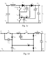
- Fig. 1a is a first example of a three level boost converter in which the present invention is implemented.
- the three level boost converter is composed of an inductor L 1 , two diodes D 1 , and D 2 , three capacitors C 1 , C 2 and C 3 , a first switch S 1 , and a second switch S 2 and of a snubber circuit according to the present invention.
- the snubber circuit is composed of an inductor L SN , two diodes D SN1 and D SN2 and a capacitor C SN and enables the demagnetisation of the inductor L SN during change of conductive/non conductive state of the switch S 2 and enables the slow charge/discharge of the capacitor C SN .
- the three level boost converter has two input terminals 10a and 11a.
- the three level boost converter is connected to a photovoltaic module.
- the present invention is also applicable in any DC power source.
- the input terminal 10a is connected to the positive terminal of the power source and the input terminal 11a is connected to the negative terminal of the power source.
- the capacitor C 1 is connected in parallel with the input terminals 10a and 11a.
- a first terminal of the inductor L 1 is connected to the input terminal 10a and a second terminal of the inductor L 1 is connected to a first terminal of the switch S 1 and to the anode of the diode D 1 .
- the second terminal of the switch S 1 is connected to a first terminal of the inductor L SN of the snubber circuit and to a first terminal of the capacitor C 2 .
- the inductor L SN is connected to a first terminal of the switch S 2 and to the anode of the diode D SN1 .
- the second terminal of the switch S 2 is connected to the input terminal 11a.
- the second terminal of the capacitor C 2 is connected to the cathode of the diode D 1 and to the anode of the diode D 2 .
- the cathode of the diode D 2 is connected to a first output terminal 12a of the three level boost converter.
- the cathode of the diode D SN1 is connected to the anode of the diode D SN2 and to a first terminal of the capacitor C SN .
- the cathode of the diode D SN2 is connected to the anode of the diode D 2 .
- the second terminal of the capacitor C SN is connected to the input terminal 11a and to a second output terminal 13a of the three level boost converter.
- the capacitor C 3 is connected in parallel with the output terminals 12a and 13a.
- Fig. 1b is a second example of a three level boost converter in which the present invention is implemented.
- the three level boost converter is composed of an inductor L 1 , two diodes D 1 and D 2 , three capacitors C 1 , C 2 and C 3 , a first switch S 1 and a second switch S 2 and of a snubber circuit according to the present invention.
- the snubber circuit is composed of an inductor L SN , two diodes D SN1 and D SN2 and a capacitor C SN and enables the demagnetisation of the inductor L SN during change of conductive/non conductive state of the switch S 2 .
- the three level boost converter has two input terminals 10b and 11b.
- the three level boost converter is connected a photovoltaic module.
- the present invention is also applicable in any DC power source.
- the input terminal 10b is connected to the positive terminal of the power source and the input terminal 11b is connected to the negative terminal of the power source.
- the capacitor C 1 is connected in parallel with the input terminals 10b and 11b.
- a first terminal of the inductor L 1 is connected to the input terminal 10b and a second terminal of the inductor L 1 is connected a first terminal of the switch S 1 and to the anode of the diode D 1 .
- the second terminal of the switch S 1 is connected to a first terminal of the switch S 2 , to a first terminal of the capacitor C 2 and to the anode of the diode D SN1 .
- the second terminal of the switch S 2 is connected to the input terminal 11b.
- the second terminal of the capacitor C 2 is connected to the cathode of the diode D 1 and to a first terminal of the inductor L SN .
- the second terminal of the inductor L SN is connected to the anode of the diode D 2 and to the cathode of the diode D SN2 .
- the cathode of the diode D 2 is connected to a first output terminal 12b of the three level boost converter.
- the cathode of the diode D SN1 is connected to the anode of the diode D SN2 and to a first terminal of the capacitor C SN .
- the cathode of the diode D SN2 is connected to the anode of the diode D 2 .
- the second terminal of the capacitor C SN is connected to the input terminal 11b and to a second output terminal 13b of the three level boost converter.
- the capacitor C 3 is connected in parallel with the output terminals 12b and 13b.
- the snubber of Fig. 1b may have second inductor L SN' located at the same location as the inductor L SN of the three level boost converter disclosed in Fig. 1a .
- the second inductor L SN' and the inductor L SN are magnetically coupled.
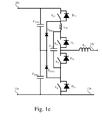
- Fig. 1c is a third example of a boost converter in which the present invention is implemented.
- the boost converter is composed of an inductor L 1 , two diodes D 1 and D 2 , three capacitors C 1 , C 2 and C 3 , a first switch S 11 and a second switch S 12 and of a snubber circuit according to the present invention.
- the snubber circuit is composed of an inductor L SN , two diodes D SN1 and D SN2 and two capacitors C SN11 and C SN12 and enables the demagnetisation of the inductor L SN during change of conductive/non conductive state of the switch S 2 .
- the boost converter has two input terminals 10c and 11c.
- the boost converter is connected to a photovoltaic module.
- the present invention is also applicable in any DC power source.
- the input terminal 10c is connected to the positive terminal of the power source and the input terminal 11c is connected to the negative terminal of the power source.
- the capacitor C 1 is connected in parallel with the input terminals 10c and 11c.
- a first terminal of the inductor L 1 is connected to the input terminal 10c and a second terminal of the inductor L 1 is connected to a first terminal of the switch S 11 and to the anode of the diode D 1 .
- the second terminal of the switch S 11 is connected to a first terminal of the inductor L SN of the snubber circuit and to a first terminal of the capacitor C 2 .
- the inductor L SN is connected to a first terminal of the switch S 22 and to the anode of the diode D SN1 .
- the second terminal of the switch S 22 is connected to the input terminal 11c.
- the second terminal of the capacitor C 2 is connected to the cathode of the diode D 1 and to the anode of the diode D 2 .
- the cathode of the diode D 2 is connected to a first output terminal 12c of the boost converter.
- the cathode of the diode D SN1 is connected to the anode of the diode D SN2 and to a first terminal of the capacitor C SN11 .
- the cathode of the diode D SN12 is connected to the anode of the diode D 2 .
- the second terminal of the capacitor C SN11 is connected to the input terminal 11c and to a second output terminal 13c of the boost converter.
- a first terminal of the capacitor C SN12 is connected to the first terminal of the capacitor C SN11 and to the cathode of the diode D2.
- the snubber of Fig. 1c may have second inductor L SN' located at the same location as the inductor L SN of the three level boost converter disclosed in Fig. 1a .
- the second inductor L SN' and the inductor L SN are magnetically coupled.
- the capacitor C 3 is connected in parallel with the output terminals 12c and 13c.
- Fig. 1d is a fourth example of a buck converter in which the present invention is implemented.
- the buck converter is composed of an inductor L 21 , four diodes D 21 , D 22, D 23 and D 24 , one capacitor C 22 , a first switch S 21 and a second switch S 22 and of a snubber circuit according to the present invention.
- the snubber circuit is composed of an inductor L SN21 , two diodes D SN21 , and D SN22 and two capacitors C SN21 , and C SN22 and enables the demagnetisation of the inductor L SN during change of conductive/non conductive state of the switch S 22 .
- the buck converter has two input terminals 10d and 11d.
- the buck converter is connected to a photovoltaic module.
- the present invention is also applicable in any DC power source.
- the input terminal 10d is connected to the positive terminal of the power source and the input terminal 11d is connected to the negative terminal of the power source.
- a first terminal of the capacitor C SN21 is connected to the input terminal 10d and to a first terminal of the switch S 21 .
- the second terminal of the capacitor C SN21 is connected to the anode of the diode D SN21 , to a first terminal of the capacitor C SN22 and to the cathode of the diode D SN22 .
- the cathode of the diode D SN21 is connected to a first terminal of the inductor L SN and to the second terminal of the switch S 21 .
- the second terminal of the capacitor C SN22 is connected to the input terminal 11d and to the output terminal 13d.
- the anode of diode D SN22 is connected to the cathode of diode D 22 to a first terminal of the capacitor C 22 and to the anode of the diode D 21 .
- the second terminal of the capacitor C 22 is connected to the second terminal of the inductor L SN and to a first terminal of the switch S 22 .
- the second terminal of the switch S 22 is connected to the cathode of the diode D 21 and to a first terminal of the inductor L 21 .
- the second terminal of the inductor L 21 is connected to the output terminal 12d and to a first terminal of the capacitor C 3 .
- the second terminal of the capacitor C 3 is connected to the output terminal 13d.
- the snubber of Fig. 1d may have second inductor L SN' located between the cathode of the diode D22 and the anode of diode D 21
- the second inductor L SN' and the inductor L SN are magnetically coupled.
- Fig. 1e is an example of a bidirectional converter in which the present invention is implemented.
- the bidirectional converter is composed of an inductor L 31 , four diodes D 31 , D 31' , D 32 and D 32' , one capacitor C 32 , a first switch S 31 , a second switch S 32 , a third switch S 31' and a fourth switch S 32' and of a snubber circuit according to the present invention.
- the snubber circuit is composed of an inductor L SN31 , two diodes D SN31 and D SN32 and two capacitors C SN31 and C SN32 and enables the demagnetisation of the inductor L SN during change of conductive/non conductive state of the switch S 32 and S 32 '.
- the bidirectional converter has two terminals 10e and 11e.
- the bidirectional converter is connected to a battery.
- the bidirectional converter has two terminals 12e and 13e.
- the bidirectional converter is connected to an AC/AC converter.
- a first terminal of the capacitor C SN31 is connected to the terminal 10e, to the cathode of the diode D 32' and to a first terminal of the switch S 21 .
- a second terminal of the capacitor C SN31 is connected to a first terminal of the capacitor C sN32 , to the anode of the diode D SN31 and to the cathode of diode D SN32 .
- the second terminal of the switch S 32' is connected to a first terminal of the inductor L SN , to the anode of the diode D 32' and to the cathode of diode D SN31 .
- the second terminal of the inductor L SN is connected to the cathode of the diode D 31' , to a first terminal of the switch S 31' , and to a first terminal of the capacitor C 32 .
- the second terminal of the switch S 31' is connected to the anode of the diode D 31' , to the cathode of the diode D 31 , to a first terminal of the inductor L 31 and to a first terminal of the switch S 31 .
- the second terminal of the switch S 31 is connected to the anode of the diode D 31 , to the cathode of the diode D 32 , to the anode of the diode D SN32 and to a first terminal of the switch S 32 .
- the second terminal of the switch S 32 is connected to the anode of the diode D 32 , to the second terminal of the capacitor C 32 and to the terminals 11e and 13f.
- the snubber circuit protects the switches S 32 and S 32' .
- the second terminal of the inductor L31 is connected to the terminal 12e.
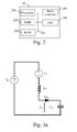
- Fig. 2 represents an example of a device comprising a three level boost converter in which the present invention is implemented.
- the device 20 has, for example, an architecture based on components connected together by a bus 201 and a processor 200 controlled by a program.
- the program enables the control of the switches S 1 and S 2 in order to provide a controlled output voltage V out of the three level boost converter 205 or a controlled input voltage V in .
- the device 20 is, in a variant, implemented under the form of one or several dedicated integrated circuits which execute the same operations as the one executed by the processor 200 as disclosed hereinafter.
- the bus 201 links the processor 200 to a read only memory ROM 202, a random access memory RAM 203, an analog to digital converter ADC 306 and the three level boost converter as the one disclosed in Fig. 1a or 1b or a boost converter as the one disclosed in Fig. 1c or a buck converter as the one disclosed in Fig. 1d or the bidirectional converter as the one disclosed in Fig. 1e .
- the read only memory ROM 202 contains instructions of the program which are transferred, when the device 20 is powered on to the random access memory RAM 203.
- the analog to digital converter 206 is connected to the three level boost converter 205 and converts voltages representative of the output voltage V out into binary information.
- Fig. 3a represents the equivalent electric circuit, during a first phase when a switch of the three level boost converter moves from a conductive state to a non conductive state.
- the current source I L1 is the current provided by the inductor L 1
- the voltage source V C2 is the voltage of the capacitor C 2 .
- the discharge of the inductor L 1 is made through the inductor L SN , the diode D SN1 and the capacitor C SN .
- the voltage V S2 is the voltage between the first and second terminals of the switch S 2 .
- the voltage between the terminals of the diode D SN2 is equal to minus the voltage of the capacitor C 2 and the voltage on capacitor C SN is null.
- the current I L1 flows in capacitor C SN .
- the voltage V D2 on the diode D 2 is equal to:
- C SN value should be replaced, in examples of Figs. 1c and Fig. 1d by the sum of C SN11 and C SN12 values, respectively the sum of C SN11 and C SN12 values.
- L 1 in the example of Fig. 1d is replaced by L 21 .
- the current I L1 is equal to:
- V D2 0.
- Fig. 3b represents the equivalent electric circuit, during a second phase when a switch of the three level boost converter moves from a conductive state to a non conductive state.
- the current source I L1 is the current provided by the inductor L 1
- the voltage source V C2 is the voltage of the capacitor C 2
- the voltage source V out is the voltage at the output of the three level boost converter.
- the discharge of the inductor L 1 is made through the inductor L SN , the diode D SN1 and the capacitor C SN .
- the voltage V S2 is the voltage between the first and second terminals of the switch S 2 .
- the diode D 2 is conductive but the diode D SN2 is still reverse blocked.
- the second phase may stop if L SN is fully discharged before half the resonance period of L SN and C SN .
- ⁇ SN is the angular frequency of the inductor L SN and the capacitor C SN
- I LSN is the current of I LSN .
- ⁇ SN 1 L SN ⁇ C SN .
- V S2 V CSN .
- Fig. 3c represents the equivalent electric circuit, during a third phase when a switch of the three level boost converter moves from a conductive state to a non conductive state.
- the current source I L1 is the current provided by the inductor L 1
- the voltage source V C2 is the voltage of the capacitor C 2
- the voltage source V out is the voltage at the output of the three level boost converter.
- the diode D SN2 becomes conductive.
- the third phase starts if L SN C SN * I L ⁇ 1 ⁇ V C ⁇ 2 .
- the inductor L SN is demagnetized as the voltage -V C2 is applied.
- I LSN t I t c - V C ⁇ 2 L SN ⁇ t - t C
- Figs. 4a and 4b represent current and voltage variations during the first, second and third phases when a switch of the three level boost converter moves from a conductive state to a non conductive state.
- the Fig. 4a represents the evolution of the current I LSN noted 40 and the current I CSN noted 41 during the three phases disclosed in Figs. 3 a to 3c.
- the Fig. 4b represents the evolution of the voltage V CSN noted 45 and the voltage V S2 noted 46 during the three phases disclosed in Figs. 3a to 3c .
- the current I CSN is equal to null value.
- the switch S 2 is turned off, the current I CSN becomes equal to I LSN .
- the capacitor C SN is charged and the voltage V S2 on S 2 grows as the voltage V CSN .
- the diode D 2 is conductive but the diode D SN2 is still reverse blocked.
- the capacitor C 2 value is at least equal to hundred time the capacitor C SN value. Despite the capacitor C 2 is charged, the voltage value of the capacitor C 2 is kept constant by modifying the duty cycle of switch S 1 .
- switches S 1 and S 2 may not be of the same type.
- the switch S1 can operate up to V C2 and those switch S 2 up to V OUT .
- the switching times of the switch S 1 may be much lower than the one of the switch S 2 .
- the switches S 1 and S 2 may be MOSFET or IGBT.
- Fig. 5a represents the equivalent electric circuit, during a fourth phase when a switch of the three level boost converter moves from a non conductive state to a conductive state.
- the current source I L1 is the current provided by the inductor L 1
- the voltage source V C2 is the voltage of the capacitor C 2
- the voltage source V OUT is the voltage of the capacitor C 3 .
- V S ⁇ 2 V out - V C ⁇ 2 - L SN . dI LSN / dt ⁇ 0.
- Fig. 5b represents the equivalent electric circuit, during a fifth phase when a switch of the three level boost converter moves from a non conductive state to a conductive state.
- the current source I L1 is the current provided by the inductor L 1
- the voltage source V C2 is the voltage of the capacitor C 2 .
- the diode D 2 is blocked, the voltage V CSN across the capacitor C SN is higher than the voltage V C2 and tends to discharge through V C2 , L SN and D SN2 .
- the same resonance as disclosed in the second phase occurs and there is no dissipative energy transfer.
- the snubber capacitor C SN must discharge before T SN /2 where T SN is the period of the resonant circuit composed of C SN and L SN which means that V out ⁇ V C 2 *2
- Fig. 5c represents the equivalent electric circuit, during a sixth phase, of the discharge of an inductor of the three level boost converter when a switch of the three level boost converter moves from a non conductive state to a conductive state.
- the current source I L1 is the current provided by the inductor L 1
- the voltage source V C2 is the voltage of the capacitor C 2
- the voltage source V OUT is the voltage of the capacitor C 3 .
- a positive current keeps flowing in the diode D SN2 , the diode D SN1 becomes conductive when the voltage V CSN reaches null value.
- I LSN t I L ⁇ 1 t c ⁇ - V C ⁇ 2 L CSN * t - t c ⁇
- Figs. 6 represent current and voltage variations during the fourth, fifth and sixth phases when a switch of the three level boost converter moves from a non conductive state to a conductive state.
- the Fig. 6a represents the evolution of the current I LSN noted 60 and the current I CSN noted 61 during the three phases disclosed in Figs. 5a to 5c .
- the Fig. 6b represents the evolution of the voltage V CSN noted 65 and the voltage V S2 noted 66 during the three phases disclosed in Figs. 5a to 5c .
- V S ⁇ 2 V out - V C ⁇ 2 - L SN . dI LSN / dt ⁇ 0.
- the fifth phase starts.
- the diode D 2 is blocked, the voltage V CSN across the capacitor C SN is higher than the voltage V C2 and tends to discharge through V C2 , L SN and D SN2 .
- the same resonance as disclosed in the second phase occurs and there is no dissipative energy transfer.
- V CSN V C ⁇ 2 + V out - V C ⁇ 2 * cos ⁇ SN .
- the snubber capacitor C SN must discharge before T SN /2 where T SN is the period of the resonant circuit composed of C SN and L SN which means that V OUT ⁇ V C 2 *2
- the current source I L1 is the current provided by the inductor L 1
- the voltage source V C2 is the voltage of the capacitor C 2
- the voltage source V OUT is the voltage of the capacitor C 3 .
- a positive current keeps flowing in the diode D SN2 , the diode D SN1 becomes conductive when the voltage V CSN reaches null value.
- I LSN t I L ⁇ 1 t c ⁇ - V C ⁇ 2 L CSN * t - t c ⁇
Landscapes
- Engineering & Computer Science (AREA)
- Power Engineering (AREA)
- Dc-Dc Converters (AREA)
Abstract
Description
- The present invention relates generally to a converter composed of at least a first and a second switches, a first inductor, a first capacitor and at least two diodes and a snubber circuit which protects the second switch.
- A photovoltaic cell directly converts solar energy into electrical energy. The electrical energy produced by the photovoltaic cell can be extracted over time and used in the form of electric power. The direct electric power generated by photovoltaic cell is provided to conversion devices like DC-DC converter circuits and to DC/AC inverter circuits.
- However, the current-voltage droop characteristics of photovoltaic cells cause the output power to change nonlinearly with the current drawn from photovoltaic cells. The power-voltage curve changes according to climatic variations like light irradiance levels and operation temperatures.
- The near optimal point at which to operate photovoltaic arrays is at or near the region of the current-voltage curve where power is greatest. This point is denominated as the Maximum Power Point (MPP).
- It is important to operate the photovoltaic cells around the MPP to optimize their power generation efficiency.
- As the power-voltage curve changes according to climatic variations, the MPP also changes according to climatic variations.
- It is then necessary to be able to identify the MPP anytime.
- For that, the duty cycle of switches of DC-DC converter circuit is modified in order to adapt the DC-DC converter to any input voltage and/or current.
- As DC-DC converters comprise parasitic or stray inductors and switches, sudden interruption of current flow leading to a sharp rise in voltage across the switching device, in accordance with Faraday's law. This transient can be a source of electromagnetic interference. Additionally, if the voltage generated across the device is beyond what the device is intended to withstand, it may damage or destroy it. A snubber provides a short-term alternative current path around the current switching device so that the inductive elements may be discharged more safely and quietly.
- To that end, the present invention concerns a DC-DC converter composed of at least a first and a second switches, a first inductor, a first capacitor and at least two diodes and a snubber circuit which protects the second switch, characterized in that the snubber circuit is composed of a second inductor, at least a second capacitor and a third and a fourth diodes and in that the discharge of the second inductor is performed through the second capacitor during a time period which is at most half the period of the resonant circuit composed of the second capacitor and the second inductor and in the first capacitor after the time period.
- Thus, the sudden interruption of current flow leads to a sharp rise in voltage across the second switch is avoided.
- According to a particular feature, the DC-DC converter is a three level boost converter.
- According to a first mode of realization, a first terminal of the second inductor is connected to a terminal of the first switch and to a terminal of the first capacitor, a second terminal of the second inductor is connected to the anode of the third diode and to a first terminal of the second switch, the cathode of the third diode is connected to the anode of the fourth diode and to a terminal of the second capacitor, the second terminal of the second capacitor is connected to an input terminal of the DC-DC converter and to the second terminal of the second switch, the cathode of the fourth diode is connected to the second terminal of the first capacitor.
- Thus, the sudden interruption of current flow leads to a sharp rise in voltage across the second switch is avoided.
- According to a second mode of realization, a terminal of the first switch is connected to a terminal of the first capacitor, to the anode of the third diode and to a first terminal of the second switch, the cathode of the third diode is connected to the anode of the fourth diode and to a terminal of the second capacitor, the second terminal of the second capacitor is connected to an input terminal of the DC-DC converter and to the second terminal of the second switch, a second terminal of the first capacitor is connected to a first terminal of the second inductor and the second terminal of the inductor is connected to the cathode of the fourth diode.
- Thus, the sudden interruption of current flow leads to a sharp rise in voltage across the second switch is avoided.
- According to a particular feature, the DC-DC converter is a boost converter.
- According to a particular feature, a first terminal of the second switch is connected to a terminal of the first capacitor and to the anode of the third diode, the cathode of the third diode is connected to the anode of the fourth diode and to a first terminal of the second capacitor, the second terminal of the second capacitor is connected to an input terminal of the DC-DC converter and to the second terminal of the second switch, the first terminal of the second inductor is connected to a first terminal of the second capacitor and the cathode of the fourth diode is connected to the second terminal of the second inductor.
- Thus, the sudden interruption of current flow leads to a sharp rise in voltage across the second switch is avoided.
- According to a particular feature, the snubber circuit further comprises another capacitor of which a first terminal is connected to the anode of the fourth diode and a second is connected to the anode of the second diode.
- According to a particular feature, the DC-DC converter is a buck converter.
- According to a particular feature, a first terminal of the first switch is connected to a first input of the DC-DC converter, the anode of the third diode is connected to the cathode of the fourth diode, to a first terminal of the third capacitor, the cathode of the third diode is connected to a first terminal of the second inductor and to a second terminal of the first switch, the anode of the third diode is connected to the anode of the fourth diode and to the cathode of the second diode and to a first terminal of the second capacitor, the second terminal of the second capacitor is connected to a second terminal of the second inductor and to a first terminal of the second switch, the second terminal of the second switch is connected to the cathode of the second diode and to a first terminal of the first inductor, the second terminal of the first inductor is connected to a first output terminal of the DC-DC converter, the second terminal of the fourth capacitor is connected to a second input and output terminals of the DC-DC converter and to the anode of the second diode.
- Thus, the sudden interruption of current flow leads to a sharp rise in voltage across the second switch is avoided.
- According to a particular feature, the snubber circuit further comprises another capacitor of which a first terminal is connected to the anode of the third diode and a second terminal is connected to the first terminal of the first switch.
- According to a particular feature, the converter is a bidirectional converter which further comprises a third and a fourth switches, a third and a fourth diodes, the snubber circuit further protects the fourth switch and the snubber circuit further comprises a third capacitor.
- The characteristics of the invention will emerge more clearly from a reading of the following description of an example embodiment, the said description being produced with reference to the accompanying drawings, among which :
-
Fig. 1a is a first example of a three level boost converter in which the present invention is implemented; -
Fig. 1b is a second example of a three level boost converter in which the present invention is implemented; -
Fig. 1c is a third example of a boost converter in which the present invention is implemented; -
Fig. 1d is a fourth example of a buck converter in which the present invention is implemented; -
Fig. 1e is an example of a bidirectional converter in which the present invention is implemented; -
Fig. 2 represents an example of a device comprising a three level converter or a three level bidirectional converter in which the present invention is implemented; -
Fig. 3a represents the equivalent electric circuit, during a first phase when a switch of the three level boost converter moves from a conductive state to a non conductive state; -
Fig. 3b represents the equivalent electric circuit, during a second phase when a switch of the three level boost converter moves from a conductive state to a non conductive state; -
Fig. 3c represents the equivalent electric circuit, during a third phase when a switch of the three level boost converter moves from a conductive state to a non conductive state; -
Figs. 4a and 4b represent current and voltage variations during the first, second and third phases when a switch of the three level boost converter moves from a conductive state to a non conductive state; -
Fig. 5a represents the equivalent electric circuit, during a fourth phase when a switch of the three level boost converter moves from a non conductive state to a conductive state; -
Fig. 5b represents the equivalent electric circuit, during a fifth phase when a switch of the three level boost converter moves from a non conductive state to a conductive state; -
Fig. 5c represents the equivalent electric circuit, during a sixth phase when a switch of the three level boost converter moves from a non conductive state to a conductive state; -
Figs. 6 represent current and voltage variations during the fourth, fifth and sixth phases when a switch of the three level boost converter moves from a non conductive state to a conductive state. -
Fig. 1a is a first example of a three level boost converter in which the present invention is implemented. - The three level boost converter is composed of an inductor L1, two diodes D1, and D2, three capacitors C1, C2 and C3, a first switch S1, and a second switch S2 and of a snubber circuit according to the present invention.
- The snubber circuit is composed of an inductor LSN, two diodes DSN1 and DSN2 and a capacitor CSN and enables the demagnetisation of the inductor LSN during change of conductive/non conductive state of the switch S2 and enables the slow charge/discharge of the capacitor CSN.
- The three level boost converter has two
input terminals - For example, the
input terminal 10a is connected to the positive terminal of the power source and theinput terminal 11a is connected to the negative terminal of the power source. - The capacitor C1 is connected in parallel with the
input terminals - A first terminal of the inductor L1 is connected to the
input terminal 10a and a second terminal of the inductor L1 is connected to a first terminal of the switch S1 and to the anode of the diode D1. - The second terminal of the switch S1 is connected to a first terminal of the inductor LSN of the snubber circuit and to a first terminal of the capacitor C2.
- The inductor LSN is connected to a first terminal of the switch S2 and to the anode of the diode DSN1. The second terminal of the switch S2 is connected to the
input terminal 11a. - The second terminal of the capacitor C2 is connected to the cathode of the diode D1 and to the anode of the diode D2 .
- The cathode of the diode D2 is connected to a
first output terminal 12a of the three level boost converter. - The cathode of the diode DSN1 is connected to the anode of the diode DSN2 and to a first terminal of the capacitor CSN.
- The cathode of the diode DSN2 is connected to the anode of the diode D2.
- The second terminal of the capacitor CSN is connected to the
input terminal 11a and to asecond output terminal 13a of the three level boost converter. - The capacitor C3 is connected in parallel with the
output terminals -
Fig. 1b is a second example of a three level boost converter in which the present invention is implemented. - The three level boost converter is composed of an inductor L1, two diodes D1 and D2, three capacitors C1, C2 and C3, a first switch S1 and a second switch S2 and of a snubber circuit according to the present invention.
- The snubber circuit is composed of an inductor LSN, two diodes DSN1 and DSN2 and a capacitor CSN and enables the demagnetisation of the inductor LSN during change of conductive/non conductive state of the switch S2.
- The three level boost converter has two
input terminals - For example, the
input terminal 10b is connected to the positive terminal of the power source and theinput terminal 11b is connected to the negative terminal of the power source. - The capacitor C1 is connected in parallel with the
input terminals - A first terminal of the inductor L1 is connected to the
input terminal 10b and a second terminal of the inductor L1 is connected a first terminal of the switch S1 and to the anode of the diode D1. - The second terminal of the switch S1 is connected to a first terminal of the switch S2, to a first terminal of the capacitor C2 and to the anode of the diode DSN1. The second terminal of the switch S2 is connected to the
input terminal 11b. - The second terminal of the capacitor C2 is connected to the cathode of the diode D1 and to a first terminal of the inductor LSN.
- The second terminal of the inductor LSN is connected to the anode of the diode D2 and to the cathode of the diode DSN2.
- The cathode of the diode D2 is connected to a
first output terminal 12b of the three level boost converter. - The cathode of the diode DSN1 is connected to the anode of the diode DSN2 and to a first terminal of the capacitor CSN.
- The cathode of the diode DSN2 is connected to the anode of the diode D2.
- The second terminal of the capacitor CSN is connected to the
input terminal 11b and to asecond output terminal 13b of the three level boost converter. - The capacitor C3 is connected in parallel with the
output terminals - It has to noted here that in a variant of realization, the snubber of
Fig. 1b may have second inductor LSN' located at the same location as the inductor LSN of the three level boost converter disclosed inFig. 1a . In such variant of realization, the second inductor LSN' and the inductor LSN are magnetically coupled. -
Fig. 1c is a third example of a boost converter in which the present invention is implemented. - The boost converter is composed of an inductor L1, two diodes D1 and D2, three capacitors C1, C2 and C3, a first switch S11 and a second switch S12 and of a snubber circuit according to the present invention.
- The snubber circuit is composed of an inductor LSN, two diodes DSN1 and DSN2 and two capacitors CSN11 and CSN12 and enables the demagnetisation of the inductor LSN during change of conductive/non conductive state of the switch S2.
- The boost converter has two
input terminals - For example, the
input terminal 10c is connected to the positive terminal of the power source and theinput terminal 11c is connected to the negative terminal of the power source. - The capacitor C1 is connected in parallel with the
input terminals - A first terminal of the inductor L1 is connected to the
input terminal 10c and a second terminal of the inductor L1 is connected to a first terminal of the switch S11 and to the anode of the diode D1. - The second terminal of the switch S11 is connected to a first terminal of the inductor LSN of the snubber circuit and to a first terminal of the capacitor C2.
- The inductor LSN is connected to a first terminal of the switch S22 and to the anode of the diode DSN1. The second terminal of the switch S22 is connected to the
input terminal 11c. - The second terminal of the capacitor C2 is connected to the cathode of the diode D1 and to the anode of the diode D2.
- The cathode of the diode D2 is connected to a
first output terminal 12c of the boost converter. - The cathode of the diode DSN1 is connected to the anode of the diode DSN2 and to a first terminal of the capacitor CSN11.
- The cathode of the diode DSN12 is connected to the anode of the diode D2.
- The second terminal of the capacitor CSN11 is connected to the
input terminal 11c and to asecond output terminal 13c of the boost converter. - A first terminal of the capacitor CSN12 is connected to the first terminal of the capacitor CSN11 and to the cathode of the diode D2.
- It has to be noted here that the behaviour of the capacitors CSN11 and CSN12 are complementary. When the capacitor CSN11 charges, the capacitor CSN12 discharges and when the capacitor CSN11 discharges, the capacitor CSN12 charges.
- It has to be noted here that in a variant of realization, the snubber of
Fig. 1c may have second inductor LSN' located at the same location as the inductor LSN of the three level boost converter disclosed inFig. 1a . In such variant of realization, the second inductor LSN' and the inductor LSN are magnetically coupled. - The capacitor C3 is connected in parallel with the
output terminals -
Fig. 1d is a fourth example of a buck converter in which the present invention is implemented. - The buck converter is composed of an inductor L21, four diodes D21, D22, D23 and D24, one capacitor C22, a first switch S21 and a second switch S22 and of a snubber circuit according to the present invention.
- The snubber circuit is composed of an inductor LSN21, two diodes DSN21, and DSN22 and two capacitors CSN21, and CSN22 and enables the demagnetisation of the inductor LSN during change of conductive/non conductive state of the switch S22.
- The buck converter has two
input terminals 10d and 11d. For example the buck converter is connected to a photovoltaic module. The present invention is also applicable in any DC power source. - For example, the
input terminal 10d is connected to the positive terminal of the power source and the input terminal 11d is connected to the negative terminal of the power source. - A first terminal of the capacitor CSN21 is connected to the
input terminal 10d and to a first terminal of the switch S21. - The second terminal of the capacitor CSN21 is connected to the anode of the diode DSN21, to a first terminal of the capacitor CSN22 and to the cathode of the diode DSN22.
- The cathode of the diode DSN21 is connected to a first terminal of the inductor LSN and to the second terminal of the switch S21.
- The second terminal of the capacitor CSN22 is connected to the input terminal 11d and to the
output terminal 13d. - The anode of diode DSN22 is connected to the cathode of diode D22 to a first terminal of the capacitor C22 and to the anode of the diode D21.
- The second terminal of the capacitor C22 is connected to the second terminal of the inductor LSN and to a first terminal of the switch S22.
- The second terminal of the switch S22 is connected to the cathode of the diode D21 and to a first terminal of the inductor L21.
- The second terminal of the inductor L21 is connected to the
output terminal 12d and to a first terminal of the capacitor C3. - The second terminal of the capacitor C3 is connected to the
output terminal 13d. - It has to be noted here that the behaviours of the capacitors CSN11 and CSN12 are complementary. When the capacitor CSN11 charges, the capacitor CSN12 discharges and when the capacitor CSN11 discharges, the capacitor CSN12 charges.
- It has to be noted here that in a variant of realization, the snubber of
Fig. 1d may have second inductor LSN' located between the cathode of the diode D22 and the anode of diode D21 In such variant of realization, the second inductor LSN' and the inductor LSN are magnetically coupled. -
Fig. 1e is an example of a bidirectional converter in which the present invention is implemented. - The bidirectional converter is composed of an inductor L31, four diodes D31, D31', D32 and D32', one capacitor C32, a first switch S31, a second switch S32, a third switch S31' and a fourth switch S32' and of a snubber circuit according to the present invention.
- The snubber circuit is composed of an inductor LSN31, two diodes DSN31 and DSN32 and two capacitors CSN31 and CSN32 and enables the demagnetisation of the inductor LSN during change of conductive/non conductive state of the switch S32 and S32'.
- The bidirectional converter has two
terminals - The bidirectional converter has two
terminals - A first terminal of the capacitor CSN31 is connected to the terminal 10e, to the cathode of the diode D32' and to a first terminal of the switch S21.
- A second terminal of the capacitor CSN31 is connected to a first terminal of the capacitor CsN32, to the anode of the diode DSN31 and to the cathode of diode DSN32.
- The second terminal of the switch S32' is connected to a first terminal of the inductor LSN, to the anode of the diode D32' and to the cathode of diode DSN31.
- The second terminal of the inductor LSN is connected to the cathode of the diode D31', to a first terminal of the switch S31', and to a first terminal of the capacitor C32.
- The second terminal of the switch S31' is connected to the anode of the diode D31', to the cathode of the diode D31, to a first terminal of the inductor L31 and to a first terminal of the switch S31.
- The second terminal of the switch S31 is connected to the anode of the diode D31, to the cathode of the diode D32, to the anode of the diode DSN32 and to a first terminal of the switch S32.
- The second terminal of the switch S32 is connected to the anode of the diode D32, to the second terminal of the capacitor C32 and to the
terminals 11e and 13f. - The snubber circuit protects the switches S32 and S32'.
- The second terminal of the inductor L31 is connected to the terminal 12e.
-
Fig. 2 represents an example of a device comprising a three level boost converter in which the present invention is implemented. - The
device 20 has, for example, an architecture based on components connected together by abus 201 and aprocessor 200 controlled by a program. The program enables the control of the switches S1 and S2 in order to provide a controlled output voltage Vout of the threelevel boost converter 205 or a controlled input voltage Vin. - It has to be noted here that the
device 20 is, in a variant, implemented under the form of one or several dedicated integrated circuits which execute the same operations as the one executed by theprocessor 200 as disclosed hereinafter. - The
bus 201 links theprocessor 200 to a read onlymemory ROM 202, a randomaccess memory RAM 203, an analog to digital converter ADC 306 and the three level boost converter as the one disclosed inFig. 1a or 1b or a boost converter as the one disclosed inFig. 1c or a buck converter as the one disclosed inFig. 1d or the bidirectional converter as the one disclosed inFig. 1e . - The read only
memory ROM 202 contains instructions of the program which are transferred, when thedevice 20 is powered on to the randomaccess memory RAM 203. - The analog to
digital converter 206 is connected to the threelevel boost converter 205 and converts voltages representative of the output voltage Vout into binary information. -
Fig. 3a represents the equivalent electric circuit, during a first phase when a switch of the three level boost converter moves from a conductive state to a non conductive state. - The equivalent circuits given in
Fig. 3 are taken for the first example given inFig. 1a . Similar equivalent circuits may be easily derived from the teaching ofFigs. 3 for the examples given inFigs. 1b ,1c and 1d . - It has to be noted here that the equivalent circuits disclosed in
Figs. 3 and5 are given when the duty cycle of the switch S2 is equal or upper than ½. - The current source IL1 is the current provided by the inductor L1, the voltage source VC2 is the voltage of the capacitor C2. The discharge of the inductor L1 is made through the inductor LSN, the diode DSN1 and the capacitor CSN. The voltage VS2 is the voltage between the first and second terminals of the switch S2.
- When the switch S2 changes from a conductive state to a non conductive state, and as the freewheeling diode D2 remains reverse blocked, the current IL1 of the inductor L1 is constant and the capacitor CSN is charged.
- The voltage between the terminals of the diode DSN2 is equal to minus the voltage of the capacitor C2 and the voltage on capacitor CSN is null.
- The current IL1 flows in capacitor CSN.
- The voltage VD2 on the diode D2 is equal to:
- VD2= -VC2 - Vout - VCSN, where VCSN is the voltage on the capacitor CSN.
- It has to be noted here that CSN value should be replaced, in examples of
Figs. 1c and Fig. 1d by the sum of CSN11 and CSN12 values, respectively the sum of CSN11 and CSN12 values. - It has also to be noted here that L1, in the example of
Fig. 1d is replaced by L21. - The current IL1 is equal to:
- IL1= CSN*dVCSN/dt, then VCSN(t)= IL1.t/CSN, where t is the time and d the derivative.
- When CSN reaches VD2-Vout, then VD2=0.
- The first phase ends when t=CSN*(VC2-Vout)/IL1.
-
Fig. 3b represents the equivalent electric circuit, during a second phase when a switch of the three level boost converter moves from a conductive state to a non conductive state. - The current source IL1 is the current provided by the inductor L1, the voltage source VC2 is the voltage of the capacitor C2 and the voltage source Vout is the voltage at the output of the three level boost converter. The discharge of the inductor L1 is made through the inductor LSN, the diode DSN1 and the capacitor CSN. The voltage VS2 is the voltage between the first and second terminals of the switch S2.
- Once the first phase ends, the diode D2 is conductive but the diode DSN2 is still reverse blocked. The inductor LSN and the capacitor CSN oscillate up to the diode DSN2 becomes conductive. However, the second phase may stop if LSN is fully discharged before half the resonance period of LSN and CSN.

- Where ω SN is the angular frequency of the inductor LSN and the capacitor CSN, ILSN is the current of ILSN.

- The voltage across the switch S2 is then VS2=VCSN.
- Once

-
Fig. 3c represents the equivalent electric circuit, during a third phase when a switch of the three level boost converter moves from a conductive state to a non conductive state. - The current source IL1 is the current provided by the inductor L1, the voltage source VC2 is the voltage of the capacitor C2 and the voltage source Vout is the voltage at the output of the three level boost converter. The diode DSN2 becomes conductive.
- The third phase starts if

- The inductor LSN is demagnetized as the voltage -VC2 is applied.

- The voltage across the switch S2 is then VS2 = Vout.
- Then, when the third phase ends up, the diode DSN1 is reverse biased and

-
Figs. 4a and 4b represent current and voltage variations during the first, second and third phases when a switch of the three level boost converter moves from a conductive state to a non conductive state. - The
Fig. 4a represents the evolution of the current ILSN noted 40 and the current ICSN noted 41 during the three phases disclosed inFigs. 3 a to 3c. - The
Fig. 4b represents the evolution of the voltage VCSN noted 45 and the voltage VS2 noted 46 during the three phases disclosed inFigs. 3a to 3c . - Prior the first phase, noted 42 in
Figs. 4 , the current ICSN is equal to null value. When the switch S2 is turned off, the current ICSN becomes equal to ILSN. The capacitor CSN is charged and the voltage VS2 on S2 grows as the voltage VCSN. The first phase ends when t=CSN*(VC2-Vout)/IL1. - During the second phase noted 43 in
Figs. 4 , the diode D2 is conductive but the diode DSN2 is still reverse blocked. The inductor LSN and the capacitor CSN oscillate up to the diode DSN2 becomes conductive. The current ICSN and ILSN decrease. - The voltage VS2 as the voltage VCSN reaches the voltage value of Vout.
- Once

Figs. 4 starts. The current ILSN starts to flow into the capacitor C2, the voltage VS2 becomes equal to Vout -VC2 and the voltage VC2 becomes equal to Vout. - It has to be noted here that the capacitor C2 value is at least equal to hundred time the capacitor CSN value. Despite the capacitor C2 is charged, the voltage value of the capacitor C2 is kept constant by modifying the duty cycle of switch S1.
- It has to be noted here that the switches S1 and S2 may not be of the same type. For example the switch S1 can operate up to VC2 and those switch S2 up to VOUT. The switching times of the switch S1 may be much lower than the one of the switch S2.
- For example, the switches S1 and S2 may be MOSFET or IGBT.
-
Fig. 5a represents the equivalent electric circuit, during a fourth phase when a switch of the three level boost converter moves from a non conductive state to a conductive state. - The current source IL1 is the current provided by the inductor L1, the voltage source VC2 is the voltage of the capacitor C2 and the voltage source VOUT is the voltage of the capacitor C3.
- The switch S2 is switched in conductive state, which corresponds to inductive turn ON effect:

- Then, LSN . ILSN /dt = Vout-VC2 ≥ 0, the inductor LSN is then magnetized.
- When IL1 flows in the switch S2 instead of the diode D2, D2 is reverse blocked and voltage across can evolve depending on other elements.
- The duration of the fourth phase equals : Δta = LSN .IL1 / (Vout - VC2).
-
Fig. 5b represents the equivalent electric circuit, during a fifth phase when a switch of the three level boost converter moves from a non conductive state to a conductive state. - The current source IL1 is the current provided by the inductor L1, the voltage source VC2 is the voltage of the capacitor C2.
- Once the fourth phase ends, the diode D2 is blocked, the voltage VCSN across the capacitor CSN is higher than the voltage VC2 and tends to discharge through VC2, LSN and DSN2. The same resonance as disclosed in the second phase occurs and there is no dissipative energy transfer.
- Considering initial conditions :
- VCSN = Vout and ILSN = IL1.
- The snubber capacitor CSN must discharge before TSN /2 where TSN is the period of the resonant circuit composed of CSN and LSN which means that V out ≥ V C2 *2
- Once VCSN=0, the fifth phase ends and the sixth phase starts.
-
Fig. 5c represents the equivalent electric circuit, during a sixth phase, of the discharge of an inductor of the three level boost converter when a switch of the three level boost converter moves from a non conductive state to a conductive state. - The current source IL1 is the current provided by the inductor L1, the voltage source VC2 is the voltage of the capacitor C2 and the voltage source VOUT is the voltage of the capacitor C3.
- A positive current keeps flowing in the diode DSN2, the diode DSN1 becomes conductive when the voltage VCSN reaches null value.
- The sixth phase starts before :

- The inductor LSN is then demagnetised :

-
Figs. 6 represent current and voltage variations during the fourth, fifth and sixth phases when a switch of the three level boost converter moves from a non conductive state to a conductive state. - The
Fig. 6a represents the evolution of the current ILSN noted 60 and the current ICSN noted 61 during the three phases disclosed inFigs. 5a to 5c . - The
Fig. 6b represents the evolution of the voltage VCSN noted 65 and the voltage VS2 noted 66 during the three phases disclosed inFigs. 5a to 5c . - Prior the fourth phase, noted 62 in
Figs. 6 , the switch S2 moves from a non conductive step to a conductive state.
- Then, LSN . ILSN /dt = Vout-VC2 ≥ 0, the inductor LSN is then magnetized.
- When IL1 flows in the switch S2 instead of the diode D2, D2 is reverse blocked and voltage across can evolve depending on other elements.
- The duration of the fourth phase equals : Δta = LSN .IL1 / (Vout - VC2).
- Once the fourth phase noted 63 in
Figs. 6 ends, the fifth phase starts. The diode D2 is blocked, the voltage VCSN across the capacitor CSN is higher than the voltage VC2 and tends to discharge through VC2, LSN and DSN2. The same resonance as disclosed in the second phase occurs and there is no dissipative energy transfer. - Considering initial conditions :


- The snubber capacitor CSN must discharge before TSN /2 where TSN is the period of the resonant circuit composed of CSN and LSN which means that VOUT ≥ V C2 *2
- Once VCSN=0, the fifth phase ends and the sixth phase starts.
- The current source IL1 is the current provided by the inductor L1, the voltage source VC2 is the voltage of the capacitor C2 and the voltage source VOUT is the voltage of the capacitor C3.
- A positive current keeps flowing in the diode DSN2, the diode DSN1 becomes conductive when the voltage VCSN reaches null value.
- The sixth phase starts before :

- The inductor LSN is then demagnetised :

- Naturally, many modifications can be made to the embodiments of the invention described above without departing from the scope of the present invention.


Claims (12)
- Converter composed of at least a first and a second switches, a first inductor, a first capacitor and at least two diodes and a snubber circuit which protects the second switch, characterized in that the snubber circuit is composed of a second inductor, a second capacitor and a third and a fourth diodes and in that the discharge of the second inductor is performed through the second capacitor during a time period which is at most half the period of the resonant circuit composed of the second capacitor and the second inductor and in the first capacitor after the time period.
- Converter according to claim 1, characterized in that the converter is a DC-DC converter.
- Converter according to claim 2, characterized in that the converter is a three level buck or boost converter.
- Converter according to claim 3, characterized in that a first terminal of the second inductor is connected to a terminal of the first switch and to a terminal of the first capacitor, a second terminal of the second inductor is connected to the anode of the third diode and to a first terminal of the second switch, the cathode of the third diode is connected to the anode of the fourth diode and to a terminal of the second capacitor, the second terminal of the second capacitor is connected to an input terminal of the DC-DC converter and to the second terminal of the second switch, the cathode of the fourth diode is connected to the second terminal of the first capacitor.
- Converter according to claim 3, characterized in that a terminal of the first switch is connected to a terminal of the first capacitor, to the anode of the third diode and to a first terminal of the second switch, the cathode of the third diode is connected to the anode of the fourth diode and to a terminal of the second capacitor, the second terminal of the second capacitor is connected to an input terminal of the DC-DC converter and to the second terminal of the second switch, a second terminal of the first capacitor is connected to a first terminal of the second inductor and the second terminal of the inductor is connected to the cathode of the fourth diode.
- Converter according to claim 2, characterized in that the converter is a boost converter.
- Converter according to claim 6, characterized in that a first terminal of the second switch is connected to a terminal of the first capacitor and to the anode of the third diode, the cathode of the third diode is connected to the anode of the fourth diode and to a first terminal of the second capacitor, the second terminal of the second capacitor is connected to an input terminal of the converter and to the second terminal of the second switch, the first terminal of the second inductor is connected to a first terminal of the second capacitor and the cathode of the fourth diode is connected to the second terminal of the second inductor.
- Converter according to claim 7, characterized in that the snubber circuit further comprises another capacitor of which a first terminal is connected to the anode of the fourth diode and a second is connected to the anode of the second diode.
- Converter according to claim 2, characterized in that the converter is a buck converter.
- Converter according to claim 9, characterized in that a first terminal of the first switch is connected to a first input of the converter, the anode of the third diode is connected to the cathode of the fourth diode, to a first terminal of the third capacitor, the cathode of the third diode is connected to a first terminal of the second inductor and to a second terminal of the first switch, the anode of the third diode is connected to the anode of the fourth diode and to the cathode of the second diode and to a first terminal of the second capacitor, the second terminal of the second capacitor is connected to a second terminal of the second inductor and to a first terminal of the second switch, the second terminal of the second switch is connected to the cathode of the second diode and to a first terminal of the first inductor, the second terminal of the first inductor is connected to a first output terminal of the DC-DC converter, the second terminal of the fourth capacitor is connected to a second input and output terminals of the converter and to the anode of the second diode.
- Converter according to claim 7, characterized in that the snubber circuit further comprises another capacitor of which a first terminal is connected to the anode of the third diode and a second terminal is connected to the first terminal of the first switch.
- Converter according to claim 1, characterized in that the converter is a bidirectional converter which further comprises a third and a fourth switch, a third and a fourth diodes, the snubber circuit further protects the fourth switch and the snubber circuit further comprises a third capacitor.
Priority Applications (2)
| Application Number | Priority Date | Filing Date | Title |
|---|---|---|---|
| EP13160435.7A EP2782235A1 (en) | 2013-03-21 | 2013-03-21 | Converter composed of at least a first and a second switches and a snubber circuit which protects the second switch |
| JP2014015822A JP6395387B2 (en) | 2013-03-21 | 2014-01-30 | converter |
Applications Claiming Priority (1)
| Application Number | Priority Date | Filing Date | Title |
|---|---|---|---|
| EP13160435.7A EP2782235A1 (en) | 2013-03-21 | 2013-03-21 | Converter composed of at least a first and a second switches and a snubber circuit which protects the second switch |
Publications (1)
| Publication Number | Publication Date |
|---|---|
| EP2782235A1 true EP2782235A1 (en) | 2014-09-24 |
Family
ID=47913190
Family Applications (1)
| Application Number | Title | Priority Date | Filing Date |
|---|---|---|---|
| EP13160435.7A Withdrawn EP2782235A1 (en) | 2013-03-21 | 2013-03-21 | Converter composed of at least a first and a second switches and a snubber circuit which protects the second switch |
Country Status (2)
| Country | Link |
|---|---|
| EP (1) | EP2782235A1 (en) |
| JP (1) | JP6395387B2 (en) |
Cited By (15)
| Publication number | Priority date | Publication date | Assignee | Title |
|---|---|---|---|---|
| AT516328A1 (en) * | 2014-09-15 | 2016-04-15 | Felix Dipl Ing Dr Himmelstoss | High-low converter with reduced duty cycle for one-quadrant operation |
| CN106160549A (en) * | 2015-04-24 | 2016-11-23 | 郑州大学 | A kind of three-phase inverter using overlapping dual power supply |
| CN107070215A (en) * | 2017-04-12 | 2017-08-18 | 特变电工西安电气科技有限公司 | A kind of three level boost system with one power and its control method |
| CN105576971B (en) * | 2016-03-18 | 2018-06-19 | 南通大学 | Input, the continuous three level Buck converters of output current |
| CN108988635A (en) * | 2018-09-13 | 2018-12-11 | 阳光电源股份有限公司 | A kind of more level Boost converters, inversion system and control method |
| CN110165888A (en) * | 2019-06-11 | 2019-08-23 | 阳光电源股份有限公司 | Three level Boost circuits, multiple-channel output parallel system |
| KR102045156B1 (en) * | 2018-11-12 | 2019-11-14 | 서울과학기술대학교 산학협력단 | Active snubber cell for soft-switched and boost converter including the same |
| AT521410A1 (en) * | 2018-07-02 | 2020-01-15 | Fachhochschule Technikum Wien | Buck converter with low switching losses |
| AT521475A4 (en) * | 2018-11-26 | 2020-02-15 | Fachhochschule Technikum Wien | Combined D, 2D converter |
| WO2021027468A1 (en) * | 2019-08-15 | 2021-02-18 | 华为技术有限公司 | Dc-dc converter circuit |
| CN112701913A (en) * | 2019-10-22 | 2021-04-23 | 阳光电源股份有限公司 | Boost power conversion circuit and control method and application device thereof |
| CN112769342A (en) * | 2021-01-07 | 2021-05-07 | 济南新吉纳远程测控股份有限公司 | Wide-range AC-DC power supply conversion system and method of drilling wireless while-drilling instrument |
| WO2021109538A1 (en) * | 2019-12-05 | 2021-06-10 | 毛昭祺 | Dc-dc circuit applicable to high-voltage input |
| CN116893703A (en) * | 2022-03-29 | 2023-10-17 | 本田技研工业株式会社 | AC generating circuit and heating device |
| WO2025102427A1 (en) * | 2023-11-13 | 2025-05-22 | 阳光电源股份有限公司 | Suspension capacitor three-level boost converter and control method |
Families Citing this family (2)
| Publication number | Priority date | Publication date | Assignee | Title |
|---|---|---|---|---|
| US10461640B2 (en) * | 2015-11-16 | 2019-10-29 | Cirrus Logic, Inc. | Switching power converter |
| CN110838794A (en) * | 2019-10-25 | 2020-02-25 | 中国科学院电工研究所 | Topological circuit and modulation method of series photovoltaic high voltage DC grid-connected converter |
Citations (4)
| Publication number | Priority date | Publication date | Assignee | Title |
|---|---|---|---|---|
| US6169671B1 (en) * | 2000-04-21 | 2001-01-02 | Lucent Technologies Inc. | Snubber circuit for a power switch and recitifying diode and power converter employing the same |
| US20050207185A1 (en) * | 2004-03-18 | 2005-09-22 | In-Hwan Oh | Resonant lossless circuit for providing a low operating voltage in power converter |
| US20070236187A1 (en) * | 2006-04-07 | 2007-10-11 | Yuan Ze University | High-performance solar photovoltaic ( PV) energy conversion system |
| US20120068678A1 (en) * | 2010-09-22 | 2012-03-22 | Mitsubishi Electric Corporation | Dc-dc converter |
Family Cites Families (5)
| Publication number | Priority date | Publication date | Assignee | Title |
|---|---|---|---|---|
| JPH0667181B2 (en) * | 1984-10-08 | 1994-08-24 | シャープ株式会社 | DC / DC converter |
| JPH0795762A (en) * | 1993-09-22 | 1995-04-07 | Hiroshi Nomura | Snubber energy regenerating system |
| CN1065085C (en) * | 1997-02-10 | 2001-04-25 | Tdk株式会社 | Step-up switching power supply unit |
| JP2000245143A (en) * | 1999-02-18 | 2000-09-08 | Fuji Electric Co Ltd | DC-DC converter |
| JP5322858B2 (en) * | 2009-09-01 | 2013-10-23 | 三菱電機株式会社 | DC / DC converter |
-
2013
- 2013-03-21 EP EP13160435.7A patent/EP2782235A1/en not_active Withdrawn
-
2014
- 2014-01-30 JP JP2014015822A patent/JP6395387B2/en not_active Expired - Fee Related
Patent Citations (4)
| Publication number | Priority date | Publication date | Assignee | Title |
|---|---|---|---|---|
| US6169671B1 (en) * | 2000-04-21 | 2001-01-02 | Lucent Technologies Inc. | Snubber circuit for a power switch and recitifying diode and power converter employing the same |
| US20050207185A1 (en) * | 2004-03-18 | 2005-09-22 | In-Hwan Oh | Resonant lossless circuit for providing a low operating voltage in power converter |
| US20070236187A1 (en) * | 2006-04-07 | 2007-10-11 | Yuan Ze University | High-performance solar photovoltaic ( PV) energy conversion system |
| US20120068678A1 (en) * | 2010-09-22 | 2012-03-22 | Mitsubishi Electric Corporation | Dc-dc converter |
Non-Patent Citations (2)
| Title |
|---|
| SMITH K M ET AL: "ENGINEERING DESIGN OF LOSSLESS PASSIVE SOFT SWITCHING METHODS FOR PWM CONVERTERS I. WITH MINIMUM VOLTAGE STRESS CIRCUIT CELLS", APEC '98. 13TH ANNUAL APPLIED POWER ELECTRONICS CONFERENCE AND EXPOSITION. ANAHEIM, CA, FEBR. 15 - 19, 1998; [ANNUAL APPLIED POWER ELECTRONICS CONFERENCE], NEW YORK, NY : IEEE, US, 15 February 1998 (1998-02-15), pages 1055 - 1062, XP000948306, ISBN: 978-0-7803-4341-2, DOI: 10.1109/APEC.1998.654028 * |
| XIANGNING HE ET AL: "BRIDGE LEG SNUBBERS FOR GTO THYRISTOR INVERTERS", RECORD OF THE INDUSTRY APPLICATIONS CONFERENCE (IAS). ORLANDO, OCT. 8 - 12, 1995; [RECORD OF THE INDUSTRY APPLICATIONS CONFERENCE (IAS)], NEW YORK, IEEE, US, vol. 2, 8 October 1995 (1995-10-08), pages 1038 - 1044, XP000546847, ISBN: 978-0-7803-3009-2 * |
Cited By (25)
| Publication number | Priority date | Publication date | Assignee | Title |
|---|---|---|---|---|
| AT516328B1 (en) * | 2014-09-15 | 2020-11-15 | Dipl Ing Dr Himmelstoss Felix | Step-up converter with reduced duty cycle for single-quadrant operation |
| AT516328A1 (en) * | 2014-09-15 | 2016-04-15 | Felix Dipl Ing Dr Himmelstoss | High-low converter with reduced duty cycle for one-quadrant operation |
| CN106160549A (en) * | 2015-04-24 | 2016-11-23 | 郑州大学 | A kind of three-phase inverter using overlapping dual power supply |
| CN106160549B (en) * | 2015-04-24 | 2018-08-24 | 郑州大学 | A kind of three-phase inverter using overlapping dual power supply |
| CN105576971B (en) * | 2016-03-18 | 2018-06-19 | 南通大学 | Input, the continuous three level Buck converters of output current |
| CN107070215B (en) * | 2017-04-12 | 2023-05-16 | 特变电工西安电气科技有限公司 | Three-level boost common-ground system and control method thereof |
| CN107070215A (en) * | 2017-04-12 | 2017-08-18 | 特变电工西安电气科技有限公司 | A kind of three level boost system with one power and its control method |
| AT521410A1 (en) * | 2018-07-02 | 2020-01-15 | Fachhochschule Technikum Wien | Buck converter with low switching losses |
| AT521410B1 (en) * | 2018-07-02 | 2023-07-15 | Fachhochschule Technikum Wien | Step-down converter with low switching losses |
| CN108988635A (en) * | 2018-09-13 | 2018-12-11 | 阳光电源股份有限公司 | A kind of more level Boost converters, inversion system and control method |
| CN108988635B (en) * | 2018-09-13 | 2019-09-20 | 阳光电源股份有限公司 | A multi-level boost converter, inverter system and control method |
| KR102045156B1 (en) * | 2018-11-12 | 2019-11-14 | 서울과학기술대학교 산학협력단 | Active snubber cell for soft-switched and boost converter including the same |
| AT521475A4 (en) * | 2018-11-26 | 2020-02-15 | Fachhochschule Technikum Wien | Combined D, 2D converter |
| AT521475B1 (en) * | 2018-11-26 | 2020-02-15 | Fachhochschule Technikum Wien | Combined D, 2D converter |
| WO2020248583A1 (en) * | 2019-06-11 | 2020-12-17 | 阳光电源股份有限公司 | Three-level boost circuit and multi-output parallel system |
| US11671015B2 (en) | 2019-06-11 | 2023-06-06 | Sungrow Power Supply Co., Ltd. | Three-level boost circuit and multiple-output parallel system |
| CN110165888A (en) * | 2019-06-11 | 2019-08-23 | 阳光电源股份有限公司 | Three level Boost circuits, multiple-channel output parallel system |
| CN110165888B (en) * | 2019-06-11 | 2024-05-14 | 阳光电源股份有限公司 | Three-level Boost circuit and multi-output parallel system |
| WO2021027468A1 (en) * | 2019-08-15 | 2021-02-18 | 华为技术有限公司 | Dc-dc converter circuit |
| US11894762B2 (en) | 2019-08-15 | 2024-02-06 | Huawei Digital Power Technologies Co., Ltd. | Direct current-direct current conversion circuit |
| CN112701913A (en) * | 2019-10-22 | 2021-04-23 | 阳光电源股份有限公司 | Boost power conversion circuit and control method and application device thereof |
| WO2021109538A1 (en) * | 2019-12-05 | 2021-06-10 | 毛昭祺 | Dc-dc circuit applicable to high-voltage input |
| CN112769342A (en) * | 2021-01-07 | 2021-05-07 | 济南新吉纳远程测控股份有限公司 | Wide-range AC-DC power supply conversion system and method of drilling wireless while-drilling instrument |
| CN116893703A (en) * | 2022-03-29 | 2023-10-17 | 本田技研工业株式会社 | AC generating circuit and heating device |
| WO2025102427A1 (en) * | 2023-11-13 | 2025-05-22 | 阳光电源股份有限公司 | Suspension capacitor three-level boost converter and control method |
Also Published As
| Publication number | Publication date |
|---|---|
| JP2014187861A (en) | 2014-10-02 |
| JP6395387B2 (en) | 2018-09-26 |
Similar Documents
| Publication | Publication Date | Title |
|---|---|---|
| JP6395387B2 (en) | converter | |
| CN100384050C (en) | Power supply device and control method used in the power supply device | |
| US10263429B2 (en) | Bidirectional DC-DC converter, power conditioner, and distributed power system | |
| US9673719B2 (en) | Dual Active Bridge with flyback mode | |
| US7729139B2 (en) | Current source inverter with energy clamp circuit and controlling method thereof having relatively better effectiveness | |
| EP3553928B1 (en) | Snubber circuit and power conversion system using same | |
| CN104734188A (en) | Voltage high-gain photovoltaic grid-connected inverter main circuit topology | |
| CN105939108A (en) | A Switched Inductance Quasi-Switch Step-Up DC-DC Converter | |
| CN111149275A (en) | Electricity storage device | |
| EP2221951B1 (en) | Boost converter for voltage boosting | |
| CN101277071A (en) | Power supply circuit | |
| CN114583963B (en) | Flyback converter and control method thereof | |
| EP2874303A1 (en) | DC/AC inverter | |
| KR20230050184A (en) | power converting apparatus | |
| KR101030776B1 (en) | Step-up DC / DC Converters | |
| US9774256B2 (en) | Dual source DC to DC converter | |
| Sahin et al. | Small signal analyses and hardware implementation of a buck-boost converter for renewable energy applications | |
| RU2677629C1 (en) | Energy-conversion equipment for power supply systems for aerospace devices | |
| CN220754780U (en) | Photovoltaic cell bypass circuit, photovoltaic junction box and photovoltaic module | |
| KR102064427B1 (en) | Apparatus for charging solar energy and control method thereof | |
| Shaw et al. | Switched-inductor based high voltage gain step-up DC-DC converter for photovoltaic micro-inverter application | |
| Chuang et al. | Highly efficient ZCS boost converter used in rechargeable batteries | |
| CN204810150U (en) | Direct current - direct -current converter and contain its portable power source | |
| CN204721024U (en) | A kind of DC-DC converter and comprise its portable power source | |
| CN217883224U (en) | DC-DC power supply circuit |
Legal Events
| Date | Code | Title | Description |
|---|---|---|---|
| PUAI | Public reference made under article 153(3) epc to a published international application that has entered the european phase |
Free format text: ORIGINAL CODE: 0009012 |
|
| 17P | Request for examination filed |
Effective date: 20130321 |
|
| AK | Designated contracting states |
Kind code of ref document: A1 Designated state(s): AL AT BE BG CH CY CZ DE DK EE ES FI FR GB GR HR HU IE IS IT LI LT LU LV MC MK MT NL NO PL PT RO RS SE SI SK SM TR |
|
| AX | Request for extension of the european patent |
Extension state: BA ME |
|
| R17P | Request for examination filed (corrected) |
Effective date: 20150323 |
|
| RBV | Designated contracting states (corrected) |
Designated state(s): AL AT BE BG CH CY CZ DE DK EE ES FI FR GB GR HR HU IE IS IT LI LT LU LV MC MK MT NL NO PL PT RO RS SE SI SK SM TR |
|
| 17Q | First examination report despatched |
Effective date: 20160907 |
|
| STAA | Information on the status of an ep patent application or granted ep patent |
Free format text: STATUS: THE APPLICATION IS DEEMED TO BE WITHDRAWN |
|
| 18D | Application deemed to be withdrawn |
Effective date: 20191001 |