EP2782122A2 - Manufacturing method of JFET semiconductor device and JFET semiconductor device - Google Patents
Manufacturing method of JFET semiconductor device and JFET semiconductor device Download PDFInfo
- Publication number
- EP2782122A2 EP2782122A2 EP14160755.6A EP14160755A EP2782122A2 EP 2782122 A2 EP2782122 A2 EP 2782122A2 EP 14160755 A EP14160755 A EP 14160755A EP 2782122 A2 EP2782122 A2 EP 2782122A2
- Authority
- EP
- European Patent Office
- Prior art keywords
- layer
- type
- drift layer
- trenches
- forming
- Prior art date
- Legal status (The legal status is an assumption and is not a legal conclusion. Google has not performed a legal analysis and makes no representation as to the accuracy of the status listed.)
- Granted
Links
Images







Classifications
-
- H—ELECTRICITY
- H10—SEMICONDUCTOR DEVICES; ELECTRIC SOLID-STATE DEVICES NOT OTHERWISE PROVIDED FOR
- H10D—INORGANIC ELECTRIC SEMICONDUCTOR DEVICES
- H10D62/00—Semiconductor bodies, or regions thereof, of devices having potential barriers
- H10D62/10—Shapes, relative sizes or dispositions of the regions of the semiconductor bodies; Shapes of the semiconductor bodies
- H10D62/102—Constructional design considerations for preventing surface leakage or controlling electric field concentration
- H10D62/103—Constructional design considerations for preventing surface leakage or controlling electric field concentration for increasing or controlling the breakdown voltage of reverse-biased devices
- H10D62/105—Constructional design considerations for preventing surface leakage or controlling electric field concentration for increasing or controlling the breakdown voltage of reverse-biased devices by having particular doping profiles, shapes or arrangements of PN junctions; by having supplementary regions, e.g. junction termination extension [JTE]
- H10D62/106—Constructional design considerations for preventing surface leakage or controlling electric field concentration for increasing or controlling the breakdown voltage of reverse-biased devices by having particular doping profiles, shapes or arrangements of PN junctions; by having supplementary regions, e.g. junction termination extension [JTE] having supplementary regions doped oppositely to or in rectifying contact with regions of the semiconductor bodies, e.g. guard rings with PN or Schottky junctions
-
- H—ELECTRICITY
- H10—SEMICONDUCTOR DEVICES; ELECTRIC SOLID-STATE DEVICES NOT OTHERWISE PROVIDED FOR
- H10D—INORGANIC ELECTRIC SEMICONDUCTOR DEVICES
- H10D30/00—Field-effect transistors [FET]
- H10D30/80—FETs having rectifying junction gate electrodes
- H10D30/83—FETs having PN junction gate electrodes
- H10D30/831—Vertical FETs having PN junction gate electrodes
-
- H—ELECTRICITY
- H10—SEMICONDUCTOR DEVICES; ELECTRIC SOLID-STATE DEVICES NOT OTHERWISE PROVIDED FOR
- H10D—INORGANIC ELECTRIC SEMICONDUCTOR DEVICES
- H10D12/00—Bipolar devices controlled by the field effect, e.g. insulated-gate bipolar transistors [IGBT]
- H10D12/01—Manufacture or treatment
- H10D12/031—Manufacture or treatment of IGBTs
-
- H—ELECTRICITY
- H10—SEMICONDUCTOR DEVICES; ELECTRIC SOLID-STATE DEVICES NOT OTHERWISE PROVIDED FOR
- H10D—INORGANIC ELECTRIC SEMICONDUCTOR DEVICES
- H10D30/00—Field-effect transistors [FET]
- H10D30/01—Manufacture or treatment
- H10D30/051—Manufacture or treatment of FETs having PN junction gates
-
- H—ELECTRICITY
- H10—SEMICONDUCTOR DEVICES; ELECTRIC SOLID-STATE DEVICES NOT OTHERWISE PROVIDED FOR
- H10D—INORGANIC ELECTRIC SEMICONDUCTOR DEVICES
- H10D62/00—Semiconductor bodies, or regions thereof, of devices having potential barriers
- H10D62/10—Shapes, relative sizes or dispositions of the regions of the semiconductor bodies; Shapes of the semiconductor bodies
- H10D62/17—Semiconductor regions connected to electrodes not carrying current to be rectified, amplified or switched, e.g. channel regions
- H10D62/343—Gate regions of field-effect devices having PN junction gates
-
- H—ELECTRICITY
- H10—SEMICONDUCTOR DEVICES; ELECTRIC SOLID-STATE DEVICES NOT OTHERWISE PROVIDED FOR
- H10D—INORGANIC ELECTRIC SEMICONDUCTOR DEVICES
- H10D62/00—Semiconductor bodies, or regions thereof, of devices having potential barriers
- H10D62/80—Semiconductor bodies, or regions thereof, of devices having potential barriers characterised by the materials
- H10D62/83—Semiconductor bodies, or regions thereof, of devices having potential barriers characterised by the materials being Group IV materials, e.g. B-doped Si or undoped Ge
- H10D62/832—Semiconductor bodies, or regions thereof, of devices having potential barriers characterised by the materials being Group IV materials, e.g. B-doped Si or undoped Ge being Group IV materials comprising two or more elements, e.g. SiGe
- H10D62/8325—Silicon carbide
-
- H—ELECTRICITY
- H10—SEMICONDUCTOR DEVICES; ELECTRIC SOLID-STATE DEVICES NOT OTHERWISE PROVIDED FOR
- H10D—INORGANIC ELECTRIC SEMICONDUCTOR DEVICES
- H10D64/00—Electrodes of devices having potential barriers
- H10D64/20—Electrodes characterised by their shapes, relative sizes or dispositions
- H10D64/27—Electrodes not carrying the current to be rectified, amplified, oscillated or switched, e.g. gates
- H10D64/311—Gate electrodes for field-effect devices
- H10D64/411—Gate electrodes for field-effect devices for FETs
Definitions
- the present invention relates to a manufacturing method of a semiconductor device and a semiconductor device, and more particularly relates to a technique effectively applied to a semiconductor device having a junction field effect transistor (JFET) formed on a silicon carbide (SiC) substrate.
- JFET junction field effect transistor
- junction FET junction field effect transistor which controls a channel with using a pn junction as a gate
- a junction FET using SiC as a substrate material is excellent in withstand voltage characteristic because SiC has a dielectric breakdown field larger than that of Si, and since the pn junction has a high diffusion potential, a so-called normally-off FET, which can completely deplete a channel even without applying a negative voltage to a gate, can be achieved.
- Patent Document 1 Japanese Patent Application Laid-Open Publications No. 2007-128965 (Patent Document 1) and No. 2011-171421 (Patent Document 2) disclose trench-type junction FETs.
- a trench is formed in an n - -type drift layer epitaxially grown on a SiC substrate and the sidewalls and the bottom surface of the trench are doped with p-type impurities such as Al (aluminum) by using an oblique ion implantation method and a vertical ion implantation method in combination, thereby forming a p-type gate region.
- p-type impurities such as Al (aluminum)
- An on-resistance which is one of important characteristics representing the performance of a junction FET can be reduced by increasing an interval between adjacent gate regions. If doing so, however, the source and drain withstand voltages at the time of a reverse bias are decreased. More specifically, the on-resistance and the source and drain withstand voltages have a tradeoff relation with the interval between gate regions as a parameter. Therefore, the control of this parameter is very important for the improvement of the performance of the junction FET.
- Non-Patent Document 1 reports that it is possible to improve the above-described tradeoff relation between the on-resistance and the source and drain withstand voltages by making the impurity concentration profile of the p-type gate region steep.
- the Non-Patent Document 1 does not describe how to make the impurity concentration profile steep, for example, a method in which an oblique ion implantation method is used to dope the sidewalls of the trench with n-type impurities (for example, nitrogen), thereby compensating for the impurity concentration at an end of the p-type gate region may be adopted (see FIG. 3 of Non-Patent Document 1).
- n-type impurities for example, nitrogen
- Patent Document 3 Japanese Patent Application Laid-Open Publication No. 10-294471 relates to a planar-type junction FET.
- the Patent Document 3 describes that the performance of the junction FET can be further improved by making a retrograde profile in which the width of the p-type gate region on a drain side is wider than that on a source side.
- the width of the p-type gate region is adjusted by ion implantation energy and the dose amount of impurities.
- Patent Document 4 which relates to a trench-type junction FET discloses a method in which the width of the p-type gate region on the drain side is made wider than that on the source side by making the acceleration voltage at the time of ion implantation of impurities to the bottom surface of the trench lower than the acceleration voltage at the time of ion implantation of impurities to the sidewalls of the trench (see FIG. 5 of the Patent Document 4).
- Non-Patent Document 1 Mater. Sci, Forum 600-603. 1059 (2009)
- the gate region is formed by doping the sidewalls of the trench with impurities by an oblique ion implantation method, if the width of the trench is narrowed, a ratio of the depth with respect to the width of the trench (aspect ratio) is increased, so that it becomes difficult to dope the sidewalls of the region with impurities. More specifically, it is difficult to reduce the width of the gate region in the conventional method in which the gate region is formed by doping the sidewalls of the trench with impurities by the oblique ion implantation method.
- One embodiment of this application is a manufacturing method of a semiconductor device having a junction field effect transistor formed on a main surface of a semiconductor substrate of a first conductivity type, and the method includes:
- high-performance junction FETs can be manufactured with high yields.
- FIG. 1 is a sectional view of a part of an active region of a SiC substrate having a vertical junction FET of a first embodiment formed thereon.
- an n + -type drift layer 2 having an impurity concentration lower than that of the n + -type SiC substrate 1 is formed, and on a surface of the n - -type drift layer 2, a plurality of n + -type source layers 3 having an impurity concentration higher than that of the n + -type SiC substrate 1 are formed at predetermined intervals.
- These n + -type source layers 3 extend in a stripe shape along a first direction (vertical direction with respect to the paper sheet) of the main surface of the n + -type SiC substrate 1.
- a source contact layer 11 made of a Ni (nickel) silicide film is formed on the surface of each of the n + -type source layers 3.
- the source contact layer 11 is electrically connected to a source electrode 16 through a contact hole 15 formed in an interlayer insulating film 28 which covers the n + -type source layer 3.
- the interlayer insulating film 28 is made of a silicon oxide film
- the source electrode 16 is made of a metal film containing Al (aluminum) as a main component.
- shallow trenches 4 are formed between adjacent n + -type source layers 3 along an extending direction (first direction) of the n + -type source layers 3, and on the n - -type drift layer 2 below each shallow trench 4, a p-type gate layer 7 is formed. Also, a sidewall spacer 14 made of a silicon oxide film is formed on each sidewall of the shallow trenches 4. Furthermore, in the n - -type drift layer 2 below the sidewall spacer 14, an n-type counter dope layer 5 is formed so as to be adjacent to the p-type gate layer 7.
- One of the features of the vertical junction FET of the first embodiment is that, as shown in FIG. 1 , the bottom surface of the shallow trench 4 is positioned lower than the n + -type source layer 3 and the sidewall spacer 14 made of an insulating material (silicon oxide) is formed on the sidewall of the shallow trench 4, so that the n + -type source layer 3 and the p-type gate layer 7 are not in contact with each other.
- n - -type drift layer 2 below the shallow trench 4 is doped with impurities by using the vertical ion implantation method, thereby forming the n-type counter dope layer 5 and the p-type gate layer 7.
- a gate contact layer 12 made of a Ni silicide film is formed on the surface of the p-type gate layer 7 formed on the n - -type drift layer 2 below the shallow trench 4, a gate contact layer 12 made of a Ni silicide film is formed.
- the gate contact layer 12 is electrically connected to a gate electrode (gate electrode 17 described further below) made of a metal film of the same layer as the source electrode 16 via a contact hole formed in the interlayer insulating film 28 at an end of the active region (not shown).
- a surface protection film 19 made of a polyimide resin film is formed on the uppermost portion of the main surface of the n + -type SiC substrate 1. As shown in FIG. 1 , an opening 29 is formed in the surface protection film 19, and the source electrode 16 exposed on the bottom of the opening 29 forms a source pad. Although not shown, another opening is formed in the surface protection film 19, and the gate electrode 17 exposed on the bottom of this opening forms a gate pad.
- FIG. 1 shows only a part of the active region of the n + -type SiC substrate 1
- a termination layer p - -type termination layer 8 described further below
- the p - -type termination layer 8 is a p-type semiconductor region formed by ion-implanting impurities to the n - -type drift layer 2 on the circumference of the active region.
- a guard ring (n + -type guard ring layer 3G and guard ring wiring 18 described further below) is formed on a further outer side of the termination layer, that is, on the outer circumference of the n + -type SiC substrate 1.
- the n + -type guard ring layer 3G is an n-type semiconductor region formed by ion-implanting impurities to the n - -type drift layer 2 on the outer circumference of the n + -type SiC substrate 1, and the guard ring wiring 18 is made of a metal film of the same layer as the source gate 16 and the gate electrode 17.
- a drain electrode 30 is formed on the back surface of the n + -type SiC substrate 1.
- the drain electrode 30 is made of a conductive film containing Ni (nickel) silicide as a main component.
- the vertical junction FET of the first embodiment has a three-terminal structure having the source pad and the gate pad provided on the main surface side of the n + -type SiC substrate 1 and the drain electrode 30 provided on the back surface side of the n + -type SiC substrate 1.
- the operation of the vertical junction FET of the first embodiment is basically the same as the operation of a conventional vertical junction FET, and on/off of the current flowing between the source and the drain is switched by controlling the width of a depletion layer extending from the p-type gate layer 7 to the channel (n - -type drift layer 2 below n + -type source layer 3). More specifically, in an OFF state, a negate voltage is applied to the gate (p-type gate layer 7) to expand the depletion layer from the gate to the channel, thereby preventing carriers (electrons) from flowing between the source and the drain. On the other hand, in an ON state, a positive voltage is applied to the gate and the drain to reduce the depletion layer, thereby causing carries (electrons) to flow from the source to the drain.
- the n - -type drift layer 2 is formed by using an epitaxial growth method.
- the n - -type drift layer 2 has an impurity (nitrogen) concentration of about 2 ⁇ 10 16 atom/cm 3 and a thickness of about 6 ⁇ m.
- a silicon oxide film (first insulating film) 20 is deposited on the main surface of the n + -type SiC substrate 1 by using CVD, and then the silicon oxide film 20 is patterned by dry etching with a photoresist film (not shown) used as a mask. Subsequently, with this silicon oxide film 20 used as a mask, n-type impurities (nitrogen) are ion-implanted to the n - -type drift layer 2, thereby forming the n + -type source layer 3.
- the n-type impurities are ion-implanted also to the n - -type drift layer 2 on the outer circumference of the n + -type SiC substrate 1, thereby forming the n + -type guard ring layer 3G surrounding the active region.
- the n + -type source layer 3 and the n + -type guard ring layer 3G have an impurity concentration of about 1 ⁇ 10 20 atom/cm 3 .
- a silicon oxide film 21 is deposited on the main surface of the n + -type SiC substrate 1 by using CVD, and the silicon oxide film 21 is patterned by dry etching with a photoresist film used as a mask. Subsequently, with this silicon oxide film 21 used as a mask, the n + -type source layer 3 and the n - -type drift layer 2 therebelow are subjected to dry etching, thereby forming a plurality of shallow trenches 4. At this time, the n - -type drift layer 2 at an end of the active region is also subj ect to dry etching, thereby forming a shallow trench 4C having a width wider than that of the shallow trenches 4.
- the shallow trenches 4 and 4C are formed so that their bottom surfaces are positioned lower than the n + -type source layers 3.
- a depth from the surface of the n - -type drift layer 2 to the bottom surface of the shallow trenches 4 and 4C is about 0.5 ⁇ m.
- the n + -type source layers 3 are separated via the shallow trenches 4.
- the width (S) of each of the n + -type source layers 3, in other words, an interval between adjacent shallow trenches 4 is about 1.0 ⁇ m.
- each shallow trench 4 has a width (W) of about 1.0 ⁇ m.
- the shallow trenches 4 formed in the n - -type drift layer 2 of the active region extend in a stripe shape along one direction of the main surface of the n + -type SiC substrate 1.
- An object of forming the shallow trenches 4 and 4C in the n - -type drift layer 2 is to dope a deep region of the n - -type drift layer 2 with impurities (impurities for forming the n-type counter dope layer 5 and impurities for forming the p-type gate layer 7) in the next ion implantation process. Therefore, when an energy ion implantation device with high acceleration voltage is used to dope the region with impurities, the depth of the shallow trenches 4 and 4C may be shallower than the depth of the n + -type source layer 3.
- n-type impurities nitrogen
- n-type drift layer 2 below the shallow trenches 4 and 4C
- n-type counter dope layers 5 The ion implantation of the n-type impurities is performed by a vertical ion implantation method, and the n-type counter dope layer 5 has the impurity (nitrogen) concentration of about 1 ⁇ 10 17 atom/cm 3 .
- the ion implantation of the n-type impurities is performed by multi-step implantation with varied acceleration voltages, and the depth of the n-type counter dope layer 5 is about 0.8 ⁇ m to 1 ⁇ m from the surface of the n - -type drift layer 2.
- the n-type counter dope layer 5 is formed so as to compensate for diffusion of impurities (aluminum) of the p-type gate layer 7 to be formed in the next process in a lateral direction (channel direction) and make the impurity concentration profile of the p-type gate layer 7 steep.
- the sidewall spacer 6 is formed on each of the sidewalls of the silicon oxide film 21 and the shallow trenches 4 and 4C.
- the sidewall spacer 6 is formed by depositing a silicon oxide film on the main surface of the n + -type SiC substrate 1 by using CVD and then performing anisotropic etching to this silicon oxide film.
- p-type impurities (aluminum or boron) are ion-implanted to the n - -type drift layer 2 below the shallow trenches 4, thereby forming the p-type gate layers 7 in a self-alignment manner with respect to the sidewall spacers 6.
- p-type impurities are ion-implanted also to the n - -type drift layer 2 at the end of the active region, thereby forming a p-type gate layer 7C having a width wider than that of the p-type gate layer 7.
- Ion implantation of the p-type impurities is performed by a vertical ion implantation method, and the impurity concentration of the p-type gate layers 7 and 7C is about 1 ⁇ 10 18 atom/cm 3 . Also, ion implantation of the p-type impurities is performed by multi-step implantation with varied acceleration voltages, and the depth of the p-type gate layers 7 and 7C is approximately equal to the depth of the n-type counter dope layer 5 (about 0.8 ⁇ m to 1 ⁇ m from the surface of the n - -type drift layer 2).
- the n - -type drift layer 2 below the shallow trenches 4 is doped with p-type impurities by using the vertical ion implantation method, thereby forming the p-type gate layers 7 in a self-alignment manner with respect to the sidewall spacers 6.
- the width (G) of the p-type gate layer 7 can be made narrower than the width (W) of the shallow trench 4. More specifically, when the width (W) of the shallow trench 4 is made narrow to a processing limit, the width (G) of the p-type gate layer 7 can be further made narrower than this processing limit. Also, since the width of the sidewall spacers 6 to be formed on the sidewalls of the shallow trenches 4 can be accurately controlled by defining the film thickness of the silicon oxide film which is a material of the sidewall spacers 6, the width (G) of the p-type gate layer 7 can also be accurately controlled.
- the n + -type source layers 3 and the p-type gate layers 7 are prevented from being in contact with each other.
- the shallow trenches 4 are formed deeper than the n + -type source layers 3, the n + -type source layers 3 and the p-type gate layers 7 are further reliably prevented from being in contact with each other.
- a silicon oxide film 22 is deposited on the main surface of the n + -type SiC substrate 1 by using CVD, and the silicon oxide film 22 is patterned by dry etching with a photoresist film used as a mask. Subsequently, with this silicon oxide film 22 used as a mask, p-type impurities (aluminum or boron) are ion-implanted to the n - -type drift layer 2 on the circumference of the active region, thereby forming the p - -type termination layer 8.
- p-type impurities aluminum or boron
- the p - -type termination layer 8 is a semiconductor region for the purpose of mitigating the electric field of the active region, and is formed in a region deeper than the p-type gate layer 7C. Also, the impurity concentration of the p - -type termination layer 8 is about 1 ⁇ 10 17 atom/cm 3 .
- the n + -type SiC substrate 1 is annealed, thereby activating the n-type impurities (nitrogen) and the p-type impurities (aluminum or boron) with which the n - -type drift layer 2 has been doped in the above-described process.
- the anneal temperature of the n + -type SiC substrate 1 is about 1700°C to 1800°C.
- the main surface side and the back surface side of the n + -type SiC substrate 1 are coated with a carbon layer 9 as shown in FIG. 6C in order to prevent vaporization of Si constituting the n + -type SiC substrate 1.
- a silicon oxide film 23 is deposited on the main surface of the n + -type SiC substrate 1 by using CVD.
- a barrier metal film 24 made of a TiN (titanium nitride) film is deposited on the silicon oxide film 23 by using sputtering.
- the barrier metal film 24 and the silicon oxide film 23 of the active region are subjected to anisotropic etching, thereby forming sidewall spacers 10 made of a laminated film of the barrier metal film 24 and the silicon oxide film 23 on the sidewalls of the shallow trenches 4.
- the outside of the active region is covered with a photoresist film 26 having an opening 25 provided above the n + -type guard ring layer 3G, and the barrier metal film 24 and the silicon oxide film 23 on the bottom of the opening 25 are etched, thereby exposing the surface of the n + -type guard ring layer 3G.
- a Ni film 27 is deposited on the main surface of the n + -type SiC substrate 1 by sputtering. Subsequently, the n + -type SiC substrate 1 is annealed, thereby causing each of the n + -type source layers 3 and the p-type gate layers 7 and 7C to react with the Ni film 27 (silicidation reaction).
- the unreacted Ni film 27 and the barrier metal film 24 are removed.
- the source contact layer 11 made of a Ni silicide film is formed on each surface of the n + -type source layer 3
- the gate contact layer 12 made of a Ni silicide film is formed on each surface of the p-type gate layers 7 and 7C.
- a guard ring contact layer 13 made of a Ni silicide film is formed on the surface of the n + -type guard ring layer 3G.
- the source contact layer 11 is a conducive layer for the ohmic connection between the n + -type source layer 3 and the source electrode 16 to be formed in a later process
- the gate contact layer 12 is a conductive layer for the ohmic connection between the p-type gate layers 7 and 7C and the gate electrode to be formed in a later process
- the guard ring contact layer 13 is a conductive layer for the ohmic connection between the n + -type guard ring layer 3G and the guard ring wiring 18 to be formed in a later process.
- the sidewall spacers 14 made of the silicon oxide film 23 are formed on the sidewalls of the shallow trenches 4 and 4C.
- the interlayer insulating film 28 made of a silicon oxide film is deposited on the main surface of the n + -type SiC substrate 1 by using CVD, the interlayer insulating film 28 is patterned by dry etching with a photoresist film used as a mask, thereby forming a contact hole 15 on each of the n + -type source layers 3, the p-type gate layer 7C, and the n + -type guard ring layer 3G. Also, in a region not shown in the drawings, a contact hole is formed also in the silicon oxide film 28 on the p-type gate layer 7.
- this metal film is patterned by dry etching with a photoresist film used as a mask.
- the gate electrode 17 electrically connected to the gate contact layer 12 of the p-type gate layer 7C
- the guard ring wiring 18 electrically connected to the guard ring contact layer 13 on the surface of the n + -type guard ring layer 3G are formed.
- the gate electrode 17 is electrically connected also to the gate contact layer 12 on the surface of the p-type gate layer 7.
- the opening 29 is formed in the surface protection film 19 on the source electrode 16.
- the source electrode 16 exposed to the bottom of this opening 29 forms a source pad.
- an opening is formed in the surface protection film 19 on the gate electrode 17, thereby forming a gate pad.
- the drain electrode 30 is formed on the entire back surface of the n + -type SiC substrate 1, thereby completing the vertical junction FET of the first embodiment shown in FIG. 1 .
- the drain electrode 30 is made of a Ni silicide film and has a surface plated with Au (gold).
- the impurity concentration profile of the p-type gate layer 7 can be accurately controlled in comparison with a conventional manufacturing method of a trench-type junction FET, in which the sidewalls and bottom surface of a trench are doped with p-type impurities by using an oblique ion implantation method and a vertical ion implantation method in combination, thereby forming a p-type gate region.
- the dimensional accuracy of the width (G) of the p-type gate layer 7 can be improved. This means that a process margin for obtaining stable high yields can be easily ensured and a more severe on-resistance design can be made while ensuring a withstand voltage margin.
- the width (G) of the p-type gate layer 7 can be made narrower than the processing limit. Therefore, since a ratio of an area of the n + -type source layer 3 serving as a current path occupying the active region can be increased, the density of the current flowing between the source and the drain can be improved and the on-resistance of the whole chip can be reduced. In other words, the chip size can be reduced without reducing the current density.
- the n-type counter dope layers 5 and the p-type gate layer 7C can be formed while omitting the shallow trenches 4 by the following method.
- n - -type drift layer 2 is formed on the main surface of the n + -type SiC substrate 1 by a method similar to that of the first embodiment as shown in FIG. 10A , a silicon oxide film 31 is deposited on the main surface of the n + -type SiC substrate 1 by using CVD, and the silicon oxide film 31 is patterned by dry etching with a photoresist film used as a mask as shown in FIG. 10B . Subsequently, with this silicon oxide film 31 used as a mask, n-type impurities (nitrogen) are ion-implanted to the n - -type drift layer 2, thereby forming the n + -type source layers 3.
- the silicon nitride film 32 is polished by using chemical-mechanical polishing so as to recede until the surface of the silicon nitride film 32 is exposed.
- the silicon oxide film 31 is selectively etched by using a difference in etching rate between the silicon oxide film 31 and the silicon nitride film 32, thereby leaving the silicon nitride film 32 on each of the n + -type source layers 3.
- n-type impurities nitrogen
- the n-type counter dope layers 5 are formed by using a vertical ion implantation method performed by multi-step implantation of n-type impurities with varied acceleration voltages.
- this silicon nitride film is subjected to anisotropic etching, thereby forming sidewall spacers 33 on sidewalls of the silicon nitride films 32.
- p-type impurities (aluminum or boron) are ion-implanted to the n - -type drift layer 2, thereby forming the p-type gate layers 7 in a self-alignment manner with respect to the sidewall spacers 33.
- the p-type gate layers 7 are formed by using a vertical ion implantation method performed by multi-step implantation of p-type impurities with varied acceleration voltages.
- FIG. 13 is a sectional view of a part of an active region of the SiC substrate having the vertical junction FET of the modification example of the first embodiment formed thereon.
- the n-type counter dope layers 5 and the p-type gate layers 7 are formed by doping of impurities by using the vertical ion implantation method, the dimensional accuracy of the width (G) of the p-type gate layer 7 can be improved in comparison with the conventional manufacturing method of a trench-type junction FET.
- the ratio of an area of the n + -type source layer 3 occupying the active region can be increased, the density of the current flowing between the source and the drain can be improved and the on-resistance of the whole chip can be decreased.
- n + -type source layer 3 and the p-type gate layer 7 are not in contact with each other via the n-type counter dope layer 5, a leakage current can also be suppressed.
- a manufacturing method of a vertical junction FET of a second embodiment is described with reference to the drawings in the order of the process.
- n-type impurities nitrogen
- FIG. 14A After the n - -type drift layer 2 is formed on the main surface of the n + -type SiC substrate 1, n-type impurities (nitrogen) are ion-implanted to the n - -type drift layer 2 of the active region, thereby forming the n + -type source layer 3. Subsequently, as shown in FIG. 14A , after the n - -type drift layer 2 is formed on the main surface of the n + -type SiC substrate 1, n-type impurities (nitrogen) are ion-implanted to the n - -type drift layer 2 of the active region, thereby forming the n + -type source layer 3. Subsequently, as shown in FIG.
- the n + -type source layer 3 and the n - -type drift layer 2 therebelow are subjected to dry etching with this silicon oxide film 21 used as a mask, thereby forming the plurality of shallow trenches 4.
- the processes so far are similar to those shown in FIG. 2A to FIG. 2C of the first embodiment.
- p-type impurities (aluminum or boron) are ion-implanted to the n - -type drift layer 2 below the shallow trenches 4, thereby forming p-type gate layers (first gate layer) 35.
- ion implantation of p-type impurities is performed by a vertical ion implantation method, but the ion implantation is performed with a high acceleration voltage of about 200 KeV to 600 KeV in this case, thereby forming the p-type gate layers 35 in a deep region of the n - -type drift layer 2.
- the sidewall spacers 6 made of a silicon oxide film are formed on the sidewalls of the silicon oxide film 21 and the shallow trenches 4 by a method similar to that of the first embodiment. Then, with the silicon oxide film 21 and the sidewall spacers 6 used as masks, p-type impurities (aluminum or boron) are ion-implanted to the n - -type drift layer 2 below the shallow trenches 4, thereby forming p-type gate layers 36 (second gate layer).
- p-type impurities aluminum or boron
- ion implantation of p-type impurities is performed by a vertical ion implantation method, but the ion implantation is performed with a low acceleration voltage lower than 200 KeV in this case, thereby forming the p-type gate layers 36 in a shallow region of the n - -type drift layer 2, that is, on the p-type gate layers 35.
- the impurity concentration of the p-type gate layer 36 is approximately the same as the impurity concentration of the p-type gate layer 35.
- the p-type gate layer has a retrograde structure composed of the p-type gate layer 35 formed in the deep region of the n - -type drift layer 2 and having a wide width and the p-type gate layer 36 formed in the shallow region of the n - -type drift layer 2 and having a narrow width.
- FIG. 16 is a sectional view of a part of an active region of the SiC substrate having the vertical junction FET of the second embodiment formed thereon.
- the p-type gate layers 35 and 36 are formed by doping of impurities by using the vertical ion implantation method, the dimensional accuracy of the widths of the p-type gate layers 35 and 36 can be improved.
- the p-type gate layer has the retrograde structure as described above, the performance of the vertical junction FET can be enhanced.
- n + -type source layer 3 and the p-type gate layers 35 and 36 are not in contact with each other, a leakage current can be suppressed.
- a vertical junction FET of a third embodiment is obtained by combining the vertical junction FET of the first embodiment and the vertical junction FET of the second embodiment together. More specifically, as shown in FIG. 17 , in the vertical junction FET of the third embodiment, the p-type gate layer having the retrograde structure as that of the second embodiment is adopted in the vertical junction FET of the first embodiment.
- a manufacturing method of the vertical junction FET of the third embodiment is described with reference to the drawings in the order of the process.
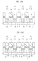
- the n - -type drift layer 2 is formed on the main surface of the n + -type SiC substrate 1. Subsequently, the n + -type source layer 3 is formed on the n - -type drift layer 2, and then the plurality of shallow trenches 4 are formed in the n - -type drift layer 2 by dry etching with the silicon oxide film 21 used as a mask.
- n-type impurities nitrogen
- n-type drift layer 2 below the shallow trenches 4, thereby forming the n-type counter dope layers 5.
- the processes so far are the same as those shown in FIG. 2A to FIG. 4A of the first embodiment.
- p-type impurities (aluminum) are ion-implanted to the n - -type drift layer 2 below the shallow trenches 4, thereby forming the p-type gate layers 35.
- This ion implantation of the p-type impurities is performed by a vertical ion implantation method, and as with the second embodiment, the ion implantation is performed with a high acceleration voltage of about 200 KeV to 600 KeV, thereby forming the p-type gate layers 35 in a deep region of the n - -type drift layer 2.
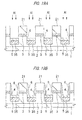
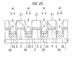
- the sidewall spacers 6 made of a silicon oxide film are formed on the sidewalls of the silicon oxide film 21 and the shallow trenches 4 by a method similar to that of the first embodiment. Then, as shown in FIG. 20 , with the silicon oxide film 21 and the sidewall spacers 6 used as masks, p-type impurities (aluminum) are ion-implanted to the n - -type drift layer 2 below the shallow trenches 4, thereby forming the p-type gate layers 35.
- p-type impurities aluminum
- This ion implantation of the p-type impurities is performed by a vertical ion implantation method, and as with the second embodiment, the ion implantation is performed with a low acceleration voltage lower than 200 KeV, thereby forming the p-type gate layers 36 in a shallow region of the n - -type drift layer 2.
- the p-type gate layer has a retrograde structure composed of the p-type gate layer 35 formed in the deep region of the n - -type drift layer 2 and having a wide width and the p-type gate layer 36 formed in the shallow region of the n - -type drift layer 2 and having a narrow width.
- the n-type counter dope layer 5 is disposed so as to be adjacent to the p-type gate layer 36 formed in the shallow region.
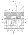
- the vertical junction FET of the first embodiment and the vertical junction FET of the second embodiment are combined together in the third embodiment, it is also possible to combine the vertical junction FET of the modification example of the first embodiment and the vertical junction FET of the second embodiment together as shown in FIG. 21 .
Landscapes
- Junction Field-Effect Transistors (AREA)
- Electrodes Of Semiconductors (AREA)
Abstract
Description
- The present invention relates to a manufacturing method of a semiconductor device and a semiconductor device, and more particularly relates to a technique effectively applied to a semiconductor device having a junction field effect transistor (JFET) formed on a silicon carbide (SiC) substrate.
- A junction field effect transistor (hereinafter, referred to as junction FET) which controls a channel with using a pn junction as a gate has been known as one of power semiconductor elements. In particular, a junction FET using SiC as a substrate material is excellent in withstand voltage characteristic because SiC has a dielectric breakdown field larger than that of Si, and since the pn junction has a high diffusion potential, a so-called normally-off FET, which can completely deplete a channel even without applying a negative voltage to a gate, can be achieved.
- Japanese Patent Application Laid-Open Publications No.
2007-128965 2011-171421 - An on-resistance which is one of important characteristics representing the performance of a junction FET can be reduced by increasing an interval between adjacent gate regions. If doing so, however, the source and drain withstand voltages at the time of a reverse bias are decreased. More specifically, the on-resistance and the source and drain withstand voltages have a tradeoff relation with the interval between gate regions as a parameter. Therefore, the control of this parameter is very important for the improvement of the performance of the junction FET.
- Mater. Sci, Forum 600-603. 1059 (2009) (Non-Patent Document 1) reports that it is possible to improve the above-described tradeoff relation between the on-resistance and the source and drain withstand voltages by making the impurity concentration profile of the p-type gate region steep. Although the
Non-Patent Document 1 does not describe how to make the impurity concentration profile steep, for example, a method in which an oblique ion implantation method is used to dope the sidewalls of the trench with n-type impurities (for example, nitrogen), thereby compensating for the impurity concentration at an end of the p-type gate region may be adopted (seeFIG. 3 of Non-Patent Document 1). - Japanese Patent Application Laid-Open Publication No.
10-294471 Patent Document 3 describes that the performance of the junction FET can be further improved by making a retrograde profile in which the width of the p-type gate region on a drain side is wider than that on a source side. Here, the width of the p-type gate region is adjusted by ion implantation energy and the dose amount of impurities. - On the other hand, Japanese Patent Application Laid-Open Publication No.
2004-134547 FIG. 5 of the Patent Document 4). -
- Patent Document 1: Japanese Patent Application Laid-Open Publication No.
2007-128965 - Patent Document 2: Japanese Patent Application Laid-Open Publication No.
2011-171421 - Patent Document 3: Japanese Patent Application Laid-Open Publication No.
10-294471 - Patent Document 4: Japanese Patent Application Laid-Open Publication No.
2004-134547 - Non-Patent Document 1: Mater. Sci, Forum 600-603. 1059 (2009)
- For the accurate control of the interval between adjacent p-type gate regions and the impurity concentration profile of the p-type gate region in the above-described conventional trench-type junction FET, there are many parameters be controlled such as the taper angle of the trench, the film thickness and shape of an oxide film used as an etching mask for the trench, and angle accuracy of an ion implantation device in addition to the process dimensions of the trench. For this reason, in consideration of mass productivity, it is difficult to ensure a process margin to obtain stable high yields.
- Also, for the improvement of the performance of the junction FET, in particular, for the reduction of the on-resistance, it is required to increase a ratio of the source area occupying the active region, and for its achievement, the reduction of the width of the gate region is necessary. In a conventional art, however, since the gate region is formed by doping the sidewalls of the trench with impurities by an oblique ion implantation method, if the width of the trench is narrowed, a ratio of the depth with respect to the width of the trench (aspect ratio) is increased, so that it becomes difficult to dope the sidewalls of the region with impurities. More specifically, it is difficult to reduce the width of the gate region in the conventional method in which the gate region is formed by doping the sidewalls of the trench with impurities by the oblique ion implantation method.
- Other problems and novel features will become apparent from the description of the specification and the attached drawings.
- One embodiment of this application is a manufacturing method of a semiconductor device having a junction field effect transistor formed on a main surface of a semiconductor substrate of a first conductivity type, and the method includes:
- (a) a step of forming a source layer of the first conductivity type on a surface of a drift layer of the first conductivity type formed on the semiconductor substrate;
- (b) after the step (a), a step of forming a plurality of trenches disposed at predetermined intervals by etching the surface of the drift layer with a first insulating film formed on the drift layer used as a mask;
- (c) after the step (b), a step of forming a counter dope layer of the first conductivity type by doping the drift layer below each of the plurality of trenches with impurities by using a vertical ion implantation method;
- (d) after the step (c), a step of forming a sidewall spacer on each sidewall of the first insulating film and the trenches; and
- (e) after the step (d), a step of forming a gate layer of a second conductivity type by doping the drift layer below each of the plurality of trenches with third impurities by using the vertical ion implantation method.
- According to the embodiment mentioned above, high-performance junction FETs can be manufactured with high yields.
-
-
FIG. 1 is a sectional view of a part of an active region of a SiC substrate having a vertical junction FET of a first embodiment formed thereon; -
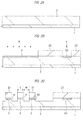
FIG. 2A is a sectional view of a principal part of the SiC substrate showing a manufacturing method of the vertical junction FET of the first embodiment; -
FIG. 2B is a sectional view of a principal part of the SiC substrate showing the manufacturing method of the vertical junction FET continued fromFIG. 2A ; -
FIG. 2C is a sectional view of a principal part of the SiC substrate showing the manufacturing method of the vertical junction FET continued fromFIG. 2B ; -
FIG. 3 is a plan view of a principal part of the SiC substrate showing the manufacturing method of the vertical junction FET of the first embodiment; -
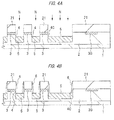
FIG. 4A is a sectional view of a principal part of the SiC substrate showing the manufacturing method of the vertical junction FET continued fromFIG. 2C ; -
FIG. 4B is a sectional view of a principal part of the SiC substrate showing the manufacturing method of the vertical junction FET continued fromFIG. 4A ; -
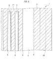
FIG. 5 is a plan view of a principal part of the SiC substrate showing the manufacturing method of the vertical junction FET continued fromFIG. 2C ; -
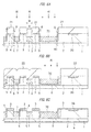
FIG. 6A is a sectional view of a principal part of the SiC substrate showing the manufacturing method of the vertical junction FET continued fromFIG. 4B ; -
FIG. 6B is a sectional view of a principal part of the SiC substrate showing the manufacturing method of the vertical junction FET continued fromFIG. 6A ; -
FIG. 6C is a sectional view of a principal part of the SiC substrate showing the manufacturing method of the vertical junction FET continued fromFIG. 6B ; -
FIG. 7A is a sectional view of a principal part of the SiC substrate showing the manufacturing method of the vertical junction FET continued fromFIG. 6C ; -
FIG. 7B is a sectional view of a principal part of the SiC substrate showing the manufacturing method of the vertical junction FET continued fromFIG. 7A ; -
FIG. 7C is a sectional view of a principal part of the SiC substrate showing the manufacturing method of the vertical junction FET continued fromFIG. 7B ; -
FIG. 8A is a sectional view of a principal part of the SiC substrate showing the manufacturing method of the vertical junction FET continued fromFIG. 7C ; -
FIG. 8B is a sectional view of a principal part of the SiC substrate showing the manufacturing method of the vertical junction FET continued fromFIG. 8A ; -
FIG. 8C is a sectional view of a principal part of the SiC substrate showing the manufacturing method of the vertical junction FET continued fromFIG. 8B ; -
FIG. 9A is a sectional view of a principal part of the SiC substrate showing the manufacturing method of the vertical junction FET continued fromFIG. 8C ; -
FIG. 9B is a sectional view of a principal part of the SiC substrate showing the manufacturing method of the vertical junction FET continued fromFIG. 9A ; -
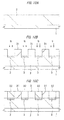
FIG. 10A is a sectional view of a principal part of a SiC substrate showing a manufacturing method of a vertical junction FET of a modification example of the first embodiment; -
FIG. 10B is a sectional view of a principal part of the SiC substrate showing the manufacturing method of the vertical junction FET continued fromFIG. 10A ; -
FIG. 10C is a sectional view of a principal part of the SiC substrate showing the manufacturing method of the vertical junction FET continued fromFIG. 10B ; -
FIG. 11A is a sectional view of a principal part of the SiC substrate showing the manufacturing method of the vertical junction FET continued fromFIG. 10C ; -
FIG. 11B is a sectional view of a principal part of the SiC substrate showing the manufacturing method of the vertical junction FET continued fromFIG. 11A ; -
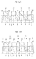
FIG. 12A is a sectional view of a principal part of the SiC substrate showing the manufacturing method of the vertical junction FET continued fromFIG. 11B ; -
FIG. 12B is a sectional view of a principal part of the SiC substrate showing the manufacturing method of the vertical junction FET continued fromFIG. 12A ; -
FIG. 13 is a sectional view of a part of an active region of the SiC substrate having the vertical junction FET of the modification example of the first embodiment formed thereon; -
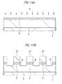
FIG. 14A is a sectional view of a principal part of a SiC substrate showing a manufacturing method of a vertical junction FET of a second embodiment; -
FIG. 14B is a sectional view of a principal part of the SiC substrate showing the manufacturing method of the vertical junction FET continued fromFIG. 14A ; -
FIG. 15A is a sectional view of a principal part of the SiC substrate showing the manufacturing method of the vertical junction FET continued fromFIG. 14B ; -
FIG. 15B is a sectional view of a principal part of the SiC substrate showing the manufacturing method of the vertical junction FET continued fromFIG. 15A ; -
FIG. 16 is a sectional view of a part of an active region of the SiC substrate having the vertical junction FET of the second embodiment formed thereon; -
FIG. 17 is a sectional view of a part of an active region of a SiC substrate having a vertical junction FET of a third embodiment formed thereon; -
FIG. 18A is a sectional view of a principal part of the SiC substrate showing a manufacturing method of the vertical junction FET of the third embodiment; -
FIG. 18B is a sectional view of a principal part of the SiC substrate showing the manufacturing method of the vertical junction FET continued fromFIG. 18A ; -
FIG. 19A is a sectional view of a principal part of the SiC substrate showing the manufacturing method of the vertical junction FET continued fromFIG. 18B ; -
FIG. 19B is a sectional view of a principal part of the SiC substrate showing the manufacturing method of the vertical junction FET continued fromFIG. 19A ; -
FIG. 20 is a sectional view of a principal part of the SiC substrate showing the manufacturing method of the vertical junction FET continued fromFIG. 19B ; and -
FIG. 21 is a sectional view of a part of an active region of a SiC substrate having a vertical junction FET of another embodiment formed thereon. - Hereinafter, embodiments of the present invention will be described in detail with reference to the accompanying drawings. Note that components having the same function are denoted by the same reference symbols throughout the drawings for describing the embodiments, and the repetitive description thereof will be omitted. In addition, in the embodiments below, the description of the same or similar portions is not repeated in principle unless particularly required. Also, in some drawings used in the following embodiments, hatching is used even in a plan view and hatching is omitted even in a sectional view so as to make the structure easily understood.
-
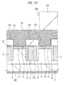
FIG. 1 is a sectional view of a part of an active region of a SiC substrate having a vertical junction FET of a first embodiment formed thereon. - On a main surface of an n+-
type SiC substrate 1 serving as a drain region of the vertical junction FET, an n--type drift layer 2 having an impurity concentration lower than that of the n+-type SiC substrate 1 is formed, and on a surface of the n--type drift layer 2, a plurality of n+-type source layers 3 having an impurity concentration higher than that of the n+-type SiC substrate 1 are formed at predetermined intervals. These n+-type source layers 3 extend in a stripe shape along a first direction (vertical direction with respect to the paper sheet) of the main surface of the n+-type SiC substrate 1. - On the surface of each of the n+-type source layers 3, a
source contact layer 11 made of a Ni (nickel) silicide film is formed. Thesource contact layer 11 is electrically connected to asource electrode 16 through acontact hole 15 formed in aninterlayer insulating film 28 which covers the n+-type source layer 3. Theinterlayer insulating film 28 is made of a silicon oxide film, and thesource electrode 16 is made of a metal film containing Al (aluminum) as a main component. - In the surface of the n--
type drift layer 2,shallow trenches 4 are formed between adjacent n+-type source layers 3 along an extending direction (first direction) of the n+-type source layers 3, and on the n--type drift layer 2 below eachshallow trench 4, a p-type gate layer 7 is formed. Also, asidewall spacer 14 made of a silicon oxide film is formed on each sidewall of theshallow trenches 4. Furthermore, in the n--type drift layer 2 below thesidewall spacer 14, an n-typecounter dope layer 5 is formed so as to be adjacent to the p-type gate layer 7. - One of the features of the vertical junction FET of the first embodiment is that, as shown in
FIG. 1 , the bottom surface of theshallow trench 4 is positioned lower than the n+-type source layer 3 and thesidewall spacer 14 made of an insulating material (silicon oxide) is formed on the sidewall of theshallow trench 4, so that the n+-type source layer 3 and the p-type gate layer 7 are not in contact with each other. - Another feature of the vertical junction FET of the first embodiment is that, as will be described further below, the n--
type drift layer 2 below theshallow trench 4 is doped with impurities by using the vertical ion implantation method, thereby forming the n-typecounter dope layer 5 and the p-type gate layer 7. - On the surface of the p-
type gate layer 7 formed on the n--type drift layer 2 below theshallow trench 4, agate contact layer 12 made of a Ni silicide film is formed. Thegate contact layer 12 is electrically connected to a gate electrode (gate electrode 17 described further below) made of a metal film of the same layer as thesource electrode 16 via a contact hole formed in theinterlayer insulating film 28 at an end of the active region (not shown). - On the uppermost portion of the main surface of the n+-
type SiC substrate 1, asurface protection film 19 made of a polyimide resin film is formed. As shown inFIG. 1 , anopening 29 is formed in thesurface protection film 19, and thesource electrode 16 exposed on the bottom of theopening 29 forms a source pad. Although not shown, another opening is formed in thesurface protection film 19, and thegate electrode 17 exposed on the bottom of this opening forms a gate pad. - Although
FIG. 1 shows only a part of the active region of the n+-type SiC substrate 1, a termination layer (p--type termination layer 8 described further below) for mitigating the electric field of the active region is formed on the circumference of the active region not shown in the drawing. The p--type termination layer 8 is a p-type semiconductor region formed by ion-implanting impurities to the n--type drift layer 2 on the circumference of the active region. Also, a guard ring (n+-typeguard ring layer 3G andguard ring wiring 18 described further below) is formed on a further outer side of the termination layer, that is, on the outer circumference of the n+-type SiC substrate 1. The n+-typeguard ring layer 3G is an n-type semiconductor region formed by ion-implanting impurities to the n--type drift layer 2 on the outer circumference of the n+-type SiC substrate 1, and theguard ring wiring 18 is made of a metal film of the same layer as thesource gate 16 and thegate electrode 17. - On the other hand, a
drain electrode 30 is formed on the back surface of the n+-type SiC substrate 1. Thedrain electrode 30 is made of a conductive film containing Ni (nickel) silicide as a main component. As described above, the vertical junction FET of the first embodiment has a three-terminal structure having the source pad and the gate pad provided on the main surface side of the n+-type SiC substrate 1 and thedrain electrode 30 provided on the back surface side of the n+-type SiC substrate 1. - The operation of the vertical junction FET of the first embodiment is basically the same as the operation of a conventional vertical junction FET, and on/off of the current flowing between the source and the drain is switched by controlling the width of a depletion layer extending from the p-
type gate layer 7 to the channel (n--type drift layer 2 below n+-type source layer 3). More specifically, in an OFF state, a negate voltage is applied to the gate (p-type gate layer 7) to expand the depletion layer from the gate to the channel, thereby preventing carriers (electrons) from flowing between the source and the drain. On the other hand, in an ON state, a positive voltage is applied to the gate and the drain to reduce the depletion layer, thereby causing carries (electrons) to flow from the source to the drain. - Next, a manufacturing method of the vertical junction FET of the first embodiment is described with reference to the drawings in the order of the process. Here, a vertical junction FET having a withstand voltage equal to or higher than 600 V is assumed.
- First, as shown in
FIG. 2A , on the main surface of the n+-type SiC substrate 1 doped with n-type impurities (nitrogen) at a high concentration, the n--type drift layer 2 is formed by using an epitaxial growth method. The n--type drift layer 2 has an impurity (nitrogen) concentration of about 2×10¹⁶ atom/cm3 and a thickness of about 6 µm. - Next, as shown in
FIG. 2B , a silicon oxide film (first insulating film) 20 is deposited on the main surface of the n+-type SiC substrate 1 by using CVD, and then thesilicon oxide film 20 is patterned by dry etching with a photoresist film (not shown) used as a mask. Subsequently, with thissilicon oxide film 20 used as a mask, n-type impurities (nitrogen) are ion-implanted to the n--type drift layer 2, thereby forming the n+-type source layer 3. At this time, the n-type impurities are ion-implanted also to the n--type drift layer 2 on the outer circumference of the n+-type SiC substrate 1, thereby forming the n+-typeguard ring layer 3G surrounding the active region. The n+-type source layer 3 and the n+-typeguard ring layer 3G have an impurity concentration of about 1×10²⁰ atom/cm3. - Next, after the
silicon oxide film 20 is removed, as shown inFIG. 2C , asilicon oxide film 21 is deposited on the main surface of the n+-type SiC substrate 1 by using CVD, and thesilicon oxide film 21 is patterned by dry etching with a photoresist film used as a mask. Subsequently, with thissilicon oxide film 21 used as a mask, the n+-type source layer 3 and the n--type drift layer 2 therebelow are subjected to dry etching, thereby forming a plurality ofshallow trenches 4. At this time, the n--type drift layer 2 at an end of the active region is also subj ect to dry etching, thereby forming ashallow trench 4C having a width wider than that of theshallow trenches 4. - As shown in
FIG. 2C , theshallow trenches type drift layer 2 to the bottom surface of theshallow trenches shallow trenches 4 in the n--type drift layer 2 of the active region, the n+-type source layers 3 are separated via theshallow trenches 4. The width (S) of each of the n+-type source layers 3, in other words, an interval between adjacentshallow trenches 4 is about 1.0 µm. Also, eachshallow trench 4 has a width (W) of about 1.0 µm. - As shown in
FIG. 3 , theshallow trenches 4 formed in the n--type drift layer 2 of the active region extend in a stripe shape along one direction of the main surface of the n+-type SiC substrate 1. - An object of forming the
shallow trenches type drift layer 2 is to dope a deep region of the n--type drift layer 2 with impurities (impurities for forming the n-typecounter dope layer 5 and impurities for forming the p-type gate layer 7) in the next ion implantation process. Therefore, when an energy ion implantation device with high acceleration voltage is used to dope the region with impurities, the depth of theshallow trenches type source layer 3. - Next, as shown in
FIG. 4A , with thesilicon oxide film 21 used as a mask, n-type impurities (nitrogen) are ion-implanted to the n--type drift layer 2 below theshallow trenches counter dope layer 5 has the impurity (nitrogen) concentration of about 1×10¹⁷ atom/cm3. Also, the ion implantation of the n-type impurities is performed by multi-step implantation with varied acceleration voltages, and the depth of the n-typecounter dope layer 5 is about 0.8 µm to 1 µm from the surface of the n--type drift layer 2. - The n-type
counter dope layer 5 is formed so as to compensate for diffusion of impurities (aluminum) of the p-type gate layer 7 to be formed in the next process in a lateral direction (channel direction) and make the impurity concentration profile of the p-type gate layer 7 steep. - Next, as shown in
FIG. 4B andFIG. 5 , thesidewall spacer 6 is formed on each of the sidewalls of thesilicon oxide film 21 and theshallow trenches sidewall spacer 6 is formed by depositing a silicon oxide film on the main surface of the n+-type SiC substrate 1 by using CVD and then performing anisotropic etching to this silicon oxide film. - Next, as shown in
FIG. 6A , with thesilicon oxide film 21 and thesidewall spacers 6 used as masks, p-type impurities (aluminum or boron) are ion-implanted to the n--type drift layer 2 below theshallow trenches 4, thereby forming the p-type gate layers 7 in a self-alignment manner with respect to thesidewall spacers 6. At this time, p-type impurities are ion-implanted also to the n--type drift layer 2 at the end of the active region, thereby forming a p-type gate layer 7C having a width wider than that of the p-type gate layer 7. - Ion implantation of the p-type impurities is performed by a vertical ion implantation method, and the impurity concentration of the p-type gate layers 7 and 7C is about 1×10¹⁸ atom/cm3. Also, ion implantation of the p-type impurities is performed by multi-step implantation with varied acceleration voltages, and the depth of the p-type gate layers 7 and 7C is approximately equal to the depth of the n-type counter dope layer 5 (about 0.8 µm to 1 µm from the surface of the n--type drift layer 2).
- As described above, in the first embodiment, after the
sidewall spacers 6 are formed on the sidewalls of theshallow trenches 4, the n--type drift layer 2 below theshallow trenches 4 is doped with p-type impurities by using the vertical ion implantation method, thereby forming the p-type gate layers 7 in a self-alignment manner with respect to thesidewall spacers 6. - In this manner, the width (G) of the p-
type gate layer 7 can be made narrower than the width (W) of theshallow trench 4. More specifically, when the width (W) of theshallow trench 4 is made narrow to a processing limit, the width (G) of the p-type gate layer 7 can be further made narrower than this processing limit. Also, since the width of thesidewall spacers 6 to be formed on the sidewalls of theshallow trenches 4 can be accurately controlled by defining the film thickness of the silicon oxide film which is a material of thesidewall spacers 6, the width (G) of the p-type gate layer 7 can also be accurately controlled. Furthermore, since the p-type gate layers 7 are formed in the state where thesidewall spacers 6 are formed on the sidewalls of theshallow trenches 4, the n+-type source layers 3 and the p-type gate layers 7 are prevented from being in contact with each other. In particular, in the first embodiment, since theshallow trenches 4 are formed deeper than the n+-type source layers 3, the n+-type source layers 3 and the p-type gate layers 7 are further reliably prevented from being in contact with each other. - Next, after the
silicon oxide film 21 and thesidewall spacers 6 are removed, as shown inFIG. 6B , asilicon oxide film 22 is deposited on the main surface of the n+-type SiC substrate 1 by using CVD, and thesilicon oxide film 22 is patterned by dry etching with a photoresist film used as a mask. Subsequently, with thissilicon oxide film 22 used as a mask, p-type impurities (aluminum or boron) are ion-implanted to the n--type drift layer 2 on the circumference of the active region, thereby forming the p--type termination layer 8. The p--type termination layer 8 is a semiconductor region for the purpose of mitigating the electric field of the active region, and is formed in a region deeper than the p-type gate layer 7C. Also, the impurity concentration of the p--type termination layer 8 is about 1×10¹⁷ atom/cm3. - Next, after the
silicon oxide film 21 and thesidewall spacers 6 are removed, the n+-type SiC substrate 1 is annealed, thereby activating the n-type impurities (nitrogen) and the p-type impurities (aluminum or boron) with which the n--type drift layer 2 has been doped in the above-described process. Here, the anneal temperature of the n+-type SiC substrate 1 is about 1700°C to 1800°C. When the n+-type SiC substrate 1 is annealed, the main surface side and the back surface side of the n+-type SiC substrate 1 are coated with acarbon layer 9 as shown inFIG. 6C in order to prevent vaporization of Si constituting the n+-type SiC substrate 1. - Next, after the
carbon layer 9 is removed, as shown inFIG. 7A , asilicon oxide film 23 is deposited on the main surface of the n+-type SiC substrate 1 by using CVD. Subsequently, abarrier metal film 24 made of a TiN (titanium nitride) film is deposited on thesilicon oxide film 23 by using sputtering. - Next, as shown in
FIG. 7B , thebarrier metal film 24 and thesilicon oxide film 23 of the active region are subjected to anisotropic etching, thereby formingsidewall spacers 10 made of a laminated film of thebarrier metal film 24 and thesilicon oxide film 23 on the sidewalls of theshallow trenches 4. At this time, the outside of the active region is covered with aphotoresist film 26 having anopening 25 provided above the n+-typeguard ring layer 3G, and thebarrier metal film 24 and thesilicon oxide film 23 on the bottom of theopening 25 are etched, thereby exposing the surface of the n+-typeguard ring layer 3G. - Next, after the
photoresist film 26 is removed, as shown inFIG. 7C , aNi film 27 is deposited on the main surface of the n+-type SiC substrate 1 by sputtering. Subsequently, the n+-type SiC substrate 1 is annealed, thereby causing each of the n+-type source layers 3 and the p-type gate layers 7 and 7C to react with the Ni film 27 (silicidation reaction). - Next, the
unreacted Ni film 27 and thebarrier metal film 24 are removed. In this manner, as shown inFIG. 8A , thesource contact layer 11 made of a Ni silicide film is formed on each surface of the n+-type source layer 3, and thegate contact layer 12 made of a Ni silicide film is formed on each surface of the p-type gate layers 7 and 7C. Also, a guardring contact layer 13 made of a Ni silicide film is formed on the surface of the n+-typeguard ring layer 3G. - The
source contact layer 11 is a conducive layer for the ohmic connection between the n+-type source layer 3 and thesource electrode 16 to be formed in a later process, and thegate contact layer 12 is a conductive layer for the ohmic connection between the p-type gate layers 7 and 7C and the gate electrode to be formed in a later process. Also, the guardring contact layer 13 is a conductive layer for the ohmic connection between the n+-typeguard ring layer 3G and theguard ring wiring 18 to be formed in a later process. - Also, by removing the
barrier metal films 24 constituting parts of thesidewall spacers 10, thesidewall spacers 14 made of thesilicon oxide film 23 are formed on the sidewalls of theshallow trenches - Next, as shown in
FIG. 8B , after theinterlayer insulating film 28 made of a silicon oxide film is deposited on the main surface of the n+-type SiC substrate 1 by using CVD, theinterlayer insulating film 28 is patterned by dry etching with a photoresist film used as a mask, thereby forming acontact hole 15 on each of the n+-type source layers 3, the p-type gate layer 7C, and the n+-typeguard ring layer 3G. Also, in a region not shown in the drawings, a contact hole is formed also in thesilicon oxide film 28 on the p-type gate layer 7. - Next, as shown in
FIG. 8C , after a metal film containing Al as a main component is deposited on the main surface of the n+-type SiC substrate 1 by sputtering, this metal film is patterned by dry etching with a photoresist film used as a mask. In this manner, thesource electrode 16 electrically connected to thesource contact layer 11 on the surface of the n+-type source layer 3, thegate electrode 17 electrically connected to thegate contact layer 12 of the p-type gate layer 7C, and theguard ring wiring 18 electrically connected to the guardring contact layer 13 on the surface of the n+-typeguard ring layer 3G are formed. In a region not shown in the drawings, thegate electrode 17 is electrically connected also to thegate contact layer 12 on the surface of the p-type gate layer 7. - Next, as shown in
FIG. 9A , after thesurface protection film 19 made of a polyimide resin film is formed on the uppermost part of the main surface of the n+-type SiC substrate 1, theopening 29 is formed in thesurface protection film 19 on thesource electrode 16. The source electrode 16 exposed to the bottom of thisopening 29 forms a source pad. Also, in a region not shown in the drawings, an opening is formed in thesurface protection film 19 on thegate electrode 17, thereby forming a gate pad. - Next, as shown in
FIG. 9B , thedrain electrode 30 is formed on the entire back surface of the n+-type SiC substrate 1, thereby completing the vertical junction FET of the first embodiment shown inFIG. 1 . Thedrain electrode 30 is made of a Ni silicide film and has a surface plated with Au (gold). - In the vertical junction FET of the first embodiment fabricated through the process described above, the following effects can be obtained.
- Since the n-type
counter dope layer 5 and the p-type gate layer 7 are formed in the n--type drift layer 2 by using the vertical ion implantation method, the impurity concentration profile of the p-type gate layer 7 can be accurately controlled in comparison with a conventional manufacturing method of a trench-type junction FET, in which the sidewalls and bottom surface of a trench are doped with p-type impurities by using an oblique ion implantation method and a vertical ion implantation method in combination, thereby forming a p-type gate region. - Also, since it becomes unnecessary to consider diffusion variations of the impurities in a lateral direction caused due to the oblique ion implantation method, the dimensional accuracy of the width (G) of the p-
type gate layer 7 can be improved. This means that a process margin for obtaining stable high yields can be easily ensured and a more severe on-resistance design can be made while ensuring a withstand voltage margin. - Furthermore, since the p-
type gate layer 7 is formed in a self-alignment manner with respect to thesidewall spacers 6 formed on the sidewalls of theshallow trenches 4, the width (G) of the p-type gate layer 7 can be made narrower than the processing limit. Therefore, since a ratio of an area of the n+-type source layer 3 serving as a current path occupying the active region can be increased, the density of the current flowing between the source and the drain can be improved and the on-resistance of the whole chip can be reduced. In other words, the chip size can be reduced without reducing the current density. - In the structure in which the n+-
type source layer 3 and the p-type gate layer 7 are in contact with each other, the occurrence of a leakage current at a junction part therebetween is a matter of concern (see Patent Document 2). However, since the n+-type source layer 3 and the p-type gate layer 7 are not in contact with each other, the leakage current can be suppressed. - In the first embodiment, after the
shallow trenches 4 are formed in the n--type drift layer 2, impurities are ion-implanted to the n--type drift layer 2 below theshallow trenches 4, thereby forming the n-type counter dope layers 5 and the p-type gate layer 7C. Alternatively, the n-type counter dope layers 5 and the p-type gate layer 7C can be formed while omitting theshallow trenches 4 by the following method. - First, after the n--
type drift layer 2 is formed on the main surface of the n+-type SiC substrate 1 by a method similar to that of the first embodiment as shown inFIG. 10A , asilicon oxide film 31 is deposited on the main surface of the n+-type SiC substrate 1 by using CVD, and thesilicon oxide film 31 is patterned by dry etching with a photoresist film used as a mask as shown inFIG. 10B . Subsequently, with thissilicon oxide film 31 used as a mask, n-type impurities (nitrogen) are ion-implanted to the n--type drift layer 2, thereby forming the n+-type source layers 3. - Next, as shown in
FIG. 10C , after asilicon nitride film 32 is deposited on the main surface of the n+-type SiC substrate 1 by using CVD, thesilicon nitride film 32 is polished by using chemical-mechanical polishing so as to recede until the surface of thesilicon nitride film 32 is exposed. - Next, as shown in
FIG. 11A , thesilicon oxide film 31 is selectively etched by using a difference in etching rate between thesilicon oxide film 31 and thesilicon nitride film 32, thereby leaving thesilicon nitride film 32 on each of the n+-type source layers 3. - Next, as shown in
FIG. 11B , n-type impurities (nitrogen) are ion-implanted to the n--type drift layer 2 with thesilicon nitride film 32 used as a mask, thereby forming the n-type counter dope layers 5. As with the first embodiment, the n-type counter dope layers 5 are formed by using a vertical ion implantation method performed by multi-step implantation of n-type impurities with varied acceleration voltages. - Next, as shown in
FIG. 12A , after a silicon nitride film is deposited on the main surface of the n+-type SiC substrate 1 by using CVD, this silicon nitride film is subjected to anisotropic etching, thereby formingsidewall spacers 33 on sidewalls of thesilicon nitride films 32. - Next, as shown in
FIG. 12B , with thesilicon nitride films 32 and thesidewall spacers 33 used as masks, p-type impurities (aluminum or boron) are ion-implanted to the n--type drift layer 2, thereby forming the p-type gate layers 7 in a self-alignment manner with respect to thesidewall spacers 33. The p-type gate layers 7 are formed by using a vertical ion implantation method performed by multi-step implantation of p-type impurities with varied acceleration voltages. - The processes thereafter are approximately similar to those of the first embodiment, and therefore are not described here.
FIG. 13 is a sectional view of a part of an active region of the SiC substrate having the vertical junction FET of the modification example of the first embodiment formed thereon. - Also in this modification example, since the n-type counter dope layers 5 and the p-type gate layers 7 are formed by doping of impurities by using the vertical ion implantation method, the dimensional accuracy of the width (G) of the p-
type gate layer 7 can be improved in comparison with the conventional manufacturing method of a trench-type junction FET. - Also, since the ratio of an area of the n+-
type source layer 3 occupying the active region can be increased, the density of the current flowing between the source and the drain can be improved and the on-resistance of the whole chip can be decreased. - Furthermore, since the n+-
type source layer 3 and the p-type gate layer 7 are not in contact with each other via the n-typecounter dope layer 5, a leakage current can also be suppressed. - A manufacturing method of a vertical junction FET of a second embodiment is described with reference to the drawings in the order of the process.
- First, as shown in
FIG. 14A , after the n--type drift layer 2 is formed on the main surface of the n+-type SiC substrate 1, n-type impurities (nitrogen) are ion-implanted to the n--type drift layer 2 of the active region, thereby forming the n+-type source layer 3. Subsequently, as shown inFIG. 14B , after thesilicon oxide film 21 deposited on the main surface of the n+-type SiC substrate 1 is patterned, the n+-type source layer 3 and the n--type drift layer 2 therebelow are subjected to dry etching with thissilicon oxide film 21 used as a mask, thereby forming the plurality ofshallow trenches 4. The processes so far are similar to those shown inFIG. 2A to FIG. 2C of the first embodiment. - Next, as shown in
FIG. 15A , with thesilicon oxide film 21 used as a mask, p-type impurities (aluminum or boron) are ion-implanted to the n--type drift layer 2 below theshallow trenches 4, thereby forming p-type gate layers (first gate layer) 35. At this time, as with the p-type gate layers 7 of the first embodiment, ion implantation of p-type impurities is performed by a vertical ion implantation method, but the ion implantation is performed with a high acceleration voltage of about 200 KeV to 600 KeV in this case, thereby forming the p-type gate layers 35 in a deep region of the n--type drift layer 2. - Next, as shown in
FIG. 15B , thesidewall spacers 6 made of a silicon oxide film are formed on the sidewalls of thesilicon oxide film 21 and theshallow trenches 4 by a method similar to that of the first embodiment. Then, with thesilicon oxide film 21 and thesidewall spacers 6 used as masks, p-type impurities (aluminum or boron) are ion-implanted to the n--type drift layer 2 below theshallow trenches 4, thereby forming p-type gate layers 36 (second gate layer). At this time, as with the p-type gate layers 7 of the first embodiment, ion implantation of p-type impurities is performed by a vertical ion implantation method, but the ion implantation is performed with a low acceleration voltage lower than 200 KeV in this case, thereby forming the p-type gate layers 36 in a shallow region of the n--type drift layer 2, that is, on the p-type gate layers 35. Also, the impurity concentration of the p-type gate layer 36 is approximately the same as the impurity concentration of the p-type gate layer 35. - In this manner, the p-type gate layer has a retrograde structure composed of the p-
type gate layer 35 formed in the deep region of the n--type drift layer 2 and having a wide width and the p-type gate layer 36 formed in the shallow region of the n--type drift layer 2 and having a narrow width. - The processes thereafter are approximately similar to those of the first embodiment, and therefore are not described here.
FIG. 16 is a sectional view of a part of an active region of the SiC substrate having the vertical junction FET of the second embodiment formed thereon. - According to the second embodiment, since the p-type gate layers 35 and 36 are formed by doping of impurities by using the vertical ion implantation method, the dimensional accuracy of the widths of the p-type gate layers 35 and 36 can be improved.
- Also, since the p-type gate layer has the retrograde structure as described above, the performance of the vertical junction FET can be enhanced.
- Furthermore, since the n+-
type source layer 3 and the p-type gate layers 35 and 36 are not in contact with each other, a leakage current can be suppressed. - A vertical junction FET of a third embodiment is obtained by combining the vertical junction FET of the first embodiment and the vertical junction FET of the second embodiment together. More specifically, as shown in
FIG. 17 , in the vertical junction FET of the third embodiment, the p-type gate layer having the retrograde structure as that of the second embodiment is adopted in the vertical junction FET of the first embodiment. - A manufacturing method of the vertical junction FET of the third embodiment is described with reference to the drawings in the order of the process.
- First, as shown in
FIG. 18A , the n--type drift layer 2 is formed on the main surface of the n+-type SiC substrate 1. Subsequently, the n+-type source layer 3 is formed on the n--type drift layer 2, and then the plurality ofshallow trenches 4 are formed in the n--type drift layer 2 by dry etching with thesilicon oxide film 21 used as a mask. - Next, as shown in
FIG. 18B , with thesilicon oxide film 21 used as a mask, n-type impurities (nitrogen) are ion-implanted to the n--type drift layer 2 below theshallow trenches 4, thereby forming the n-type counter dope layers 5. The processes so far are the same as those shown inFIG. 2A to FIG. 4A of the first embodiment. - Next, as shown in
FIG. 19A , with thesilicon oxide film 21 used as a mask, p-type impurities (aluminum) are ion-implanted to the n--type drift layer 2 below theshallow trenches 4, thereby forming the p-type gate layers 35. This ion implantation of the p-type impurities is performed by a vertical ion implantation method, and as with the second embodiment, the ion implantation is performed with a high acceleration voltage of about 200 KeV to 600 KeV, thereby forming the p-type gate layers 35 in a deep region of the n--type drift layer 2. - Next, as shown in
FIG. 19B , thesidewall spacers 6 made of a silicon oxide film are formed on the sidewalls of thesilicon oxide film 21 and theshallow trenches 4 by a method similar to that of the first embodiment. Then, as shown inFIG. 20 , with thesilicon oxide film 21 and thesidewall spacers 6 used as masks, p-type impurities (aluminum) are ion-implanted to the n--type drift layer 2 below theshallow trenches 4, thereby forming the p-type gate layers 35. This ion implantation of the p-type impurities is performed by a vertical ion implantation method, and as with the second embodiment, the ion implantation is performed with a low acceleration voltage lower than 200 KeV, thereby forming the p-type gate layers 36 in a shallow region of the n--type drift layer 2. - In this manner, the p-type gate layer has a retrograde structure composed of the p-
type gate layer 35 formed in the deep region of the n--type drift layer 2 and having a wide width and the p-type gate layer 36 formed in the shallow region of the n--type drift layer 2 and having a narrow width. Also, the n-typecounter dope layer 5 is disposed so as to be adjacent to the p-type gate layer 36 formed in the shallow region. - According to the third embodiment, the effects of the first embodiment and the effects of the second embodiment described above can be obtained.
- In the foregoing, the invention made by the inventors of the present invention has been concretely described based on the embodiments. However, it is needless to say that the present invention is not limited to the foregoing embodiments and various modifications and alterations can be made within the scope of the present invention.
- For example, although the vertical junction FET of the first embodiment and the vertical junction FET of the second embodiment are combined together in the third embodiment, it is also possible to combine the vertical junction FET of the modification example of the first embodiment and the vertical junction FET of the second embodiment together as shown in
FIG. 21 . - In addition, some of contents described in the embodiments are described below.
- (1) A manufacturing method of a semiconductor device having a junction field effect transistor formed on a main surface of a semiconductor substrate of a first conductivity type includes:
- (a) a step of forming a drift layer of the first conductivity type on the semiconductor substrate of the first conductivity type;
- (b) a step of forming a plurality of source layers of the first conductivity type disposed at predetermined intervals on a surface of the drift layer by doping the drift layer with first impurities with a first insulating film formed on the drift layer used as a mask;
- (c) after the step (b), a step of removing the first insulating film and forming a second insulating film on each of the plurality of source layers;
- (d) a step of forming a counter dope layer of the first conductivity type in the drift layer by doping the drift layer with second impurities by a vertical ion implantation method with the second insulating film used as a mask;
- (e) after the step (d), a step of forming sidewall spacers made of a third insulating film on sidewalls of the second insulating film; and
- (f) a step of forming a gate layer of a second conductivity type in the drift layer by doping the drift layer with third impurities by the vertical ion implantation method with the second insulating film and the sidewall spacers used as masks.
- (2) In the manufacturing method of a semiconductor device described in (1), the counter dope layer has an impurity concentration lower than an impurity concentration of the source layer.
- (3) In the manufacturing method of a semiconductor device described in (1), the counter dope layer is formed so as to be in contact with a side surface of the gate layer.
- (4) In the manufacturing method of a semiconductor device described in (1), the semiconductor substrate is made of silicon carbide, the first and second impurities are nitrogen, and the third impurities are aluminum or boron.
Claims (15)
- A manufacturing method of a semiconductor device having a junction field effect transistor formed on a main surface of a semiconductor substrate of a first conductivity type, comprising:(a) a step of forming a drift layer of the first conductivity type on the semiconductor substrate;(b) a step of forming a source layer of the first conductivity type on a surface of the drift layer by doping the drift layer with first impurities;(c) after the step (b), a step of forming a plurality of trenches disposed at predetermined intervals in the surface of the drift layer by etching the surface of the drift layer with a first insulating film formed on the drift layer used as a mask;(d) after the step (c), a step of forming a counter dope layer of the first conductivity type in the drift layer below each of the plurality of trenches by doping the drift layer below each of the plurality of trenches with second impurities by using a vertical ion implantation method;(e) after the step (d), a step of forming a sidewall spacer made of a second insulating film on each sidewall of the first insulating film and the trenches; and(f) after the step (e), a step of forming a gate layer of a second conductivity type in the drift layer below each of the plurality of trenches by doping the drift layer below each of the plurality of trenches with third impurities by using the vertical ion implantation method.
- The manufacturing method of a semiconductor device according to claim 1,
wherein the trenches are formed so as to each have a bottom surface positioned lower than the source layer. - The manufacturing method of a semiconductor device according to claim 1,
wherein the counter dope layer has an impurity concentration lower than an impurity concentration of the source layer. - The manufacturing method of a semiconductor device according to claim 1,
wherein the counter dope layer is formed so as to be in contact with a side surface of the gate layer. - The manufacturing method of a semiconductor device according to claim 1,
wherein the semiconductor substrate is made of silicon carbide, the first and second impurities are nitrogen, and the third impurities are aluminum or boron. - A manufacturing method of a semiconductor device having a junction field effect transistor formed on a main surface of a semiconductor substrate of a first conductivity type, comprising:(a) a step of forming a drift layer of the first conductivity type on the semiconductor substrate;(b) a step of forming a source layer of the first conductivity type on a surface of the drift layer by doping the drift layer with first impurities;(c) after the step (b), a step of forming a plurality of trenches disposed at predetermined intervals in the surface of the drift layer by etching the surface of the drift layer with a first insulating film formed on the drift layer used as a mask;(d) after the step (c), a step of forming a first gate layer of a second conductivity type in the drift layer in a region deeper than a bottom surface of each of the plurality of trenches by doping the drift layer below each of the plurality of trenches with second impurities by using a vertical ion implantation method;(e) after the step (d), a step of forming a sidewall spacer made of a second insulating film on each sidewall of the first insulating film and the trenches; and(f) after the step (e), a step of forming a second gate layer of a second conductivity type on the first gate layer in the drift layer by doping the drift layer below each of the plurality of trenches with third impurities by using the vertical ion implantation method.
- The manufacturing method of a semiconductor device according to claim 6, further comprising:after the step (c) and before the step (d), a step of forming a counter dope layer of the first conductivity type in the drift layer below each of the plurality of trenches by doping the drift layer below each of the plurality of trenches with fourth impurities by using the vertical ion implantation method.
- The manufacturing method of a semiconductor device according to claim 6,
wherein the trenches are formed so as to each have a bottom surface positioned lower than the source layer. - The manufacturing method of a semiconductor device according to claim 6,
wherein the semiconductor substrate is made of silicon carbide, the first impurities are nitrogen, and the second and third impurities are aluminum or boron. - The manufacturing method of a semiconductor device according to claim 7,
wherein the fourth impurities are nitrogen. - A semiconductor device having a junction field effect transistor formed on a main surface of a semiconductor substrate of a first conductivity type, the device comprising:a drift layer of the first conductivity type formed on the semiconductor substrate;a plurality of source layers of the first conductivity type formed at predetermined intervals on a surface of the drift layer;a plurality of trenches formed in regions between the source layers adjacent to each other in the surface of the drift layer;sidewall spacers made of an insulating film formed on each sidewall of the plurality of trenches;a gate layer of a second conductivity type formed in the drift layer below each of the plurality of trenches; anda counter dope layer of the first conductivity type formed so as to be in contact with a side surface of the gate layer in the drift layer below each of the sidewall spacers.
- The semiconductor device according to claim 11,
wherein the gate layer is composed of a first gate layer and a second gate layer formed on the first gate layer and having a width narrower than a width of the first gate layer, and
the counter dope layer is formed so as to be in contact with a side surface of the second gate layer. - The semiconductor device according to claim 11,
wherein each of the trenches has a bottom surface positioned lower than the source layer. - The semiconductor device according to claim 11,
wherein the counter dope layer has an impurity concentration lower than an impurity concentration of the source layer. - The semiconductor device according to claim 11,
wherein the semiconductor substrate is made of silicon carbide.
Applications Claiming Priority (1)
| Application Number | Priority Date | Filing Date | Title |
|---|---|---|---|
| JP2013057949A JP6073719B2 (en) | 2013-03-21 | 2013-03-21 | Semiconductor device manufacturing method and semiconductor device |
Publications (3)
| Publication Number | Publication Date |
|---|---|
| EP2782122A2 true EP2782122A2 (en) | 2014-09-24 |
| EP2782122A3 EP2782122A3 (en) | 2014-12-24 |
| EP2782122B1 EP2782122B1 (en) | 2019-02-27 |
Family
ID=50389236
Family Applications (1)
| Application Number | Title | Priority Date | Filing Date |
|---|---|---|---|
| EP14160755.6A Active EP2782122B1 (en) | 2013-03-21 | 2014-03-19 | Manufacturing method of JFET semiconductor device and JFET semiconductor device |
Country Status (4)
| Country | Link |
|---|---|
| US (2) | US9048264B2 (en) |
| EP (1) | EP2782122B1 (en) |
| JP (1) | JP6073719B2 (en) |
| CN (1) | CN104064604B (en) |
Families Citing this family (12)
| Publication number | Priority date | Publication date | Assignee | Title |
|---|---|---|---|---|
| JP6509621B2 (en) * | 2015-04-22 | 2019-05-08 | ルネサスエレクトロニクス株式会社 | Semiconductor device |
| US20170018657A1 (en) * | 2015-07-14 | 2017-01-19 | United Silicon Carbide, Inc. | Vertical jfet made using a reduced mask set |
| US10050154B2 (en) | 2015-07-14 | 2018-08-14 | United Silicon Carbide, Inc. | Trench vertical JFET with ladder termination |
| WO2018132458A1 (en) * | 2017-01-13 | 2018-07-19 | United Silicon Carbide, Inc. | Trench vertical jfet with ladder termination |
| JP2019140159A (en) * | 2018-02-06 | 2019-08-22 | 富士電機株式会社 | Semiconductor device and method of manufacturing semiconductor device |
| JP6973422B2 (en) * | 2019-01-21 | 2021-11-24 | 株式会社デンソー | Manufacturing method of semiconductor device |
| US11264496B2 (en) * | 2020-04-20 | 2022-03-01 | Polar Semiconductor, Llc | Transistor with buried p-field termination region |
| US11329147B2 (en) | 2020-05-12 | 2022-05-10 | Polar Semiconductor, Llc | Insulated gate bipolar transistor with epitaxial layer formed on recombination region |
| US12015079B2 (en) | 2021-08-30 | 2024-06-18 | Polar Semiconductor, Llc | Transistor with single termination trench having depth more than 10 microns |
| CN114068534B (en) * | 2021-11-15 | 2024-11-29 | 武汉新芯集成电路股份有限公司 | Semiconductor device and method for manufacturing the same |
| US20250040166A1 (en) * | 2023-07-25 | 2025-01-30 | Semiconductor Components Industries, Llc | Planar JFET Device with Reduced Gate Resistance |
| US20250183035A1 (en) * | 2023-12-05 | 2025-06-05 | Semiconductor Components Industries, Llc | Methods for manufacturing power semiconductor devices and power semicondudctor structures |
Citations (4)
| Publication number | Priority date | Publication date | Assignee | Title |
|---|---|---|---|---|
| JPH10294471A (en) | 1997-04-17 | 1998-11-04 | Hitachi Ltd | Silicon carbide semiconductor device and method of manufacturing the same |
| JP2004134547A (en) | 2002-10-10 | 2004-04-30 | Hitachi Ltd | Semiconductor device |
| JP2007128965A (en) | 2005-11-01 | 2007-05-24 | Renesas Technology Corp | Switching semiconductor device and manufacturing method thereof |
| JP2011171421A (en) | 2010-02-17 | 2011-09-01 | Renesas Electronics Corp | Semiconductor device and method for manufacturing the same |
Family Cites Families (14)
| Publication number | Priority date | Publication date | Assignee | Title |
|---|---|---|---|---|
| GB9922764D0 (en) * | 1999-09-28 | 1999-11-24 | Koninkl Philips Electronics Nv | Manufacture of trench-gate semiconductor devices |
| JP4564362B2 (en) * | 2004-01-23 | 2010-10-20 | 株式会社東芝 | Semiconductor device |
| US7834376B2 (en) * | 2005-03-04 | 2010-11-16 | Siliconix Technology C. V. | Power semiconductor switch |
| JP4996828B2 (en) * | 2005-03-23 | 2012-08-08 | 本田技研工業株式会社 | Method for manufacturing junction type semiconductor device |
| JP4777676B2 (en) * | 2005-03-23 | 2011-09-21 | 本田技研工業株式会社 | Junction type semiconductor device and method of manufacturing junction type semiconductor device |
| US7719055B1 (en) * | 2007-05-10 | 2010-05-18 | Northrop Grumman Systems Corporation | Cascode power switch topologies |
| US7825487B2 (en) * | 2008-09-30 | 2010-11-02 | Northrop Grumman Systems Corporation | Guard ring structures and method of fabricating thereof |
| EP2345082A4 (en) * | 2008-11-05 | 2013-07-31 | Ss Sc Ip Llc | VERTICAL JUNCTION FIELD EFFECT TRANSISTORS COMPRISING SLIDING SIDEWALLS AND METHODS OF MANUFACTURING THE SAME |
| JP2010147405A (en) * | 2008-12-22 | 2010-07-01 | Renesas Technology Corp | Semiconductor device and method of manufacturing the same |
| JP5246302B2 (en) * | 2010-09-08 | 2013-07-24 | 株式会社デンソー | Semiconductor device |
| WO2012131768A1 (en) * | 2011-03-30 | 2012-10-04 | 株式会社日立製作所 | Silicon carbide semiconductor device and method for producing same |
| US8785279B2 (en) * | 2012-07-30 | 2014-07-22 | Alpha And Omega Semiconductor Incorporated | High voltage field balance metal oxide field effect transistor (FBM) |
| US8785278B2 (en) * | 2012-02-02 | 2014-07-22 | Alpha And Omega Semiconductor Incorporated | Nano MOSFET with trench bottom oxide shielded and third dimensional P-body contact |
| JP6284770B2 (en) * | 2014-01-24 | 2018-02-28 | ルネサスエレクトロニクス株式会社 | Semiconductor device and manufacturing method thereof |
-
2013
- 2013-03-21 JP JP2013057949A patent/JP6073719B2/en active Active
-
2014
- 2014-03-19 CN CN201410102742.5A patent/CN104064604B/en active Active
- 2014-03-19 EP EP14160755.6A patent/EP2782122B1/en active Active
- 2014-03-20 US US14/220,447 patent/US9048264B2/en active Active
-
2015
- 2015-05-07 US US14/706,329 patent/US9406743B2/en active Active
Patent Citations (4)
| Publication number | Priority date | Publication date | Assignee | Title |
|---|---|---|---|---|
| JPH10294471A (en) | 1997-04-17 | 1998-11-04 | Hitachi Ltd | Silicon carbide semiconductor device and method of manufacturing the same |
| JP2004134547A (en) | 2002-10-10 | 2004-04-30 | Hitachi Ltd | Semiconductor device |
| JP2007128965A (en) | 2005-11-01 | 2007-05-24 | Renesas Technology Corp | Switching semiconductor device and manufacturing method thereof |
| JP2011171421A (en) | 2010-02-17 | 2011-09-01 | Renesas Electronics Corp | Semiconductor device and method for manufacturing the same |
Non-Patent Citations (2)
| Title |
|---|
| MATER. SCI, FORUM 600-603., 2009, pages 1059 |
| MATER. SCI, FORUM, vol. 600-603, 2009, pages 1059 |
Also Published As
| Publication number | Publication date |
|---|---|
| EP2782122B1 (en) | 2019-02-27 |
| JP6073719B2 (en) | 2017-02-01 |
| US9406743B2 (en) | 2016-08-02 |
| CN104064604B (en) | 2018-10-19 |
| EP2782122A3 (en) | 2014-12-24 |
| US20150236089A1 (en) | 2015-08-20 |
| US9048264B2 (en) | 2015-06-02 |
| US20140284625A1 (en) | 2014-09-25 |
| CN104064604A (en) | 2014-09-24 |
| JP2014183259A (en) | 2014-09-29 |
Similar Documents
| Publication | Publication Date | Title |
|---|---|---|
| US9048264B2 (en) | Manufacturing method of semiconductor device and semiconductor device | |
| CN109638069B (en) | Semiconductor device | |
| US8421148B2 (en) | Grid-UMOSFET with electric field shielding of gate oxide | |
| JP7786512B2 (en) | Semiconductor Devices | |
| US9087911B2 (en) | Trench shield connected JFET | |
| US7982224B2 (en) | Semiconductor device with silicon carbide epitaxial layer including dopant profiles for reducing current overconcentration | |
| JP7544495B2 (en) | Silicon carbide devices having trench gate structures and methods of manufacture - Patents.com | |
| US9825164B2 (en) | Silicon carbide semiconductor device and manufacturing method for same | |
| US9508803B2 (en) | Semiconductor device and method for producing semiconductor device | |
| JP5646044B2 (en) | Silicon carbide semiconductor device and manufacturing method thereof | |
| JP2018182234A (en) | Silicon carbide semiconductor device and method of manufacturing silicon carbide semiconductor device | |
| JP5687128B2 (en) | Semiconductor device and manufacturing method thereof | |
| US10367092B2 (en) | Silicon carbide semiconductor device and method of manufacturing silicon carbide semiconductor device | |
| CN111384174A (en) | Trench type MOS field effect transistor and method, electronic device | |
| US8766277B2 (en) | Semiconductor device and manufacturing method of the same | |
| WO2008094497A1 (en) | Termination trench structure for mosgated device and process for its manufacture | |
| CN113972261A (en) | Silicon carbide semiconductor device and preparation method | |
| JP2019096794A (en) | Semiconductor device | |
| US20220190146A1 (en) | Semiconductor device and method of manufacturing semiconductor device | |
| WO2015111177A1 (en) | Semiconductor device, power module, power conversion device, and railway vehicle | |
| WO2014184839A1 (en) | Silicon-carbide semiconductor device | |
| US12255233B2 (en) | Silicon carbide vertical conduction MOSFET device for power applications and manufacturing process thereof | |
| US12513966B1 (en) | Semiconductor device with self-aligned channel and self-aligned contact region, and method of preparing the same | |
| US20260075887A1 (en) | Trenched diode having enhanced forward voltage drop to reverse leakage current tradeoff and method of forming such device | |
| US20240313108A1 (en) | Semiconductor device |
Legal Events
| Date | Code | Title | Description |
|---|---|---|---|
| PUAI | Public reference made under article 153(3) epc to a published international application that has entered the european phase |
Free format text: ORIGINAL CODE: 0009012 |
|
| 17P | Request for examination filed |
Effective date: 20140319 |
|
| AK | Designated contracting states |
Kind code of ref document: A2 Designated state(s): AL AT BE BG CH CY CZ DE DK EE ES FI FR GB GR HR HU IE IS IT LI LT LU LV MC MK MT NL NO PL PT RO RS SE SI SK SM TR |
|
| AX | Request for extension of the european patent |
Extension state: BA ME |
|
| PUAL | Search report despatched |
Free format text: ORIGINAL CODE: 0009013 |
|
| RIC1 | Information provided on ipc code assigned before grant |
Ipc: H01L 29/808 20060101ALI20141021BHEP Ipc: H01L 21/337 20060101AFI20141021BHEP |
|
| AK | Designated contracting states |
Kind code of ref document: A3 Designated state(s): AL AT BE BG CH CY CZ DE DK EE ES FI FR GB GR HR HU IE IS IT LI LT LU LV MC MK MT NL NO PL PT RO RS SE SI SK SM TR |
|
| AX | Request for extension of the european patent |
Extension state: BA ME |
|
| RIC1 | Information provided on ipc code assigned before grant |
Ipc: H01L 21/337 20060101AFI20141119BHEP Ipc: H01L 29/808 20060101ALI20141119BHEP |
|
| R17P | Request for examination filed (corrected) |
Effective date: 20150601 |
|
| RBV | Designated contracting states (corrected) |
Designated state(s): AL AT BE BG CH CY CZ DE DK EE ES FI FR GB GR HR HU IE IS IT LI LT LU LV MC MK MT NL NO PL PT RO RS SE SI SK SM TR |
|
| RAP1 | Party data changed (applicant data changed or rights of an application transferred) |
Owner name: RENESAS ELECTRONICS CORPORATION |
|
| STAA | Information on the status of an ep patent application or granted ep patent |
Free format text: STATUS: EXAMINATION IS IN PROGRESS |
|
| 17Q | First examination report despatched |
Effective date: 20171006 |
|
| GRAP | Despatch of communication of intention to grant a patent |
Free format text: ORIGINAL CODE: EPIDOSNIGR1 |
|
| STAA | Information on the status of an ep patent application or granted ep patent |
Free format text: STATUS: GRANT OF PATENT IS INTENDED |
|
| INTG | Intention to grant announced |
Effective date: 20180905 |
|
| GRAS | Grant fee paid |
Free format text: ORIGINAL CODE: EPIDOSNIGR3 |
|
| GRAA | (expected) grant |
Free format text: ORIGINAL CODE: 0009210 |
|
| STAA | Information on the status of an ep patent application or granted ep patent |
Free format text: STATUS: THE PATENT HAS BEEN GRANTED |
|
| AK | Designated contracting states |
Kind code of ref document: B1 Designated state(s): AL AT BE BG CH CY CZ DE DK EE ES FI FR GB GR HR HU IE IS IT LI LT LU LV MC MK MT NL NO PL PT RO RS SE SI SK SM TR |
|
| REG | Reference to a national code |
Ref country code: GB Ref legal event code: FG4D |
|
| REG | Reference to a national code |
Ref country code: CH Ref legal event code: EP |
|
| REG | Reference to a national code |
Ref country code: AT Ref legal event code: REF Ref document number: 1102553 Country of ref document: AT Kind code of ref document: T Effective date: 20190315 |
|
| REG | Reference to a national code |
Ref country code: IE Ref legal event code: FG4D |
|
| REG | Reference to a national code |
Ref country code: DE Ref legal event code: R096 Ref document number: 602014041659 Country of ref document: DE |
|
| REG | Reference to a national code |
Ref country code: NL Ref legal event code: MP Effective date: 20190227 |
|
| REG | Reference to a national code |
Ref country code: LT Ref legal event code: MG4D |
|
| PG25 | Lapsed in a contracting state [announced via postgrant information from national office to epo] |
Ref country code: FI Free format text: LAPSE BECAUSE OF FAILURE TO SUBMIT A TRANSLATION OF THE DESCRIPTION OR TO PAY THE FEE WITHIN THE PRESCRIBED TIME-LIMIT Effective date: 20190227 Ref country code: NO Free format text: LAPSE BECAUSE OF FAILURE TO SUBMIT A TRANSLATION OF THE DESCRIPTION OR TO PAY THE FEE WITHIN THE PRESCRIBED TIME-LIMIT Effective date: 20190527 Ref country code: SE Free format text: LAPSE BECAUSE OF FAILURE TO SUBMIT A TRANSLATION OF THE DESCRIPTION OR TO PAY THE FEE WITHIN THE PRESCRIBED TIME-LIMIT Effective date: 20190227 Ref country code: PT Free format text: LAPSE BECAUSE OF FAILURE TO SUBMIT A TRANSLATION OF THE DESCRIPTION OR TO PAY THE FEE WITHIN THE PRESCRIBED TIME-LIMIT Effective date: 20190627 Ref country code: LT Free format text: LAPSE BECAUSE OF FAILURE TO SUBMIT A TRANSLATION OF THE DESCRIPTION OR TO PAY THE FEE WITHIN THE PRESCRIBED TIME-LIMIT Effective date: 20190227 Ref country code: NL Free format text: LAPSE BECAUSE OF FAILURE TO SUBMIT A TRANSLATION OF THE DESCRIPTION OR TO PAY THE FEE WITHIN THE PRESCRIBED TIME-LIMIT Effective date: 20190227 |
|
| PG25 | Lapsed in a contracting state [announced via postgrant information from national office to epo] |
Ref country code: GR Free format text: LAPSE BECAUSE OF FAILURE TO SUBMIT A TRANSLATION OF THE DESCRIPTION OR TO PAY THE FEE WITHIN THE PRESCRIBED TIME-LIMIT Effective date: 20190528 Ref country code: HR Free format text: LAPSE BECAUSE OF FAILURE TO SUBMIT A TRANSLATION OF THE DESCRIPTION OR TO PAY THE FEE WITHIN THE PRESCRIBED TIME-LIMIT Effective date: 20190227 Ref country code: LV Free format text: LAPSE BECAUSE OF FAILURE TO SUBMIT A TRANSLATION OF THE DESCRIPTION OR TO PAY THE FEE WITHIN THE PRESCRIBED TIME-LIMIT Effective date: 20190227 Ref country code: IS Free format text: LAPSE BECAUSE OF FAILURE TO SUBMIT A TRANSLATION OF THE DESCRIPTION OR TO PAY THE FEE WITHIN THE PRESCRIBED TIME-LIMIT Effective date: 20190627 Ref country code: BG Free format text: LAPSE BECAUSE OF FAILURE TO SUBMIT A TRANSLATION OF THE DESCRIPTION OR TO PAY THE FEE WITHIN THE PRESCRIBED TIME-LIMIT Effective date: 20190527 Ref country code: RS Free format text: LAPSE BECAUSE OF FAILURE TO SUBMIT A TRANSLATION OF THE DESCRIPTION OR TO PAY THE FEE WITHIN THE PRESCRIBED TIME-LIMIT Effective date: 20190227 |
|
| REG | Reference to a national code |
Ref country code: AT Ref legal event code: MK05 Ref document number: 1102553 Country of ref document: AT Kind code of ref document: T Effective date: 20190227 |
|
| PG25 | Lapsed in a contracting state [announced via postgrant information from national office to epo] |
Ref country code: SK Free format text: LAPSE BECAUSE OF FAILURE TO SUBMIT A TRANSLATION OF THE DESCRIPTION OR TO PAY THE FEE WITHIN THE PRESCRIBED TIME-LIMIT Effective date: 20190227 Ref country code: RO Free format text: LAPSE BECAUSE OF FAILURE TO SUBMIT A TRANSLATION OF THE DESCRIPTION OR TO PAY THE FEE WITHIN THE PRESCRIBED TIME-LIMIT Effective date: 20190227 Ref country code: DK Free format text: LAPSE BECAUSE OF FAILURE TO SUBMIT A TRANSLATION OF THE DESCRIPTION OR TO PAY THE FEE WITHIN THE PRESCRIBED TIME-LIMIT Effective date: 20190227 Ref country code: EE Free format text: LAPSE BECAUSE OF FAILURE TO SUBMIT A TRANSLATION OF THE DESCRIPTION OR TO PAY THE FEE WITHIN THE PRESCRIBED TIME-LIMIT Effective date: 20190227 Ref country code: IT Free format text: LAPSE BECAUSE OF FAILURE TO SUBMIT A TRANSLATION OF THE DESCRIPTION OR TO PAY THE FEE WITHIN THE PRESCRIBED TIME-LIMIT Effective date: 20190227 Ref country code: ES Free format text: LAPSE BECAUSE OF FAILURE TO SUBMIT A TRANSLATION OF THE DESCRIPTION OR TO PAY THE FEE WITHIN THE PRESCRIBED TIME-LIMIT Effective date: 20190227 Ref country code: AL Free format text: LAPSE BECAUSE OF FAILURE TO SUBMIT A TRANSLATION OF THE DESCRIPTION OR TO PAY THE FEE WITHIN THE PRESCRIBED TIME-LIMIT Effective date: 20190227 Ref country code: CZ Free format text: LAPSE BECAUSE OF FAILURE TO SUBMIT A TRANSLATION OF THE DESCRIPTION OR TO PAY THE FEE WITHIN THE PRESCRIBED TIME-LIMIT Effective date: 20190227 |
|
| REG | Reference to a national code |
Ref country code: CH Ref legal event code: PL |
|
| REG | Reference to a national code |
Ref country code: DE Ref legal event code: R097 Ref document number: 602014041659 Country of ref document: DE |
|
| PG25 | Lapsed in a contracting state [announced via postgrant information from national office to epo] |
Ref country code: PL Free format text: LAPSE BECAUSE OF FAILURE TO SUBMIT A TRANSLATION OF THE DESCRIPTION OR TO PAY THE FEE WITHIN THE PRESCRIBED TIME-LIMIT Effective date: 20190227 Ref country code: LU Free format text: LAPSE BECAUSE OF NON-PAYMENT OF DUE FEES Effective date: 20190319 Ref country code: SM Free format text: LAPSE BECAUSE OF FAILURE TO SUBMIT A TRANSLATION OF THE DESCRIPTION OR TO PAY THE FEE WITHIN THE PRESCRIBED TIME-LIMIT Effective date: 20190227 |
|
| REG | Reference to a national code |
Ref country code: BE Ref legal event code: MM Effective date: 20190331 |
|
| PG25 | Lapsed in a contracting state [announced via postgrant information from national office to epo] |
Ref country code: AT Free format text: LAPSE BECAUSE OF FAILURE TO SUBMIT A TRANSLATION OF THE DESCRIPTION OR TO PAY THE FEE WITHIN THE PRESCRIBED TIME-LIMIT Effective date: 20190227 Ref country code: MC Free format text: LAPSE BECAUSE OF FAILURE TO SUBMIT A TRANSLATION OF THE DESCRIPTION OR TO PAY THE FEE WITHIN THE PRESCRIBED TIME-LIMIT Effective date: 20190227 |
|
| PLBE | No opposition filed within time limit |
Free format text: ORIGINAL CODE: 0009261 |
|
| STAA | Information on the status of an ep patent application or granted ep patent |
Free format text: STATUS: NO OPPOSITION FILED WITHIN TIME LIMIT |
|
| GBPC | Gb: european patent ceased through non-payment of renewal fee |
Effective date: 20190527 |
|
| PG25 | Lapsed in a contracting state [announced via postgrant information from national office to epo] |
Ref country code: LI Free format text: LAPSE BECAUSE OF NON-PAYMENT OF DUE FEES Effective date: 20190331 Ref country code: CH Free format text: LAPSE BECAUSE OF NON-PAYMENT OF DUE FEES Effective date: 20190331 Ref country code: IE Free format text: LAPSE BECAUSE OF NON-PAYMENT OF DUE FEES Effective date: 20190319 |
|
| 26N | No opposition filed |
Effective date: 20191128 |
|
| PG25 | Lapsed in a contracting state [announced via postgrant information from national office to epo] |
Ref country code: BE Free format text: LAPSE BECAUSE OF NON-PAYMENT OF DUE FEES Effective date: 20190331 Ref country code: SI Free format text: LAPSE BECAUSE OF FAILURE TO SUBMIT A TRANSLATION OF THE DESCRIPTION OR TO PAY THE FEE WITHIN THE PRESCRIBED TIME-LIMIT Effective date: 20190227 |
|
| PG25 | Lapsed in a contracting state [announced via postgrant information from national office to epo] |
Ref country code: TR Free format text: LAPSE BECAUSE OF FAILURE TO SUBMIT A TRANSLATION OF THE DESCRIPTION OR TO PAY THE FEE WITHIN THE PRESCRIBED TIME-LIMIT Effective date: 20190227 |
|
| PG25 | Lapsed in a contracting state [announced via postgrant information from national office to epo] |
Ref country code: GB Free format text: LAPSE BECAUSE OF NON-PAYMENT OF DUE FEES Effective date: 20190527 |
|
| PG25 | Lapsed in a contracting state [announced via postgrant information from national office to epo] |
Ref country code: MT Free format text: LAPSE BECAUSE OF NON-PAYMENT OF DUE FEES Effective date: 20190319 |
|
| PG25 | Lapsed in a contracting state [announced via postgrant information from national office to epo] |
Ref country code: CY Free format text: LAPSE BECAUSE OF FAILURE TO SUBMIT A TRANSLATION OF THE DESCRIPTION OR TO PAY THE FEE WITHIN THE PRESCRIBED TIME-LIMIT Effective date: 20190227 |
|
| PG25 | Lapsed in a contracting state [announced via postgrant information from national office to epo] |
Ref country code: HU Free format text: LAPSE BECAUSE OF FAILURE TO SUBMIT A TRANSLATION OF THE DESCRIPTION OR TO PAY THE FEE WITHIN THE PRESCRIBED TIME-LIMIT; INVALID AB INITIO Effective date: 20140319 |
|
| PG25 | Lapsed in a contracting state [announced via postgrant information from national office to epo] |
Ref country code: MK Free format text: LAPSE BECAUSE OF FAILURE TO SUBMIT A TRANSLATION OF THE DESCRIPTION OR TO PAY THE FEE WITHIN THE PRESCRIBED TIME-LIMIT Effective date: 20190227 |
|
| P01 | Opt-out of the competence of the unified patent court (upc) registered |
Effective date: 20230608 |
|
| REG | Reference to a national code |
Ref country code: DE Ref legal event code: R079 Ref document number: 602014041659 Country of ref document: DE Free format text: PREVIOUS MAIN CLASS: H01L0021337000 Ipc: H10D0030830000 |
|
| PGFP | Annual fee paid to national office [announced via postgrant information from national office to epo] |
Ref country code: DE Payment date: 20260320 Year of fee payment: 13 |
|
| PGFP | Annual fee paid to national office [announced via postgrant information from national office to epo] |
Ref country code: FR Payment date: 20260323 Year of fee payment: 13 |