EP2779465A2 - System and method for improving speed and power in a switched capacitor amplifier - Google Patents
System and method for improving speed and power in a switched capacitor amplifier Download PDFInfo
- Publication number
- EP2779465A2 EP2779465A2 EP14157515.9A EP14157515A EP2779465A2 EP 2779465 A2 EP2779465 A2 EP 2779465A2 EP 14157515 A EP14157515 A EP 14157515A EP 2779465 A2 EP2779465 A2 EP 2779465A2
- Authority
- EP
- European Patent Office
- Prior art keywords
- amplifier
- nmos
- coupled
- input
- capacitor
- Prior art date
- Legal status (The legal status is an assumption and is not a legal conclusion. Google has not performed a legal analysis and makes no representation as to the accuracy of the status listed.)
- Withdrawn
Links
- 239000003990 capacitor Substances 0.000 title claims abstract description 77
- 238000000034 method Methods 0.000 title claims 9
- 238000005070 sampling Methods 0.000 claims abstract description 30
- 239000000872 buffer Substances 0.000 claims abstract description 29
- 230000003071 parasitic effect Effects 0.000 claims abstract description 21
- 230000003139 buffering effect Effects 0.000 claims 1
- 230000001419 dependent effect Effects 0.000 claims 1
- 238000013459 approach Methods 0.000 abstract description 3
- AFYCEAFSNDLKSX-UHFFFAOYSA-N coumarin 460 Chemical compound CC1=CC(=O)OC2=CC(N(CC)CC)=CC=C21 AFYCEAFSNDLKSX-UHFFFAOYSA-N 0.000 abstract 2
- 238000010586 diagram Methods 0.000 description 22
- 238000012546 transfer Methods 0.000 description 5
- 238000013461 design Methods 0.000 description 2
- 230000000694 effects Effects 0.000 description 2
- 238000013139 quantization Methods 0.000 description 2
- 230000035945 sensitivity Effects 0.000 description 2
- 230000002238 attenuated effect Effects 0.000 description 1
- 230000008859 change Effects 0.000 description 1
- 238000006243 chemical reaction Methods 0.000 description 1
- 238000007796 conventional method Methods 0.000 description 1
- 238000012986 modification Methods 0.000 description 1
- 230000004048 modification Effects 0.000 description 1
- 230000009467 reduction Effects 0.000 description 1
- 230000004044 response Effects 0.000 description 1
Images





Classifications
-
- H—ELECTRICITY
- H03—ELECTRONIC CIRCUITRY
- H03M—CODING; DECODING; CODE CONVERSION IN GENERAL
- H03M1/00—Analogue/digital conversion; Digital/analogue conversion
- H03M1/12—Analogue/digital converters
- H03M1/14—Conversion in steps with each step involving the same or a different conversion means and delivering more than one bit
- H03M1/16—Conversion in steps with each step involving the same or a different conversion means and delivering more than one bit with scale factor modification, i.e. by changing the amplification between the steps
- H03M1/164—Conversion in steps with each step involving the same or a different conversion means and delivering more than one bit with scale factor modification, i.e. by changing the amplification between the steps the steps being performed sequentially in series-connected stages
-
- H—ELECTRICITY
- H03—ELECTRONIC CIRCUITRY
- H03F—AMPLIFIERS
- H03F3/00—Amplifiers with only discharge tubes or only semiconductor devices as amplifying elements
- H03F3/005—Amplifiers with only discharge tubes or only semiconductor devices as amplifying elements using switched capacitors, e.g. dynamic amplifiers; using switched capacitors as resistors in differential amplifiers
-
- H—ELECTRICITY
- H03—ELECTRONIC CIRCUITRY
- H03F—AMPLIFIERS
- H03F3/00—Amplifiers with only discharge tubes or only semiconductor devices as amplifying elements
- H03F3/45—Differential amplifiers
- H03F3/45071—Differential amplifiers with semiconductor devices only
- H03F3/45076—Differential amplifiers with semiconductor devices only characterised by the way of implementation of the active amplifying circuit in the differential amplifier
- H03F3/45475—Differential amplifiers with semiconductor devices only characterised by the way of implementation of the active amplifying circuit in the differential amplifier using IC blocks as the active amplifying circuit
-
- H—ELECTRICITY
- H03—ELECTRONIC CIRCUITRY
- H03F—AMPLIFIERS
- H03F2203/00—Indexing scheme relating to amplifiers with only discharge tubes or only semiconductor devices as amplifying elements covered by H03F3/00
- H03F2203/45—Indexing scheme relating to differential amplifiers
- H03F2203/45514—Indexing scheme relating to differential amplifiers the FBC comprising one or more switched capacitors, and being coupled between the LC and the IC
Definitions
- the present invention relates to amplifiers, more specifically it relates to improving speed and power in a switched-capacitor amplifier such as a multiplying digital-to-analog converter (MDAC).
- MDAC multiplying digital-to-analog converter
- ADCs Analog-to-digital converters
- ADCs are used in electronic devices to convert an analog signal to a digital signal.
- ADCs can be designed in a number of different architectures.
- One conventional ADC architecture is the pipeline ADC.
- a pipeline ADC as illustrated in FIG. 1A , operates on discrete time signals, and therefore mathematical operations, sample-and-hold, DAC, and gain can all be performed in a single switched-capacitor circuit such as an MDAC.
- An MDAC is a high-gain and high-bandwidth amplifier with capacitive feedback.
- the present invention provides for an MDAC that reduces the power consumption of the MDAC by at least 2.3 times by eliminating the global feedback and improving the local feedback factor.
- the amplifier includes a feed forward approach in which the input capacitor (also referred to as "sampling capacitor") is buffered by a common gate amplifier to improve bandwidth by removing input and parasitic capacitance terms from the global feedback loss.
- the input capacitor also referred to as "sampling capacitor”
- the bandwidth is improved by reducing the parasitic capacitance with a buffer.
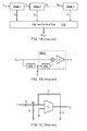
- FIG. 1A shows a conventional pipeline ADC.
- Several low resolution stages (Stage 1, 2, ... N) are cascaded to obtain high overall resolution.
- Each stage operates concurrently and performs coarse analog to digital conversion and computes its quantization error (as referred to as "residue").
- the quantization errors are factored into a data aligner and combiner 102, which outputs a digital signal D OUT .
- a disadvantage is that throughput is limited by the speed of a single stage.
- analog circuit non-idealities can be corrected by digital calibration.
- FIG. 1B is a block diagram of a single stage that may be used in the pipeline ADC of FIG. 1A .
- the stage includes an MDAC shown within dashed lines.
- the MDAC has a gain block G m (also referred to as an "inter-stage gain element") for improving noise, subsequent matching, and power dissipation in the pipeline ADC.
- G the active gain block
- FIG. 1C is a circuit diagram of a conventional MDAC.
- the residue gain is generated by an amplifier with transconductance G m , sample cap Ci, and capacitive feedback C F .
- Parasitics at the summing junction N3 are modeled by capacitor C p .
- Cp is typically on the order of the input sample capacitance C i , and may be much worse for split DAC capacitors and inter-leaving structures. Assuming load capacitance C L >> C F , the transfer function of the MDAC of FIG.
- F C f / (C f + C i + Cp)
- the present invention provides for an MDAC with improved efficiency.
- the amplifier includes a feed forward approach in which the input capacitor (also referred to as “sampling capacitor") is buffered by a common gate amplifier to improve bandwidth by removing input and parasitic capacitance terms (C i and Cp of FIG. 1C ) from the global feedback loss.
- local compensation is achieved by means of cascode compensation.
- the MDAC of the present invention has a feedback factor of about 1/3. This improves the bandwidth by at least 2.3 times for a gain of 4, and more for higher gain MDAC stages.
- the present invention relaxes the Gm, because the two poles are not inside the feedback loop and therefore, stability requirements for the two poles are relaxed.
- the MDAC bandwidth is improved by reducing the parasitic capacitance with a buffer at a cost of efficiency.
- FIG. 2 is a simplified circuit diagram of an MDAC 200 according to an embodiment of the present invention.
- the MDAC 200 may include an amplifier 202 with transconductance gm 2 , a common-gate amplifier 206, a current source 218, an input capacitor C i , and a feedback capacitor C f .
- the common-gate amplifier 206 may include an NMOS 214 and a current source 212.
- Parasitics at summing junction N3 in the circuit 210 are modeled by parasitic capacitor C p2 at the first input of the amplifier 202.
- the capacitance of the next stage (such as device and parasitic capacitance) and any self-loading in the devices of the current stage is modeled by load capacitor C L at the output of amplifier 202.
- the first current source 212 may be connected to a reference voltage and the drain of the NMOS 214.
- the current source 218 may be connected to the source of the NMOS 214.
- An input capacitor may be coupled to a node N1 joining the source of the NMOS 214 and the current source 218.
- a first input to the amplifier 202 may be connected to a node N2 joining the current source 212 and the drain of the NMOS 214.
- a second input of the amplifier may be connected to ground.
- a feedback capacitor C f may be coupled to the output of the amplifier 202 and the first input of the amplifier 202.
- a load capacitor C L may be coupled to the output of the amplifier 202 (at node N3).
- the common-gate amplifier buffers the input capacitor C i from the feedback capacitor C f , so that the MDAC gain gm2 is maintained, but the feedback factor (and hence, speed for a given power) is improved.
- the circuit 210 also has reduced C p2 compared to C p1 of the conventional MDAC.
- the circuit 210 has improved speed compared to the conventional MDAC of FIG. 1C
- FIG. 3A is a simplified circuit diagram of an MDAC according to an embodiment of the present invention.
- the MDAC 310 may include a first stage 340 and a second stage 360.
- the first stage 340 may include a common-gate amplifier 306, a current source 318, an input capacitor C i .
- the second stage may include a buffer 304, an amplifier 302, and a feedback capacitor C f .
- the common-gate amplifier 306 may include an NMOS 314 and a current source 312. Parasitics at summing junction N3 in the circuit 310 is modeled by parasitic capacitor C p3 at the input of the buffer 304.
- the capacitance of the next stage (such as device and parasitic capacitance) and any self-loading in the devices of the current stage is modeled by load capacitor C L at the output of amplifier 302.
- the components have the same functions and are connected in the same way as in FIG. 2 unless described elsewhere herein.
- the buffer 304 may be coupled between node N3 and the input of the amplifier 302.
- the current source 318 may be implemented with an NMOS, a resistor, or a combination of NMOSs and resistors.
- the circuit 310 has improved speed compared to the MDAC of FIG. 2 , because the buffer 304 can reduce the parasitic capacitance by an order of magnitude, that is C p3 « C p2 (equation given below). Thus, if C p3 ⁇ C f , the effect with C L is greatly reduced.
- the MDAC 350 of the FIG. 3B embodiment is a differential system.
- the system develops an analog residue output (V op and V on ) from the input signal V ip and V in .
- the input is quantized by a flash (not shown), then subtracted from the input signal and the remaining signal is Multiplied by the gain of the stage to produce the residue.
- the components of the MDAC 350 have the same functions and are connected in the same way as in FIG. 3A unless described elsewhere herein.
- the MDAC 350 may include a sample network 320 (also referred to as "DAC") for sampling an input signal, a first stage 340, and a second stage 360.
- the sample network 320 may sample an input signal that is then processed by the subsequent first stage 340 and second stage 360 to output an analog signal with components V on and V op .
- the first stage 340 may buffer sampling capacitors 332.1 and 332.2 to improve the feedback factor.
- the second stage buffers 364.1 and 364.2 buffer the parasitic input capacitance to gm2 to further improve efficiency.
- the capacitor C p3 366.1 and 366.2 may be smaller than the C p2 cap.
- the sample network 320 may include input switches 324.1 and 324.2, DAC switches 326.1 and 326.2, selection switches 328.1 and 328.1, a sampling switch 323, and sampling capacitors 332.1 and 332.2.
- Parasitic capacitance (as discussed above) is modeled as C p1 .
- Input switches 324.1 and 324.2 may connect input voltages to first terminals ("input terminals," for convenience) of sampling capacitors 332.1 and 332.2.
- Selection switches 328.1 and 328.2 may connect second terminals ("output terminals," for convenience) of sampling capacitors 332.1 and 332.2 nodes N2 and N4.
- the sampling switch 323 may connect the output terminals of the sampling capacitors 332.1 and 332.2 to each other.
- DAC switches 326.1 and 326.2 may connect input terminals of the sampling capacitors 332.1 and 332.2 to references voltages XV ref and YV ref .
- FIG. 3B also illustrates components of an exemplary first stage 340, which may include enhancement amplifiers 344.1 and 344.2, NMOSs 346.1, 346.2, 348.1 and 348.2, current sources 342.1 and 342.2, a common-mode controller 345, and a first clamp switch 343.
- FIG. 3B also illustrates components of an exemplary second stage 360, the MDAC 350 may include a second stage 360, which may include an amplifier 362, buffers 364.1 and 354.2, feedback capacitors (represented as C f ) and a second clamp switch 363.
- Parasitic capacitance (as discussed above) is modeled as C p3 and load capacitance (as discussed above) is modeled as C L .
- the second clamp switch 363 connects the feedback capacitors 372.1 and 372.2 to each other and the output of the amplifier 362.
- the common-mode controller 345 is coupled to the drains of NMOSs 348.1 348.2, and the first clamp switch 343 connects nodes N5 and N6 to each other.
- the MDAC 350 may operate in several phases of operation.
- input switches 324.1, 324.2, sampling switch 323, first clamp switch 343, and second clamp switch 363 may be closed such that input terminals of the sampling capacitors 332.1 and 332.2 are pulled to the input voltages V ip and V in , input terminals of the feedback capacitors 372.1 and 372.2 are substantially isolated from the effects of the sampling capacitors 332.1 and 332.2, and feedback capacitors 372.1 and 372.2 are at the same potential. This stores the input samples on the sampling capacitors 332.1 and 332.2 without affecting the feedback capacitors 372.1 and 372.2.
- the input switches 324.1, 324.2, sampling switch 323, first clamp switch 343, and second clamp switch 363 are then opened.
- DAC switches 326.1 and 326.2 are closed such that the input terminals of the sampling capacitors 332.1 and 332.2 are shorted to the appropriate quantized version of the input signal XV ref and YV ref that is provided by a flash (not shown).
- the selection switches 328.1 and 328.2 are then closed to allow the charge stored on the sampling capacitors 332.1 and 332.2 to be transferred to the feedback capacitors 372.1 and 372.2 to develop the output voltages V on and V op . Operation of the MDAC 350 may repeat for as long as desired.
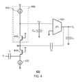
- FIG. 4 is a simplified circuit diagram of an MDAC 400 according to a further embodiment of the present invention.
- the components have the same functions and are connected in the same way as in FIG. 2 unless described elsewhere herein.
- the MDAC 400 may further include an NMOS 418.
- the source of the NMOS 418 may be connected to the source of the NMOS 416 and the current source 422 at node N4.
- the feedback capacitor C f may be used to cascade compensate a two-stage amplifier by being connected to the output of the amplifier 424 and node N4.
- the dominate pole is improved by removal of the +1 term in the effective capacitance (see equation below).
- the cascode is real, performance is improved if its bandwidth is far from the dominate pole.
- C eff C p ⁇ 2 + C L C p ⁇ 2 C f
- FIG. 5 is a simplified circuit diagram of an MDAC 500 according to a further embodiment of the present invention.
- the components have the same functions and are connected in the same way as in FIG. 4 unless described elsewhere herein.
- the MDAC 500 may further include a buffer 526.
- An input of buffer 526 is connected to the node N3 and an input of the buffer 526 is connected to the input of the amplifier 524.
- the circuit 500 has improved speed compared to the MDAC of FIG. 4 , because C p3 ⁇ C p2 .
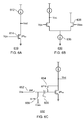
- FIGs. 6A-6C are simplified circuit diagrams of enhancement amplifiers 610, 630, and 650 according to an embodiment of the present invention. They may each be used as the first stage amplifier in an MDAC (such as the amplifiers 344.1 and 344.2 shown in FIG. 3B ).
- the enhancement amplifier 610 may include a current source 612 connected to the drain of an NMOS 614.
- the enhancement amplifier 630 may include the same components as the enhancement amplifier 610, and may further include a second NMOS 638 and a second current source 636 that connects the sources of the NMOSs 634 and 638.
- the gate of the NMOS 638 may be connected to a bias voltage V bias .
- the enhancement amplifier 630 may be advantageously designed such that V gs is decoupled from setting the DC voltage at V ipa .
- the enhancement amplifier 650 may include the same components as the enhancement amplifier 610, and may further include a selection switch 652, a first clamp switch 656, a second clamp switch 654, and a capacitor 658 such that the offset of the device Gm ea is auto-zeroed in the clamp phase.
- the enhancement amplifier 650 may be advantageously designed to have lower offset.
- An enhancement amplifier may also be designed to be a combination of the enhancement amplifier 630 and the enhancement amplifier 650 (not shown) to advantageously have even less offset.
- FIGs. 7A and 7B are simplified circuit diagrams of buffers 710 and 730 according to an embodiment of the present invention. They may each be used as the second stage buffer in an MDAC (such as the buffers 364.1 and 364.2 shown in FIG. 3B ).
- the buffer 710 may be an NMOS follower having an NMOS 712 and a current source 714 connected to the source of the NMOS 712.
- the buffer 730 may include the same components as the buffer 710, and may further include a capacitor 716 and a clamp switch 718 to have a DC level shift.
- the capacitor 716 and the clamp switch 718 may each be connected to the gate of the NMOS.
- FIG. 8 is a simplified circuit diagram of an amplifier 800 according to an embodiment of the present invention that may be used as the second stage amplifier in an MDAC (such as the amplifier 362 shown in FIG. 3B ).
- the amplifier 800 may be a common-source differential pair with cascodes to increase gain.
- the amplifier 800 may include a common mode control 822 and NMOSs 816, 818, 836, and 838.
- the common mode control 822 may be implemented by a clicker circuit.
- the amplifier may advantageously designed to further include current sources 812 and 832. These current sources improve gm2 (818/838) without the penalty of self-loading the output of the amplifier by increasing the cascode devices (816/836) unnecessarily.
- NMOSs may be implemented with PMOSs or other transistors in the embodiments described above. Modifications, variations, and improvements are possible in light of the teachings above and the claims below, and are intended to be within the spirit and scope of the invention.
Landscapes
- Engineering & Computer Science (AREA)
- Power Engineering (AREA)
- Theoretical Computer Science (AREA)
- Amplifiers (AREA)
Abstract
Description
- The present invention relates to amplifiers, more specifically it relates to improving speed and power in a switched-capacitor amplifier such as a multiplying digital-to-analog converter (MDAC).
- Analog-to-digital converters (ADCs) are used in electronic devices to convert an analog signal to a digital signal. ADCs can be designed in a number of different architectures. One conventional ADC architecture is the pipeline ADC. A pipeline ADC, as illustrated in
FIG. 1A , operates on discrete time signals, and therefore mathematical operations, sample-and-hold, DAC, and gain can all be performed in a single switched-capacitor circuit such as an MDAC. An MDAC is a high-gain and high-bandwidth amplifier with capacitive feedback. - In analog design, it is ideal to minimize power consumed and maximize speed. However, in modern high speed switched-capacitor CMOS pipeline ADCs, the MDAC is a major contributor in power consumption and limitation of clock rate. Current architectures of MDAC amplifiers, whether single- or multi-stage, have inherently limited efficiency because loop-gain is attenuated by significant loss in the feedback, in part due to significant parasitic capacitors on the summation node (such as node N3 of
FIG. 1C ). If the loop-gain can be increased with a topology change or reduction of the parasitic capacitance, then a more efficient amplifier can be built where settling time is reduced (increased bandwidth) and power can be minimized. - Conventional techniques have limitations in the settling response due to non-dominate poles. In addition, these non-dominate poles are typically inside a global feedback loop with a sampling capacitor and a feedback capacitor, which greatly increases the sensitivity of the system and the difficulty of controlling the system. Thus, there also exists a need to reduce the sensitivity of the system and improve the stability of the system, for example by removing the poles from inside the feedback loop.
- The present invention provides for an MDAC that reduces the power consumption of the MDAC by at least 2.3 times by eliminating the global feedback and improving the local feedback factor. In a first embodiment, the amplifier includes a feed forward approach in which the input capacitor (also referred to as "sampling capacitor") is buffered by a common gate amplifier to improve bandwidth by removing input and parasitic capacitance terms from the global feedback loss. In a second embodiment, which may incorporate the same features as the first embodiment, local compensation is achieved by means of cascode compensation. In a third embodiment, which may incorporate the same features as the first and second embodiments, the bandwidth is improved by reducing the parasitic capacitance with a buffer.
-
-
FIG. 1A shows a conventional pipeline ADC. -
FIG. 1B is a block diagram of a conventional MDAC that may be used in the pipeline ADC ofFIG. 1A . -
FIG. 1C is a circuit diagram of a conventional MDAC. -
FIG. 2 is a simplified circuit diagram of an MDAC according to an embodiment of the present invention. -
FIG. 3A is a simplified circuit diagram of an MDAC having a buffered input capacitor according to an embodiment of the present invention. -
FIG. 3B is a simplified circuit diagram of a differential MDAC according to an embodiment of the present invention. -
FIG. 4 is a simplified circuit diagram of an MDAC having cascode compensation according to an embodiment of the present invention. -
FIG. 5 is a simplified circuit diagram of an MDAC having cascode compensation and a second stage buffer according to an embodiment of the present invention. -
FIG. 6A is a simplified circuit diagram of an enhancement amplifier of an MDAC according to an embodiment of the present invention. -
FIG. 6B is a simplified circuit diagram of an enhancement amplifier of an MDAC according to an embodiment of the present invention. -
FIG. 6C is a simplified circuit diagram of an enhancement amplifier of an MDAC according to an embodiment of the present invention. -
FIG. 7A is a circuit diagram of an NMOS follower than can be used as the stage two buffer in an MDAC according to an embodiment of the present invention. -
FIG. 7B is a simplified circuit diagram of a second stage buffer in an MDAC according to an embodiment of the present invention. -
FIG. 8 is a simplified circuit diagram of a second stage amplifier in an MDAC according to an embodiment of the present invention. -
FIG. 1A shows a conventional pipeline ADC. Several low resolution stages (Stage -
FIG. 1B is a block diagram of a single stage that may be used in the pipeline ADC ofFIG. 1A . The stage includes an MDAC shown within dashed lines. The MDAC has a gain block Gm (also referred to as an "inter-stage gain element") for improving noise, subsequent matching, and power dissipation in the pipeline ADC. However, as discussed above, G (the active gain block) is a major contributor to power consumption and limitation of clock rate. -
FIG. 1C is a circuit diagram of a conventional MDAC. In conventional architectures, the residue gain is generated by an amplifier with transconductance Gm, sample cap Ci, and capacitive feedback CF. Parasitics at the summing junction N3 are modeled by capacitor Cp. Cp is typically on the order of the input sample capacitance Ci, and may be much worse for split DAC capacitors and inter-leaving structures. Assuming load capacitance CL >> CF, the transfer function of the MDAC ofFIG. 1C is represented by:


- There is a penalty to bandwidth, because the feedback factor is given by the ratio of the feedback capacitance to the sum of all capacitances, i.e., F = Cf/ (Cf + Ci + Cp) For example, when there is a gain of 4 in the MDAC stage (2.5-bit stage), the feedback factor is approximately 1/7. For example, if there is a gain of 8, the feedback factor degrades more.
- The present invention provides for an MDAC with improved efficiency. In an embodiment, the amplifier includes a feed forward approach in which the input capacitor (also referred to as "sampling capacitor") is buffered by a common gate amplifier to improve bandwidth by removing input and parasitic capacitance terms (Ci and Cp of
FIG. 1C ) from the global feedback loss. In another embodiment, local compensation is achieved by means of cascode compensation. The MDAC of the present invention has a feedback factor of about 1/3. This improves the bandwidth by at least 2.3 times for a gain of 4, and more for higher gain MDAC stages. As contrasted with the Gm of conventional designs in which the second stage's non-dominate pole is placed three to four times beyond the dominate pole, the present invention relaxes the Gm, because the two poles are not inside the feedback loop and therefore, stability requirements for the two poles are relaxed. In a third embodiment, the MDAC bandwidth is improved by reducing the parasitic capacitance with a buffer at a cost of efficiency. -
FIG. 2 is a simplified circuit diagram of anMDAC 200 according to an embodiment of the present invention. TheMDAC 200 may include anamplifier 202 with transconductance gm2, acommon-gate amplifier 206, acurrent source 218, an input capacitor Ci, and a feedback capacitor Cf. Thecommon-gate amplifier 206 may include anNMOS 214 and acurrent source 212. Parasitics at summing junction N3 in the circuit 210 are modeled by parasitic capacitor Cp2 at the first input of theamplifier 202. The capacitance of the next stage (such as device and parasitic capacitance) and any self-loading in the devices of the current stage is modeled by load capacitor CL at the output ofamplifier 202. The firstcurrent source 212 may be connected to a reference voltage and the drain of theNMOS 214. Thecurrent source 218 may be connected to the source of theNMOS 214. An input capacitor may be coupled to a node N1 joining the source of theNMOS 214 and thecurrent source 218. A first input to theamplifier 202 may be connected to a node N2 joining thecurrent source 212 and the drain of theNMOS 214. A second input of the amplifier may be connected to ground. A feedback capacitor Cf may be coupled to the output of theamplifier 202 and the first input of theamplifier 202. A load capacitor CL may be coupled to the output of the amplifier 202 (at node N3). In operation, the common-gate amplifier buffers the input capacitor Ci from the feedback capacitor Cf, so that the MDAC gain gm2 is maintained, but the feedback factor (and hence, speed for a given power) is improved. - The feedback factor is improved, because effective capacitance does not contain input capacitance (equation given below). The circuit 210 also has reduced Cp2 compared to Cp1 of the conventional MDAC. The transfer function for the MDAC of
FIG. 2A is represented by:


FIG. 1C -
FIG. 3A is a simplified circuit diagram of an MDAC according to an embodiment of the present invention. TheMDAC 310 may include afirst stage 340 and asecond stage 360. Thefirst stage 340 may include acommon-gate amplifier 306, acurrent source 318, an input capacitor Ci. The second stage may include abuffer 304, anamplifier 302, and a feedback capacitor Cf. Thecommon-gate amplifier 306 may include anNMOS 314 and acurrent source 312. Parasitics at summing junction N3 in thecircuit 310 is modeled by parasitic capacitor Cp3 at the input of thebuffer 304. The capacitance of the next stage (such as device and parasitic capacitance) and any self-loading in the devices of the current stage is modeled by load capacitor CL at the output ofamplifier 302. The components have the same functions and are connected in the same way as inFIG. 2 unless described elsewhere herein. Thebuffer 304 may be coupled between node N3 and the input of theamplifier 302. Thecurrent source 318 may be implemented with an NMOS, a resistor, or a combination of NMOSs and resistors. - The
circuit 310 has improved speed compared to the MDAC ofFIG. 2 , because thebuffer 304 can reduce the parasitic capacitance by an order of magnitude, that is Cp3 « Cp2 (equation given below). Thus, if Cp3 < Cf, the effect with CL is greatly reduced. The transfer function for the MDAC ofFIG. 3A is represented by:


- The
MDAC 350 of theFIG. 3B embodiment is a differential system. The system develops an analog residue output (Vop and Von) from the input signal Vip and Vin. The input is quantized by a flash (not shown), then subtracted from the input signal and the remaining signal is Multiplied by the gain of the stage to produce the residue. The components of theMDAC 350 have the same functions and are connected in the same way as inFIG. 3A unless described elsewhere herein. TheMDAC 350 may include a sample network 320 (also referred to as "DAC") for sampling an input signal, afirst stage 340, and asecond stage 360. Thesample network 320 may sample an input signal that is then processed by the subsequentfirst stage 340 andsecond stage 360 to output an analog signal with components Von and Vop. Thefirst stage 340 may buffer sampling capacitors 332.1 and 332.2 to improve the feedback factor. The second stage buffers 364.1 and 364.2 buffer the parasitic input capacitance to gm2 to further improve efficiency. The capacitor Cp3 366.1 and 366.2 may be smaller than the Cp2 cap. - In an embodiment, the
sample network 320 may include input switches 324.1 and 324.2, DAC switches 326.1 and 326.2, selection switches 328.1 and 328.1, asampling switch 323, and sampling capacitors 332.1 and 332.2. Parasitic capacitance (as discussed above) is modeled as Cp1. Input switches 324.1 and 324.2 may connect input voltages to first terminals ("input terminals," for convenience) of sampling capacitors 332.1 and 332.2. Selection switches 328.1 and 328.2 may connect second terminals ("output terminals," for convenience) of sampling capacitors 332.1 and 332.2 nodes N2 and N4. Thesampling switch 323 may connect the output terminals of the sampling capacitors 332.1 and 332.2 to each other. DAC switches 326.1 and 326.2 may connect input terminals of the sampling capacitors 332.1 and 332.2 to references voltages XVref and YVref. -
FIG. 3B also illustrates components of an exemplaryfirst stage 340, which may include enhancement amplifiers 344.1 and 344.2, NMOSs 346.1, 346.2, 348.1 and 348.2, current sources 342.1 and 342.2, a common-mode controller 345, and a first clamp switch 343.FIG. 3B also illustrates components of an exemplarysecond stage 360, theMDAC 350 may include asecond stage 360, which may include anamplifier 362, buffers 364.1 and 354.2, feedback capacitors (represented as Cf) and asecond clamp switch 363. Parasitic capacitance (as discussed above) is modeled as Cp3 and load capacitance (as discussed above) is modeled as CL. Thesecond clamp switch 363 connects the feedback capacitors 372.1 and 372.2 to each other and the output of theamplifier 362. In a further embodiment, in thefirst stage 340, the common-mode controller 345 is coupled to the drains of NMOSs 348.1 348.2, and the first clamp switch 343 connects nodes N5 and N6 to each other. - The
MDAC 350 may operate in several phases of operation. During a clamp/acquire phase, input switches 324.1, 324.2,sampling switch 323, first clamp switch 343, andsecond clamp switch 363 may be closed such that input terminals of the sampling capacitors 332.1 and 332.2 are pulled to the input voltages Vip and Vin, input terminals of the feedback capacitors 372.1 and 372.2 are substantially isolated from the effects of the sampling capacitors 332.1 and 332.2, and feedback capacitors 372.1 and 372.2 are at the same potential. This stores the input samples on the sampling capacitors 332.1 and 332.2 without affecting the feedback capacitors 372.1 and 372.2. The input switches 324.1, 324.2,sampling switch 323, first clamp switch 343, andsecond clamp switch 363 are then opened. During a gain (also referred to as a hold or amplify) phase, DAC switches 326.1 and 326.2 are closed such that the input terminals of the sampling capacitors 332.1 and 332.2 are shorted to the appropriate quantized version of the input signal XVref and YVref that is provided by a flash (not shown). The selection switches 328.1 and 328.2 are then closed to allow the charge stored on the sampling capacitors 332.1 and 332.2 to be transferred to the feedback capacitors 372.1 and 372.2 to develop the output voltages Von and Vop. Operation of theMDAC 350 may repeat for as long as desired. -
FIG. 4 is a simplified circuit diagram of anMDAC 400 according to a further embodiment of the present invention. The components have the same functions and are connected in the same way as inFIG. 2 unless described elsewhere herein. TheMDAC 400 may further include an NMOS 418. The source of the NMOS 418 may be connected to the source of the NMOS 416 and thecurrent source 422 at node N4. As contrasted withFIG. 3A , the feedback capacitor Cf may be used to cascade compensate a two-stage amplifier by being connected to the output of theamplifier 424 and node N4. - In the ideal case in which the cascode buffer is ideal, the dominate pole is improved by removal of the +1 term in the effective capacitance (see equation below). When the cascode is real, performance is improved if its bandwidth is far from the dominate pole. The transfer function for the
MDAC 400 ofFIG. 4 is represented by: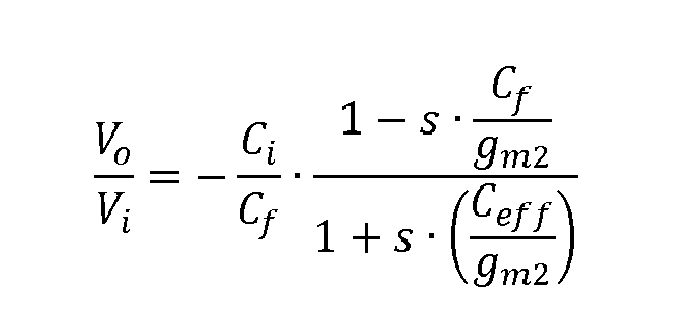


-
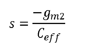
FIG. 5 is a simplified circuit diagram of anMDAC 500 according to a further embodiment of the present invention. The components have the same functions and are connected in the same way as inFIG. 4 unless described elsewhere herein. TheMDAC 500 may further include abuffer 526. An input ofbuffer 526 is connected to the node N3 and an input of thebuffer 526 is connected to the input of theamplifier 524. - The
circuit 500 has improved speed compared to the MDAC ofFIG. 4 , because Cp3 << Cp2. The transfer function for theMDAC 500 ofFIG. 5 is represented by:

-
FIGs. 6A-6C are simplified circuit diagrams ofenhancement amplifiers FIG. 3B ). The enhancement amplifier 610 may include acurrent source 612 connected to the drain of anNMOS 614. Theenhancement amplifier 630 may include the same components as the enhancement amplifier 610, and may further include asecond NMOS 638 and a secondcurrent source 636 that connects the sources of theNMOSs 634 and 638. The gate of theNMOS 638 may be connected to a bias voltage Vbias. Theenhancement amplifier 630 may be advantageously designed such that Vgs is decoupled from setting the DC voltage at Vipa. Theenhancement amplifier 650 may include the same components as the enhancement amplifier 610, and may further include aselection switch 652, afirst clamp switch 656, asecond clamp switch 654, and acapacitor 658 such that the offset of the device Gmea is auto-zeroed in the clamp phase. Theenhancement amplifier 650 may be advantageously designed to have lower offset. An enhancement amplifier may also be designed to be a combination of theenhancement amplifier 630 and the enhancement amplifier 650 (not shown) to advantageously have even less offset. -
FIGs. 7A and 7B are simplified circuit diagrams ofbuffers FIG. 3B ). Thebuffer 710 may be an NMOS follower having anNMOS 712 and acurrent source 714 connected to the source of theNMOS 712. Thebuffer 730 may include the same components as thebuffer 710, and may further include acapacitor 716 and aclamp switch 718 to have a DC level shift. Thecapacitor 716 and theclamp switch 718 may each be connected to the gate of the NMOS. -
FIG. 8 is a simplified circuit diagram of anamplifier 800 according to an embodiment of the present invention that may be used as the second stage amplifier in an MDAC (such as theamplifier 362 shown inFIG. 3B ). Theamplifier 800 may be a common-source differential pair with cascodes to increase gain. Theamplifier 800 may include acommon mode control 822 andNMOSs common mode control 822 may be implemented by a clicker circuit. In another embodiment, the amplifier may advantageously designed to further includecurrent sources - The descriptions and illustrations of the embodiments above should be read as exemplary and not limiting. For example, NMOSs may be implemented with PMOSs or other transistors in the embodiments described above. Modifications, variations, and improvements are possible in light of the teachings above and the claims below, and are intended to be within the spirit and scope of the invention.
Claims (15)
- A method for improving the efficiency of a switched-capacitor amplifier having a sampling capacitor and a feedback capacitor, the method comprising:buffering the sampling capacitor from the feedback capacitor such that a gain of the amplifier is maintained and a feedback factor of the amplifier is increased by removing a capacitance of the sampling capacitor from the feedback factor.
- The method of claim 1, wherein at least one of the following applies:a) the method further comprises performing a cascode compensation;b) the method further comprises reducing a parasitic capacitance by using a buffer.
- The method of claim 1 or 2, wherein the feedback factor is a ratio of a capacitance of the feedback capacitor to the sum of: the capacitance of the feedback capacitor and a parasitic capacitance.
- The method of any preceding claim wherein the switched-capacitor amplifier has an input switch coupled to the sampling capacitor, a DAC switch coupled to the sampling capacitor and a reference voltage, a selection switch coupled to the sampling capacitor, a sampling switch coupled to the selection switch and the sampling capacitor, and a clamp switch coupled to the feedback capacitor, the method comprising:closing the input switch, the sampling switch, and the clamp switch in a first mode of operation;opening the input switch, the sampling switch, and the clamp switch in a second mode of operation; andclosing the DAC switch and the selection switch in the second mode of operation.
- A multiplying digital-to-analog converter comprising:a first stage including:an input capacitor coupled to an input of the multiplying digital-to-analog converter; anda common-gate amplifier coupled to the input capacitor and a first current source; anda second stage coupled to an output of the first stage, the second stage including:an amplifier having an input coupled to an intermediate node of the common-gate amplifier; anda feedback capacitor coupled to the input of the amplifier and an output of the amplifier.
- The multiplying digital-to-analog converter according to claim 5, wherein the common-gate amplifier includes:an NMOS having a drain connected to a second current source and a source connected to the first current source.
- The multiplying digital-to-analog converter according to claim 5, further comprising:an NMOS having a drain connected to the common-gate amplifier; andan enhancement amplifier having an output connected to a gate of the NMOS and an input connected to a source of the NMOS and the first current source.
- The multiplying digital-to-analog converter according to claim 5 or 7, further comprising a buffer coupled to the intermediate node of the common-gate amplifier and the input of the amplifier.
- A multiplying digital-to-analog converter comprising:a first stage including:an input capacitor coupled to an input of the multiplying digital-to-analog converter;a common-gate amplifier coupled to the NMOS; andan NMOS having a drain coupled to the common-gate amplifier, and a source coupled to a first current source; anda second stage coupled to an output of the first stage, the second stage including:an amplifier having an input coupled to an intermediate node of the common-gate amplifier; anda feedback capacitor having an input coupled to the common-gate amplifier and the drain of the NMOS, and an output coupled to an output of the amplifier.
- The multiplying digital-to-analog converter according to claim 9, further comprising a buffer coupled to the intermediate node of the common-gate amplifier and the input of the amplifier.
- The multiplying digital-to-analog converter according to claim 8 when dependent on claim 7, further comprising:a sample network including:at least one input switch connected to the input of the multiplying digital-to-analog converter and the input capacitor;at least one selection switch connected to the input capacitor and an input to the first stage;at least one DAC switch connected to the input capacitor and a reference voltage;a sample switch connected to the input capacitor and the at least one selection switch; anda first clamp switch connected to the output of the first stage and the input of the second stage;wherein the first stage further includes a common-mode controller connected to the output of the common-gate amplifier and the output of the first stage ; andthe second stage further includes a second clamp switch connected to the output of the amplifier.
- The multiplying digital-to-analog converter according to claim 11, wherein at least one of the following appliesa) the enhancement amplifier includes:a first NMOS having a gate coupled to the input of the multiplying digital-to-analog converter and having a source;a second NMOS having a source coupled to the source of the first NMOS and having a gate connected to a bias voltage;a first current source coupled to a drain of the first NMOS; anda second current source coupled to the respective sources of the first NMOS and the second NMOS.b) the enhancement amplifier includes:a current source;an NMOS having a drain coupled to the current source;a selection switch connected to the input of the multiplying digital-to-analog converter;a first clamp switch connected to the gate and the drain of the NMOS;a second clamp switch connected to a bias voltage;a capacitor having a first terminal connected to the second clamp switch and the gate of the NMOS, and a second terminal connected to the selection switch and the first clamp switch.
- The multiplying digital-to-analog converter according to claim 11, wherein the buffer includes:an NMOS;a current source connected to a source of the NMOS;a capacitor connected to the gate of the NMOS; anda clamp switch connected to the capacitor and a bias voltage.
- The multiplying digital-to-analog converter according to claim 11, wherein the amplifier of the second stage includes:a common-mode controller;a first current source having a first terminal and a second terminal;a second current source having a first terminal coupled to the first terminal of the first current source;a first NMOS having a drain connected to the second terminal of the first current source;a second NMOS having a drain connected to the second terminal of the second current source;a third NMOS having a drain connected to the source of the first NMOS and a source connected to the common-mode controller; anda fourth NMOS having a drain connected to the source of the second NMOS and a source connected to the common-mode controller.
- The multiplying digital-to-analog converter according to claim 11, wherein the amplifier of the second stage further includes:a third current source having a first terminal coupled to the respective first terminals of the first and the second current sources, and a second terminal coupled to a node joining the source of the first NMOS and the drain of the third NMOS; anda fourth current source having a first terminal coupled to the respective first terminals of the first, the second, and the third current sources, and a second terminal coupled to a node joining the source of the second NMOS and the drain of the fourth NMOS.
Applications Claiming Priority (1)
| Application Number | Priority Date | Filing Date | Title |
|---|---|---|---|
| US13/801,317 US8803721B1 (en) | 2013-03-13 | 2013-03-13 | System and method for improving speed and power in a switched-capacitor amplifier |
Publications (2)
| Publication Number | Publication Date |
|---|---|
| EP2779465A2 true EP2779465A2 (en) | 2014-09-17 |
| EP2779465A3 EP2779465A3 (en) | 2014-11-05 |
Family
ID=50189599
Family Applications (1)
| Application Number | Title | Priority Date | Filing Date |
|---|---|---|---|
| EP14157515.9A Withdrawn EP2779465A3 (en) | 2013-03-13 | 2014-03-03 | System and method for improving speed and power in a switched capacitor amplifier |
Country Status (3)
| Country | Link |
|---|---|
| US (1) | US8803721B1 (en) |
| EP (1) | EP2779465A3 (en) |
| CN (1) | CN104052475B (en) |
Families Citing this family (5)
| Publication number | Priority date | Publication date | Assignee | Title |
|---|---|---|---|---|
| US9276468B2 (en) | 2013-08-13 | 2016-03-01 | Analog Devices, Inc. | Low-noise current source |
| EP3480949A1 (en) * | 2017-11-06 | 2019-05-08 | IMEC vzw | Multiplying digital-to-analog conversion circuit |
| US10541702B1 (en) * | 2018-09-26 | 2020-01-21 | Analog Devices Global Unlimited Company | Auxiliary input for analog-to-digital converter input charge |
| US10854306B1 (en) | 2019-09-19 | 2020-12-01 | Analog Devices, Inc. | Common-gate comparator and fuse reader |
| EP3806334B1 (en) * | 2019-10-07 | 2023-08-30 | IniVation AG | Switched capacitor circuit |
Family Cites Families (9)
| Publication number | Priority date | Publication date | Assignee | Title |
|---|---|---|---|---|
| CN1275392C (en) * | 2002-06-18 | 2006-09-13 | 模拟设备股份有限公司 | Switched capacitor stage and pipelined analog-to-digital converter |
| US7012463B2 (en) | 2003-12-23 | 2006-03-14 | Analog Devices, Inc. | Switched capacitor circuit with reduced common-mode variations |
| US7157955B2 (en) * | 2004-12-03 | 2007-01-02 | Silicon Laboratories, Inc. | Switched capacitor sampler circuit and method therefor |
| CN100386964C (en) * | 2005-03-04 | 2008-05-07 | 清华大学 | AC Powered Amplifiers in Switched Capacitor Circuits |
| US7279986B2 (en) * | 2005-05-23 | 2007-10-09 | Analog Devices, Inc. | Buffer amplifiers with enhanced efficiency |
| US7639073B2 (en) * | 2007-11-16 | 2009-12-29 | Omnivision Technologies, Inc. | Switched-capacitor amplifier with improved reset phase |
| CN101364800B (en) * | 2008-09-26 | 2011-09-14 | 海芯科技(厦门)有限公司 | Low noise switch capacitor circuit having embedded amplifier |
| US7889004B1 (en) | 2009-09-30 | 2011-02-15 | Analog Devices, Inc. | Operational amplifiers with enhanced parameters |
| US8018274B1 (en) * | 2010-03-12 | 2011-09-13 | Maxim Integrated Products, Inc. | Switched capacitor amplifier circuit with clamping |
-
2013
- 2013-03-13 US US13/801,317 patent/US8803721B1/en active Active
-
2014
- 2014-03-03 EP EP14157515.9A patent/EP2779465A3/en not_active Withdrawn
- 2014-03-13 CN CN201410091523.1A patent/CN104052475B/en active Active
Non-Patent Citations (1)
| Title |
|---|
| None |
Also Published As
| Publication number | Publication date |
|---|---|
| CN104052475B (en) | 2019-01-22 |
| EP2779465A3 (en) | 2014-11-05 |
| CN104052475A (en) | 2014-09-17 |
| US8803721B1 (en) | 2014-08-12 |
Similar Documents
| Publication | Publication Date | Title |
|---|---|---|
| US7903017B2 (en) | Comparator for a pipelined analog-to-digital converter and related signal sampling method | |
| US5963156A (en) | Sample and hold circuit and method with common mode differential signal feedback for converting single-ended signals to differential signals | |
| US7525383B2 (en) | Differential amplifier | |
| US9667194B2 (en) | Differential switched capacitor circuits having voltage amplifiers, and associated methods | |
| US9214912B2 (en) | Switched capacitor circuits having level-shifting buffer amplifiers, and associated methods | |
| US7924206B2 (en) | Switched capacitor circuit and pipeline A/D converter | |
| EP2220764B1 (en) | Switched-capacitor amplifier with improved reset phase | |
| US7868810B2 (en) | Amplifier circuit and A/D converter | |
| US9077356B2 (en) | MDAC with differential current cancellation | |
| US8803721B1 (en) | System and method for improving speed and power in a switched-capacitor amplifier | |
| JP2002074976A (en) | Sample hold amplifier circuit, pipeline type AD converter using the same, and pipeline type DA converter | |
| US8299952B1 (en) | Switched-capacitor circuit and pipelined analog-to-digital converter | |
| US20040021511A1 (en) | Amplifier common-mode feedback systems for use with switched-capacitor structures | |
| US6954169B1 (en) | 1/f noise, offset-voltage charge injection induced error cancelled op-amp sharing technique | |
| EP1315290B1 (en) | Pseudo-differential amplifier and analog-to-digital converter using the same | |
| US7382305B1 (en) | Reference generators for enhanced signal converter accuracy | |
| US6611163B1 (en) | Switched capacitor scheme for offset compensated comparators | |
| US7405625B1 (en) | Common-mode control structures and signal converter systems for use therewith | |
| US7034737B1 (en) | Switched capacitor circuits | |
| CN109075755B (en) | Distance sensor receiving analog front-end circuit and distance sensor | |
| US20060125674A1 (en) | Efficient Amplifier Sharing in a Multi-stage Analog to Digital Converter | |
| CN101964661B (en) | Comparator and Related Signal Sampling Method for Pipeline Analog-to-Digital Converter | |
| US20220158649A1 (en) | Control circuit of pipeline ADC | |
| US20110291873A1 (en) | Differential amplifier and pipeline a/d converter using the same | |
| US10574255B2 (en) | Multiplying digital-to-analog conversion circuit |
Legal Events
| Date | Code | Title | Description |
|---|---|---|---|
| PUAI | Public reference made under article 153(3) epc to a published international application that has entered the european phase |
Free format text: ORIGINAL CODE: 0009012 |
|
| 17P | Request for examination filed |
Effective date: 20140303 |
|
| AK | Designated contracting states |
Kind code of ref document: A2 Designated state(s): AL AT BE BG CH CY CZ DE DK EE ES FI FR GB GR HR HU IE IS IT LI LT LU LV MC MK MT NL NO PL PT RO RS SE SI SK SM TR |
|
| AX | Request for extension of the european patent |
Extension state: BA ME |
|
| PUAL | Search report despatched |
Free format text: ORIGINAL CODE: 0009013 |
|
| AK | Designated contracting states |
Kind code of ref document: A3 Designated state(s): AL AT BE BG CH CY CZ DE DK EE ES FI FR GB GR HR HU IE IS IT LI LT LU LV MC MK MT NL NO PL PT RO RS SE SI SK SM TR |
|
| AX | Request for extension of the european patent |
Extension state: BA ME |
|
| RIC1 | Information provided on ipc code assigned before grant |
Ipc: H03M 1/16 20060101AFI20141002BHEP |
|
| R17P | Request for examination filed (corrected) |
Effective date: 20150505 |
|
| RBV | Designated contracting states (corrected) |
Designated state(s): AL AT BE BG CH CY CZ DE DK EE ES FI FR GB GR HR HU IE IS IT LI LT LU LV MC MK MT NL NO PL PT RO RS SE SI SK SM TR |
|
| STAA | Information on the status of an ep patent application or granted ep patent |
Free format text: STATUS: EXAMINATION IS IN PROGRESS |
|
| 17Q | First examination report despatched |
Effective date: 20170329 |
|
| STAA | Information on the status of an ep patent application or granted ep patent |
Free format text: STATUS: THE APPLICATION HAS BEEN WITHDRAWN |
|
| 18W | Application withdrawn |
Effective date: 20200602 |