EP2779391A1 - Active front end power converter with boost mode derating to protect filter inductor - Google Patents
Active front end power converter with boost mode derating to protect filter inductor Download PDFInfo
- Publication number
- EP2779391A1 EP2779391A1 EP14160229.2A EP14160229A EP2779391A1 EP 2779391 A1 EP2779391 A1 EP 2779391A1 EP 14160229 A EP14160229 A EP 14160229A EP 2779391 A1 EP2779391 A1 EP 2779391A1
- Authority
- EP
- European Patent Office
- Prior art keywords
- output current
- rectifier
- line
- current value
- bus voltage
- Prior art date
- Legal status (The legal status is an assumption and is not a legal conclusion. Google has not performed a legal analysis and makes no representation as to the accuracy of the status listed.)
- Granted
Links
Images



Classifications
-
- H—ELECTRICITY
- H02—GENERATION; CONVERSION OR DISTRIBUTION OF ELECTRIC POWER
- H02M—APPARATUS FOR CONVERSION BETWEEN AC AND AC, BETWEEN AC AND DC, OR BETWEEN DC AND DC, AND FOR USE WITH MAINS OR SIMILAR POWER SUPPLY SYSTEMS; CONVERSION OF DC OR AC INPUT POWER INTO SURGE OUTPUT POWER; CONTROL OR REGULATION THEREOF
- H02M7/00—Conversion of AC power input into DC power output; Conversion of DC power input into AC power output
- H02M7/02—Conversion of AC power input into DC power output without possibility of reversal
- H02M7/04—Conversion of AC power input into DC power output without possibility of reversal by static converters
- H02M7/12—Conversion of AC power input into DC power output without possibility of reversal by static converters using discharge tubes with control electrode or semiconductor devices with control electrode
- H02M7/21—Conversion of AC power input into DC power output without possibility of reversal by static converters using discharge tubes with control electrode or semiconductor devices with control electrode using devices of a triode or transistor type requiring continuous application of a control signal
- H02M7/217—Conversion of AC power input into DC power output without possibility of reversal by static converters using discharge tubes with control electrode or semiconductor devices with control electrode using devices of a triode or transistor type requiring continuous application of a control signal using semiconductor devices only
-
- H—ELECTRICITY
- H02—GENERATION; CONVERSION OR DISTRIBUTION OF ELECTRIC POWER
- H02M—APPARATUS FOR CONVERSION BETWEEN AC AND AC, BETWEEN AC AND DC, OR BETWEEN DC AND DC, AND FOR USE WITH MAINS OR SIMILAR POWER SUPPLY SYSTEMS; CONVERSION OF DC OR AC INPUT POWER INTO SURGE OUTPUT POWER; CONTROL OR REGULATION THEREOF
- H02M1/00—Details of apparatus for conversion
- H02M1/32—Means for protecting converters other than automatic disconnection
-
- H—ELECTRICITY
- H02—GENERATION; CONVERSION OR DISTRIBUTION OF ELECTRIC POWER
- H02M—APPARATUS FOR CONVERSION BETWEEN AC AND AC, BETWEEN AC AND DC, OR BETWEEN DC AND DC, AND FOR USE WITH MAINS OR SIMILAR POWER SUPPLY SYSTEMS; CONVERSION OF DC OR AC INPUT POWER INTO SURGE OUTPUT POWER; CONTROL OR REGULATION THEREOF
- H02M1/00—Details of apparatus for conversion
- H02M1/42—Circuits or arrangements for compensating for or adjusting power factor in converters or inverters
- H02M1/4208—Arrangements for improving power factor of AC input
- H02M1/4216—Arrangements for improving power factor of AC input operating from a three-phase input voltage
-
- H—ELECTRICITY
- H02—GENERATION; CONVERSION OR DISTRIBUTION OF ELECTRIC POWER
- H02M—APPARATUS FOR CONVERSION BETWEEN AC AND AC, BETWEEN AC AND DC, OR BETWEEN DC AND DC, AND FOR USE WITH MAINS OR SIMILAR POWER SUPPLY SYSTEMS; CONVERSION OF DC OR AC INPUT POWER INTO SURGE OUTPUT POWER; CONTROL OR REGULATION THEREOF
- H02M1/00—Details of apparatus for conversion
- H02M1/42—Circuits or arrangements for compensating for or adjusting power factor in converters or inverters
- H02M1/4208—Arrangements for improving power factor of AC input
- H02M1/4225—Arrangements for improving power factor of AC input using a non-isolated boost converter
-
- H—ELECTRICITY
- H02—GENERATION; CONVERSION OR DISTRIBUTION OF ELECTRIC POWER
- H02M—APPARATUS FOR CONVERSION BETWEEN AC AND AC, BETWEEN AC AND DC, OR BETWEEN DC AND DC, AND FOR USE WITH MAINS OR SIMILAR POWER SUPPLY SYSTEMS; CONVERSION OF DC OR AC INPUT POWER INTO SURGE OUTPUT POWER; CONTROL OR REGULATION THEREOF
- H02M7/00—Conversion of AC power input into DC power output; Conversion of DC power input into AC power output
- H02M7/02—Conversion of AC power input into DC power output without possibility of reversal
- H02M7/04—Conversion of AC power input into DC power output without possibility of reversal by static converters
- H02M7/12—Conversion of AC power input into DC power output without possibility of reversal by static converters using discharge tubes with control electrode or semiconductor devices with control electrode
- H02M7/21—Conversion of AC power input into DC power output without possibility of reversal by static converters using discharge tubes with control electrode or semiconductor devices with control electrode using devices of a triode or transistor type requiring continuous application of a control signal
- H02M7/217—Conversion of AC power input into DC power output without possibility of reversal by static converters using discharge tubes with control electrode or semiconductor devices with control electrode using devices of a triode or transistor type requiring continuous application of a control signal using semiconductor devices only
- H02M7/219—Conversion of AC power input into DC power output without possibility of reversal by static converters using discharge tubes with control electrode or semiconductor devices with control electrode using devices of a triode or transistor type requiring continuous application of a control signal using semiconductor devices only in a bridge configuration
-
- H—ELECTRICITY
- H02—GENERATION; CONVERSION OR DISTRIBUTION OF ELECTRIC POWER
- H02P—CONTROL OR REGULATION OF ELECTRIC MOTORS, ELECTRIC GENERATORS OR DYNAMO-ELECTRIC CONVERTERS; CONTROLLING TRANSFORMERS, REACTORS OR CHOKE COILS
- H02P27/00—Arrangements or methods for the control of AC motors characterised by the kind of supply voltage
- H02P27/04—Arrangements or methods for the control of AC motors characterised by the kind of supply voltage using variable-frequency supply voltage, e.g. inverter or converter supply voltage
- H02P27/06—Arrangements or methods for the control of AC motors characterised by the kind of supply voltage using variable-frequency supply voltage, e.g. inverter or converter supply voltage using DC to AC converters or inverters
-
- H—ELECTRICITY
- H02—GENERATION; CONVERSION OR DISTRIBUTION OF ELECTRIC POWER
- H02P—CONTROL OR REGULATION OF ELECTRIC MOTORS, ELECTRIC GENERATORS OR DYNAMO-ELECTRIC CONVERTERS; CONTROLLING TRANSFORMERS, REACTORS OR CHOKE COILS
- H02P29/00—Arrangements for regulating or controlling electric motors, appropriate for both AC and DC motors
- H02P29/60—Controlling or determining the temperature of the motor or of the drive
- H02P29/68—Controlling or determining the temperature of the motor or of the drive based on the temperature of a drive component or a semiconductor component
-
- H—ELECTRICITY
- H02—GENERATION; CONVERSION OR DISTRIBUTION OF ELECTRIC POWER
- H02M—APPARATUS FOR CONVERSION BETWEEN AC AND AC, BETWEEN AC AND DC, OR BETWEEN DC AND DC, AND FOR USE WITH MAINS OR SIMILAR POWER SUPPLY SYSTEMS; CONVERSION OF DC OR AC INPUT POWER INTO SURGE OUTPUT POWER; CONTROL OR REGULATION THEREOF
- H02M1/00—Details of apparatus for conversion
- H02M1/0003—Details of control, feedback or regulation circuits
- H02M1/0016—Control circuits providing compensation of output voltage deviations using feedforward of disturbance parameters
- H02M1/0022—Control circuits providing compensation of output voltage deviations using feedforward of disturbance parameters the disturbance parameters being input voltage fluctuations
-
- H—ELECTRICITY
- H02—GENERATION; CONVERSION OR DISTRIBUTION OF ELECTRIC POWER
- H02M—APPARATUS FOR CONVERSION BETWEEN AC AND AC, BETWEEN AC AND DC, OR BETWEEN DC AND DC, AND FOR USE WITH MAINS OR SIMILAR POWER SUPPLY SYSTEMS; CONVERSION OF DC OR AC INPUT POWER INTO SURGE OUTPUT POWER; CONTROL OR REGULATION THEREOF
- H02M1/00—Details of apparatus for conversion
- H02M1/32—Means for protecting converters other than automatic disconnection
- H02M1/327—Means for protecting converters other than automatic disconnection against abnormal temperatures
-
- Y—GENERAL TAGGING OF NEW TECHNOLOGICAL DEVELOPMENTS; GENERAL TAGGING OF CROSS-SECTIONAL TECHNOLOGIES SPANNING OVER SEVERAL SECTIONS OF THE IPC; TECHNICAL SUBJECTS COVERED BY FORMER USPC CROSS-REFERENCE ART COLLECTIONS [XRACs] AND DIGESTS
- Y02—TECHNOLOGIES OR APPLICATIONS FOR MITIGATION OR ADAPTATION AGAINST CLIMATE CHANGE
- Y02B—CLIMATE CHANGE MITIGATION TECHNOLOGIES RELATED TO BUILDINGS, e.g. HOUSING, HOUSE APPLIANCES OR RELATED END-USER APPLICATIONS
- Y02B70/00—Technologies for an efficient end-user side electric power management and consumption
- Y02B70/10—Technologies improving the efficiency by using switched-mode power supplies [SMPS], i.e. efficient power electronics conversion e.g. power factor correction or reduction of losses in power supplies or efficient standby modes
Definitions
- the present disclosure relates to a technical field of power conversion, and particularly to a method and apparatus for boost mode derating.
- AFE Active front end
- Such active front end converters are typically coupled with input filters, such as LCL filter circuits connected to each power phase. Since the front end rectifier is a switching circuit, the input filter operates to prevent introduction of unwanted harmonic content into the power grid or other input source.
- Filter components including the filter inductors, are typically designed according to the power converter rating, where oversizing input filter components adds cost to the system and occupies valuable enclosure space.
- the active front end rectifier can be operated in boost mode to essentially increase the gain of the front end converter, thereby boosting the DC bus voltage.
- boost mode operation of the active front end rectifier leads to increased ripple and other harmonics, which can overheat the filter inductor core.
- One or more thermal shutoff switches may be positioned to sense the inductor temperature increase and cause a safe system shutdown.
- thermal switch may be positioned some distance from the inductor core in order to sense temperature increases due to multiple causes, such as to detect whether a system blower fan is off while a full load is being driven, and thus may be unable to quickly detect overheating in the filter inductor core. Adding multiple thermal switches may address this issue, but this approach adds further cost and complexity to the system. Accordingly, there is a need for improved power converter apparatus and operating techniques to facilitate selective operation with an active front end in boost mode while mitigating or avoiding thermal stress to filter inductors.
- a power converter operating method in which a rectifier is operated in a boost mode to provide a DC bus voltage above the peak line to line AC input voltage, and a derated output current value is determined according to the input voltage and according to the amount of DC bus voltage boost, where the derated output current is less than or equal to the maximum output current rating of the power converter.
- an active front end power converter drives a DC load at a derated rectifier output current level, where the DC load of the rectifier can be an output inverter that provides a DC current command to the rectifier according to the derated output current value.
- the active front end converter operates in boost mode and provides a DC output current to other forms of DC load such as a battery charging system, solar array, fuel cell, etc.
- the derated output current value is obtained from a lookup table corresponding to the line to line AC input voltage, and the method may involve selectively interpolating values of the lookup table to derive the derated output current value. Multiple lookup tables may be used, individually, with a given lookup table being selected according to an associated input voltage level.
- the DC bus voltage boost amounts and corresponding derated output current values of the lookup table or tables correspond to maximum steady state load operating conditions of the power converter for which an input filter inductor is designed not to overheat.
- a derating formula is solved according to the DC bus voltage boost amount in order to determine the derated output current value.
- Power conversion systems including an active rectifier that provides a DC bus voltage, and a controller operates the rectifier in a boost mode to provide the DC bus voltage above the peak line to line AC input voltage.
- the controller determines a derated output current value according to the line to line AC input voltage and according to a DC bus voltage boost amount, and selectively operates the rectifier according to the derated output current value.
- the derated output current value and the corresponding DC bus voltage boost amount correspond to a maximum steady state load operating condition of the power converter for which one or more filter inductors are designed not to overheat.
- the controller in certain embodiments obtains the derated output current value from a lookup table according to the DC bus voltage boost amount, and the controller may selectively interpolate current values of the lookup table to derive the derated output current value.
- the controller may select a given one of a plurality of lookup tables corresponding to the line to line AC input voltage, and may use interpolation of values of the selected lookup table to obtain the derated output current value.
- the controller may determine the derated output current value by solving at least one derating formula according to the DC bus voltage boost amount.
- Fig. 1 illustrates an exemplary motor drive power conversion system 10 receiving single or multiphase AC input power from an external power source 2.
- the illustrated example receives a three phase input, but single phase or other multiphase embodiments are possible.
- the motor drive 10 includes an input filter circuit 20, in this case a three phase LCL filter having grid side inductors L1, L2 and L3 connected to the power leads of the power source 2 as well as series connected converter side inductors L4, L5 and L6, with filter capacitors C1, C2 and C3 connected between the corresponding grid and converter side inductors and a common connection node, which may but need not be connected to a system ground.
- L1, L2 and L3 connected to the power leads of the power source 2
- series connected converter side inductors L4, L5 and L6 with filter capacitors C1, C2 and C3 connected between the corresponding grid and converter side inductors and a common connection node, which may but need not be connected to a system ground.
- LC filters including without limitation LC filters.
- the motor drive 10 includes an input filter circuit 20, a rectifier 30, a DC bus or DC link circuit 40 and an output inverter 50, with the rectifier 30 and the inverter 50 being operated by a controller 60.
- the controller 60 includes a rectifier controller 62 with an associated boost logic circuit 64, an inverter controller 66 and a derating control component 70 operative using one or more lookup tables (LUTs) 72 and/or one or more derating formulas 74 to selectively derating the rectifier output current when the rectifier 30 is operated in boost mode as described further hereinafter.
- LUTs lookup tables
- the derating control component 70 provides a derated output current value 76 to the inverter switching controller 66, which in turn provides a DC current command value IDC to the rectifier switching controller 62 in order to operate the rectifier 30 at a derated output current level.
- the derating components 70 provides a derated output current value 76 directly to the rectifier switching controller 62 ( Fig. 7 below).
- the controller 60 and the components thereof may be implemented as any suitable hardware, processor-executed software, processor-executed firmware, logic, and/or combinations thereof wherein the illustrated controller 60 can be implemented largely in processor-executed software or firmware providing various control functions by which the controller 60 receives feedback and/or input signals and/or values (e.g., setpoint(s)) and provides rectifier and inverter switching control signals 62a and 66a to operate switching devices S1-S6 of the rectifier 30 and switches S7-S12 of the inverter 50 to convert input power for providing AC output power to drive the load 4.
- feedback and/or input signals and/or values e.g., setpoint(s)
- controller 60 and the components 62, 64, 66, 70 and/or 72 thereof can be implemented in a single processor-based device, such as a microprocessor, microcontroller, FPGA, etc., or one or more of these can be separately implemented in unitary or distributed fashion by two or more processor devices.
- the motor drive 10 provides an active front end (AFE) including a switching rectifier (also referred to as a converter) 30 receiving three-phase power from the source 2 through the filter circuit 20.
- the rectifier 30 includes rectifier switches S1-S6, which may be insulated gate bipolar transistors (IGBTs) or other suitable form of semiconductor-based switching devices operable according to a corresponding rectifier switching control signal 62a to selectively conduct current when actuated.
- IGBTs insulated gate bipolar transistors
- diodes are connected across the individual IGBTs S1-S6.
- switching of the rectifier switches S1-S6 is controlled according to pulse width modulated rectifier switching control signals 62a to provide active rectification of the AC input power from the source 2 to provide a DC bus voltage Vdc across a DC bus capacitance C4 in a DC link circuit 40.
- the rectifier 30, moreover, can be selectively operated by the rectifier switching control component 62 of the motor drive controller 60 for normal operation or boost mode operation according to boost control logic 64.
- boost operation the rectifier switching control component 62 provides the signals 62a to cause the rectifier 30 to generate the DC bus voltage at a level above the peak line to line AC input voltage received from the input source 2.
- the drive 10 in Fig. 1 further includes an inverter 50 with switches S7-S12 coupled to receive power from the DC bus 40 and to provide AC output power to a motor or other load 4.
- the inverter switches S7-S12 are operated according to switching control signals 66a from an inverter switching control component 66 of the drive controller 60, and can be any form of suitable high-speed switching devices, including without limitation IGBTs.
- the inverter controller 66 also provides a DC current command signal or value IDC to the rectifier switching controller 62 to cause the rectifier controller 62 to operate the rectifier switches S1-S6 to provide a DC output current to the DC link circuit 40 accordingly.
- controller 60 receives various input signals or values, including setpoint signals or values for desired output operation, such as motor speed, position, torque, etc., as well as feedback signals or values representing operational values of various portions of the motor drive 10.
- setpoint signals or values for desired output operation such as motor speed, position, torque, etc.
- a DC bus voltage feedback signal or value 78 representing the DC bus voltage Vdc
- a signal or value 79 representing the line to line AC input voltage value.
- a motor drive 10 may be designed for an output current (or horsepower) rating based on receipt of AC input power at a certain nominal voltage level or range, such as 480 V AC in one example.
- the controller 60 employs the boost control component 64 to selectively switch the rectifier switching control component 64 from normal to boost operation, and provides an additional DC bus voltage boost amount required to operate the inverter motor (e.g., a DC bus voltage boost amount) 64a ( ⁇ Vdc) to the derating system 70 as well as to the rectifier switching controller 62.
- the boost amount 64a may be preprogrammed into the controller 60, or may be user configurable.
- the motor drive 10 may be designed for a certain AC input voltage value or range (e.g., 480 V, 60 Hz), but may be installed for use in an environment providing only 380 V AC input.
- the controller 60 may be programmed with a fixed DC voltage boost value 64a for use by the rectifier switching controller 62 and the derating system 70.
- FIG. 5 shows a graph 300 illustrating the harmonic content as a percentage of rated peak current for an exemplary motor drive operated with a 400 V AC input providing a 560 V DC bus without use of boost operation, and with an output from the inverter 50 providing a 380 V AC output to a load.
- the regular DC bus voltage to operate a 400 V motor will be 560 V DC.
- a certain level of harmonics are seen at 302, approximately near 4 kHz for a 60 Hz AC input frequency.
- a graph 310 in Fig. 6 shows percent rated peak current frequency content for the same converter 10 operated again from a 400 V AC input source, with active front end rectifier boost operation being used to boost the DC voltage Vdc above the line to line input voltage peak, in this case to 680 V DC.
- the output inverter 50 provides a 460 V AC output with no derating of the rectifier output current.
- the corresponding peak current harmonic content 312 is significantly higher than the corresponding harmonic content 302 in the non-boosting example of Fig. 5 .
- the inventors have appreciated that increased harmonic content in boost mode leads to increased operating temperature of the inductor cores of the filter circuit inductors L4-L6.
- the converter side inductors L4-L6 may suffer thermal stress caused by boost operation of the active front end rectifier 30.
- motor drives and other active front end power conversion systems 10 are typically designed around a nominal rating condition, including rated AC input voltage levels and corresponding DC bus voltages and currents, as well as drive output power or current levels.
- the input filter inductors L are typically designed around the nominal rating condition, and thus switching operation to boost mode may cause excessive thermal stress to the inductors as the increased harmonics heat up the core structure.
- thermal shutoff switches can be used to attempt to detect overheating of inductor cores, but extensive sensor coverage is both expensive and adds to the complexity of the motor drive system 10.
- thermal shutdown capability may protect the filter inductors L from thermal stress, but may generate undesirable system shutdowns.
- Another approach to address this issue is to design the filter inductors L to accommodate the higher harmonic content associated with boost mode operation, but this requires increasing the size and cost of the input filter circuit 20 and the components thereof.
- the present disclosure addresses these shortcomings of the prior art by selectively derating the motor drive output, in particular the maximum output current from the rectifier 30, based on boost mode operation.
- the filter inductors L need not be oversized, and the system can operate intermittently or even continuously in rectifier boost mode without triggering undesirable shutdowns, while protecting the filter inductors L from thermal stress.
- the controller 60 employs the derating system 70 which provides the inverter switching controller 66 with a derated output current value 76 during active front end boost mode operation.
- the inverter controller 66 in this embodiment provides a lowered or derated DC current command value I DC to the rectifier controller 62 in order to operate the rectifier 30 according to the derated output current value 76 during active front end boost mode.
- the derating amount 76 is determined according to the AC input voltage present at the source 2 (or the AC input voltage level at other measure points in the LCL filter circuit 20) based on one or more feedback signals or values 79, and also according to the DC bus voltage (feedback signal or value 78) and an amount of additional DC bus voltage boost 64a ( ⁇ Vdc) obtained from the boost control component 64.
- the derated output current value 76 can be represented as a percentage of the nominal output current rating for either the inverter 50 or the rectifier 30. In practice, moreover, the derated output current value 76 is less than or equal to the maximum output current rating for the power conversion system 10. In the embodiment of Fig. 7 below, the derated output current value 76 is provided directly to the rectifier switching controller 62, and may be representative of a percentage of the nominal DC output current rating for the rectifier 30.
- a method 100 is illustrated for operating a power conversion system, which may be employed in the motor drive 10 of Fig. 1 or the active front end converter 10 of Fig. 7 below, or in any other power conversion system. While the method 100 is illustrated and described below in the form of a series of acts or events, it will be appreciated that the various methods of the disclosure are not limited by the illustrated ordering of such acts or events. In this regard, except as specifically provided hereinafter, some acts or events may occur in different order and/or concurrently with other acts or events apart from those illustrated and described herein in accordance with the disclosure. It is further noted that not all illustrated steps may be required to implement a process or method in accordance with the present disclosure, and one or more such acts may be combined.
- the illustrated method 100 may be implemented in hardware, processor-executed software, or combinations thereof, such as in the exemplary controller 60 described herein, and may be embodied in the form of computer executable instructions stored in a tangible, non-transitory computer readable medium, such as in a memory operatively associated with the controller 60 in one example.
- the drive 10 or the rectifier 30 thereof may be operated with a normal 100% output current rating as shown at 102 in Fig. 2 .
- the determination of the derated output current value 76 can be performed in a variety of ways.
- the method 100 of Fig. 2 provides for use of a lookup table (e.g., lookup table 72 in Fig. 1 ), with the derated output current value 76 being obtained from a lookup table 72 corresponding to the line to line AC input voltage value. This can be accomplished, for instance, as seen at 106 in Fig. 2 , by indexing the lookup table 72 which corresponds to the AC input voltage level in order to determine the drive output current derating value 76 associated with the DC voltage boost amount 64a ⁇ Vdc.
- a lookup table e.g., lookup table 72 in Fig. 1
- indexing the lookup table 72 which corresponds to the AC input voltage level in order to determine the drive output current derating value 76 associated with the DC voltage boost amount 64a ⁇ Vdc.
- a derating formula may be solved at 107 corresponding to the AC input voltage level to determine the drive or rectifier output current derating value 76 according to the DC voltage boost amount ⁇ Vdc 64a.
- the drive output inverter 50 is then operated at 108 according to the derated output current value 76, and provides the DC current command value to the rectifier switching controller 62 to operate the rectifier 30 according to the derating value 76.
- the motor drive 10 and the inverter 50 thereof may receive one or more setpoint values representing a desired load drive condition, such as a setpoint torque, speed, position, etc.
- the inverter controller 66 in certain embodiments uses the output current derating value 76 as a maximum limit on the output current provided to the motor load 4.
- the inverter 50 will provide outputs, including the desired DC current command value I DC such that the derating value 76 is not exceeded, thereby ensuring that the filter inductors L are not thermally stressed.
- the process 100 then returns to again determine at 104 whether the rectifier continues to be operated in the boost mode as described above, and the process continues in this fashion as described above.
- Fig. 3 shows a graph 200 depicting a curve 76 of percent rated current versus DC voltage boost amount for a 400 V AC line to line input voltage level
- Fig. 4 illustrates an exemplary lookup table 72 corresponding to the curve 202 in Fig. 3
- the table in Fig. 4 in this example is chosen from a plurality of such tables 72, with each table 72 being associated with a particular AC input voltage value.
- the drive or rectifier current rating is 100% (e.g., the derated output current value 76 is equal to the maximum output current rating for the power converter 10 as a whole or the rectifier 30 thereof).
- the curve 76 represents maximum steady state load conditions for which the filter inductors L will not be thermally stressed, and thus boosting the DC bus voltage by 114 V will allow the filter inductors L to avoid overheating.
- the DC bus voltage boost amount 64a increases to 160 V and 184 V
- the derated output current value 76 drops to approximately 93% and 85%, respectively.
- controlling the inverter 50 , and hence the rectifier 30, to provide no more than this derated amount of output current allows the filter inductors L to continue operation within the proper thermal range.
- a formula 74 ( Fig. 1 ) can be used to evaluate the derating curve 76 for any given DC bus voltage boost amount, for example, a polynomial function.
- the curve 76 in Fig. 3 and a corresponding lookup table 72 in Fig. 4 correspond to a particular line to line AC input voltage value, where one or more such parametric functions 74 and/or lookup tables 72 may be provided.
- the derating system 70 in Fig. 1 may be configured to select an appropriate (e.g., closest) function 74 or lookup table 72 based on the line to line AC input voltage present in the system 10 (e.g., according to the input voltage feedback signal or value 79), and to use that function or lookup table to determine the derated output current value 76 according to the AC input line voltage value and according to the DC bus voltage boost amount 64a.
- an appropriate (e.g., closest) function 74 or lookup table 72 based on the line to line AC input voltage present in the system 10 (e.g., according to the input voltage feedback signal or value 79), and to use that function or lookup table to determine the derated output current value 76 according to the AC input line voltage value and according to the DC bus voltage boost amount 64
- certain embodiments may employ different lookup tables 72 for various AC input voltage levels, such as 380 V, 390 V, 400 V, etc.
- the derating system 70 may employ one of a plurality of derating formulas 74, each corresponding to a different AC input voltage level, with the derating system 70 selecting a closest or most appropriate formula 74 according to the feedback 79.
- the derating system 70 of the controller 60 is configured to dynamically receive the input voltage feedback signal or value 79 and choose the closest lookup table 72 for use in determining the derated output current value 76.
- the derating system 70 may select from among a plurality of derating formulas 74 based on the AC input value 79.
- the derating system 70 of the controller 60 may utilize interpolation for the derated output current value determination.
- the controller 60 may interpolate between derated output current values 76 of the lookup table 72 corresponding to DC bus voltage boost amounts 64a above and below the DC bus voltage boost amount present in the power system 10 to derive the derated output current value 76 for use in operating the inverter 50, and hence the rectifier 30. For example, if the DC bus voltage boost amount 64a in the example of Fig.
- the controller 60 could use any suitable interpolation technique (e.g., linear or otherwise) with the corresponding derated output current values (e.g., 91% and 87%) corresponding to the DC bus voltage boost amounts (e.g., 170 V DC and 180 V DC) above and below the actual voltage boost in order to derive or compute the value 76 through interpolation (e.g., 89% in this example).
- any suitable interpolation technique e.g., linear or otherwise
- the DC bus voltage boost amounts e.g., 170 V DC and 180 V DC
- the values of the lookup table 72 and the parameters of the derating formulas 74 can be selected such that they correspond to maximum steady state load operating conditions of the power converter 10 for which the input filter inductor (e.g., L) is designed not to overheat.
- This correlation can be obtained by any suitable means, such as by empirical testing to derive output current derating values 76 for a number of different DC bus voltage boost value 64a at which the temperature of the inductor core is at the rated value (or within an acceptable range thereof), and constructing a corresponding table 72 for each of a number of AC input voltage values.
- experimental data can be used to derive formulas 74 (e.g., linear, polynomial, etc.) based on curve fitting or other suitable mathematical technique.
- Fig. 7 illustrates another exemplary power conversion system, in this case an active front end converter 10 with a switching rectifier 30 and corresponding rectifier switching controller 62 as described above.
- the rectifier 30 provides a DC output to drive an external DC load 50.
- an active front end output derating component 70 provides the derated output current value 76 to the rectifier switching controller 62 directly.
- the rectifier controller 62 provides the switching control signals 62a in boost mode to provide boosted or increased DC output voltage to the load 50 above the peak line to line AC input voltage value, and also controls the DC output load current I LOAD provided to the load 50 so as not to exceed the derated output current value 76.
- I LOAD DC output load current
- the concepts of the present disclosure advantageously facilitate AFE boost mode operation with derated rectifier output current limiting in a variety of applications for any number of types of DC load 50, such as capacitor bank charging, fuel cells, solar cells, etc., in addition to the above-described motor drive applications in which the rectifier 30 provides a boosted DC voltage across a DC bus circuit 40 for use by an inverter load.
- a non-transitory computer readable medium such as a computer memory, a memory within a power converter control system (e.g., controller 100), a CD-ROM, floppy disk, flash drive, database, server, computer, etc.), which includes computer executable instructions for performing the above-described methods.
- the terms (including a reference to a "means") used to describe such components are intended to correspond, unless otherwise indicated, to any component, such as hardware, processor-executed software, or combinations thereof, which performs the specified function of the described component (i.e., that is functionally equivalent), even though not structurally equivalent to the disclosed structure which performs the function in the illustrated implementations of the disclosure.
- any component such as hardware, processor-executed software, or combinations thereof, which performs the specified function of the described component (i.e., that is functionally equivalent), even though not structurally equivalent to the disclosed structure which performs the function in the illustrated implementations of the disclosure.
- a particular feature of the disclosure may have been disclosed with respect to only one of several implementations, such feature may be combined with one or more other features of the other implementations as may be desired and advantageous for any given or particular application.
Landscapes
- Engineering & Computer Science (AREA)
- Power Engineering (AREA)
- Dc-Dc Converters (AREA)
- Inverter Devices (AREA)
Abstract
Description
- The present disclosure relates to a technical field of power conversion, and particularly to a method and apparatus for boost mode derating.
- Power conversion systems are used to provide AC output power to a load, such as motor drives with an inverter stage driving an AC motor. Active front end (AFE) converters employ a switching rectifier to convert input AC power to provide DC power to a bus, with the inverter switches converting the DC bus to output currents to drive the load. Such active front end converters are typically coupled with input filters, such as LCL filter circuits connected to each power phase. Since the front end rectifier is a switching circuit, the input filter operates to prevent introduction of unwanted harmonic content into the power grid or other input source. Filter components, including the filter inductors, are typically designed according to the power converter rating, where oversizing input filter components adds cost to the system and occupies valuable enclosure space. However, situations may occur in which grid voltages sag, or in which an available input source voltage is lower than the nominal AC input voltage for which the converter was designed. In certain applications, moreover, it may be desirable to operate a higher voltage motor or other load even though the source voltage is low, for instance, a 400 V input voltage to drive a 460 V motor. In these situations, the active front end rectifier can be operated in boost mode to essentially increase the gain of the front end converter, thereby boosting the DC bus voltage. At full load conditions, however, boost mode operation of the active front end rectifier leads to increased ripple and other harmonics, which can overheat the filter inductor core. One or more thermal shutoff switches may be positioned to sense the inductor temperature increase and cause a safe system shutdown. However, tripping the drive may not be desired in certain applications, and thus it is desirable to have a technique to allow the system to operate in boost mode without shutdown. In addition, such a thermal switch may be positioned some distance from the inductor core in order to sense temperature increases due to multiple causes, such as to detect whether a system blower fan is off while a full load is being driven, and thus may be unable to quickly detect overheating in the filter inductor core. Adding multiple thermal switches may address this issue, but this approach adds further cost and complexity to the system. Accordingly, there is a need for improved power converter apparatus and operating techniques to facilitate selective operation with an active front end in boost mode while mitigating or avoiding thermal stress to filter inductors.
- Various aspects of the present disclosure are now summarized to facilitate a basic understanding of the disclosure, wherein this summary is not an extensive overview of the disclosure, and is intended neither to identify certain elements of the disclosure, nor to delineate the scope thereof. Rather, the primary purpose of this summary is to present various concepts of the disclosure in a simplified form prior to the more detailed description that is presented hereinafter. The present disclosure provides motor drives and other power conversion systems as well as control techniques therefor, in which the power converter is selectively derated in boost mode to protect input filter inductors from thermal stress.
- A power converter operating method is provided, in which a rectifier is operated in a boost mode to provide a DC bus voltage above the peak line to line AC input voltage, and a derated output current value is determined according to the input voltage and according to the amount of DC bus voltage boost, where the derated output current is less than or equal to the maximum output current rating of the power converter. In certain implementations, an active front end power converter drives a DC load at a derated rectifier output current level, where the DC load of the rectifier can be an output inverter that provides a DC current command to the rectifier according to the derated output current value. In other applications, the active front end converter operates in boost mode and provides a DC output current to other forms of DC load such as a battery charging system, solar array, fuel cell, etc. according to the derated output current value. By this approach, thermal stress to the filter inductor components can be mitigated or avoided on the front end converter is operated in boost mode, without the need to oversize the filter inductors. In certain embodiments, the derated output current value is obtained from a lookup table corresponding to the line to line AC input voltage, and the method may involve selectively interpolating values of the lookup table to derive the derated output current value. Multiple lookup tables may be used, individually, with a given lookup table being selected according to an associated input voltage level. In certain implementations, the DC bus voltage boost amounts and corresponding derated output current values of the lookup table or tables correspond to maximum steady state load operating conditions of the power converter for which an input filter inductor is designed not to overheat. In certain embodiments, a derating formula is solved according to the DC bus voltage boost amount in order to determine the derated output current value. Non-transitory computer readable mediums are provided with computer executable instructions for implementing the power conversion system operating methods.
- Power conversion systems are provided, including an active rectifier that provides a DC bus voltage, and a controller operates the rectifier in a boost mode to provide the DC bus voltage above the peak line to line AC input voltage. The controller determines a derated output current value according to the line to line AC input voltage and according to a DC bus voltage boost amount, and selectively operates the rectifier according to the derated output current value. In certain embodiments, the derated output current value and the corresponding DC bus voltage boost amount correspond to a maximum steady state load operating condition of the power converter for which one or more filter inductors are designed not to overheat. The controller in certain embodiments obtains the derated output current value from a lookup table according to the DC bus voltage boost amount, and the controller may selectively interpolate current values of the lookup table to derive the derated output current value. In addition, the controller may select a given one of a plurality of lookup tables corresponding to the line to line AC input voltage, and may use interpolation of values of the selected lookup table to obtain the derated output current value. In various implementations, moreover, the controller may determine the derated output current value by solving at least one derating formula according to the DC bus voltage boost amount.
- The following description and drawings set forth certain illustrative implementations of the disclosure in detail, which are indicative of several exemplary ways in which the various principles of the disclosure may be carried out. The illustrated examples, however, are not exhaustive of the many possible embodiments of the disclosure. Other objects, advantages and novel features of the disclosure will be set forth in the following detailed description when considered in conjunction with the drawings, in which:
-
Fig. 1 is a schematic diagram illustrating an exemplary motor drive power converter with boost mode derating control to protect input filter inductors in accordance with one or more aspects of the present disclosure; -
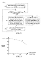
Fig. 2 is a flow diagram illustrating an exemplary power converter operating method for selectively derating a power converter output current during active front end rectifier boost mode operation; -
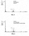
Fig. 3 is a graph illustrating an exemplary output current derating curve as a function of DC voltage boost; -
Fig. 4 illustrates an exemplary lookup table for selectively derating a power converter output current according to DC voltage boost; -
Fig. 5 is a graph illustrating filter inductor current harmonic content for a power converter with an active front end in normal operation with no boost; -
Fig. 6 is a graph illustrating filter inductor current harmonic content for a power converter with boost mode operation of the active front end rectifier with no output current derating; and -
Fig. 7 is a schematic diagram illustrating another embodiment of an active front end power converter driving a DC load with a boosted voltage at a derated output current level according to the present disclosure. - Referring now to the figures, several embodiments or implementations are hereinafter described in conjunction with the drawings, wherein like reference numerals are used to refer to like elements throughout, and wherein the various features are not necessarily drawn to scale. Methods and apparatus are disclosed for operating a motor drive or other active front end power conversion systems with an active front end operative in a boost mode to generate a DC bus with a voltage higher than a peak line to line AC input voltage level. Although illustrated and described below in the context of AC motor drives, the various concepts of the present disclosure find utility in association with other forms of power conversion systems having an active front end converter driving a DC load, wherein the present disclosure is not limited to the illustrated examples.
-
Fig. 1 illustrates an exemplary motor drivepower conversion system 10 receiving single or multiphase AC input power from anexternal power source 2. The illustrated example receives a three phase input, but single phase or other multiphase embodiments are possible. Themotor drive 10 includes aninput filter circuit 20, in this case a three phase LCL filter having grid side inductors L1, L2 and L3 connected to the power leads of thepower source 2 as well as series connected converter side inductors L4, L5 and L6, with filter capacitors C1, C2 and C3 connected between the corresponding grid and converter side inductors and a common connection node, which may but need not be connected to a system ground. Although illustrated in the context of a three phaseLCL filter circuit 20, other alternate circuit configurations can be used, including without limitation LC filters. - The
motor drive 10 includes aninput filter circuit 20, arectifier 30, a DC bus orDC link circuit 40 and anoutput inverter 50, with therectifier 30 and theinverter 50 being operated by acontroller 60. Thecontroller 60 includes arectifier controller 62 with an associatedboost logic circuit 64, aninverter controller 66 and aderating control component 70 operative using one or more lookup tables (LUTs) 72 and/or one or more deratingformulas 74 to selectively derating the rectifier output current when therectifier 30 is operated in boost mode as described further hereinafter. In the illustrated example, thederating control component 70 provides a derated outputcurrent value 76 to theinverter switching controller 66, which in turn provides a DC current command value IDC to therectifier switching controller 62 in order to operate therectifier 30 at a derated output current level. In other possible implementations, thederating components 70 provides a derated outputcurrent value 76 directly to the rectifier switching controller 62 (Fig. 7 below). - The
controller 60 and the components thereof may be implemented as any suitable hardware, processor-executed software, processor-executed firmware, logic, and/or combinations thereof wherein the illustratedcontroller 60 can be implemented largely in processor-executed software or firmware providing various control functions by which thecontroller 60 receives feedback and/or input signals and/or values (e.g., setpoint(s)) and provides rectifier and inverterswitching control signals rectifier 30 and switches S7-S12 of theinverter 50 to convert input power for providing AC output power to drive theload 4. In addition, thecontroller 60 and thecomponents - The
motor drive 10 provides an active front end (AFE) including a switching rectifier (also referred to as a converter) 30 receiving three-phase power from thesource 2 through thefilter circuit 20. Therectifier 30 includes rectifier switches S1-S6, which may be insulated gate bipolar transistors (IGBTs) or other suitable form of semiconductor-based switching devices operable according to a corresponding rectifierswitching control signal 62a to selectively conduct current when actuated. In addition, as seen inFig. 1 , diodes are connected across the individual IGBTs S1-S6. In operation, switching of the rectifier switches S1-S6 is controlled according to pulse width modulated rectifierswitching control signals 62a to provide active rectification of the AC input power from thesource 2 to provide a DC bus voltage Vdc across a DC bus capacitance C4 in aDC link circuit 40. Therectifier 30, moreover, can be selectively operated by the rectifierswitching control component 62 of themotor drive controller 60 for normal operation or boost mode operation according to boostcontrol logic 64. In boost operation, the rectifierswitching control component 62 provides thesignals 62a to cause therectifier 30 to generate the DC bus voltage at a level above the peak line to line AC input voltage received from theinput source 2. - The
drive 10 inFig. 1 further includes aninverter 50 with switches S7-S12 coupled to receive power from theDC bus 40 and to provide AC output power to a motor orother load 4. The inverter switches S7-S12 are operated according to switchingcontrol signals 66a from an inverterswitching control component 66 of thedrive controller 60, and can be any form of suitable high-speed switching devices, including without limitation IGBTs. Theinverter controller 66 also provides a DC current command signal or value IDC to therectifier switching controller 62 to cause therectifier controller 62 to operate the rectifier switches S1-S6 to provide a DC output current to theDC link circuit 40 accordingly. In addition, thecontroller 60 receives various input signals or values, including setpoint signals or values for desired output operation, such as motor speed, position, torque, etc., as well as feedback signals or values representing operational values of various portions of themotor drive 10. Among these are a DC bus voltage feedback signal orvalue 78 representing the DC bus voltage Vdc, and a signal orvalue 79 representing the line to line AC input voltage value. - Referring also to
Figs. 5 and 6 , operation of the activefront end rectifier 30 in boost mode may arise under a variety of circumstances. For instance, amotor drive 10 may be designed for an output current (or horsepower) rating based on receipt of AC input power at a certain nominal voltage level or range, such as 480 V AC in one example. In certain embodiments, thecontroller 60 employs theboost control component 64 to selectively switch the rectifierswitching control component 64 from normal to boost operation, and provides an additional DC bus voltage boost amount required to operate the inverter motor (e.g., a DC bus voltage boost amount) 64a (ΔVdc) to thederating system 70 as well as to therectifier switching controller 62. In certain implementations, moreover, theboost amount 64a may be preprogrammed into thecontroller 60, or may be user configurable. For example, themotor drive 10 may be designed for a certain AC input voltage value or range (e.g., 480 V, 60 Hz), but may be installed for use in an environment providing only 380 V AC input. In such a situation, thecontroller 60 may be programmed with a fixed DCvoltage boost value 64a for use by therectifier switching controller 62 and thederating system 70. - As seen in
Fig. 5 , normal operation of the rectifier 30 (without boosting) with a nominal AC input voltage results in certain harmonic content in thefilter circuit 20.Fig. 5 shows agraph 300 illustrating the harmonic content as a percentage of rated peak current for an exemplary motor drive operated with a 400 V AC input providing a 560 V DC bus without use of boost operation, and with an output from theinverter 50 providing a 380 V AC output to a load. Under this condition, the regular DC bus voltage to operate a 400 V motor will be 560 V DC. In this non-boosting rectifier operational condition, a certain level of harmonics are seen at 302, approximately near 4 kHz for a 60 Hz AC input frequency. However, if the system is to drive a 460 V motor, the DC bus voltage needs to be increased to 680 V DC. As a result, the additional DC voltage boost amount is 680 - 560 = 120 V DC. Agraph 310 inFig. 6 shows percent rated peak current frequency content for thesame converter 10 operated again from a 400 V AC input source, with active front end rectifier boost operation being used to boost the DC voltage Vdc above the line to line input voltage peak, in this case to 680 V DC. In this case, moreover, theoutput inverter 50 provides a 460 V AC output with no derating of the rectifier output current. As seen inFig. 6 , the corresponding peak currentharmonic content 312 is significantly higher than the correspondingharmonic content 302 in the non-boosting example ofFig. 5 . - The inventors have appreciated that increased harmonic content in boost mode leads to increased operating temperature of the inductor cores of the filter circuit inductors L4-L6. In particular, the converter side inductors L4-L6 may suffer thermal stress caused by boost operation of the active
front end rectifier 30. In this regard, motor drives and other active front endpower conversion systems 10 are typically designed around a nominal rating condition, including rated AC input voltage levels and corresponding DC bus voltages and currents, as well as drive output power or current levels. In order to economize a design with respect to cost, heat and cabinet space, the input filter inductors L are typically designed around the nominal rating condition, and thus switching operation to boost mode may cause excessive thermal stress to the inductors as the increased harmonics heat up the core structure. As noted above, thermal shutoff switches can be used to attempt to detect overheating of inductor cores, but extensive sensor coverage is both expensive and adds to the complexity of themotor drive system 10. Moreover, many situations arise in practice in which it is desirable to operate apower converter 10 with the rectifier boosting the DC bus voltage beyond the peak line AC input voltage value. Simply providing thermal shutdown capability may protect the filter inductors L from thermal stress, but may generate undesirable system shutdowns. Another approach to address this issue is to design the filter inductors L to accommodate the higher harmonic content associated with boost mode operation, but this requires increasing the size and cost of theinput filter circuit 20 and the components thereof. - The present disclosure addresses these shortcomings of the prior art by selectively derating the motor drive output, in particular the maximum output current from the
rectifier 30, based on boost mode operation. Using this novel technique, the filter inductors L need not be oversized, and the system can operate intermittently or even continuously in rectifier boost mode without triggering undesirable shutdowns, while protecting the filter inductors L from thermal stress. In particular, thecontroller 60 employs thederating system 70 which provides theinverter switching controller 66 with a derated outputcurrent value 76 during active front end boost mode operation. Theinverter controller 66 in this embodiment provides a lowered or derated DC current command value IDC to therectifier controller 62 in order to operate therectifier 30 according to the derated outputcurrent value 76 during active front end boost mode. Thederating amount 76 is determined according to the AC input voltage present at the source 2 (or the AC input voltage level at other measure points in the LCL filter circuit 20) based on one or more feedback signals orvalues 79, and also according to the DC bus voltage (feedback signal or value 78) and an amount of additional DCbus voltage boost 64a (ΔVdc) obtained from theboost control component 64. In certain embodiments, the derated outputcurrent value 76 can be represented as a percentage of the nominal output current rating for either theinverter 50 or therectifier 30. In practice, moreover, the derated outputcurrent value 76 is less than or equal to the maximum output current rating for thepower conversion system 10. In the embodiment ofFig. 7 below, the derated outputcurrent value 76 is provided directly to therectifier switching controller 62, and may be representative of a percentage of the nominal DC output current rating for therectifier 30. - Referring also to
Fig. 2 , amethod 100 is illustrated for operating a power conversion system, which may be employed in themotor drive 10 ofFig. 1 or the activefront end converter 10 ofFig. 7 below, or in any other power conversion system. While themethod 100 is illustrated and described below in the form of a series of acts or events, it will be appreciated that the various methods of the disclosure are not limited by the illustrated ordering of such acts or events. In this regard, except as specifically provided hereinafter, some acts or events may occur in different order and/or concurrently with other acts or events apart from those illustrated and described herein in accordance with the disclosure. It is further noted that not all illustrated steps may be required to implement a process or method in accordance with the present disclosure, and one or more such acts may be combined. The illustratedmethod 100 other methods of the disclosure may be implemented in hardware, processor-executed software, or combinations thereof, such as in theexemplary controller 60 described herein, and may be embodied in the form of computer executable instructions stored in a tangible, non-transitory computer readable medium, such as in a memory operatively associated with thecontroller 60 in one example. - The
drive 10 or therectifier 30 thereof may be operated with a normal 100% output current rating as shown at 102 inFig. 2 . A determination is made at 104 as to whether therectifier 30 is operating in boost mode. If not (NO at 104), thedrive 10 continues to be operated at the normal output current rating at 102. If the rectifier is in boost mode (YES at 104), thecontroller 60 determines a derated output current value (76 inFig. 1 above) according to the line to line AC input voltage value (e.g., from feedback signal or value 79) and according to the DC busvoltage boost amount 64a from theboost control component 64, denoted in the figure as ΔVdc. In certain embodiments, the voltage boost amount is expressed in terms of volts DC, although not a strict requirement. For instance, if the nominal DC voltage (e.g., approximately the peak line to line AC input voltage value) is 560 V DC, boost mode operation to provide a DC bus voltage of 680 V DC would represent a 120 V DC bus voltage boost amount (ΔVdc = 120 V DC). Other suitable representation schemes can be employed by which a DC bus voltage boost amount is used which in some way represents the effect of boost mode operation on the DC bus voltage Vdc. - The determination of the derated output
current value 76 can be performed in a variety of ways. In one possible embodiment, themethod 100 ofFig. 2 provides for use of a lookup table (e.g., lookup table 72 inFig. 1 ), with the derated outputcurrent value 76 being obtained from a lookup table 72 corresponding to the line to line AC input voltage value. This can be accomplished, for instance, as seen at 106 inFig. 2 , by indexing the lookup table 72 which corresponds to the AC input voltage level in order to determine the drive outputcurrent derating value 76 associated with the DCvoltage boost amount 64a ΔVdc. In another possible embodiment (shown in dashed line inFig. 2 ) a derating formula may be solved at 107 corresponding to the AC input voltage level to determine the drive or rectifier outputcurrent derating value 76 according to the DC voltageboost amount ΔVdc 64a. Thedrive output inverter 50 is then operated at 108 according to the derated outputcurrent value 76, and provides the DC current command value to therectifier switching controller 62 to operate therectifier 30 according to thederating value 76. For example, themotor drive 10 and theinverter 50 thereof may receive one or more setpoint values representing a desired load drive condition, such as a setpoint torque, speed, position, etc. Theinverter controller 66 in certain embodiments uses the outputcurrent derating value 76 as a maximum limit on the output current provided to themotor load 4. Thus, theinverter 50 will provide outputs, including the desired DC current command value IDC such that thederating value 76 is not exceeded, thereby ensuring that the filter inductors L are not thermally stressed. Theprocess 100 then returns to again determine at 104 whether the rectifier continues to be operated in the boost mode as described above, and the process continues in this fashion as described above. - Referring also to
Figs. 3 and4 ,Fig. 3 shows agraph 200 depicting acurve 76 of percent rated current versus DC voltage boost amount for a 400 V AC line to line input voltage level, andFig. 4 illustrates an exemplary lookup table 72 corresponding to the curve 202 inFig. 3 . The table inFig. 4 in this example is chosen from a plurality of such tables 72, with each table 72 being associated with a particular AC input voltage value. As seen inFig. 3 , when the DC bus voltage is 114 V above normal, the drive or rectifier current rating is 100% (e.g., the derated outputcurrent value 76 is equal to the maximum output current rating for thepower converter 10 as a whole or therectifier 30 thereof). In this case, thecurve 76 represents maximum steady state load conditions for which the filter inductors L will not be thermally stressed, and thus boosting the DC bus voltage by 114 V will allow the filter inductors L to avoid overheating. However, as the DC busvoltage boost amount 64a increases to 160 V and 184 V, the derated outputcurrent value 76 drops to approximately 93% and 85%, respectively. At these levels, therefor, controlling theinverter 50 , and hence therectifier 30, to provide no more than this derated amount of output current allows the filter inductors L to continue operation within the proper thermal range. In certain embodiments, a formula 74 (Fig. 1 ) can be used to evaluate thederating curve 76 for any given DC bus voltage boost amount, for example, a polynomial function. - Moreover, the
curve 76 inFig. 3 and a corresponding lookup table 72 inFig. 4 correspond to a particular line to line AC input voltage value, where one or more suchparametric functions 74 and/or lookup tables 72 may be provided. Thus, for instance, thederating system 70 inFig. 1 may be configured to select an appropriate (e.g., closest)function 74 or lookup table 72 based on the line to line AC input voltage present in the system 10 (e.g., according to the input voltage feedback signal or value 79), and to use that function or lookup table to determine the derated outputcurrent value 76 according to the AC input line voltage value and according to the DC busvoltage boost amount 64a. Moreover, as seen inFig. 4 , certain embodiments may employ different lookup tables 72 for various AC input voltage levels, such as 380 V, 390 V, 400 V, etc. Likewise, thederating system 70 may employ one of a plurality ofderating formulas 74, each corresponding to a different AC input voltage level, with thederating system 70 selecting a closest or mostappropriate formula 74 according to thefeedback 79. In one possible embodiment, thederating system 70 of thecontroller 60 is configured to dynamically receive the input voltage feedback signal orvalue 79 and choose the closest lookup table 72 for use in determining the derated outputcurrent value 76. Similarly, thederating system 70 may select from among a plurality ofderating formulas 74 based on theAC input value 79. - When using a selected lookup table 72, moreover, the
derating system 70 of thecontroller 60 may utilize interpolation for the derated output current value determination. As seen inFig. 4 , for instance, thecontroller 60 may interpolate between derated outputcurrent values 76 of the lookup table 72 corresponding to DC bus voltage boost amounts 64a above and below the DC bus voltage boost amount present in thepower system 10 to derive the derated outputcurrent value 76 for use in operating theinverter 50, and hence therectifier 30. For example, if the DC busvoltage boost amount 64a in the example ofFig. 4 was 175 V DC (ΔVdc = 175), thecontroller 60 could use any suitable interpolation technique (e.g., linear or otherwise) with the corresponding derated output current values (e.g., 91% and 87%) corresponding to the DC bus voltage boost amounts (e.g., 170 V DC and 180 V DC) above and below the actual voltage boost in order to derive or compute thevalue 76 through interpolation (e.g., 89% in this example). - In certain implementations, the values of the lookup table 72 and the parameters of the
derating formulas 74 can be selected such that they correspond to maximum steady state load operating conditions of thepower converter 10 for which the input filter inductor (e.g., L) is designed not to overheat. This correlation can be obtained by any suitable means, such as by empirical testing to derive output current derating values 76 for a number of different DC busvoltage boost value 64a at which the temperature of the inductor core is at the rated value (or within an acceptable range thereof), and constructing a corresponding table 72 for each of a number of AC input voltage values. Likewise, experimental data can be used to derive formulas 74 (e.g., linear, polynomial, etc.) based on curve fitting or other suitable mathematical technique. -
Fig. 7 illustrates another exemplary power conversion system, in this case an activefront end converter 10 with a switchingrectifier 30 and correspondingrectifier switching controller 62 as described above. In this example, however, therectifier 30 provides a DC output to drive anexternal DC load 50. In this case, an active front endoutput derating component 70 provides the derated outputcurrent value 76 to therectifier switching controller 62 directly. In operation, therectifier controller 62 provides the switchingcontrol signals 62a in boost mode to provide boosted or increased DC output voltage to theload 50 above the peak line to line AC input voltage value, and also controls the DC output load current ILOAD provided to theload 50 so as not to exceed the derated outputcurrent value 76. As seen inFig. 7 , therefore, the concepts of the present disclosure advantageously facilitate AFE boost mode operation with derated rectifier output current limiting in a variety of applications for any number of types ofDC load 50, such as capacitor bank charging, fuel cells, solar cells, etc., in addition to the above-described motor drive applications in which therectifier 30 provides a boosted DC voltage across aDC bus circuit 40 for use by an inverter load. - In accordance with further aspects of the present disclosure, a non-transitory computer readable medium is provided, such as a computer memory, a memory within a power converter control system (e.g., controller 100), a CD-ROM, floppy disk, flash drive, database, server, computer, etc.), which includes computer executable instructions for performing the above-described methods. The above examples are merely illustrative of several possible embodiments of various aspects of the present disclosure, wherein equivalent alterations and/or modifications will occur to others skilled in the art upon reading and understanding this specification and the annexed drawings. In particular regard to the various functions performed by the above described components (assemblies, devices, systems, circuits, and the like), the terms (including a reference to a "means") used to describe such components are intended to correspond, unless otherwise indicated, to any component, such as hardware, processor-executed software, or combinations thereof, which performs the specified function of the described component (i.e., that is functionally equivalent), even though not structurally equivalent to the disclosed structure which performs the function in the illustrated implementations of the disclosure. In addition, although a particular feature of the disclosure may have been disclosed with respect to only one of several implementations, such feature may be combined with one or more other features of the other implementations as may be desired and advantageous for any given or particular application. Also, to the extent that the terms "including", "includes", "having", "has", "with", or variants thereof are used in the detailed description and/or in the claims, such terms are intended to be inclusive in a manner similar to the term "comprising".
-
-
Embodiment 1. A method for operating a power conversion system, the method comprising:- operating a rectifier of the power conversion system in a boost mode to provide a DC bus voltage higher than a peak line to line AC input voltage value;
- determining a derated output current value according to the line to line AC input voltage value and according to a DC bus voltage boost amount, the derated output current value being less than or equal to a maximum output current rating for the rectifier; and
- operating the rectifier according to the derated output current value.
-
Embodiment 2. The method ofembodiment 1, wherein determining the derated output current value comprises:- obtaining the derated output current value corresponding to the DC bus voltage boost amount from a lookup table corresponding to the line to line AC input voltage value.
-
Embodiment 3. The method ofembodiment 1, wherein determining the derated output current value comprises:- selectively interpolating two derated output current values of the lookup table corresponding to DC bus voltage boost amounts above and below the DC bus voltage boost amount present in the power conversion system to derive the derated output current value.
-
Embodiment 4. The method ofembodiment 2, wherein determining the derated output current value comprises:- selecting a given one of a plurality of lookup tables corresponding to the line to line AC input voltage value; and
- obtaining the derated output current value corresponding to the DC bus voltage boost amount from the given one of the plurality of lookup tables.
-
Embodiment 5. The method ofembodiment 4, wherein determining the derated output current value comprises:- selectively interpolating two derated output current values of the given one of the plurality of lookup tables corresponding to DC bus voltage boost amounts above and below the DC bus voltage boost amount present in the power conversion system to derive the derated output current value.
-
Embodiment 6. The method ofembodiment 2, wherein the DC bus voltage boost amounts and corresponding derated output current values of the lookup table correspond to maximum steady state load operating conditions of the power conversion system for which an input filter inductor is designed not to overheat. -
Embodiment 7. The method ofembodiment 1, wherein determining the derated output current value comprises:- solving at least one derating formula according to the DC bus voltage boost amount.
-
Embodiment 8. The method ofembodiment 7, wherein determining the derated output current value comprises:- selecting a given one of a plurality of derating formulas corresponding to the line to line AC input voltage value; and
- solving the given one of the plurality of the rating formulas according to the DC bus voltage boost amount.
-
Embodiment 9. A non-transitory computer readable medium with computer executable instructions for operating a power conversion system, the computer readable medium comprising computer executable instructions for:- operating a rectifier of the power conversion system in a boost mode to provide a DC bus voltage higher than a peak line to line AC input voltage value;
- determining a derated output current value according to the line to line AC input voltage value and according to a DC bus voltage boost amount, the derated output current value being less than or equal to a maximum output current rating for the rectifier; and
- operating the rectifier according to the derated output current value.
-
Embodiment 10. The computer readable medium ofembodiment 9, wherein the computer executable instructions for determining the derated output current value comprise computer executable instructions for:- obtaining the derated output current value corresponding to the DC bus voltage boost amount from a lookup table corresponding to the line to line AC input voltage value.
- Embodiment 11. The computer readable medium of
embodiment 10, wherein the computer executable instructions for determining the derated output current value comprise computer executable instructions for:- selectively interpolating two derated output current values of the lookup table corresponding to DC bus voltage boost amounts above and below the DC bus voltage boost amount present in the power conversion system to derive the derated output current value.
- Embodiment 12. The computer readable medium of
embodiment 10, comprising at least one lookup table including a plurality of derated output current values and corresponding DC bus voltage boost amounts. - Embodiment 13. The computer readable medium of
embodiment 10, wherein the computer executable instructions for determining the derated output current value comprise computer executable instructions for:- solving at least one derating formula according to the DC bus voltage boost amount.
- Embodiment 14. A power conversion system, comprising:
- a filter circuit comprising at least one inductor;
- an active rectifier comprising a plurality of rectifier switching devices coupled to receive AC input power from an external power source through the filter circuit and to provide a DC bus voltage at a DC bus; and
- a controller providing rectifier control signals to the rectifier switching devices to selectively operate the rectifier in a boost mode to provide the DC bus voltage higher than a peak line to line AC input voltage value, the controller being operative to determine a derated output current value according to the line to line AC input voltage value and according to a DC bus voltage boost amount, and to selectively operate the rectifier according to the derated output current value.
- Embodiment 15. The power conversion system of embodiment 14, wherein the controller is operative to obtain the derated output current value corresponding to the DC bus voltage boost amount from a lookup table corresponding to the line to line AC input voltage value.
- Embodiment 16. The power conversion system of embodiment 15, wherein the controller is operative to selectively interpolate two derated output current values of the lookup table corresponding to DC bus voltage boost amounts above and below the DC bus voltage boost amount present in the power conversion system to derive the derated output current value.
- Embodiment 17. The power conversion system of embodiment 15, wherein the controller is operative to select a given one of a plurality of lookup tables corresponding to the line to line AC input voltage value, and to obtain the derated output current value corresponding to the DC bus voltage boost amount from the given one of the plurality of lookup tables.
- Embodiment 18. The power conversion system of embodiment 17, wherein the controller is operative to selectively interpolate two derated output current values of the given one of the plurality of lookup tables corresponding to DC bus voltage boost amounts above and below the DC bus voltage boost amount present in the power conversion system to derive the derated output current value.
- Embodiment 19. The power conversion system of embodiment 14, wherein the controller is operative to determine the derated output current value by solving at least one derating formula according to the DC bus voltage boost amount.
-
Embodiment 20. The power conversion system of embodiment 14, wherein the derated output current value and the corresponding DC bus voltage boost amount correspond to a maximum steady state load operating condition of the power conversion system for which the at least one inductor is designed not to overheat. -
external power source 2 power conversion system 10 filter circuit 20 rectifier 30 DC bus 40 controller 60 lookup table 72 derating value 74 output current value 76
Claims (10)
- A method (100) for operating a power conversion system (10), the method comprising:operating a rectifier (30) of the power conversion system (10) in a boost mode to provide an additional boost to generate a DC bus voltage (Vdc) higher than a peak line to line AC input voltage value;determining a derated output current value (76) according to the line to line AC input voltage value and according to a DC bus voltage boost amount (ΔVdc), the derated output current value (76) being less than or equal to a maximum output current rating for the rectifier (30); andoperating the rectifier (30) according to the derated output current value.
- The method (100) of claim 1, wherein determining the derated output current value (76) comprises:obtaining the derated output current value (76) corresponding to the DC bus voltage boost amount (ΔVdc) from a lookup table (72) corresponding to the line to line AC input voltage value.
- The method (100) of claim 1, wherein determining the derated output current value (76) comprises:selectively interpolating two derated output current values of the lookup table (72) corresponding to DC bus voltage boost amounts (ΔVdc) above and below the DC bus voltage boost amount present in the power conversion system (10) to derive the derated output current value (76).
- The method (100) of claim 2, wherein the DC bus voltage boost amounts (ΔVdc) and corresponding derated output current values (76) of the lookup table (72) correspond to maximum steady state load operating conditions of the power conversion system (10) for which an input filter inductor (L1-L6) is designed not to overheat.
- The method (100) of claim 1, wherein determining the derated output current value (76) comprises:solving at least one derating formula (74) according to the DC bus voltage boost amount (ΔVdc).
- A non-transitory computer readable medium with computer executable instructions for operating a power conversion system (10), the computer readable medium comprising computer executable instructions for:operating a rectifier (30) of the power conversion system (10) in a boost mode to provide a DC bus voltage (Vdc) higher than a peak line to line AC input voltage value;determining a derated output current value (76) according to the line to line AC input voltage value and according to a DC bus voltage boost amount (ΔVdc), the derated output current value (76) being less than or equal to a maximum output current rating for the rectifier (30); andoperating the rectifier (30) according to the derated output current value.
- A power conversion system (10), comprising:a filter circuit (20) comprising at least one inductor (L);an active rectifier (30) comprising a plurality of rectifier switching devices (S1-S6) coupled to receive AC input power from an external power source (2) through the filter circuit (20) and to provide a DC bus voltage (Vdc) at a DC bus (40);a controller (60) providing rectifier control signals (62a) to the rectifier switching devices (S1-S6) to selectively operate the rectifier (30) in a boost mode to provide the DC bus voltage (Vdc) higher than a peak line to line AC input voltage value, the controller (60) being operative to determine a derated output current value (76) according to the line to line AC input voltage value and according to a DC bus voltage boost amount (ΔVdc), and to selectively operate the rectifier (30) according to the derated output current value (76).
- The power conversion system (10) of claim 7, wherein the controller (60) is operative to obtain the derated output current value (76) corresponding to the DC bus voltage boost amount (ΔVdc) from a lookup table (72) corresponding to the line to line AC input voltage value.
- The power conversion system (10) of claim 7, wherein the controller (60) is operative to determine the derated output current value (76) by solving at least one derating formula (74) according to the DC bus voltage boost amount (ΔVdc).
- The power conversion system (10) of claim 7, wherein the derated output current value (76) and the corresponding DC bus voltage boost amount (ΔVdc) correspond to a maximum steady state load operating condition of the power conversion system (10) for which the at least one inductor (L) is designed not to overheat.
Applications Claiming Priority (1)
| Application Number | Priority Date | Filing Date | Title |
|---|---|---|---|
| US13/832,214 US9461559B2 (en) | 2013-03-15 | 2013-03-15 | Active front end power converter with boost mode derating to protect filter inductor |
Publications (2)
| Publication Number | Publication Date |
|---|---|
| EP2779391A1 true EP2779391A1 (en) | 2014-09-17 |
| EP2779391B1 EP2779391B1 (en) | 2019-01-16 |
Family
ID=50280261
Family Applications (1)
| Application Number | Title | Priority Date | Filing Date |
|---|---|---|---|
| EP14160229.2A Active EP2779391B1 (en) | 2013-03-15 | 2014-03-17 | Active front end power converter with boost mode derating to protect filter inductor |
Country Status (4)
| Country | Link |
|---|---|
| US (2) | US9461559B2 (en) |
| EP (1) | EP2779391B1 (en) |
| CN (1) | CN104052306B (en) |
| BR (1) | BR102014006330B1 (en) |
Cited By (3)
| Publication number | Priority date | Publication date | Assignee | Title |
|---|---|---|---|---|
| CN112019027A (en) * | 2019-05-31 | 2020-12-01 | 广东美的制冷设备有限公司 | Drive control method, device, household appliance and computer readable storage medium |
| CN112019028A (en) * | 2019-05-31 | 2020-12-01 | 广东美的制冷设备有限公司 | Drive control method, device, household appliance and computer readable storage medium |
| EP3731391A4 (en) * | 2017-12-20 | 2021-02-24 | Power Electronics España, S.L. | System and method for dynamic over-current protection for power converters |
Families Citing this family (23)
| Publication number | Priority date | Publication date | Assignee | Title |
|---|---|---|---|---|
| US9819255B2 (en) | 2014-07-08 | 2017-11-14 | Rockwell Automation Technologies, Inc. | LCL filter resonance mitigation technique for voltage source converters |
| JP5946880B2 (en) * | 2014-09-26 | 2016-07-06 | ファナック株式会社 | Motor control device having LCL filter protection function |
| US9800134B2 (en) | 2015-02-25 | 2017-10-24 | Rockwell Automation Technologies, Inc. | Motor drive with LCL filter inductor with built-in passive damping resistor for AFE rectifier |
| KR101980995B1 (en) * | 2015-04-13 | 2019-05-21 | 도시바 캐리어 가부시키가이샤 | Motor drive device |
| US10511169B2 (en) * | 2016-02-20 | 2019-12-17 | Electronic Power Design, Inc. | System and method for a dynamic switchable active front end—dynamic switchable active harmonic filtering system |
| US10263558B2 (en) * | 2016-03-16 | 2019-04-16 | Rockwell Automation Technologies, Inc. | Phase loss detection in active front end converters |
| US9923469B2 (en) | 2016-05-09 | 2018-03-20 | Rockwell Automation Technologies, Inc. | Motor drive filter damping |
| US9837924B1 (en) | 2016-06-02 | 2017-12-05 | Rockwell Automation Technologies, Inc. | Precharge apparatus for power conversion system |
| US10281503B2 (en) * | 2016-11-11 | 2019-05-07 | Fluke Corporation | Non-contact voltage measurement system using multiple capacitors |
| US10352967B2 (en) | 2016-11-11 | 2019-07-16 | Fluke Corporation | Non-contact electrical parameter measurement systems |
| CN108071600B (en) | 2016-11-17 | 2019-11-05 | 台达电子工业股份有限公司 | Electronically commutated fan system |
| US10797589B2 (en) * | 2017-09-28 | 2020-10-06 | Texas Instruments Incorporated | Methods and apparatus to compensate for power factor loss using a phasor cancellation based compensation scheme |
| US11482942B2 (en) * | 2017-10-31 | 2022-10-25 | Otis Elevator Company | Single phase operation of three phase regenerative drives |
| US10158299B1 (en) * | 2018-04-18 | 2018-12-18 | Rockwell Automation Technologies, Inc. | Common voltage reduction for active front end drives |
| US10811990B1 (en) * | 2019-03-29 | 2020-10-20 | Rockwell Automation Technologies, Inc. | Multi-segment and nonlinear droop control for parallel operating active front end power converters |
| CN112019016B (en) * | 2019-05-31 | 2021-09-24 | 广东美的制冷设备有限公司 | Operation control method, device, circuit, home appliance and computer storage medium |
| US10784797B1 (en) * | 2019-06-19 | 2020-09-22 | Rockwell Automation Technologies, Inc. | Bootstrap charging by PWM control |
| US11211879B2 (en) | 2019-09-23 | 2021-12-28 | Rockwell Automation Technologies, Inc. | Capacitor size reduction and lifetime extension for cascaded H-bridge drives |
| US20230238876A1 (en) * | 2020-04-28 | 2023-07-27 | Prodrive Technologies Innovation Services B.V. | Electrical power converter |
| CN111800029B (en) * | 2020-08-07 | 2024-01-23 | 江苏吉泰科电气有限责任公司 | Low-power consumption control method for battery simulator |
| EP4222852A1 (en) * | 2020-10-01 | 2023-08-09 | Vestas Wind Systems A/S | Method for reduction of dc link busbar and capacitor current, by adjustment of a pwm carrier delay |
| US12057732B2 (en) * | 2022-09-12 | 2024-08-06 | Rivian Ip Holdings, Llc | High voltage discharge |
| US20250132686A1 (en) * | 2023-10-20 | 2025-04-24 | Infineon Technologies Austria Ag | Multi-Phase Resonant Power Converter |
Citations (2)
| Publication number | Priority date | Publication date | Assignee | Title |
|---|---|---|---|---|
| US20050068001A1 (en) * | 2001-11-23 | 2005-03-31 | Danfoss Drives A/S | Frequency converter for different mains voltages |
| US20120235607A1 (en) * | 2009-11-04 | 2012-09-20 | Rockwell Automation Technologies, Inc. | Dc bus boost method and system for regenerative brake |
Family Cites Families (15)
| Publication number | Priority date | Publication date | Assignee | Title |
|---|---|---|---|---|
| US6346778B1 (en) * | 1998-01-20 | 2002-02-12 | Bytecraft Pty Ltd | AC power converter |
| US6963178B1 (en) * | 1998-12-07 | 2005-11-08 | Systel Development And Industries Ltd. | Apparatus for controlling operation of gas discharge devices |
| US7164254B2 (en) | 2005-02-28 | 2007-01-16 | Rockwell Automation Technologies, Inc. | Modulation methods and apparatus for reducing common mode voltages |
| US7106025B1 (en) | 2005-02-28 | 2006-09-12 | Rockwell Automation Technologies, Inc. | Cancellation of dead time effects for reducing common mode voltages |
| US7332885B2 (en) * | 2005-09-02 | 2008-02-19 | Johnson Controls Technology Company | Ride-through method and system for HVAC&R chillers |
| JP5259077B2 (en) * | 2006-12-04 | 2013-08-07 | 株式会社京三製作所 | Instantaneous voltage drop compensation circuit, power converter, instantaneous voltage drop compensation method, and instantaneous voltage drop compensation program |
| US7495410B2 (en) | 2007-01-30 | 2009-02-24 | Rockwell Automation Technologies, Inc. | Systems and methods for improved motor drive power factor control |
| US7683568B2 (en) | 2007-09-28 | 2010-03-23 | Rockwell Automation Technologies, Inc. | Motor drive using flux adjustment to control power factor |
| US8174853B2 (en) * | 2007-10-30 | 2012-05-08 | Johnson Controls Technology Company | Variable speed drive |
| US8035536B2 (en) * | 2007-11-08 | 2011-10-11 | Delta Electronics, Inc. | Digitally controlled three-phase PFC rectifier |
| US8334616B2 (en) * | 2008-09-19 | 2012-12-18 | Electric Power Research Institute, Inc. | Photovoltaic integrated variable frequency drive |
| US7990097B2 (en) | 2008-09-29 | 2011-08-02 | Rockwell Automation Technologies, Inc. | Power conversion system and method for active damping of common mode resonance |
| US7830036B2 (en) | 2008-09-30 | 2010-11-09 | Rockwell Automation Technologies, Inc. | Power electronic module pre-charge system and method |
| US8503207B2 (en) | 2010-09-29 | 2013-08-06 | Rockwell Automation Technologies, Inc. | Discontinuous pulse width drive modulation method and apparatus for reduction of common-mode voltage in power conversion systems |
| US20130249431A1 (en) * | 2012-03-05 | 2013-09-26 | Luxera, Inc. | Dimmable Hybrid Adapter for a Solid State Lighting System, Apparatus and Method |
-
2013
- 2013-03-15 US US13/832,214 patent/US9461559B2/en active Active
-
2014
- 2014-03-17 EP EP14160229.2A patent/EP2779391B1/en active Active
- 2014-03-17 CN CN201410098926.9A patent/CN104052306B/en not_active Expired - Fee Related
- 2014-03-17 BR BR102014006330-7A patent/BR102014006330B1/en not_active IP Right Cessation
-
2016
- 2016-10-03 US US15/283,507 patent/US9973137B2/en active Active
Patent Citations (2)
| Publication number | Priority date | Publication date | Assignee | Title |
|---|---|---|---|---|
| US20050068001A1 (en) * | 2001-11-23 | 2005-03-31 | Danfoss Drives A/S | Frequency converter for different mains voltages |
| US20120235607A1 (en) * | 2009-11-04 | 2012-09-20 | Rockwell Automation Technologies, Inc. | Dc bus boost method and system for regenerative brake |
Non-Patent Citations (2)
| Title |
|---|
| ANNABELLE VAN ZYL ET AL: "Voltage Sag Ride-Through for Adjustable-Speed Drives With Active Rectifiers", IEEE TRANSACTIONS ON INDUSTRY APPLICATIONS, IEEE SERVICE CENTER, PISCATAWAY, NJ, US, vol. 34, no. 6, 1 December 1998 (1998-12-01), XP011022496, ISSN: 0093-9994 * |
| STOCKMAN K ET AL: "Embedded solutions to protect textile processes against voltage sags", CONFERENCE RECORD OF THE 2002 IEEE INDUSTRY APPLICATIONS CONFERENCE : 37TH IAS ANNUAL MEETING ; 13 - 18 OCTOBER 2002, PITTSBURGH, PENNSYLVANIA, USA; [CONFERENCE RECORD OF THE IEEE INDUSTRY APPLICATIONS CONFERENCE. IAS ANNUAL MEETING], IEEE SERVICE CE, 13 October 2002 (2002-10-13), pages 2561, XP032143166, ISBN: 978-0-7803-7420-1, DOI: 10.1109/IAS.2002.1042807 * |
Cited By (4)
| Publication number | Priority date | Publication date | Assignee | Title |
|---|---|---|---|---|
| EP3731391A4 (en) * | 2017-12-20 | 2021-02-24 | Power Electronics España, S.L. | System and method for dynamic over-current protection for power converters |
| US11283346B2 (en) | 2017-12-20 | 2022-03-22 | Power Electronics España, S.L. | System and method for dynamic over-current protection for power converters |
| CN112019027A (en) * | 2019-05-31 | 2020-12-01 | 广东美的制冷设备有限公司 | Drive control method, device, household appliance and computer readable storage medium |
| CN112019028A (en) * | 2019-05-31 | 2020-12-01 | 广东美的制冷设备有限公司 | Drive control method, device, household appliance and computer readable storage medium |
Also Published As
| Publication number | Publication date |
|---|---|
| CN104052306B (en) | 2017-06-23 |
| US9461559B2 (en) | 2016-10-04 |
| CN104052306A (en) | 2014-09-17 |
| US20140268953A1 (en) | 2014-09-18 |
| EP2779391B1 (en) | 2019-01-16 |
| BR102014006330B1 (en) | 2021-04-20 |
| US20170025981A1 (en) | 2017-01-26 |
| BR102014006330A2 (en) | 2016-07-12 |
| US9973137B2 (en) | 2018-05-15 |
Similar Documents
| Publication | Publication Date | Title |
|---|---|---|
| US9973137B2 (en) | Active front end power converter with boost mode derating to protect filter inductor | |
| EP2779405B1 (en) | Methods and apparatus for continuous and discontinuous active rectifier boost operation to increase power converter rating | |
| EP3657661B1 (en) | Conversion circuit, control method, and power supply device | |
| US8816625B2 (en) | Integrated regenerative AC drive with solid state precharging | |
| US9825518B2 (en) | System and method for over-current protection | |
| Teichmann et al. | A comparison of three-level converters versus two-level converters for low-voltage drives, traction, and utility applications | |
| US8570773B2 (en) | Power converter system and method | |
| WO2014167714A1 (en) | Power conversion device, motor drive device provided therewith, fan provided with said motor drive device, compressor, and air conditioner, refrigerator, and freezer provided with said fan and compressor | |
| US9214875B2 (en) | Multilevel inverter | |
| US11050360B2 (en) | Power conversion device | |
| JP3780949B2 (en) | Power converter | |
| Shin et al. | Active DC-link circuit for single-phase diode rectifier system with small capacitance | |
| EP3100346B1 (en) | Unidirectional matrix converter with regeneration system | |
| JP2006288161A (en) | Power converter | |
| JP6228057B2 (en) | Power control apparatus and power control method | |
| JPH1028378A (en) | Power conversion device control method and power conversion system control method | |
| JP6513564B2 (en) | Inverter device capable of resonance avoidance | |
| JP5348484B2 (en) | Load drive system | |
| JP6237400B2 (en) | Power generation device, control device, control method, power generation system, power conversion device and system | |
| JPWO2020246038A1 (en) | Motor drive, blower, compressor and air conditioner | |
| Zargari et al. | A medium voltage AC drive with integrated isolation transformer and active front end |
Legal Events
| Date | Code | Title | Description |
|---|---|---|---|
| 17P | Request for examination filed |
Effective date: 20140317 |
|
| AK | Designated contracting states |
Kind code of ref document: A1 Designated state(s): AL AT BE BG CH CY CZ DE DK EE ES FI FR GB GR HR HU IE IS IT LI LT LU LV MC MK MT NL NO PL PT RO RS SE SI SK SM TR |
|
| AX | Request for extension of the european patent |
Extension state: BA ME |
|
| PUAI | Public reference made under article 153(3) epc to a published international application that has entered the european phase |
Free format text: ORIGINAL CODE: 0009012 |
|
| R17P | Request for examination filed (corrected) |
Effective date: 20150306 |
|
| RBV | Designated contracting states (corrected) |
Designated state(s): AL AT BE BG CH CY CZ DE DK EE ES FI FR GB GR HR HU IE IS IT LI LT LU LV MC MK MT NL NO PL PT RO RS SE SI SK SM TR |
|
| REG | Reference to a national code |
Ref country code: DE Ref legal event code: R079 Ref document number: 602014039893 Country of ref document: DE Free format text: PREVIOUS MAIN CLASS: H02M0001320000 Ipc: H02M0007217000 |
|
| GRAP | Despatch of communication of intention to grant a patent |
Free format text: ORIGINAL CODE: EPIDOSNIGR1 |
|
| STAA | Information on the status of an ep patent application or granted ep patent |
Free format text: STATUS: GRANT OF PATENT IS INTENDED |
|
| RIC1 | Information provided on ipc code assigned before grant |
Ipc: H02M 1/42 20070101ALI20180809BHEP Ipc: H02M 7/217 20060101AFI20180809BHEP Ipc: H02M 1/00 20060101ALI20180809BHEP Ipc: H02M 1/32 20070101ALI20180809BHEP Ipc: H02M 7/219 20060101ALI20180809BHEP |
|
| INTG | Intention to grant announced |
Effective date: 20180912 |
|
| GRAS | Grant fee paid |
Free format text: ORIGINAL CODE: EPIDOSNIGR3 |
|
| GRAA | (expected) grant |
Free format text: ORIGINAL CODE: 0009210 |
|
| STAA | Information on the status of an ep patent application or granted ep patent |
Free format text: STATUS: THE PATENT HAS BEEN GRANTED |
|
| AK | Designated contracting states |
Kind code of ref document: B1 Designated state(s): AL AT BE BG CH CY CZ DE DK EE ES FI FR GB GR HR HU IE IS IT LI LT LU LV MC MK MT NL NO PL PT RO RS SE SI SK SM TR |
|
| REG | Reference to a national code |
Ref country code: GB Ref legal event code: FG4D |
|
| REG | Reference to a national code |
Ref country code: CH Ref legal event code: EP |
|
| REG | Reference to a national code |
Ref country code: IE Ref legal event code: FG4D |
|
| REG | Reference to a national code |
Ref country code: DE Ref legal event code: R096 Ref document number: 602014039893 Country of ref document: DE |
|
| REG | Reference to a national code |
Ref country code: AT Ref legal event code: REF Ref document number: 1090459 Country of ref document: AT Kind code of ref document: T Effective date: 20190215 |
|
| REG | Reference to a national code |
Ref country code: NL Ref legal event code: MP Effective date: 20190116 |
|
| REG | Reference to a national code |
Ref country code: LT Ref legal event code: MG4D |
|
| PG25 | Lapsed in a contracting state [announced via postgrant information from national office to epo] |
Ref country code: NL Free format text: LAPSE BECAUSE OF FAILURE TO SUBMIT A TRANSLATION OF THE DESCRIPTION OR TO PAY THE FEE WITHIN THE PRESCRIBED TIME-LIMIT Effective date: 20190116 |
|
| REG | Reference to a national code |
Ref country code: AT Ref legal event code: MK05 Ref document number: 1090459 Country of ref document: AT Kind code of ref document: T Effective date: 20190116 |
|
| PG25 | Lapsed in a contracting state [announced via postgrant information from national office to epo] |
Ref country code: PT Free format text: LAPSE BECAUSE OF FAILURE TO SUBMIT A TRANSLATION OF THE DESCRIPTION OR TO PAY THE FEE WITHIN THE PRESCRIBED TIME-LIMIT Effective date: 20190516 Ref country code: ES Free format text: LAPSE BECAUSE OF FAILURE TO SUBMIT A TRANSLATION OF THE DESCRIPTION OR TO PAY THE FEE WITHIN THE PRESCRIBED TIME-LIMIT Effective date: 20190116 Ref country code: LT Free format text: LAPSE BECAUSE OF FAILURE TO SUBMIT A TRANSLATION OF THE DESCRIPTION OR TO PAY THE FEE WITHIN THE PRESCRIBED TIME-LIMIT Effective date: 20190116 Ref country code: PL Free format text: LAPSE BECAUSE OF FAILURE TO SUBMIT A TRANSLATION OF THE DESCRIPTION OR TO PAY THE FEE WITHIN THE PRESCRIBED TIME-LIMIT Effective date: 20190116 Ref country code: NO Free format text: LAPSE BECAUSE OF FAILURE TO SUBMIT A TRANSLATION OF THE DESCRIPTION OR TO PAY THE FEE WITHIN THE PRESCRIBED TIME-LIMIT Effective date: 20190416 Ref country code: SE Free format text: LAPSE BECAUSE OF FAILURE TO SUBMIT A TRANSLATION OF THE DESCRIPTION OR TO PAY THE FEE WITHIN THE PRESCRIBED TIME-LIMIT Effective date: 20190116 Ref country code: FI Free format text: LAPSE BECAUSE OF FAILURE TO SUBMIT A TRANSLATION OF THE DESCRIPTION OR TO PAY THE FEE WITHIN THE PRESCRIBED TIME-LIMIT Effective date: 20190116 |
|
| PG25 | Lapsed in a contracting state [announced via postgrant information from national office to epo] |
Ref country code: RS Free format text: LAPSE BECAUSE OF FAILURE TO SUBMIT A TRANSLATION OF THE DESCRIPTION OR TO PAY THE FEE WITHIN THE PRESCRIBED TIME-LIMIT Effective date: 20190116 Ref country code: BG Free format text: LAPSE BECAUSE OF FAILURE TO SUBMIT A TRANSLATION OF THE DESCRIPTION OR TO PAY THE FEE WITHIN THE PRESCRIBED TIME-LIMIT Effective date: 20190416 Ref country code: IS Free format text: LAPSE BECAUSE OF FAILURE TO SUBMIT A TRANSLATION OF THE DESCRIPTION OR TO PAY THE FEE WITHIN THE PRESCRIBED TIME-LIMIT Effective date: 20190516 Ref country code: LV Free format text: LAPSE BECAUSE OF FAILURE TO SUBMIT A TRANSLATION OF THE DESCRIPTION OR TO PAY THE FEE WITHIN THE PRESCRIBED TIME-LIMIT Effective date: 20190116 Ref country code: GR Free format text: LAPSE BECAUSE OF FAILURE TO SUBMIT A TRANSLATION OF THE DESCRIPTION OR TO PAY THE FEE WITHIN THE PRESCRIBED TIME-LIMIT Effective date: 20190417 Ref country code: HR Free format text: LAPSE BECAUSE OF FAILURE TO SUBMIT A TRANSLATION OF THE DESCRIPTION OR TO PAY THE FEE WITHIN THE PRESCRIBED TIME-LIMIT Effective date: 20190116 |
|
| REG | Reference to a national code |
Ref country code: DE Ref legal event code: R097 Ref document number: 602014039893 Country of ref document: DE |
|
| PG25 | Lapsed in a contracting state [announced via postgrant information from national office to epo] |
Ref country code: EE Free format text: LAPSE BECAUSE OF FAILURE TO SUBMIT A TRANSLATION OF THE DESCRIPTION OR TO PAY THE FEE WITHIN THE PRESCRIBED TIME-LIMIT Effective date: 20190116 Ref country code: IT Free format text: LAPSE BECAUSE OF FAILURE TO SUBMIT A TRANSLATION OF THE DESCRIPTION OR TO PAY THE FEE WITHIN THE PRESCRIBED TIME-LIMIT Effective date: 20190116 Ref country code: DK Free format text: LAPSE BECAUSE OF FAILURE TO SUBMIT A TRANSLATION OF THE DESCRIPTION OR TO PAY THE FEE WITHIN THE PRESCRIBED TIME-LIMIT Effective date: 20190116 Ref country code: SK Free format text: LAPSE BECAUSE OF FAILURE TO SUBMIT A TRANSLATION OF THE DESCRIPTION OR TO PAY THE FEE WITHIN THE PRESCRIBED TIME-LIMIT Effective date: 20190116 Ref country code: AL Free format text: LAPSE BECAUSE OF FAILURE TO SUBMIT A TRANSLATION OF THE DESCRIPTION OR TO PAY THE FEE WITHIN THE PRESCRIBED TIME-LIMIT Effective date: 20190116 Ref country code: MC Free format text: LAPSE BECAUSE OF FAILURE TO SUBMIT A TRANSLATION OF THE DESCRIPTION OR TO PAY THE FEE WITHIN THE PRESCRIBED TIME-LIMIT Effective date: 20190116 Ref country code: CZ Free format text: LAPSE BECAUSE OF FAILURE TO SUBMIT A TRANSLATION OF THE DESCRIPTION OR TO PAY THE FEE WITHIN THE PRESCRIBED TIME-LIMIT Effective date: 20190116 Ref country code: AT Free format text: LAPSE BECAUSE OF FAILURE TO SUBMIT A TRANSLATION OF THE DESCRIPTION OR TO PAY THE FEE WITHIN THE PRESCRIBED TIME-LIMIT Effective date: 20190116 Ref country code: RO Free format text: LAPSE BECAUSE OF FAILURE TO SUBMIT A TRANSLATION OF THE DESCRIPTION OR TO PAY THE FEE WITHIN THE PRESCRIBED TIME-LIMIT Effective date: 20190116 |
|
| REG | Reference to a national code |
Ref country code: CH Ref legal event code: PL |
|
| PLBE | No opposition filed within time limit |
Free format text: ORIGINAL CODE: 0009261 |
|
| STAA | Information on the status of an ep patent application or granted ep patent |
Free format text: STATUS: NO OPPOSITION FILED WITHIN TIME LIMIT |
|
| PG25 | Lapsed in a contracting state [announced via postgrant information from national office to epo] |
Ref country code: SM Free format text: LAPSE BECAUSE OF FAILURE TO SUBMIT A TRANSLATION OF THE DESCRIPTION OR TO PAY THE FEE WITHIN THE PRESCRIBED TIME-LIMIT Effective date: 20190116 Ref country code: LU Free format text: LAPSE BECAUSE OF NON-PAYMENT OF DUE FEES Effective date: 20190317 |
|
| REG | Reference to a national code |
Ref country code: BE Ref legal event code: MM Effective date: 20190331 |
|
| 26N | No opposition filed |
Effective date: 20191017 |
|
| PG25 | Lapsed in a contracting state [announced via postgrant information from national office to epo] |
Ref country code: LI Free format text: LAPSE BECAUSE OF NON-PAYMENT OF DUE FEES Effective date: 20190331 Ref country code: IE Free format text: LAPSE BECAUSE OF NON-PAYMENT OF DUE FEES Effective date: 20190317 Ref country code: CH Free format text: LAPSE BECAUSE OF NON-PAYMENT OF DUE FEES Effective date: 20190331 |
|
| PG25 | Lapsed in a contracting state [announced via postgrant information from national office to epo] |
Ref country code: BE Free format text: LAPSE BECAUSE OF NON-PAYMENT OF DUE FEES Effective date: 20190331 Ref country code: SI Free format text: LAPSE BECAUSE OF FAILURE TO SUBMIT A TRANSLATION OF THE DESCRIPTION OR TO PAY THE FEE WITHIN THE PRESCRIBED TIME-LIMIT Effective date: 20190116 |
|
| PG25 | Lapsed in a contracting state [announced via postgrant information from national office to epo] |
Ref country code: TR Free format text: LAPSE BECAUSE OF FAILURE TO SUBMIT A TRANSLATION OF THE DESCRIPTION OR TO PAY THE FEE WITHIN THE PRESCRIBED TIME-LIMIT Effective date: 20190116 |
|
| PG25 | Lapsed in a contracting state [announced via postgrant information from national office to epo] |
Ref country code: MT Free format text: LAPSE BECAUSE OF NON-PAYMENT OF DUE FEES Effective date: 20190317 |
|
| PG25 | Lapsed in a contracting state [announced via postgrant information from national office to epo] |
Ref country code: CY Free format text: LAPSE BECAUSE OF FAILURE TO SUBMIT A TRANSLATION OF THE DESCRIPTION OR TO PAY THE FEE WITHIN THE PRESCRIBED TIME-LIMIT Effective date: 20190116 |
|
| PG25 | Lapsed in a contracting state [announced via postgrant information from national office to epo] |
Ref country code: HU Free format text: LAPSE BECAUSE OF FAILURE TO SUBMIT A TRANSLATION OF THE DESCRIPTION OR TO PAY THE FEE WITHIN THE PRESCRIBED TIME-LIMIT; INVALID AB INITIO Effective date: 20140317 |
|
| PG25 | Lapsed in a contracting state [announced via postgrant information from national office to epo] |
Ref country code: MK Free format text: LAPSE BECAUSE OF FAILURE TO SUBMIT A TRANSLATION OF THE DESCRIPTION OR TO PAY THE FEE WITHIN THE PRESCRIBED TIME-LIMIT Effective date: 20190116 |
|
| P01 | Opt-out of the competence of the unified patent court (upc) registered |
Effective date: 20230404 |
|
| PGFP | Annual fee paid to national office [announced via postgrant information from national office to epo] |
Ref country code: GB Payment date: 20260219 Year of fee payment: 13 |
|
| PGFP | Annual fee paid to national office [announced via postgrant information from national office to epo] |
Ref country code: DE Payment date: 20260219 Year of fee payment: 13 |
|
| PGFP | Annual fee paid to national office [announced via postgrant information from national office to epo] |
Ref country code: FR Payment date: 20260219 Year of fee payment: 13 |