EP2779175B1 - Retention check logic for non-volatile memory - Google Patents
Retention check logic for non-volatile memory Download PDFInfo
- Publication number
- EP2779175B1 EP2779175B1 EP13174686.9A EP13174686A EP2779175B1 EP 2779175 B1 EP2779175 B1 EP 2779175B1 EP 13174686 A EP13174686 A EP 13174686A EP 2779175 B1 EP2779175 B1 EP 2779175B1
- Authority
- EP
- European Patent Office
- Prior art keywords
- retention
- memory cells
- threshold
- read
- mode
- Prior art date
- Legal status (The legal status is an assumption and is not a legal conclusion. Google has not performed a legal analysis and makes no representation as to the accuracy of the status listed.)
- Active
Links
- 230000014759 maintenance of location Effects 0.000 title claims description 139
- 238000000034 method Methods 0.000 claims description 49
- 230000008569 process Effects 0.000 claims description 35
- 230000004044 response Effects 0.000 claims description 4
- 230000000052 comparative effect Effects 0.000 claims 4
- 238000010586 diagram Methods 0.000 description 10
- 238000009826 distribution Methods 0.000 description 10
- 238000005516 engineering process Methods 0.000 description 7
- 230000007704 transition Effects 0.000 description 7
- 230000002950 deficient Effects 0.000 description 3
- 230000006870 function Effects 0.000 description 3
- 230000008901 benefit Effects 0.000 description 2
- 238000012545 processing Methods 0.000 description 2
- 230000008672 reprogramming Effects 0.000 description 2
- 238000012360 testing method Methods 0.000 description 2
- 238000013461 design Methods 0.000 description 1
- 238000001514 detection method Methods 0.000 description 1
- 238000007667 floating Methods 0.000 description 1
- 230000000977 initiatory effect Effects 0.000 description 1
- 230000007334 memory performance Effects 0.000 description 1
- 238000011084 recovery Methods 0.000 description 1
- 230000009467 reduction Effects 0.000 description 1
- 238000012552 review Methods 0.000 description 1
Images

Classifications
-
- G—PHYSICS
- G11—INFORMATION STORAGE
- G11C—STATIC STORES
- G11C16/00—Erasable programmable read-only memories
- G11C16/02—Erasable programmable read-only memories electrically programmable
- G11C16/06—Auxiliary circuits, e.g. for writing into memory
- G11C16/34—Determination of programming status, e.g. threshold voltage, overprogramming or underprogramming, retention
-
- G—PHYSICS
- G11—INFORMATION STORAGE
- G11C—STATIC STORES
- G11C16/00—Erasable programmable read-only memories
- G11C16/02—Erasable programmable read-only memories electrically programmable
- G11C16/04—Erasable programmable read-only memories electrically programmable using variable threshold transistors, e.g. FAMOS
- G11C16/0466—Erasable programmable read-only memories electrically programmable using variable threshold transistors, e.g. FAMOS comprising cells with charge storage in an insulating layer, e.g. metal-nitride-oxide-silicon [MNOS], silicon-oxide-nitride-oxide-silicon [SONOS]
-
- G—PHYSICS
- G11—INFORMATION STORAGE
- G11C—STATIC STORES
- G11C16/00—Erasable programmable read-only memories
- G11C16/02—Erasable programmable read-only memories electrically programmable
- G11C16/06—Auxiliary circuits, e.g. for writing into memory
- G11C16/10—Programming or data input circuits
-
- G—PHYSICS
- G11—INFORMATION STORAGE
- G11C—STATIC STORES
- G11C16/00—Erasable programmable read-only memories
- G11C16/02—Erasable programmable read-only memories electrically programmable
- G11C16/06—Auxiliary circuits, e.g. for writing into memory
- G11C16/26—Sensing or reading circuits; Data output circuits
-
- G—PHYSICS
- G11—INFORMATION STORAGE
- G11C—STATIC STORES
- G11C16/00—Erasable programmable read-only memories
- G11C16/02—Erasable programmable read-only memories electrically programmable
- G11C16/06—Auxiliary circuits, e.g. for writing into memory
- G11C16/30—Power supply circuits
-
- G—PHYSICS
- G11—INFORMATION STORAGE
- G11C—STATIC STORES
- G11C16/00—Erasable programmable read-only memories
- G11C16/02—Erasable programmable read-only memories electrically programmable
- G11C16/06—Auxiliary circuits, e.g. for writing into memory
- G11C16/34—Determination of programming status, e.g. threshold voltage, overprogramming or underprogramming, retention
- G11C16/3418—Disturbance prevention or evaluation; Refreshing of disturbed memory data
- G11C16/3431—Circuits or methods to detect disturbed nonvolatile memory cells, e.g. which still read as programmed but with threshold less than the program verify threshold or read as erased but with threshold greater than the erase verify threshold, and to reverse the disturbance via a refreshing programming or erasing step
-
- G—PHYSICS
- G11—INFORMATION STORAGE
- G11C—STATIC STORES
- G11C16/00—Erasable programmable read-only memories
- G11C16/02—Erasable programmable read-only memories electrically programmable
- G11C16/06—Auxiliary circuits, e.g. for writing into memory
- G11C16/34—Determination of programming status, e.g. threshold voltage, overprogramming or underprogramming, retention
- G11C16/349—Arrangements for evaluating degradation, retention or wearout, e.g. by counting erase cycles
-
- G—PHYSICS
- G11—INFORMATION STORAGE
- G11C—STATIC STORES
- G11C29/00—Checking stores for correct operation ; Subsequent repair; Testing stores during standby or offline operation
- G11C29/04—Detection or location of defective memory elements, e.g. cell constructio details, timing of test signals
- G11C29/08—Functional testing, e.g. testing during refresh, power-on self testing [POST] or distributed testing
- G11C29/12—Built-in arrangements for testing, e.g. built-in self testing [BIST] or interconnection details
- G11C29/12005—Built-in arrangements for testing, e.g. built-in self testing [BIST] or interconnection details comprising voltage or current generators
-
- G—PHYSICS
- G11—INFORMATION STORAGE
- G11C—STATIC STORES
- G11C29/00—Checking stores for correct operation ; Subsequent repair; Testing stores during standby or offline operation
- G11C29/04—Detection or location of defective memory elements, e.g. cell constructio details, timing of test signals
- G11C29/50—Marginal testing, e.g. race, voltage or current testing
- G11C29/50004—Marginal testing, e.g. race, voltage or current testing of threshold voltage
-
- G—PHYSICS
- G11—INFORMATION STORAGE
- G11C—STATIC STORES
- G11C29/00—Checking stores for correct operation ; Subsequent repair; Testing stores during standby or offline operation
- G11C29/04—Detection or location of defective memory elements, e.g. cell constructio details, timing of test signals
- G11C29/50—Marginal testing, e.g. race, voltage or current testing
- G11C29/50016—Marginal testing, e.g. race, voltage or current testing of retention
Definitions
- the present invention relates to integrated circuit memory, and more particularly to data retention issues arising in non-volatile memory.
- a flash memory device In flash memory devices, data is stored by trapping charge that establishes a cell threshold in memory cells. By sensing the cell threshold, data values can be read. However, as the memory cell sizes are reduced, charge retention, and therefore data retention, can suffer. In non-volatile memory devices configured to store data for long periods of time and through power-on/off events, data retention is an important performance factor.
- the US 2008/055997 A1 discloses a flash memory device including a memory cell array comprising memory cells arranged in rows and columns, a page buffer circuit having a single latch structure and configured to read data from a selected page in the memory cell array, and a controller controlling the page buffer circuit to detect memory cells having an improper voltage distribution caused by charge leakage within the selected page.
- the US 2013/007344 A1 discloses an apparatus, a system, and a method for a refreshing of a non-volatile memory.
- the method comprises a loading of a time stamp, corresponding to data in a data location of a non-volatile memory, to a register; a determining of an elapsed time, corresponding to the data in the data location, according to the loaded time stamp; and a refreshing of the data of the data location for which it is determined that the elapsed time exceeds a refresh time associated with the non-volatile memory.
- the US 2008/068912 A1 discloses a method for a refreshing of a flash memory device including providing first and second refresh fields that include a plurality of memory blocks, and determining, when there is a request for a refresh, a condition of a memory block to be refreshed in accordance with which of the first and second refresh fields includes the memory block to be refreshed.
- the US 2012/008394 A1 discloses a memory system including non-volatile memory devices and a corresponding refresh method. The method groups memory blocks of the non-volatile memory devices into memory groups, determines a refresh sequence for the memory groups, and refreshes the memory groups in accordance with the refresh sequence.
- the US 5 57 ,684 A discloses a flash memory and its data refresh method, where the data read out in a program verify mode and an erase verify mode from the read address are compared in each address, and the data of a memory cell corresponding to the inconsistent data are rewritten, or adding values of the data read out in the program verify mode and the erase verify mode are compared in each block and a defective block is retrieved and the data in each address are compared in the defective block, and the data of a memory cell corresponding to the inconsistent data are rewritten. Thereby, defective data can be retrieved and corrected.
- the EP 1 253 599 A1 discloses a method for operating an electrically erasable programmable read only memory (EEPROM) array, the method including refreshing a threshold voltage of a bit of a memory cell in an EEPROM array, the threshold voltage being different than a previous threshold voltage, by restoring the threshold voltage of the bit at least partially back to the previous threshold voltage.
- EEPROM electrically erasable programmable read only memory
- Non-volatile memory which includes retention check logic.
- the memory can comprise an integrated circuit having an array of memory cells configured to store data values using threshold states, including a higher threshold state characterized as exceeding a selected read bias.
- a controller includes retention check logic to identify memory cells in the higher threshold state which fail a threshold retention check, and logic to improve the threshold of the identified memory cells, such as by programming.
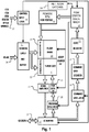
- FIG. 1 is a block diagram of an example of a flash memory integrated circuit including retention check logic and a retention write mode.
- the integrated circuit includes a main flash array 10 having columns of non-volatile, charge trapping memory cells coupled to y-pass gates 11 and rows of cells coupled to an x-decoder 12.
- a y-decoder 13 is coupled to the y-pass gates 11.
- the y-pass gates 11 are coupled via a program data high-voltage circuit PGM DATA HV 14 to program data latches 16, which are in turn coupled to an input-output I/O buffer 17.
- the y-pass gates 11 are coupled to sense amplifiers 15, which are in turn coupled to the input-output I/O buffer 17.
- the integrated circuit includes control input logic 30, an address latch and buffer 31, a command data latch 20, a command data decoder 21, a state register 22, and a state machine 23.
- the integrated circuit also includes program/erase/retention high-voltage circuits 25 which are coupled to the x-decoder 12.
- the state machine 23 is configured to operate in program, erase, read and retention modes as described in more detail below. In this example, the state machine 23 is coupled to a block of retention address latches 24, which can store a queue of addresses subject of a retention write process.
- the control input logic 30 is connected to input pins 35 (CE#, OE#, WE#, RESET#, BYTE#, and WP#/ACC), and creates internal timing control signals to enable the address latch and buffer 31 to latch the external address pins 36 (A0-AM).
- the internal addresses are output from address latch and buffer 31 to the main array and decoders composed of x-decoder 12, y-decoder 13, y-pass gates 11, and flash array 10.
- the x-decoder 12 decodes the word-lines of the flash array, while the y-decoder 13 decodes the bit lines of the flash array.
- the bit lines are electrically connected to the sense amplifiers 15 and program data high-voltage circuit 14 selectively through the y-pass gates 11.
- Sense amplifiers 15 are used to read out the contents of the flash memory, while the program data high-voltage circuit block 14 is used to selectively deliver high power to bit-lines during programming.
- the I/O buffer 17 controls the input and output on the Q0-Q15/A-1 output pads 37. During read operation, the I/O buffer 17 receives data from sense amplifiers 15 and drives the output pads 37 accordingly. In the last cycle of program command, for example, the I/O buffer 17 transmits the data on output pads 37 (Q0-Q15/A-1) to program data latch 16, which controls the high power drivers in program data high-voltage circuit 14 to selectively program the bits in a word or byte according to the user input pattern.
- the program/erase/retention high-voltage circuits 25 comprise the circuits to generate and deliver the necessary high voltage to the x-decoder 12, flash array 10, and program data high-voltage circuit 14 blocks.
- the integrated circuit includes controller circuitry, including a logic control module comprised of the state machine 23, state register 22, command data decoder 21, and command data latch 20.
- controller circuitry including a logic control module comprised of the state machine 23, state register 22, command data decoder 21, and command data latch 20.
- the user signals a command, for example by toggling WE#
- the command on Q0-Q15/A-1 is latched in the command data latch 20 and is decoded by the command data decoder 21.
- the state register 22 receives the command and records the current state of the device.
- the state machine 23 implements the internal algorithms for program or erase according to the current command state by controlling each block in the block diagram.
- the flash memory array can be organized for Byte mode (x8) or Word mode (x16) read and write processes. In other embodiments, the integrated circuit can be configured for page mode read and write.
- the state machine 23 implements retention check algorithms including a retention read check and a retention write as described further below.
- a set of retention address latches 24 is provided as an address buffer which can be utilized to support the retention check processes.
- the retention check processes can be implemented using logic on the integrated circuit apart from the state machine 23.
- the state machine 23, and any separate logic implementing the retention mode algorithms can be implemented, in whole or in part, using dedicated logic circuitry defined using a high-level description language such as Verilog.
- one or more of the algorithms implementing retention check processes, program processes and erase processes can be implemented using an on-chip general purpose processor with suitable software. Also, combinations of dedicated logic and software controlled general-purpose processors can be applied to implement these algorithms.
- the technology described herein comprises an array of memory cells, configured for access by a plurality of word lines and bit lines and to store data values in the memory cells using different threshold states.
- a controller such as state machine 23 and supporting logic are configured in this aspect of the technology for biasing the word and bit lines associated to one of the memory cells to read out the threshold status thereof for example in a stand-by mode or a power-on mode. Retention check operations can take advantage of this stand-by mode read operation, as well as other memory management processes, or processes utilizing the memory for other reasons.
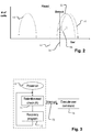
- Figure 2 is a simplified diagram showing distributions of threshold voltages for memory cells in a flash memory array.
- the vertical axis represents the number of cells having a particular threshold voltage (i.e. word line voltage at which the memory cell turns on sufficient for the sensing circuits), while the horizontal axis represents the word line voltage for the corresponding sample.
- threshold voltage i.e. word line voltage at which the memory cell turns on sufficient for the sensing circuits
- horizontal axis represents the word line voltage for the corresponding sample.
- a lower threshold distribution 50 corresponds to the lower threshold memory state for the memory cells in the array.
- a higher threshold distribution 51 corresponds to the higher threshold memory state for the memory cells.
- the memory device applies a read voltage at a voltage level 52 between the lower threshold distribution and the higher threshold distribution 51.
- the range between the maximum threshold voltage for the lower threshold distribution 50, and the minimum threshold voltage for the higher threshold distribution 51 represents a margin for successful reading of the memory cells.
- the retention check can include performing a test read using a read bias that includes a word line voltage such as at the level 54 to detect memory cells which are suffering a charge loss or another condition that leads to a reduction in their threshold voltage.
- the retention read can use other biasing techniques, including for example using a read bias using the same word line voltage as a normal read, while setting sensing biases at the sense amplifier or bit line load circuits to detect cells suffering from threshold drift.
- the retention check can involve detecting such memory cells, and then performing a retention write process represented by the arrow 55, which can increase the threshold voltage of the detected cells. This increase in threshold voltage places the cell threshold further away from the read bias, improving its condition for data retention.
- the retention write process can be the same as a normal program sequence used in response to a program command.
- the retention write can be different from the normal program sequence.
- the retention write may employ different voltages and/or different pulse widths than the normal program sequence.
- the retention write may skip some steps used in normal program sequences. The use of different sequences for retention write than for normal program however can complicate the logic design, and so it may be preferred for some programming technologies, to use the same sequence for both.
- a retention check can be implemented that is executed after a power-on sequence for the device as illustrated in Figure 3 .
- logic on the device executes a retention read check sequence 71 which can detect memory cells in the higher threshold memory state having a threshold voltage below a retention check threshold.
- a retention write sequence 72 can be executed for any cell which fails the retention check.
- the addresses of cells which fail the retention check can be stored, preferably on the device, in case of an interruption before a retention write sequence is executed.
- the retention write sequence 72 can increase the threshold voltage of the cells identified during the retention read check sequence 71.
- This algorithm can continue until it is interrupted by a user command 73.
- the retention mode processing is suspended, such as in response to an interrupt signal, and the user command is executed (74).
- the user command is treated with higher priority than the retention check process, and thereby causes little or no delay during mission functions of the device.
- Typical modes for a flash memory include a read mode, and embedded write mode, and a stand-by mode.
- Retention mode processing can be executed during any of these modes. It can be desirable to execute mission function user commands with higher priority. So, logic is provided to suspend retention check sequences in favor of mission functions.
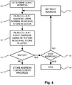
- FIG. 4 illustrates a representative retention check algorithm.
- the retention check algorithm can include a process which determines a start address (80). This start address can be determined randomly on the initiation of the retention check, provided the random start addresses of the retention checks can provide coverage for enough of the memory array to improve performance. In other examples, the start address can be determined algorithmically, using patterns that are likely to cover the entire array, or selected portions of the array, over a certain operating interval. Using random start addresses can simplify the logic needed to support the process, while giving reasonable assurance that all the cells in the memory array will be checked within suitable intervals of time.
- the retention check logic executes a sequence including reading memory cells iteratively across a set of addresses, which may identify a byte, word or page of memory cells for example. For each iteration, the cells are read using a normal read bias and the results stored in a latch if necessary for later processes (81). Also, cells are read using a retention read bias and stored in a latch if necessary for later processes (82). This read at the retention read bias can be limited to only those cells which are in the higher threshold state, as indicated by the read using the normal read bias. The results of the normal read bias read and the retention read bias read are compared (83). If the results do not match, then the retention check logic can store the address for use by a recovery program (84).
- the recovery program can include executing a retention write that comprises a standard program sequence to set a high threshold state in the memory cells which fail the retention read check.
- the recovery program can include a standard read followed by a re-program of the same data values on the byte, word or page level.
- the data from the retention read check which was taken at the normal read bias can be stored for use during the later recovery program.
- the retention read process can store bit addresses, and the recovery program can be limited to individual bits.
- the addresses stored at block 84 can be maintained in a queue of addresses for memory cells requiring a retention recovery program, using on-chip registers or latches for example.
- the retention recovery program can be executed later in time, and results of a retention read check can be maintained even in the event of an interrupt because of a user mode command.
- the retention check logic determines whether the last address in the sequence has been encountered (85). If yes, then this instance of the retention check is completed (86). If the last address in the sequence has not been encountered, then a next address is set (87). Then, a next iteration in the retention check logic is executed starting at block 81.
- the last address used for a given retention check sequence can be set so that each retention check sequence executes over only part of the array, limiting the amount of time that the device stays in a retention check.
- the last address used can be a constant value at the highest or lowest address used to access the array, so that the retention check sequence will continue from the beginning first start address determined at step 80, to the end of the memory array, or until the process is interrupted.
- the retention check process operates in a loop, storing the last address used for restarting the process, with no start or end address. For example, assuming a start address is for address bits A24:A0 equal to hex 123456, then the retention check look can proceed through address 123456, 123457, ..., ffffff, 000000, ...123456 and so on. If an interrupt occurs, for example at address fffffff, the retention check address ffffff is stored for use as a starting address in a next cycle.
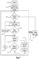
- Figure 5 illustrates a retention check process which can be executed during a stand-by mode on an integrated circuit memory.
- a stand-by retention check address is produced using a random value (101).
- the check address can be produced in other ways as mentioned above.
- the control logic on the chip can enter the stand-by mode after power-on 100. In this case, loop is entered where the logic determines whether the chip remains in stand-by mode (102). If the logic remains in the stand-by mode, then a retention read check process is executed (103). During the retention read check process, the logic determines whether a retention check has failed for a particular address (104).
- next address is provided (105), and the process loops to the next iteration starting at block 103. If at block 104, it is detected that the memory cell at a particular address failed the retention check, then the address of the failed memory cell is stored (106).
- the logic determines whether the chip is ready to enter a retention program mode at step 107.
- the chip is ready if it meets conditions set by the logic, which conditions can depend on such factors as whether there is an address stored, the mode in which the chip is operating and specifications for operation of the chip. For example, the chip may be ready only if it is in stand-by mode.
- a disadvantage of doing the retention program in stand-by mode is that the chip will draw some current which may not be suitable for stand-by conditions.
- the chip may be ready only if it is in user program mode, and the retention flow can be inserted before the user program operation, causing a small latency addition.
- the algorithm can idle 108 to await program ready status. If the program is ready at step 107, then an address from the queue of addresses stored in the buffer and generated using the retention check is loaded (110), and a program operation is executed as a retention write (111). After the program operation as step 111, the logic can return to a wait state, in which it waits for the next time the controller enters the stand-by mode, as indicated by the loop to block 102.
- the retention check logic is not invoked, and rather as indicated at block 102, the user mode is executed as indicated by the command (121). If at power on, there is no user command, then the stand-by mode is entered, and the logic follows the branch at block 102 to perform the retention check. Also, at any time during the retention check, if a user command is received, then the process is interrupted (120) and the user command is executed (121).
- FIG. 6 is a flowchart for a write process which has been modified to support retention check logic as described herein.
- the retention recovery step can be part of an embedded write command.
- the device can be configured to begin a write process upon receipt of a user mode write command for a specific program address (150).
- the logic can determine whether an address for a cell that fails the retention check process is ready for reprogramming (151). If there are addresses ready for retention reprogramming, then those addresses are queued with the program address carried by the command for retention write during the program sequence (152).
- the program sequence executes a user write using the program address carried by the program command (153).
- the program sequence also executes a retention write using the retention address stored in the retention address queue (154). After both write sequences have been performed, the program mode command is completed (155).
- Figure 7 is a simplified state diagram for an integrated circuit which implements retention logic as described herein.
- the integrated circuit has a power-on mode 200, a stand-by mode 201, a write mode 202, and a read mode 203.
- the control logic transitions 210 to the stand-by mode 201, unless a read or write command is received. If a read or write command is received, then the control logic transitions 212 to the read mode 203 or transitions 211 to the write mode 202 as appropriate. After a write process in the write mode 202 is executed, then the logic can transition 218 to the stand-by mode 201.
- the logic can transition 213 to the read mode 203.
- the logic can transition 217 to the stand-by mode 201.
- logic can transition 213 to the write mode 202.
- the control logic can execute the retention check and retention write algorithms as indicated by loop 214.
- the control logic on the chip during the power-on mode 200 can execute the retention check and retention write algorithms as indicated by loop 215.
- control logic can be configured to execute the retention check and retention write algorithms both during the power-on mode 200 and during the stand-by mode 201. Also, during a write mode 202, the logic can execute retention write algorithms is indicated by the loop 216.
- the retention check and retention write algorithms can be executed by the on chip controller, for example, in non-user command modes.
- a non-user command mode is a mode such as stand-by mode, in which the memory is not being accessed in performance of a user command, and is therefore available for access in performance of the retention check and retention write algorithms
- the examples described herein involve memory cells configured to store one bit per cell.
- the technology can be applied as well to multi-level cells, or cells that store more than one bit per cell using a sequence of retention check reads at a corresponding sequence of retention read levels.
Description
- The present invention relates to integrated circuit memory, and more particularly to data retention issues arising in non-volatile memory.
- In flash memory devices, data is stored by trapping charge that establishes a cell threshold in memory cells. By sensing the cell threshold, data values can be read. However, as the memory cell sizes are reduced, charge retention, and therefore data retention, can suffer. In non-volatile memory devices configured to store data for long periods of time and through power-on/off events, data retention is an important performance factor. The
US 2008/055997 A1 discloses a flash memory device including a memory cell array comprising memory cells arranged in rows and columns, a page buffer circuit having a single latch structure and configured to read data from a selected page in the memory cell array, and a controller controlling the page buffer circuit to detect memory cells having an improper voltage distribution caused by charge leakage within the selected page. TheUS 2013/007344 A1 discloses an apparatus, a system, and a method for a refreshing of a non-volatile memory. The method comprises a loading of a time stamp, corresponding to data in a data location of a non-volatile memory, to a register; a determining of an elapsed time, corresponding to the data in the data location, according to the loaded time stamp; and a refreshing of the data of the data location for which it is determined that the elapsed time exceeds a refresh time associated with the non-volatile memory. TheUS 2008/068912 A1 discloses a method for a refreshing of a flash memory device including providing first and second refresh fields that include a plurality of memory blocks, and determining, when there is a request for a refresh, a condition of a memory block to be refreshed in accordance with which of the first and second refresh fields includes the memory block to be refreshed. TheUS 2012/008394 A1 discloses a memory system including non-volatile memory devices and a corresponding refresh method. The method groups memory blocks of the non-volatile memory devices into memory groups, determines a refresh sequence for the memory groups, and refreshes the memory groups in accordance with the refresh sequence. TheUS 5 57 ,684 A discloses a flash memory and its data refresh method, where the data read out in a program verify mode and an erase verify mode from the read address are compared in each address, and the data of a memory cell corresponding to the inconsistent data are rewritten, or adding values of the data read out in the program verify mode and the erase verify mode are compared in each block and a defective block is retrieved and the data in each address are compared in the defective block, and the data of a memory cell corresponding to the inconsistent data are rewritten. Thereby, defective data can be retrieved and corrected. TheEP 1 253 599 A1 - It is desirable to provide technologies to improve non-volatile memory performance, and, in general, to improve data retention for integrated circuit memory.
- The object of the present invention is solved for a non-volatile memory device according to the preamble of the
independent apparatus claims 1 by the features of the characterizing part of theindependent apparatus claim 1. In addition, the object of the present invention is solved for a method of operating a non-volatile memory device according to the preamble of the independent method claims 7 by the features of the characterizing part of the independent method claim 7. Non-volatile memory is described which includes retention check logic. The memory can comprise an integrated circuit having an array of memory cells configured to store data values using threshold states, including a higher threshold state characterized as exceeding a selected read bias. A controller includes retention check logic to identify memory cells in the higher threshold state which fail a threshold retention check, and logic to improve the threshold of the identified memory cells, such as by programming. - Other aspects and advantages of the present technology can be seen on review of the drawings, the detailed description and the claims, which follow.
-
-
Figure 1 is a simplified block diagram of an example of a flash memory integrated circuit implementing retention check logic. -
Figure 2 is a simplified graph showing threshold voltage ranges for lower and higher threshold voltage states of single bit flash memory cells. -
Figure 3 is a simplified diagram of a retention check logic executed upon a power-on event on an integrated circuit memory. -
Figure 4 is a simplified flow diagram for retention check logic which can be implemented on an integrated circuit memory. -
Figure 5 is a simplified flow diagram for a retention check logic executed in a stand-by mode on an integrated circuit memory. -
Figure 6 is a simplified diagram of a modified write process implemented to support retention check logic as described herein. -
Figure 7 is a simplified state diagram for an integrated circuit controller executing retention check logic as described herein. - A detailed description of embodiments of the present invention is provided with reference to the
Figures 1-7 . -
Figure 1 is a block diagram of an example of a flash memory integrated circuit including retention check logic and a retention write mode. Schematically, the integrated circuit includes amain flash array 10 having columns of non-volatile, charge trapping memory cells coupled to y-pass gates 11 and rows of cells coupled to anx-decoder 12. A y-decoder 13 is coupled to the y-pass gates 11. The y-pass gates 11 are coupled via a program data high-voltage circuitPGM DATA HV 14 toprogram data latches 16, which are in turn coupled to an input-output I/O buffer 17. Also, the y-pass gates 11 are coupled to senseamplifiers 15, which are in turn coupled to the input-output I/O buffer 17. The integrated circuit includescontrol input logic 30, an address latch andbuffer 31, acommand data latch 20, acommand data decoder 21, astate register 22, and astate machine 23. The integrated circuit also includes program/erase/retention high-voltage circuits 25 which are coupled to thex-decoder 12. Thestate machine 23 is configured to operate in program, erase, read and retention modes as described in more detail below. In this example, thestate machine 23 is coupled to a block ofretention address latches 24, which can store a queue of addresses subject of a retention write process. - The
control input logic 30 is connected to input pins 35 (CE#, OE#, WE#, RESET#, BYTE#, and WP#/ACC), and creates internal timing control signals to enable the address latch and buffer 31 to latch the external address pins 36 (A0-AM). The internal addresses are output from address latch andbuffer 31 to the main array and decoders composed ofx-decoder 12, y-decoder 13, y-pass gates 11, andflash array 10. Thex-decoder 12 decodes the word-lines of the flash array, while the y-decoder 13 decodes the bit lines of the flash array. The bit lines are electrically connected to thesense amplifiers 15 and program data high-voltage circuit 14 selectively through the y-pass gates 11.Sense amplifiers 15 are used to read out the contents of the flash memory, while the program data high-voltage circuit block 14 is used to selectively deliver high power to bit-lines during programming. The I/O buffer 17 controls the input and output on the Q0-Q15/A-1 output pads 37. During read operation, the I/O buffer 17 receives data fromsense amplifiers 15 and drives theoutput pads 37 accordingly. In the last cycle of program command, for example, the I/O buffer 17 transmits the data on output pads 37 (Q0-Q15/A-1) to programdata latch 16, which controls the high power drivers in program data high-voltage circuit 14 to selectively program the bits in a word or byte according to the user input pattern. - The program/erase/retention high-
voltage circuits 25 comprise the circuits to generate and deliver the necessary high voltage to thex-decoder 12,flash array 10, and program data high-voltage circuit 14 blocks. - The integrated circuit includes controller circuitry, including a logic control module comprised of the
state machine 23,state register 22,command data decoder 21, andcommand data latch 20. When the user signals a command, for example by toggling WE#, the command on Q0-Q15/A-1 is latched in thecommand data latch 20 and is decoded by thecommand data decoder 21. Thestate register 22 receives the command and records the current state of the device. Thestate machine 23 implements the internal algorithms for program or erase according to the current command state by controlling each block in the block diagram. The flash memory array can be organized for Byte mode (x8) or Word mode (x16) read and write processes. In other embodiments, the integrated circuit can be configured for page mode read and write. - Also, the
state machine 23 implements retention check algorithms including a retention read check and a retention write as described further below. In support of the retention check algorithms, a set ofretention address latches 24 is provided as an address buffer which can be utilized to support the retention check processes. In other embodiments, the retention check processes can be implemented using logic on the integrated circuit apart from thestate machine 23. In some implementations, thestate machine 23, and any separate logic implementing the retention mode algorithms, can be implemented, in whole or in part, using dedicated logic circuitry defined using a high-level description language such as Verilog. In other implementations, one or more of the algorithms implementing retention check processes, program processes and erase processes can be implemented using an on-chip general purpose processor with suitable software. Also, combinations of dedicated logic and software controlled general-purpose processors can be applied to implement these algorithms. - In one aspect, the technology described herein comprises an array of memory cells, configured for access by a plurality of word lines and bit lines and to store data values in the memory cells using different threshold states. A controller, such as
state machine 23 and supporting logic are configured in this aspect of the technology for biasing the word and bit lines associated to one of the memory cells to read out the threshold status thereof for example in a stand-by mode or a power-on mode. Retention check operations can take advantage of this stand-by mode read operation, as well as other memory management processes, or processes utilizing the memory for other reasons. -
Figure 2 is a simplified diagram showing distributions of threshold voltages for memory cells in a flash memory array. The vertical axis represents the number of cells having a particular threshold voltage (i.e. word line voltage at which the memory cell turns on sufficient for the sensing circuits), while the horizontal axis represents the word line voltage for the corresponding sample. For a single bit memory cell, there are two threshold distributions which are used to represent data values. Alower threshold distribution 50 corresponds to the lower threshold memory state for the memory cells in the array. Ahigher threshold distribution 51 corresponds to the higher threshold memory state for the memory cells. In a read mode, the memory device applies a read voltage at avoltage level 52 between the lower threshold distribution and thehigher threshold distribution 51. The range between the maximum threshold voltage for thelower threshold distribution 50, and the minimum threshold voltage for thehigher threshold distribution 51 represents a margin for successful reading of the memory cells. - In floating gate and charge trapping flash memory, as the technology progressively scales down in size, data retention may suffer because of charge leakage. Also, data retention can be an issue for other memory types. Data retention can suffer if the threshold voltages of the memory cells in the array drift during the life of the device. This phenomenon is represented by the shifted
threshold distribution 53 shown inFigure 2 , where the memory cells that use trapped charge to set the threshold may lose charge over time, particularly when they are in the higher threshold state, resulting in a shift in their threshold voltage. This shift in the threshold voltage reduces the margin, and can cause reliability problems. - As described herein, logic is provided to perform a retention check of memory cells in a memory array. The retention check can include performing a test read using a read bias that includes a word line voltage such as at the
level 54 to detect memory cells which are suffering a charge loss or another condition that leads to a reduction in their threshold voltage. Alternatively, the retention read can use other biasing techniques, including for example using a read bias using the same word line voltage as a normal read, while setting sensing biases at the sense amplifier or bit line load circuits to detect cells suffering from threshold drift. The retention check can involve detecting such memory cells, and then performing a retention write process represented by thearrow 55, which can increase the threshold voltage of the detected cells. This increase in threshold voltage places the cell threshold further away from the read bias, improving its condition for data retention. - The retention write process can be the same as a normal program sequence used in response to a program command. Alternatively, the retention write can be different from the normal program sequence. For example, the retention write may employ different voltages and/or different pulse widths than the normal program sequence. Also, the retention write may skip some steps used in normal program sequences. The use of different sequences for retention write than for normal program however can complicate the logic design, and so it may be preferred for some programming technologies, to use the same sequence for both.
- In order to improve data retention, a retention check can be implemented that is executed after a power-on sequence for the device as illustrated in
Figure 3 . According to the retention check shown inFigure 3 , when the device powers on (70), logic on the device executes a retention readcheck sequence 71 which can detect memory cells in the higher threshold memory state having a threshold voltage below a retention check threshold. After the retention readcheck sequence 71, or in a parallel or pipelined fashion, aretention write sequence 72 can be executed for any cell which fails the retention check. The addresses of cells which fail the retention check can be stored, preferably on the device, in case of an interruption before a retention write sequence is executed. Theretention write sequence 72 can increase the threshold voltage of the cells identified during the retention readcheck sequence 71. This algorithm can continue until it is interrupted by auser command 73. Upon detection of a user command, the retention mode processing is suspended, such as in response to an interrupt signal, and the user command is executed (74). In this manner, the user command is treated with higher priority than the retention check process, and thereby causes little or no delay during mission functions of the device. - Typical modes for a flash memory include a read mode, and embedded write mode, and a stand-by mode. Retention mode processing can be executed during any of these modes. It can be desirable to execute mission function user commands with higher priority. So, logic is provided to suspend retention check sequences in favor of mission functions.
-
Figure 4 illustrates a representative retention check algorithm. The retention check algorithm can include a process which determines a start address (80). This start address can be determined randomly on the initiation of the retention check, provided the random start addresses of the retention checks can provide coverage for enough of the memory array to improve performance. In other examples, the start address can be determined algorithmically, using patterns that are likely to cover the entire array, or selected portions of the array, over a certain operating interval. Using random start addresses can simplify the logic needed to support the process, while giving reasonable assurance that all the cells in the memory array will be checked within suitable intervals of time. - After determining a start address, the retention check logic executes a sequence including reading memory cells iteratively across a set of addresses, which may identify a byte, word or page of memory cells for example. For each iteration, the cells are read using a normal read bias and the results stored in a latch if necessary for later processes (81). Also, cells are read using a retention read bias and stored in a latch if necessary for later processes (82). This read at the retention read bias can be limited to only those cells which are in the higher threshold state, as indicated by the read using the normal read bias. The results of the normal read bias read and the retention read bias read are compared (83). If the results do not match, then the retention check logic can store the address for use by a recovery program (84). The recovery program can include executing a retention write that comprises a standard program sequence to set a high threshold state in the memory cells which fail the retention read check. The recovery program can include a standard read followed by a re-program of the same data values on the byte, word or page level. In an alternative, the data from the retention read check which was taken at the normal read bias can be stored for use during the later recovery program. In yet other embodiments, the retention read process can store bit addresses, and the recovery program can be limited to individual bits.
- The addresses stored at
block 84 can be maintained in a queue of addresses for memory cells requiring a retention recovery program, using on-chip registers or latches for example. In this case, the retention recovery program can be executed later in time, and results of a retention read check can be maintained even in the event of an interrupt because of a user mode command. - If the results match at the test in
step 83, then the retention check logic determines whether the last address in the sequence has been encountered (85). If yes, then this instance of the retention check is completed (86). If the last address in the sequence has not been encountered, then a next address is set (87). Then, a next iteration in the retention check logic is executed starting atblock 81. The last address used for a given retention check sequence can be set so that each retention check sequence executes over only part of the array, limiting the amount of time that the device stays in a retention check. Alternatively, the last address used can be a constant value at the highest or lowest address used to access the array, so that the retention check sequence will continue from the beginning first start address determined atstep 80, to the end of the memory array, or until the process is interrupted. In yet another alternative, the retention check process operates in a loop, storing the last address used for restarting the process, with no start or end address. For example, assuming a start address is for address bits A24:A0 equal to hex 123456, then the retention check look can proceed through address 123456, 123457, ..., ffffff, 000000, ...123456 and so on. If an interrupt occurs, for example at address ffffff, the retention check address ffffff is stored for use as a starting address in a next cycle. -
Figure 5 illustrates a retention check process which can be executed during a stand-by mode on an integrated circuit memory. In this example, after a power-onevent 100, a stand-by retention check address is produced using a random value (101). The check address can be produced in other ways as mentioned above. The control logic on the chip can enter the stand-by mode after power-on 100. In this case, loop is entered where the logic determines whether the chip remains in stand-by mode (102). If the logic remains in the stand-by mode, then a retention read check process is executed (103). During the retention read check process, the logic determines whether a retention check has failed for a particular address (104). If the retention check does not fail for the particular address, then the next address is provided (105), and the process loops to the next iteration starting atblock 103. If atblock 104, it is detected that the memory cell at a particular address failed the retention check, then the address of the failed memory cell is stored (106). - The logic determines whether the chip is ready to enter a retention program mode at
step 107. The chip is ready if it meets conditions set by the logic, which conditions can depend on such factors as whether there is an address stored, the mode in which the chip is operating and specifications for operation of the chip. For example, the chip may be ready only if it is in stand-by mode. A disadvantage of doing the retention program in stand-by mode is that the chip will draw some current which may not be suitable for stand-by conditions. Alternatively, or in addition, the chip may be ready only if it is in user program mode, and the retention flow can be inserted before the user program operation, causing a small latency addition. - If the chip is not ready at
step 107, then the algorithm can idle 108 to await program ready status. If the program is ready atstep 107, then an address from the queue of addresses stored in the buffer and generated using the retention check is loaded (110), and a program operation is executed as a retention write (111). After the program operation as step 111, the logic can return to a wait state, in which it waits for the next time the controller enters the stand-by mode, as indicated by the loop to block 102. - If the power-on event is accompanied by a user command, then the retention check logic is not invoked, and rather as indicated at
block 102, the user mode is executed as indicated by the command (121). If at power on, there is no user command, then the stand-by mode is entered, and the logic follows the branch atblock 102 to perform the retention check. Also, at any time during the retention check, if a user command is received, then the process is interrupted (120) and the user command is executed (121). -
Figure 6 is a flowchart for a write process which has been modified to support retention check logic as described herein. In the case in which the addresses of memory cells which fail retention check have been stored in a buffer, and have not been reprogrammed due to an interrupt or for other reasons, the retention recovery step can be part of an embedded write command. In this example, as shown inFigure 6 , the device can be configured to begin a write process upon receipt of a user mode write command for a specific program address (150). During the write process, the logic can determine whether an address for a cell that fails the retention check process is ready for reprogramming (151). If there are addresses ready for retention reprogramming, then those addresses are queued with the program address carried by the command for retention write during the program sequence (152). The program sequence executes a user write using the program address carried by the program command (153). The program sequence also executes a retention write using the retention address stored in the retention address queue (154). After both write sequences have been performed, the program mode command is completed (155). -
Figure 7 is a simplified state diagram for an integrated circuit which implements retention logic as described herein. In this simplified example, the integrated circuit has a power-onmode 200, a stand-by mode 201, awrite mode 202, and aread mode 203. When power is supplied to the device, it enters the power-onmode 200. After the power-on sequence, thecontrol logic transitions 210 to the stand-by mode 201, unless a read or write command is received. If a read or write command is received, then thecontrol logic transitions 212 to theread mode 203 ortransitions 211 to thewrite mode 202 as appropriate. After a write process in thewrite mode 202 is executed, then the logic can transition 218 to the stand-by mode 201. Also, from thewrite mode 202 for particular write commands, or if a read command is received during a write process, the logic can transition 213 to theread mode 203. Likewise, after a read process in theread mode 203, the logic can transition 217 to the stand-by mode 201. Also, from the readmode 203, for particular types of commands, or if a write command is received during a read process, logic can transition 213 to thewrite mode 202. As described above, during the stand-by mode 201 the control logic can execute the retention check and retention write algorithms as indicated byloop 214. In the alternative, the control logic on the chip during the power-onmode 200 can execute the retention check and retention write algorithms as indicated byloop 215. In some embodiments, the control logic can be configured to execute the retention check and retention write algorithms both during the power-onmode 200 and during the stand-by mode 201. Also, during awrite mode 202, the logic can execute retention write algorithms is indicated by theloop 216. In general, the retention check and retention write algorithms can be executed by the on chip controller, for example, in non-user command modes. A non-user command mode is a mode such as stand-by mode, in which the memory is not being accessed in performance of a user command, and is therefore available for access in performance of the retention check and retention write algorithms - The examples described herein involve memory cells configured to store one bit per cell. The technology can be applied as well to multi-level cells, or cells that store more than one bit per cell using a sequence of retention check reads at a corresponding sequence of retention read levels.
Claims (8)
- A non-volatile memory device, comprising:a flash array (10) of memory cells, configured to store data values in memory cells in the flash array (10) using threshold states, including a higher threshold state having a minimum threshold exceeding a selected read bias; anda controller including a retention check logic configured to identify memory cells in the higher threshold state having threshold voltages which fail a retention threshold check, and including a logic configured to execute, upon power-on of the memory device, a retention write (72) on the identified memory cells in the higher threshold state,characterized in thatthe retention check logic is configured to execute a sequence including a reading of memory cells iteratively across addresses, where the iterative reading includes a reading of a memory cell at an address using a first read bias configured to read the data values stored in the memory cells, a determining of comparative values from the memory cells using a second read bias configured to indicate whether the memory cells having the higher threshold state have a threshold voltage lower than a specified retention threshold, a comparing of the data values and the comparative values, and if there is not a match a storing of the address of the identified memory cell.
- The non-volatile memory device of claim 1, wherein the controller is configured to store addresses of memory cells which fail the retention check, and includes a logic to enter a program mode in response to a user command, wherein the program mode is configured to write data to selected cells, and to queue the stored addresses for a programming to the high threshold state.
- The non-volatile memory device of any of the claims 1 and 2, wherein the controller is configured to interrupt the logic to identify memory cells which fail the threshold retention check if a read or program command is received.
- The non-volatile memory device of any of the claims 1 to 3, wherein the memory cells in the flash array (10) of memory cells are charge trapping memory cells, the controller includes a stand-by mode, a write mode and a read mode, and wherein the retention check logic is executed during the stand-by mode.
- The non-volatile memory device of any of the claims 1 to 4, wherein the controller is configured to interrupt the retention check logic if a user command is received.
- A method of operating a non-volatile memory device having a flash array (10) of memory cells configured to store data values in memory cells in the flash array (10) using threshold states, including a higher threshold state, comprising:identifying memory cells in the higher threshold state which have threshold voltages which fail a retention threshold check (71); andperforming, upon power-on (70) of the memory device, of a retention write process (72) on the memory cells identified as a result of the retention check (71),characterized in thatsaid identifying step includes reading memory cells iteratively across addresses, where an iteration includes reading a memory cell at an address using a first read bias configured to read the data values stored in the memory cells, determining comparative values from the memory cells using a second read bias configured to indicate whether the memory cells having the higher threshold state have a threshold voltage lower than the specified retention threshold, comparing the data values and the comparative values, and if there is not a match storing the address of the identified memory cell.
- The method of claim 6, including storing addresses of the identified memory cells, and in a program mode entered in response to a user command, wherein the program mode is configured to write data to selected cells, and queuing the stored addresses for programming to the high threshold state.
- The method of any of the claims 6 and 7, including interrupting said identifying step if a read or program command is received.
Applications Claiming Priority (1)
| Application Number | Priority Date | Filing Date | Title |
|---|---|---|---|
| US201361780942P | 2013-03-13 | 2013-03-13 |
Publications (3)
| Publication Number | Publication Date |
|---|---|
| EP2779175A2 EP2779175A2 (en) | 2014-09-17 |
| EP2779175A3 EP2779175A3 (en) | 2014-12-31 |
| EP2779175B1 true EP2779175B1 (en) | 2018-11-28 |
Family
ID=48700438
Family Applications (1)
| Application Number | Title | Priority Date | Filing Date |
|---|---|---|---|
| EP13174686.9A Active EP2779175B1 (en) | 2013-03-13 | 2013-07-02 | Retention check logic for non-volatile memory |
Country Status (6)
| Country | Link |
|---|---|
| US (2) | US9147501B2 (en) |
| EP (1) | EP2779175B1 (en) |
| JP (1) | JP6081878B2 (en) |
| KR (2) | KR20140112349A (en) |
| CN (1) | CN104051018B (en) |
| TW (1) | TWI498897B (en) |
Families Citing this family (12)
| Publication number | Priority date | Publication date | Assignee | Title |
|---|---|---|---|---|
| US9147501B2 (en) | 2013-03-13 | 2015-09-29 | Macronix International Co., Ltd. | Retention logic for non-volatile memory |
| TWI515743B (en) * | 2013-11-20 | 2016-01-01 | 旺宏電子股份有限公司 | Method, electronic device and controller for recovering array of memory cells |
| US9595342B2 (en) | 2015-01-20 | 2017-03-14 | Sandisk Technologies Llc | Method and apparatus for refresh programming of memory cells based on amount of threshold voltage downshift |
| US9727261B2 (en) | 2015-09-24 | 2017-08-08 | Western Digital Technologies, Inc. | Weighted programming patterns in solid-state data storage systems |
| KR102444604B1 (en) | 2016-02-02 | 2022-09-21 | 에스케이하이닉스 주식회사 | Data storage device and operating method thereof |
| US10658046B2 (en) * | 2017-05-26 | 2020-05-19 | Macronix International Co., Ltd. | Memory device and method for operating the same |
| US10459836B2 (en) | 2017-06-22 | 2019-10-29 | Macronix International Co., Ltd. | Memory device and associated control method |
| CN108847268B (en) * | 2018-06-13 | 2020-10-16 | 上海华力微电子有限公司 | Threshold voltage adjusting method and system of storage unit model |
| KR102499061B1 (en) | 2018-08-22 | 2023-02-13 | 삼성전자주식회사 | Semiconductor memory device including phase change memory device and method of accessing phase change memory device |
| JP2021044033A (en) | 2019-09-09 | 2021-03-18 | キオクシア株式会社 | Semiconductor storage device |
| KR20210103234A (en) | 2020-02-13 | 2021-08-23 | 에스케이하이닉스 주식회사 | Controller and operating method thereof |
| JP2021174564A (en) | 2020-04-24 | 2021-11-01 | キオクシア株式会社 | Semiconductor storage device |
Citations (1)
| Publication number | Priority date | Publication date | Assignee | Title |
|---|---|---|---|---|
| US20050270842A1 (en) * | 2004-06-08 | 2005-12-08 | Nec Electronics Corporation | Nonvolatile memory |
Family Cites Families (28)
| Publication number | Priority date | Publication date | Assignee | Title |
|---|---|---|---|---|
| JPH08190796A (en) | 1995-01-09 | 1996-07-23 | Mitsubishi Denki Semiconductor Software Kk | Flash memory having data refreshing function and data refreshing method for flash memory |
| US5835429A (en) * | 1997-05-09 | 1998-11-10 | Lsi Logic Corporation | Data retention weak write circuit and method of using same |
| JP2000228094A (en) * | 1999-02-04 | 2000-08-15 | Toshiba Corp | Non-volatile semiconductor memory |
| US6636440B2 (en) | 2001-04-25 | 2003-10-21 | Saifun Semiconductors Ltd. | Method for operation of an EEPROM array, including refresh thereof |
| US6882567B1 (en) * | 2002-12-06 | 2005-04-19 | Multi Level Memory Technology | Parallel programming of multiple-bit-per-cell memory cells on a continuous word line |
| JP2005078489A (en) * | 2003-09-02 | 2005-03-24 | Toshiba Lsi System Support Kk | Microcontroller and its control method |
| JP2006338789A (en) * | 2005-06-02 | 2006-12-14 | Renesas Technology Corp | Nonvolatile semiconductor memory device |
| US7457163B2 (en) * | 2006-06-01 | 2008-11-25 | Sandisk Corporation | System for verifying non-volatile storage using different voltages |
| FR2904464A1 (en) * | 2006-07-27 | 2008-02-01 | St Microelectronics Sa | EEPROM LOAD RETENTION CIRCUIT FOR TIME MEASUREMENT |
| KR100794664B1 (en) | 2006-09-01 | 2008-01-14 | 삼성전자주식회사 | Flash memory device and refresh method thereof |
| KR100875292B1 (en) | 2006-09-19 | 2008-12-23 | 삼성전자주식회사 | Flash memory device and its refresh method |
| KR100830580B1 (en) * | 2006-10-20 | 2008-05-21 | 삼성전자주식회사 | Data restore method of memory system including flash memory device |
| US7729193B2 (en) * | 2007-08-10 | 2010-06-01 | Maxim Integrated Products, Inc. | Backup for volatile state retention in the absence of primary circuit power |
| KR101490426B1 (en) * | 2008-11-14 | 2015-02-06 | 삼성전자주식회사 | Nonvolatile memory device and read method thereof |
| KR101026385B1 (en) * | 2009-01-06 | 2011-04-07 | 주식회사 하이닉스반도체 | Operation method of charge trapping type flash memory device |
| KR101612298B1 (en) * | 2009-03-13 | 2016-04-14 | 삼성전자주식회사 | Power gating circuit and integrated circuit including the same |
| US8365030B1 (en) * | 2009-03-30 | 2013-01-29 | Samsung Electronics Co., Ltd. | Nonvolatile memory devices and error correction methods thereof |
| US8213236B1 (en) * | 2009-04-21 | 2012-07-03 | Marvell International Ltd. | Flash memory |
| US8238149B2 (en) | 2009-06-25 | 2012-08-07 | Macronix International Co., Ltd. | Methods and apparatus for reducing defect bits in phase change memory |
| US8456214B2 (en) * | 2009-11-17 | 2013-06-04 | Arm Limited | State retention circuit and method of operation of such a circuit |
| CN102783101A (en) * | 2010-03-25 | 2012-11-14 | 日本电气株式会社 | Load balance control unit, load balance control method, and storage medium |
| KR101577721B1 (en) | 2010-07-09 | 2015-12-29 | 삼성전자주식회사 | Memory system and refresh method thereof |
| US8693258B2 (en) * | 2011-03-17 | 2014-04-08 | Densbits Technologies Ltd. | Obtaining soft information using a hard interface |
| US8650353B2 (en) | 2011-07-01 | 2014-02-11 | Intel Corporation | Apparatus, system, and method for refreshing non-volatile memory |
| JP2013041634A (en) * | 2011-08-11 | 2013-02-28 | Fujitsu Ltd | Nonvolatile semiconductor memory device |
| US8838881B2 (en) * | 2012-03-01 | 2014-09-16 | Seagate Technology Llc | Transfer command with specified sense threshold vector component |
| KR20140030569A (en) * | 2012-09-03 | 2014-03-12 | 에스케이하이닉스 주식회사 | Nonvolatile memory device and operating method thereof |
| US9147501B2 (en) | 2013-03-13 | 2015-09-29 | Macronix International Co., Ltd. | Retention logic for non-volatile memory |
-
2013
- 2013-05-28 US US13/903,574 patent/US9147501B2/en active Active
- 2013-06-24 KR KR1020130072261A patent/KR20140112349A/en active Search and Examination
- 2013-07-02 EP EP13174686.9A patent/EP2779175B1/en active Active
- 2013-07-02 JP JP2013139325A patent/JP6081878B2/en active Active
- 2013-07-12 CN CN201310293667.0A patent/CN104051018B/en active Active
- 2013-07-15 TW TW102125165A patent/TWI498897B/en active
-
2015
- 2015-09-28 US US14/867,660 patent/US9514834B2/en active Active
-
2020
- 2020-03-12 KR KR1020200030809A patent/KR102198436B1/en active IP Right Grant
Patent Citations (1)
| Publication number | Priority date | Publication date | Assignee | Title |
|---|---|---|---|---|
| US20050270842A1 (en) * | 2004-06-08 | 2005-12-08 | Nec Electronics Corporation | Nonvolatile memory |
Also Published As
| Publication number | Publication date |
|---|---|
| JP2014179154A (en) | 2014-09-25 |
| CN104051018A (en) | 2014-09-17 |
| US9147501B2 (en) | 2015-09-29 |
| TWI498897B (en) | 2015-09-01 |
| EP2779175A3 (en) | 2014-12-31 |
| TW201435876A (en) | 2014-09-16 |
| US9514834B2 (en) | 2016-12-06 |
| US20160027522A1 (en) | 2016-01-28 |
| JP6081878B2 (en) | 2017-02-15 |
| KR102198436B1 (en) | 2021-01-06 |
| US20140281768A1 (en) | 2014-09-18 |
| EP2779175A2 (en) | 2014-09-17 |
| KR20200032676A (en) | 2020-03-26 |
| CN104051018B (en) | 2018-01-30 |
| KR20140112349A (en) | 2014-09-23 |
Similar Documents
| Publication | Publication Date | Title |
|---|---|---|
| EP2779175B1 (en) | Retention check logic for non-volatile memory | |
| US7701764B2 (en) | Apparatus and method for reduced peak power consumption during common operation of multi-NAND flash memory devices | |
| KR101596827B1 (en) | Nonvolatile memory device method of operating the same and memory system including the same | |
| US7463520B2 (en) | Memory device with variable trim settings | |
| US7466600B2 (en) | System and method for initiating a bad block disable process in a non-volatile memory | |
| US7877668B2 (en) | Memory access system | |
| US7542354B2 (en) | Reprogrammable nonvolatile memory devices and methods | |
| US7652948B2 (en) | Nonvolatile memory devices and programming methods using subsets of columns | |
| KR20120092561A (en) | Interruptible nand flash memory | |
| US6981188B2 (en) | Non-volatile memory device with self test | |
| TWI506424B (en) | Methods and memory devices where a host is used to configure the memory devices to perform an automatic background operation | |
| JP2006190459A (en) | Flash memory device configured to shorten read time, and reading method for the same | |
| US8199577B2 (en) | Ripple programming of memory cells in a nonvolatile memory | |
| JP2005078489A (en) | Microcontroller and its control method | |
| US20220293194A1 (en) | Modulation of source voltage in nand-flash array read | |
| JP2003007074A (en) | Non-volatile semiconductor memory |
Legal Events
| Date | Code | Title | Description |
|---|---|---|---|
| PUAI | Public reference made under article 153(3) epc to a published international application that has entered the european phase |
Free format text: ORIGINAL CODE: 0009012 |
|
| 17P | Request for examination filed |
Effective date: 20130702 |
|
| AK | Designated contracting states |
Kind code of ref document: A2 Designated state(s): AL AT BE BG CH CY CZ DE DK EE ES FI FR GB GR HR HU IE IS IT LI LT LU LV MC MK MT NL NO PL PT RO RS SE SI SK SM TR |
|
| AX | Request for extension of the european patent |
Extension state: BA ME |
|
| PUAL | Search report despatched |
Free format text: ORIGINAL CODE: 0009013 |
|
| AK | Designated contracting states |
Kind code of ref document: A3 Designated state(s): AL AT BE BG CH CY CZ DE DK EE ES FI FR GB GR HR HU IE IS IT LI LT LU LV MC MK MT NL NO PL PT RO RS SE SI SK SM TR |
|
| AX | Request for extension of the european patent |
Extension state: BA ME |
|
| RIC1 | Information provided on ipc code assigned before grant |
Ipc: G11C 16/34 20060101AFI20141126BHEP |
|
| R17P | Request for examination filed (corrected) |
Effective date: 20150609 |
|
| RBV | Designated contracting states (corrected) |
Designated state(s): AL AT BE BG CH CY CZ DE DK EE ES FI FR GB GR HR HU IE IS IT LI LT LU LV MC MK MT NL NO PL PT RO RS SE SI SK SM TR |
|
| STAA | Information on the status of an ep patent application or granted ep patent |
Free format text: STATUS: EXAMINATION IS IN PROGRESS |
|
| 17Q | First examination report despatched |
Effective date: 20161128 |
|
| REG | Reference to a national code |
Ref country code: DE Ref legal event code: R079 Ref document number: 602013047373 Country of ref document: DE Free format text: PREVIOUS MAIN CLASS: G11C0016340000 Ipc: G11C0029500000 |
|
| GRAP | Despatch of communication of intention to grant a patent |
Free format text: ORIGINAL CODE: EPIDOSNIGR1 |
|
| STAA | Information on the status of an ep patent application or granted ep patent |
Free format text: STATUS: GRANT OF PATENT IS INTENDED |
|
| RIC1 | Information provided on ipc code assigned before grant |
Ipc: G11C 29/12 20060101ALI20180529BHEP Ipc: G11C 16/34 20060101ALI20180529BHEP Ipc: G11C 29/50 20060101AFI20180529BHEP |
|
| INTG | Intention to grant announced |
Effective date: 20180614 |
|
| GRAS | Grant fee paid |
Free format text: ORIGINAL CODE: EPIDOSNIGR3 |
|
| GRAA | (expected) grant |
Free format text: ORIGINAL CODE: 0009210 |
|
| STAA | Information on the status of an ep patent application or granted ep patent |
Free format text: STATUS: THE PATENT HAS BEEN GRANTED |
|
| AK | Designated contracting states |
Kind code of ref document: B1 Designated state(s): AL AT BE BG CH CY CZ DE DK EE ES FI FR GB GR HR HU IE IS IT LI LT LU LV MC MK MT NL NO PL PT RO RS SE SI SK SM TR |
|
| REG | Reference to a national code |
Ref country code: CH Ref legal event code: EP |
|
| REG | Reference to a national code |
Ref country code: AT Ref legal event code: REF Ref document number: 1071168 Country of ref document: AT Kind code of ref document: T Effective date: 20181215 |
|
| REG | Reference to a national code |
Ref country code: DE Ref legal event code: R096 Ref document number: 602013047373 Country of ref document: DE |
|
| REG | Reference to a national code |
Ref country code: IE Ref legal event code: FG4D |
|
| REG | Reference to a national code |
Ref country code: NL Ref legal event code: FP |
|
| REG | Reference to a national code |
Ref country code: LT Ref legal event code: MG4D |
|
| REG | Reference to a national code |
Ref country code: AT Ref legal event code: MK05 Ref document number: 1071168 Country of ref document: AT Kind code of ref document: T Effective date: 20181128 |
|
| PG25 | Lapsed in a contracting state [announced via postgrant information from national office to epo] |
Ref country code: LV Free format text: LAPSE BECAUSE OF FAILURE TO SUBMIT A TRANSLATION OF THE DESCRIPTION OR TO PAY THE FEE WITHIN THE PRESCRIBED TIME-LIMIT Effective date: 20181128 Ref country code: FI Free format text: LAPSE BECAUSE OF FAILURE TO SUBMIT A TRANSLATION OF THE DESCRIPTION OR TO PAY THE FEE WITHIN THE PRESCRIBED TIME-LIMIT Effective date: 20181128 Ref country code: NO Free format text: LAPSE BECAUSE OF FAILURE TO SUBMIT A TRANSLATION OF THE DESCRIPTION OR TO PAY THE FEE WITHIN THE PRESCRIBED TIME-LIMIT Effective date: 20190228 Ref country code: LT Free format text: LAPSE BECAUSE OF FAILURE TO SUBMIT A TRANSLATION OF THE DESCRIPTION OR TO PAY THE FEE WITHIN THE PRESCRIBED TIME-LIMIT Effective date: 20181128 Ref country code: BG Free format text: LAPSE BECAUSE OF FAILURE TO SUBMIT A TRANSLATION OF THE DESCRIPTION OR TO PAY THE FEE WITHIN THE PRESCRIBED TIME-LIMIT Effective date: 20190228 Ref country code: HR Free format text: LAPSE BECAUSE OF FAILURE TO SUBMIT A TRANSLATION OF THE DESCRIPTION OR TO PAY THE FEE WITHIN THE PRESCRIBED TIME-LIMIT Effective date: 20181128 Ref country code: AT Free format text: LAPSE BECAUSE OF FAILURE TO SUBMIT A TRANSLATION OF THE DESCRIPTION OR TO PAY THE FEE WITHIN THE PRESCRIBED TIME-LIMIT Effective date: 20181128 Ref country code: ES Free format text: LAPSE BECAUSE OF FAILURE TO SUBMIT A TRANSLATION OF THE DESCRIPTION OR TO PAY THE FEE WITHIN THE PRESCRIBED TIME-LIMIT Effective date: 20181128 Ref country code: IS Free format text: LAPSE BECAUSE OF FAILURE TO SUBMIT A TRANSLATION OF THE DESCRIPTION OR TO PAY THE FEE WITHIN THE PRESCRIBED TIME-LIMIT Effective date: 20190328 |
|
| PG25 | Lapsed in a contracting state [announced via postgrant information from national office to epo] |
Ref country code: PT Free format text: LAPSE BECAUSE OF FAILURE TO SUBMIT A TRANSLATION OF THE DESCRIPTION OR TO PAY THE FEE WITHIN THE PRESCRIBED TIME-LIMIT Effective date: 20190328 Ref country code: GR Free format text: LAPSE BECAUSE OF FAILURE TO SUBMIT A TRANSLATION OF THE DESCRIPTION OR TO PAY THE FEE WITHIN THE PRESCRIBED TIME-LIMIT Effective date: 20190301 Ref country code: RS Free format text: LAPSE BECAUSE OF FAILURE TO SUBMIT A TRANSLATION OF THE DESCRIPTION OR TO PAY THE FEE WITHIN THE PRESCRIBED TIME-LIMIT Effective date: 20181128 Ref country code: AL Free format text: LAPSE BECAUSE OF FAILURE TO SUBMIT A TRANSLATION OF THE DESCRIPTION OR TO PAY THE FEE WITHIN THE PRESCRIBED TIME-LIMIT Effective date: 20181128 Ref country code: SE Free format text: LAPSE BECAUSE OF FAILURE TO SUBMIT A TRANSLATION OF THE DESCRIPTION OR TO PAY THE FEE WITHIN THE PRESCRIBED TIME-LIMIT Effective date: 20181128 |
|
| PG25 | Lapsed in a contracting state [announced via postgrant information from national office to epo] |
Ref country code: CZ Free format text: LAPSE BECAUSE OF FAILURE TO SUBMIT A TRANSLATION OF THE DESCRIPTION OR TO PAY THE FEE WITHIN THE PRESCRIBED TIME-LIMIT Effective date: 20181128 Ref country code: PL Free format text: LAPSE BECAUSE OF FAILURE TO SUBMIT A TRANSLATION OF THE DESCRIPTION OR TO PAY THE FEE WITHIN THE PRESCRIBED TIME-LIMIT Effective date: 20181128 Ref country code: IT Free format text: LAPSE BECAUSE OF FAILURE TO SUBMIT A TRANSLATION OF THE DESCRIPTION OR TO PAY THE FEE WITHIN THE PRESCRIBED TIME-LIMIT Effective date: 20181128 Ref country code: DK Free format text: LAPSE BECAUSE OF FAILURE TO SUBMIT A TRANSLATION OF THE DESCRIPTION OR TO PAY THE FEE WITHIN THE PRESCRIBED TIME-LIMIT Effective date: 20181128 |
|
| REG | Reference to a national code |
Ref country code: DE Ref legal event code: R097 Ref document number: 602013047373 Country of ref document: DE |
|
| PG25 | Lapsed in a contracting state [announced via postgrant information from national office to epo] |
Ref country code: SK Free format text: LAPSE BECAUSE OF FAILURE TO SUBMIT A TRANSLATION OF THE DESCRIPTION OR TO PAY THE FEE WITHIN THE PRESCRIBED TIME-LIMIT Effective date: 20181128 Ref country code: EE Free format text: LAPSE BECAUSE OF FAILURE TO SUBMIT A TRANSLATION OF THE DESCRIPTION OR TO PAY THE FEE WITHIN THE PRESCRIBED TIME-LIMIT Effective date: 20181128 Ref country code: SM Free format text: LAPSE BECAUSE OF FAILURE TO SUBMIT A TRANSLATION OF THE DESCRIPTION OR TO PAY THE FEE WITHIN THE PRESCRIBED TIME-LIMIT Effective date: 20181128 Ref country code: RO Free format text: LAPSE BECAUSE OF FAILURE TO SUBMIT A TRANSLATION OF THE DESCRIPTION OR TO PAY THE FEE WITHIN THE PRESCRIBED TIME-LIMIT Effective date: 20181128 |
|
| PLBE | No opposition filed within time limit |
Free format text: ORIGINAL CODE: 0009261 |
|
| STAA | Information on the status of an ep patent application or granted ep patent |
Free format text: STATUS: NO OPPOSITION FILED WITHIN TIME LIMIT |
|
| PG25 | Lapsed in a contracting state [announced via postgrant information from national office to epo] |
Ref country code: SI Free format text: LAPSE BECAUSE OF FAILURE TO SUBMIT A TRANSLATION OF THE DESCRIPTION OR TO PAY THE FEE WITHIN THE PRESCRIBED TIME-LIMIT Effective date: 20181128 |
|
| 26N | No opposition filed |
Effective date: 20190829 |
|
| PG25 | Lapsed in a contracting state [announced via postgrant information from national office to epo] |
Ref country code: MC Free format text: LAPSE BECAUSE OF FAILURE TO SUBMIT A TRANSLATION OF THE DESCRIPTION OR TO PAY THE FEE WITHIN THE PRESCRIBED TIME-LIMIT Effective date: 20181128 |
|
| REG | Reference to a national code |
Ref country code: CH Ref legal event code: PL |
|
| PG25 | Lapsed in a contracting state [announced via postgrant information from national office to epo] |
Ref country code: TR Free format text: LAPSE BECAUSE OF FAILURE TO SUBMIT A TRANSLATION OF THE DESCRIPTION OR TO PAY THE FEE WITHIN THE PRESCRIBED TIME-LIMIT Effective date: 20181128 |
|
| REG | Reference to a national code |
Ref country code: BE Ref legal event code: MM Effective date: 20190731 |
|
| PG25 | Lapsed in a contracting state [announced via postgrant information from national office to epo] |
Ref country code: CH Free format text: LAPSE BECAUSE OF NON-PAYMENT OF DUE FEES Effective date: 20190731 Ref country code: BE Free format text: LAPSE BECAUSE OF NON-PAYMENT OF DUE FEES Effective date: 20190731 Ref country code: LU Free format text: LAPSE BECAUSE OF NON-PAYMENT OF DUE FEES Effective date: 20190702 Ref country code: LI Free format text: LAPSE BECAUSE OF NON-PAYMENT OF DUE FEES Effective date: 20190731 |
|
| PG25 | Lapsed in a contracting state [announced via postgrant information from national office to epo] |
Ref country code: IE Free format text: LAPSE BECAUSE OF NON-PAYMENT OF DUE FEES Effective date: 20190702 |
|
| PG25 | Lapsed in a contracting state [announced via postgrant information from national office to epo] |
Ref country code: CY Free format text: LAPSE BECAUSE OF FAILURE TO SUBMIT A TRANSLATION OF THE DESCRIPTION OR TO PAY THE FEE WITHIN THE PRESCRIBED TIME-LIMIT Effective date: 20181128 |
|
| PG25 | Lapsed in a contracting state [announced via postgrant information from national office to epo] |
Ref country code: MT Free format text: LAPSE BECAUSE OF FAILURE TO SUBMIT A TRANSLATION OF THE DESCRIPTION OR TO PAY THE FEE WITHIN THE PRESCRIBED TIME-LIMIT Effective date: 20181128 Ref country code: HU Free format text: LAPSE BECAUSE OF FAILURE TO SUBMIT A TRANSLATION OF THE DESCRIPTION OR TO PAY THE FEE WITHIN THE PRESCRIBED TIME-LIMIT; INVALID AB INITIO Effective date: 20130702 |
|
| PG25 | Lapsed in a contracting state [announced via postgrant information from national office to epo] |
Ref country code: MK Free format text: LAPSE BECAUSE OF FAILURE TO SUBMIT A TRANSLATION OF THE DESCRIPTION OR TO PAY THE FEE WITHIN THE PRESCRIBED TIME-LIMIT Effective date: 20181128 |
|
| P01 | Opt-out of the competence of the unified patent court (upc) registered |
Effective date: 20230526 |
|
| PGFP | Annual fee paid to national office [announced via postgrant information from national office to epo] |
Ref country code: NL Payment date: 20230615 Year of fee payment: 11 Ref country code: FR Payment date: 20230621 Year of fee payment: 11 |
|
| PGFP | Annual fee paid to national office [announced via postgrant information from national office to epo] |
Ref country code: GB Payment date: 20230703 Year of fee payment: 11 |
|
| PGFP | Annual fee paid to national office [announced via postgrant information from national office to epo] |
Ref country code: DE Payment date: 20230616 Year of fee payment: 11 |