EP2779168A2 - Method and apparatus for chemical-mechanical polishing - Google Patents
Method and apparatus for chemical-mechanical polishing Download PDFInfo
- Publication number
- EP2779168A2 EP2779168A2 EP14159077.8A EP14159077A EP2779168A2 EP 2779168 A2 EP2779168 A2 EP 2779168A2 EP 14159077 A EP14159077 A EP 14159077A EP 2779168 A2 EP2779168 A2 EP 2779168A2
- Authority
- EP
- European Patent Office
- Prior art keywords
- layer
- backfill
- cmp rate
- chemical
- photoresist
- Prior art date
- Legal status (The legal status is an assumption and is not a legal conclusion. Google has not performed a legal analysis and makes no representation as to the accuracy of the status listed.)
- Withdrawn
Links
- 238000000034 method Methods 0.000 title claims abstract description 42
- 238000005498 polishing Methods 0.000 title claims abstract description 23
- 239000000463 material Substances 0.000 claims abstract description 38
- 238000000151 deposition Methods 0.000 claims abstract description 11
- 229920002120 photoresistant polymer Polymers 0.000 claims description 34
- 230000005291 magnetic effect Effects 0.000 claims description 12
- 238000003801 milling Methods 0.000 claims description 8
- PNEYBMLMFCGWSK-UHFFFAOYSA-N aluminium oxide Inorganic materials [O-2].[O-2].[O-2].[Al+3].[Al+3] PNEYBMLMFCGWSK-UHFFFAOYSA-N 0.000 claims description 5
- 229910052593 corundum Inorganic materials 0.000 claims description 4
- 229910001845 yogo sapphire Inorganic materials 0.000 claims description 4
- 230000008569 process Effects 0.000 description 22
- 230000005290 antiferromagnetic effect Effects 0.000 description 3
- 230000004888 barrier function Effects 0.000 description 3
- 230000008021 deposition Effects 0.000 description 2
- 230000006870 function Effects 0.000 description 2
- 239000004065 semiconductor Substances 0.000 description 2
- 229910001030 Iron–nickel alloy Inorganic materials 0.000 description 1
- 230000009286 beneficial effect Effects 0.000 description 1
- 230000008859 change Effects 0.000 description 1
- 230000003247 decreasing effect Effects 0.000 description 1
- 238000010586 diagram Methods 0.000 description 1
- 229910052741 iridium Inorganic materials 0.000 description 1
- 239000000696 magnetic material Substances 0.000 description 1
- 238000004519 manufacturing process Methods 0.000 description 1
- 238000012986 modification Methods 0.000 description 1
- 230000004048 modification Effects 0.000 description 1
- 229910052750 molybdenum Inorganic materials 0.000 description 1
- 229910052697 platinum Inorganic materials 0.000 description 1
- 239000012925 reference material Substances 0.000 description 1
- 230000000717 retained effect Effects 0.000 description 1
- 229910052707 ruthenium Inorganic materials 0.000 description 1
- 238000003860 storage Methods 0.000 description 1
- 229910052719 titanium Inorganic materials 0.000 description 1
- 229910052721 tungsten Inorganic materials 0.000 description 1
Images




Classifications
-
- G—PHYSICS
- G11—INFORMATION STORAGE
- G11B—INFORMATION STORAGE BASED ON RELATIVE MOVEMENT BETWEEN RECORD CARRIER AND TRANSDUCER
- G11B5/00—Recording by magnetisation or demagnetisation of a record carrier; Reproducing by magnetic means; Record carriers therefor
- G11B5/127—Structure or manufacture of heads, e.g. inductive
- G11B5/33—Structure or manufacture of flux-sensitive heads, i.e. for reproduction only; Combination of such heads with means for recording or erasing only
- G11B5/332—Structure or manufacture of flux-sensitive heads, i.e. for reproduction only; Combination of such heads with means for recording or erasing only using thin films
-
- G—PHYSICS
- G11—INFORMATION STORAGE
- G11B—INFORMATION STORAGE BASED ON RELATIVE MOVEMENT BETWEEN RECORD CARRIER AND TRANSDUCER
- G11B5/00—Recording by magnetisation or demagnetisation of a record carrier; Reproducing by magnetic means; Record carriers therefor
- G11B5/127—Structure or manufacture of heads, e.g. inductive
-
- G—PHYSICS
- G11—INFORMATION STORAGE
- G11B—INFORMATION STORAGE BASED ON RELATIVE MOVEMENT BETWEEN RECORD CARRIER AND TRANSDUCER
- G11B5/00—Recording by magnetisation or demagnetisation of a record carrier; Reproducing by magnetic means; Record carriers therefor
- G11B5/127—Structure or manufacture of heads, e.g. inductive
- G11B5/31—Structure or manufacture of heads, e.g. inductive using thin films
- G11B5/3163—Fabrication methods or processes specially adapted for a particular head structure, e.g. using base layers for electroplating, using functional layers for masking, using energy or particle beams for shaping the structure or modifying the properties of the basic layers
-
- B—PERFORMING OPERATIONS; TRANSPORTING
- B24—GRINDING; POLISHING
- B24B—MACHINES, DEVICES, OR PROCESSES FOR GRINDING OR POLISHING; DRESSING OR CONDITIONING OF ABRADING SURFACES; FEEDING OF GRINDING, POLISHING, OR LAPPING AGENTS
- B24B37/00—Lapping machines or devices; Accessories
-
- G—PHYSICS
- G11—INFORMATION STORAGE
- G11B—INFORMATION STORAGE BASED ON RELATIVE MOVEMENT BETWEEN RECORD CARRIER AND TRANSDUCER
- G11B5/00—Recording by magnetisation or demagnetisation of a record carrier; Reproducing by magnetic means; Record carriers therefor
- G11B5/127—Structure or manufacture of heads, e.g. inductive
- G11B5/31—Structure or manufacture of heads, e.g. inductive using thin films
- G11B5/3163—Fabrication methods or processes specially adapted for a particular head structure, e.g. using base layers for electroplating, using functional layers for masking, using energy or particle beams for shaping the structure or modifying the properties of the basic layers
- G11B5/3169—Working or finishing the interfacing surface of heads, e.g. lapping of heads
-
- G—PHYSICS
- G11—INFORMATION STORAGE
- G11B—INFORMATION STORAGE BASED ON RELATIVE MOVEMENT BETWEEN RECORD CARRIER AND TRANSDUCER
- G11B5/00—Recording by magnetisation or demagnetisation of a record carrier; Reproducing by magnetic means; Record carriers therefor
- G11B5/127—Structure or manufacture of heads, e.g. inductive
- G11B5/33—Structure or manufacture of flux-sensitive heads, i.e. for reproduction only; Combination of such heads with means for recording or erasing only
- G11B5/39—Structure or manufacture of flux-sensitive heads, i.e. for reproduction only; Combination of such heads with means for recording or erasing only using magneto-resistive devices or effects
-
- G—PHYSICS
- G11—INFORMATION STORAGE
- G11B—INFORMATION STORAGE BASED ON RELATIVE MOVEMENT BETWEEN RECORD CARRIER AND TRANSDUCER
- G11B5/00—Recording by magnetisation or demagnetisation of a record carrier; Reproducing by magnetic means; Record carriers therefor
- G11B5/127—Structure or manufacture of heads, e.g. inductive
- G11B5/33—Structure or manufacture of flux-sensitive heads, i.e. for reproduction only; Combination of such heads with means for recording or erasing only
- G11B5/39—Structure or manufacture of flux-sensitive heads, i.e. for reproduction only; Combination of such heads with means for recording or erasing only using magneto-resistive devices or effects
- G11B5/3903—Structure or manufacture of flux-sensitive heads, i.e. for reproduction only; Combination of such heads with means for recording or erasing only using magneto-resistive devices or effects using magnetic thin film layers or their effects, the films being part of integrated structures
-
- G—PHYSICS
- G11—INFORMATION STORAGE
- G11B—INFORMATION STORAGE BASED ON RELATIVE MOVEMENT BETWEEN RECORD CARRIER AND TRANSDUCER
- G11B5/00—Recording by magnetisation or demagnetisation of a record carrier; Reproducing by magnetic means; Record carriers therefor
- G11B5/127—Structure or manufacture of heads, e.g. inductive
- G11B5/33—Structure or manufacture of flux-sensitive heads, i.e. for reproduction only; Combination of such heads with means for recording or erasing only
- G11B5/39—Structure or manufacture of flux-sensitive heads, i.e. for reproduction only; Combination of such heads with means for recording or erasing only using magneto-resistive devices or effects
- G11B5/3903—Structure or manufacture of flux-sensitive heads, i.e. for reproduction only; Combination of such heads with means for recording or erasing only using magneto-resistive devices or effects using magnetic thin film layers or their effects, the films being part of integrated structures
- G11B5/398—Specially shaped layers
-
- G—PHYSICS
- G11—INFORMATION STORAGE
- G11B—INFORMATION STORAGE BASED ON RELATIVE MOVEMENT BETWEEN RECORD CARRIER AND TRANSDUCER
- G11B5/00—Recording by magnetisation or demagnetisation of a record carrier; Reproducing by magnetic means; Record carriers therefor
- G11B5/62—Record carriers characterised by the selection of the material
-
- Y—GENERAL TAGGING OF NEW TECHNOLOGICAL DEVELOPMENTS; GENERAL TAGGING OF CROSS-SECTIONAL TECHNOLOGIES SPANNING OVER SEVERAL SECTIONS OF THE IPC; TECHNICAL SUBJECTS COVERED BY FORMER USPC CROSS-REFERENCE ART COLLECTIONS [XRACs] AND DIGESTS
- Y10—TECHNICAL SUBJECTS COVERED BY FORMER USPC
- Y10T—TECHNICAL SUBJECTS COVERED BY FORMER US CLASSIFICATION
- Y10T428/00—Stock material or miscellaneous articles
- Y10T428/11—Magnetic recording head
- Y10T428/1164—Magnetic recording head with protective film
Definitions
- a read head used in disc drives can be fabricated using semiconductor processing.
- the read head can utilize several different layers of materials in order to form a reader stack (or read sensor) in the desired configuration.
- a reader stack is the portion of read head that is configured to sense changes in a magnetic field.
- the reader stack can sense a change in the magnetic field of a magnetic medium positioned proximate to the reader stack. If a topological remnant is left behind from processing steps used to fabricate the read head, that topological remnant can potentially impact the magnetic properties of the read head depending on the size, location, and material of the topological remnant.
- an apparatus includes a reader stack; a backfill layer disposed next to the reader stack; a chemical-mechanical polishing stop layer disposed above the backfill layer; and a sacrificial layer disposed on top of the chemical-mechanical-polishing stop layer.
- a method can be utilized that includes depositing a backfill material layer over a reader stack; depositing a chemical-mechanical-polishing stop layer above the layer of backfill material; and depositing a sacrificial layer on top of the chemical-mechanical-polishing stop layer.
- Embodiments of the present technology are disclosed herein in the context of a read head for use with a disc drive system. However, it should be understood that the technology is not limited to a read head for a disc drive system and could readily be applied to other technology systems as well.
- FIG. 1 illustrates a perspective view 100 of an example disc drive system.
- a disc 102 rotates about a spindle center or a disc axis of rotation 104 during operation.
- the disc 102 includes an inner diameter 106 and an outer diameter 108 between which are a number of concentric data tracks 110.
- the data tracks 110 are substantially circular. It should be understood, however, that the described technology may be employed with other types of storage media.
- a transducer head 124 is mounted on an actuator assembly 120 at an end distal to an actuator axis of rotation 122 and the transducer head 124 flies in close proximity above the surface of the disc 102 during disc operation.
- the actuator assembly 120 rotates during a seek operation about the actuator axis of rotation 122 positioned adjacent to the disc 102.
- the seek operation positions the transducer head 124 over a target data track of the data tracks 110.
- the exploded view 140 shows a cross-sectional view of a portion of a transducer head that is utilizing a long SAF read head.
- a read head formed with an SAF layer that is much longer than the associated free layer is referred to as a "long SAF read head.”
- the cross-sectional view shows a shield layer 224, a cap layer 212, a free layer 210, a barrier layer 208, a long SAF layer 206, and an antiferromagnetic layer 204. Additional layers are not shown.
- the long SAF read head is shown with a substantially linear back edge 226. A substantially linear back edge is believed to be difficult to achieve for a long SAF read head.
- a process for forming a long SAF read head with a substantially linear back edge is described in further detail below.
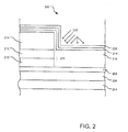
- Fig. 2 shows an intermediate step in the processing. While additional layers and features may also be included in the structure shown in Fig. 2, Fig. 2 shows an intermediate structure 200 that includes an antiferromagnetic
- a backfill layer 216 is shown above a portion of the barrier layer and extends along the layers of the free layer 210, cap layer 212, and photoresist layer 214.
- the field deposition of the backfill layer is shown in Fig. 2 as being thicker than the sidewall deposition along the free layer 210, cap layer 212, and photoresist layer 214.
- a material which will be referred to herein as a chemical-mechanical-polishing stop material (sometimes referred to as a CMP-stop) is shown as layer 218.
- a layer which will be referred to herein as a sacrificial layer is shown as layer 220.
- a "knock-off" procedure can be used to remove the material along the sidewall of the photoresist layer. This is shown in Fig. 2 by arrows 222 which are used to represent a removal operation, such as a milling operation. Because the thickness of the materials along the sidewall of the photoresist 214 is thicker than along the field of the areas, the removal operation exposes the sidewall of the photoresist layer without necessarily removing the field areas. The sacrificial layer protects the field portion of the CMP-stop material from being milled away. Thus, the full thickness of the CMP-stop material is retained for use during a subsequent CMP process.
- Fig. 3 shows a view of the intermediate structure after a milling procedure has taken place, for example.
- layers 204, 206, 208, 210, 212, 214, 216, and 218 are shown intact.
- Layer 220 has been slightly decreased in size due to the milling procedure.
- the modified version of layer 220 is shown as layer 221 in Fig. 3 .
- a "window" has been opened up in the layers that cover photoresist layer 214. This exposed area of the photoresist allows the photoresist removal solution to reach the photoresist layer during processing. The photoresist may then be easily removed.
- Fig. 4 shows the intermediate structure after removal of the photoresist. With the photoresist removed, a cap layer 212 is exposed.
- a structural remnant 222 of backfill material that was not previously milled away from the sidewall of the photoresist is left in place.
- the backfill remnant 222 was not removed by the milling process because of the backfill remnant's position at the base of the photoresist sidewall.
- the milling operation could not effectively remove the remnant at the same rate that other parts of the material along the sidewall of the photoresist were removed.
- Structural remnants such as the backfill remnant 222 could potentially interfere with the operation of the device being fabricated. For example, a remnant might affect the magnetic properties of a device. As a result, the remnant can be removed as shown in more detail below.
- Fig. 4 shows that the remnant 222 is shown adjacent a cap layer 212, a sacrificial layer 221, and a CMP-stop layer 218.
- a material such as alumina (Al 2 O 3 ) can be used for the backfill layer 216.
- These different materials can have different rates of responding to a CMP process.
- the cap layer shown in Fig. 4 can be quite hard so that it responds at a slow rate to a CMP process relative to a selected reference point or selected reference material.
- the backfill layer 216 (and remnant 222) can be made from a softer material such that layer 216 responds at a fast rate to a CMP process relative to a selected reference.
- the layer 218 which has been referred to as a CMP-stop layer can be selected to have a slow CMP rate.
- layer 218 has a CMP rate that is slow relative to a selected reference.
- the sacrificial layer 221 can have a fast CMP rate relative to a selected reference.
- the different CMP rate materials assist in polishing away the remnant 222 while achieving an end result that is substantially planar, as shown in Fig. 5 .
- the sacrificial material layer 221 has a fast CMP rate -- so, it is removed quite quickly.
- the remnant 222 is made from the backfill material -- so, it is also removed quite quickly.
- the cap material has a slow CMP rate -- so, it is not removed quickly.
- the CMP stop layer 218 has a slow CMP rate -- so, it is also not removed quickly.
- the CMP stop layer 218 protects the field area of the backfill layer 216, since the backfill layer has a high CMP rate.
- CMP process can remove the remnant feature 222 quickly while the cap layer 212 and CMP stop layer are more slowly reduced.
- the thickness of the CMP stop layer and sacrificial layer can be selected so that the CMP process exposes the field portion of the backfill layer 216 at the same time that the remnant 222 has been polished down to the field level of the backfill layer.
- a CMP stop layer thickness of about 1.0-5.0 nm could be utilized in one example.
- CMP stop materials can include, for example, Ir, Pt, Mo, Ti, W, and Ru, among others.
- a sacrificial layer thickness of about 1.0-5.0 nm could be used. Sacrificial materials can include for example Ni, NiFe, and Ta, among others.
- Fig. 5 shows an example of an intermediate structure after a CMP process has been performed.
- the cap layer 212 and the backfill layer 216 are shown in substantial alignment with one another.
- the edge formed by the back portion of cap layer 212 and free layer 210 and backfill layer 216 is substantially linear.
- a substantially linear edge for long SAF readers, for example, is believed to be difficult to achieve.
- the process described by using the process shown in Figs. 2-6 allows such a substantially linear edge for a long SAF reader to be achieved.
- a shield layer 224 is shown deposited over cap layer 212 and backfill layer 216.
- the cap layer and backfill layer are shown forming a substantially linear edge with the previous remnant removed.
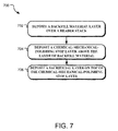
- Fig. 7 illustrates a flow chart of an example of a process 700 for preparing an intermediate structure for chemical-mechanical-polishing in accordance with certain embodiments.
- a layer of backfill material is deposited over a reader stack.
- a chemical-mechanical-polishing stop layer is deposited above the layer of backfill material in operation block 704.
- a sacrificial layer is deposited on top of the chemical-mechanical-polishing stop layer.
- Fig. 8 illustrates yet another example process via flow chart 800.
- an intermediate structure to be operated on is provided.
- a magnetic layer such as an SAF layer is disposed in proximity to the free layer.
- a portion of the free layer of the intermediate structure is removed while a corresponding portion of the SAF magnetic layer in proximity to the magnetic layer is not removed. This forms what is referred to as a long SAF read head because the SAF layer is substantially longer than the free layer.
- Operation block 804 notes that the process allows a substantially linear back edge to be formed by the reader stack.
- Fig. 2 shows substantially linear back edge 226. This substantially linear back edge is sometimes used to refer to the reader stack as being substantially vertical.
- a backfill material is deposited over a reader stack.
- Al 2 O 3 can be utilized as the backfill material.
- Other backfill materials may be utilized as well.
- a chemical-mechanical-polishing stop layer is deposited above the layer of backfill material in accordance with operation block 808.
- the CMP-stop layer is selected to have a CMP rate that is slower than the CMP rate of the backfill material.
- a sacrificial layer is deposited on top of the CMP-stop layer, as shown by block 810.
- the material used for the sacrificial layer can be selected to have a CMP rate that is faster than the CMP rate of the CMP-stop layer, for example.
- a portion of the photoresist layer that is disposed on the reader stack is exposed. For example, a portion of the material along the sidewall of the photoresist may be removed by a milling operation. Once the photoresist is exposed, the photoresist is removed, as shown by operation block 814. Operation block 816 shows that a cap on the reader can have a thickness of approximately 0.5 to 5.0 nanometers, depending on the desired design.
- the processes and structures described above can be beneficial for different reasons.
- the process described herein allows a long SAF reader to be formed.
- a long SAF reader with a substantially vertical back edge can be formed.
- Another way to state this is that the back edge of the read stack and the backfill layer can form an angle of approximately 90 degrees.
- a thin cap layer over a reader stack may be formed.
- the thin cap layer can be formed consistently from wafer to wafer by the process described herein because the CMP process can be controlled.
- the "knock-off" process described herein allows a thin cap layer to be used over the reader stack while a thin cap has been more difficult to implement with a process often referred to as a photoresist "lift-off" process.
Landscapes
- Engineering & Computer Science (AREA)
- Manufacturing & Machinery (AREA)
- Mechanical Engineering (AREA)
- Magnetic Heads (AREA)
- Finish Polishing, Edge Sharpening, And Grinding By Specific Grinding Devices (AREA)
- Hall/Mr Elements (AREA)
- Mechanical Treatment Of Semiconductor (AREA)
Abstract
Description
- In semiconductor manufacturing, even small topological structures can impact the performance of a device. For example, in devices using magnetic materials, small topological structures can impact the magnetic properties of the device. As one example, a read head used in disc drives can be fabricated using semiconductor processing. The read head can utilize several different layers of materials in order to form a reader stack (or read sensor) in the desired configuration. A reader stack is the portion of read head that is configured to sense changes in a magnetic field. Thus, during operation, the reader stack can sense a change in the magnetic field of a magnetic medium positioned proximate to the reader stack. If a topological remnant is left behind from processing steps used to fabricate the read head, that topological remnant can potentially impact the magnetic properties of the read head depending on the size, location, and material of the topological remnant.
- This Summary is provided to introduce a selection of concepts in a simplified form that are further described below in the Detailed Description. This Summary is not intended to identify key features or essential features of the claimed subject matter, nor is it intended to be used to limit the scope of the claimed subject matter. Other features, details, utilities, and advantages of the claimed subject matter will be apparent from the following more particular written Detailed Description of various implementations and implementations as further illustrated in the accompanying drawings and defined in the appended claims.
- In accordance with certain embodiments, an apparatus includes a reader stack; a backfill layer disposed next to the reader stack; a chemical-mechanical polishing stop layer disposed above the backfill layer; and a sacrificial layer disposed on top of the chemical-mechanical-polishing stop layer.
- In accordance with certain embodiments, a method can be utilized that includes depositing a backfill material layer over a reader stack; depositing a chemical-mechanical-polishing stop layer above the layer of backfill material; and depositing a sacrificial layer on top of the chemical-mechanical-polishing stop layer.
- These and various other features will be apparent from the following detailed description.
- Embodiments of the present invention will now be described by way of further example only and with reference to the accompanying drawings, in which:
-
Fig. 1 illustrates an example block diagram for a disc drive system with an enlarged view of a cross-section of a long SAF read head having a substantially linear back edge, in accordance with certain embodiments. -
Fig. 2 illustrates a cross-sectional view of removing backfill material during processing of a long SAF read head, in accordance with certain embodiments. -
Fig. 3 illustrates a cross-sectional view during the processing of a long SAF read head wherein backfill material has been removed to expose the side of photoresist, in accordance with certain embodiments. -
Fig. 4 illustrates a cross-sectional view during processing of a long SAF read head wherein photoresist has been removed to expose a backfill topographical remnant, in accordance with certain embodiments. -
Fig. 5 illustrates a cross-sectional view during processing of a long SAF read head wherein a backfill remnant has been removed, in accordance with certain embodiments. -
Fig. 6 illustrates a cross-sectional view during processing of a long SAF read head wherein a shield layer has been formed over the substantially planar backfill layer, in accordance with certain embodiments. -
Fig. 7 illustrates a flow chart that shows a method of preparing an intermediate structure for chemical-mechanical-polishing in accordance with certain embodiments. -
Fig. 8 illustrates yet another flow chart that shows a method of preparing an intermediate structure for chemical-mechanical-polishing in accordance with certain embodiments. - Embodiments of the present technology are disclosed herein in the context of a read head for use with a disc drive system. However, it should be understood that the technology is not limited to a read head for a disc drive system and could readily be applied to other technology systems as well.
- With reference now to
FIG. 1 , an example of a disc drive system in accordance with one embodiment is shown. A disc drive system is but one example where the disclosed technology may be utilized.FIG. 1 illustrates aperspective view 100 of an example disc drive system. Adisc 102 rotates about a spindle center or a disc axis ofrotation 104 during operation. Thedisc 102 includes aninner diameter 106 and anouter diameter 108 between which are a number ofconcentric data tracks 110. Thedata tracks 110 are substantially circular. It should be understood, however, that the described technology may be employed with other types of storage media. - Information may be written to and read from the
different data tracks 110. Atransducer head 124 is mounted on anactuator assembly 120 at an end distal to an actuator axis ofrotation 122 and thetransducer head 124 flies in close proximity above the surface of thedisc 102 during disc operation. Theactuator assembly 120 rotates during a seek operation about the actuator axis ofrotation 122 positioned adjacent to thedisc 102. The seek operation positions thetransducer head 124 over a target data track of thedata tracks 110. - The exploded
view 140 shows a cross-sectional view of a portion of a transducer head that is utilizing a long SAF read head. A read head formed with an SAF layer that is much longer than the associated free layer is referred to as a "long SAF read head." The cross-sectional view shows ashield layer 224, acap layer 212, afree layer 210, abarrier layer 208, along SAF layer 206, and anantiferromagnetic layer 204. Additional layers are not shown. The long SAF read head is shown with a substantiallylinear back edge 226. A substantially linear back edge is believed to be difficult to achieve for a long SAF read head. In accordance with certain embodiments, a process for forming a long SAF read head with a substantially linear back edge is described in further detail below. - Referring now to
Figs. 2-6 , a process for forming a long SAF read head is disclosed in accordance with certain embodiments.Fig. 2 shows an intermediate step in the processing. While additional layers and features may also be included in the structure shown inFig. 2, Fig. 2 shows anintermediate structure 200 that includes an antiferromagnetic - (AFM)
layer 204, a synthetic antiferromagnetic (SAF)layer 206, abarrier layer 208, afree layer 210, acap layer 212, aphotoresist layer 214. Abackfill layer 216 is shown above a portion of the barrier layer and extends along the layers of thefree layer 210,cap layer 212, andphotoresist layer 214. The field deposition of the backfill layer is shown inFig. 2 as being thicker than the sidewall deposition along thefree layer 210,cap layer 212, andphotoresist layer 214. A material which will be referred to herein as a chemical-mechanical-polishing stop material (sometimes referred to as a CMP-stop) is shown aslayer 218. And, a layer which will be referred to herein as a sacrificial layer is shown aslayer 220. - In order to remove the
photoresist layer 214, the photoresist is exposed to a solution that can be used to remove the photoresist from thestructure 200.Fig. 2 shows the photoresist as being covered by other layers and therefore not readily accessible to the photoresist removal solution. Therefore, in accordance with certain embodiments a "knock-off" procedure can be used to remove the material along the sidewall of the photoresist layer. This is shown inFig. 2 byarrows 222 which are used to represent a removal operation, such as a milling operation. Because the thickness of the materials along the sidewall of thephotoresist 214 is thicker than along the field of the areas, the removal operation exposes the sidewall of the photoresist layer without necessarily removing the field areas. The sacrificial layer protects the field portion of the CMP-stop material from being milled away. Thus, the full thickness of the CMP-stop material is retained for use during a subsequent CMP process. - Thus,
Fig. 3 shows a view of the intermediate structure after a milling procedure has taken place, for example. InFig. 3 ,layers Layer 220 has been slightly decreased in size due to the milling procedure. The modified version oflayer 220 is shown aslayer 221 inFig. 3 . As can be seen inFig. 3 , a "window" has been opened up in the layers that coverphotoresist layer 214. This exposed area of the photoresist allows the photoresist removal solution to reach the photoresist layer during processing. The photoresist may then be easily removed. -
Fig. 4 shows the intermediate structure after removal of the photoresist. With the photoresist removed, acap layer 212 is exposed. One interesting feature of this process is that astructural remnant 222 of backfill material that was not previously milled away from the sidewall of the photoresist is left in place. Thebackfill remnant 222 was not removed by the milling process because of the backfill remnant's position at the base of the photoresist sidewall. The milling operation could not effectively remove the remnant at the same rate that other parts of the material along the sidewall of the photoresist were removed. Structural remnants such as thebackfill remnant 222 could potentially interfere with the operation of the device being fabricated. For example, a remnant might affect the magnetic properties of a device. As a result, the remnant can be removed as shown in more detail below. -
Fig. 4 shows that the remnant 222 is shown adjacent acap layer 212, asacrificial layer 221, and a CMP-stop layer 218. In certain embodiments, a material such as alumina (Al2O3) can be used for thebackfill layer 216. These different materials can have different rates of responding to a CMP process. For example, the cap layer shown inFig. 4 can be quite hard so that it responds at a slow rate to a CMP process relative to a selected reference point or selected reference material. The backfill layer 216 (and remnant 222) can be made from a softer material such thatlayer 216 responds at a fast rate to a CMP process relative to a selected reference. Thelayer 218 which has been referred to as a CMP-stop layer can be selected to have a slow CMP rate. Thus,layer 218 has a CMP rate that is slow relative to a selected reference. And, thesacrificial layer 221 can have a fast CMP rate relative to a selected reference. - When a chemical-mechanical-polishing procedure is performed on the intermediate structure shown in
Fig. 4 , the different CMP rate materials assist in polishing away the remnant 222 while achieving an end result that is substantially planar, as shown inFig. 5 . Thesacrificial material layer 221 has a fast CMP rate -- so, it is removed quite quickly. Similarly, the remnant 222 is made from the backfill material -- so, it is also removed quite quickly. The cap material has a slow CMP rate -- so, it is not removed quickly. TheCMP stop layer 218 has a slow CMP rate -- so, it is also not removed quickly. TheCMP stop layer 218 protects the field area of thebackfill layer 216, since the backfill layer has a high CMP rate. As a result, CMP process can remove theremnant feature 222 quickly while thecap layer 212 and CMP stop layer are more slowly reduced. The thickness of the CMP stop layer and sacrificial layer can be selected so that the CMP process exposes the field portion of thebackfill layer 216 at the same time that the remnant 222 has been polished down to the field level of the backfill layer. For example, a CMP stop layer thickness of about 1.0-5.0 nm could be utilized in one example. CMP stop materials can include, for example, Ir, Pt, Mo, Ti, W, and Ru, among others. And, a sacrificial layer thickness of about 1.0-5.0 nm could be used. Sacrificial materials can include for example Ni, NiFe, and Ta, among others. -
Fig. 5 shows an example of an intermediate structure after a CMP process has been performed. Thecap layer 212 and thebackfill layer 216 are shown in substantial alignment with one another. Also, the edge formed by the back portion ofcap layer 212 andfree layer 210 andbackfill layer 216 is substantially linear. A substantially linear edge for long SAF readers, for example, is believed to be difficult to achieve. The process described by using the process shown inFigs. 2-6 allows such a substantially linear edge for a long SAF reader to be achieved. - Referring now to
Fig. 6 , ashield layer 224 is shown deposited overcap layer 212 andbackfill layer 216. The cap layer and backfill layer are shown forming a substantially linear edge with the previous remnant removed. -
Fig. 7 illustrates a flow chart of an example of aprocess 700 for preparing an intermediate structure for chemical-mechanical-polishing in accordance with certain embodiments. In operation 702 ofFig. 7 , a layer of backfill material is deposited over a reader stack. A chemical-mechanical-polishing stop layer is deposited above the layer of backfill material inoperation block 704. Inoperation block 706, a sacrificial layer is deposited on top of the chemical-mechanical-polishing stop layer. -
Fig. 8 illustrates yet another example process viaflow chart 800. Inblock 802, an intermediate structure to be operated on is provided. A magnetic layer such as an SAF layer is disposed in proximity to the free layer. A portion of the free layer of the intermediate structure is removed while a corresponding portion of the SAF magnetic layer in proximity to the magnetic layer is not removed. This forms what is referred to as a long SAF read head because the SAF layer is substantially longer than the free layer. - Operation block 804 notes that the process allows a substantially linear back edge to be formed by the reader stack. For example,
Fig. 2 shows substantiallylinear back edge 226. This substantially linear back edge is sometimes used to refer to the reader stack as being substantially vertical. - In
operation block 806, a backfill material is deposited over a reader stack. For example, Al2O3 can be utilized as the backfill material. Other backfill materials may be utilized as well. A chemical-mechanical-polishing stop layer is deposited above the layer of backfill material in accordance withoperation block 808. The CMP-stop layer is selected to have a CMP rate that is slower than the CMP rate of the backfill material. In addition, a sacrificial layer is deposited on top of the CMP-stop layer, as shown byblock 810. The material used for the sacrificial layer can be selected to have a CMP rate that is faster than the CMP rate of the CMP-stop layer, for example. - In operation block 812, a portion of the photoresist layer that is disposed on the reader stack is exposed. For example, a portion of the material along the sidewall of the photoresist may be removed by a milling operation. Once the photoresist is exposed, the photoresist is removed, as shown by
operation block 814. Operation block 816 shows that a cap on the reader can have a thickness of approximately 0.5 to 5.0 nanometers, depending on the desired design. - The processes and structures described above can be beneficial for different reasons. For example, the process described herein allows a long SAF reader to be formed. Moreover, in accordance with certain embodiments, a long SAF reader with a substantially vertical back edge can be formed. Another way to state this is that the back edge of the read stack and the backfill layer can form an angle of approximately 90 degrees.
- In certain embodiments, a thin cap layer over a reader stack may be formed. The thin cap layer can be formed consistently from wafer to wafer by the process described herein because the CMP process can be controlled. The "knock-off" process described herein allows a thin cap layer to be used over the reader stack while a thin cap has been more difficult to implement with a process often referred to as a photoresist "lift-off" process.
- It is noted that many of the structures, materials, and acts recited herein can be recited as means for performing a function or step for performing a function. Therefore, it should be understood that such language is entitled to cover all such structures, materials, or acts disclosed within this specification and any modifications falling within the scope of the claims.
- It is thought that the apparatuses and methods of embodiments described herein will be understood from this specification. While the above description is a complete description of specific embodiments, the above description should not be taken as limiting the scope of the patent as defined by the claims.
Claims (20)
- A method comprising:(702) depositing a backfill material layer (216) over a reader stack;(704) depositing a chemical-mechanical-polishing stop layer (218) above the layer of backfill material;(708) depositing a sacrificial layer (220) on top of the chemical-mechanical-polishing stop layer.
- The method as claimed in claim 1 and further comprising:(810) exposing a portion of a photoresist layer (214) disposed on the reader stack.
- The method as claimed in claim 2 and further comprising:(814) removing the photoresist (214) via the exposed portion.
- The method as claimed in claim 2 or claim 3 wherein the exposing the portion of the photoresist layer comprises:milling through the sacrificial layer (220), the chemical-mechanical-polishing stop layer (218), and the backfill layer (216).
- The method as claimed in any one of the preceding claims and further comprising:(804) forming a substantially vertical reader stack.
- The method as claimed in any one of the preceding claims and further comprising:(814) removing a portion of a free layer (210) while not removing a corresponding portion of a magnetic layer disposed beneath the free layer so as to form a long stripe magnetic reader.
- The method as claimed in any one of the preceding claims and further comprising:utilizing Al2O3 as the backfill layer (216).
- The method as claimed in any one of the preceding claims and further comprising:(816) forming a cap (212) on the reader having a thickness between about 0.5 nm and about 5.0 nm.
- The method as claimed in any one of the preceding claims wherein the sacrificial layer (220) has a first CMP rate and the chemical-mechanical-polishing stop layer (218) has a second CMP rate and wherein the first CMP rate is greater than the second CMP rate.
- The method as claimed in claim 9 wherein the backfill layer (216) has a third CMP rate and wherein the third CMP rate is greater than the second CMP rate.
- An apparatus comprising:a reader stack;a backfill layer (216) disposed next to the reader stack;a chemical-mechanical polishing stop layer (218) disposed above the backfill layer;a sacrificial layer (220) disposed on top of the chemical-mechanical-polishing stop layer.
- The apparatus as claimed in claim 11 and further comprising:a photoresist layer (214) disposed on top of the reader stack; andwherein the backfill layer (216) covers the photoresist layer.
- The apparatus as claimed in claim 12 and further comprising:an opening formed in the backfill layer (216) so as to expose the photoresist layer (214).
- The apparatus as claimed in claim 13 wherein the opening is an opening formed by milling.
- The apparatus as claimed in any one of claims 11 to 14 wherein the reader stack comprises substantially vertical sidewalls.
- The apparatus as claimed in any one of claims 11 to 15 and further comprising:a free layer (210);a magnetic layer disposed beneath the free layer and having a length longer than the length of the free layer.
- The apparatus as claimed in any one of claims 11 to 16 wherein the backfill layer comprises Al2O3.
- The apparatus as claimed in any one of claims 11 to 17 and further comprising:a cap layer (212) on the reader stack comprising a thickness between about 0.5 nm and about 5.0 nm.
- The apparatus as claimed in any one of claims 11 to 18 wherein the sacrificial layer (220) has a first CMP rate and the chemical-mechanical-polishing stop layer (218) has a second CMP rate and wherein the first CMP rate is greater than the second CMP rate.
- The apparatus as claimed in claim 19 wherein the backfill layer (216) has a third CMP rate and wherein the third CMP rate is greater than the second CMP rate.
Applications Claiming Priority (1)
| Application Number | Priority Date | Filing Date | Title |
|---|---|---|---|
| US13/797,381 US8947834B2 (en) | 2013-03-12 | 2013-03-12 | Method and apparatus for chemical-mechanical polishing |
Publications (2)
| Publication Number | Publication Date |
|---|---|
| EP2779168A2 true EP2779168A2 (en) | 2014-09-17 |
| EP2779168A3 EP2779168A3 (en) | 2015-03-11 |
Family
ID=50276961
Family Applications (1)
| Application Number | Title | Priority Date | Filing Date |
|---|---|---|---|
| EP14159077.8A Withdrawn EP2779168A3 (en) | 2013-03-12 | 2014-03-12 | Method and apparatus for chemical-mechanical polishing |
Country Status (5)
| Country | Link |
|---|---|
| US (1) | US8947834B2 (en) |
| EP (1) | EP2779168A3 (en) |
| JP (1) | JP6215739B2 (en) |
| KR (1) | KR101750736B1 (en) |
| CN (1) | CN104050976B (en) |
Families Citing this family (1)
| Publication number | Priority date | Publication date | Assignee | Title |
|---|---|---|---|---|
| US8771847B2 (en) * | 2011-10-14 | 2014-07-08 | Seagate Technology | Reader stop-layers |
Family Cites Families (22)
| Publication number | Priority date | Publication date | Assignee | Title |
|---|---|---|---|---|
| US6743642B2 (en) * | 2002-11-06 | 2004-06-01 | International Business Machines Corporation | Bilayer CMP process to improve surface roughness of magnetic stack in MRAM technology |
| US7587810B2 (en) * | 2004-04-30 | 2009-09-15 | Hitachi Global Storage Technologies Netherlands B.V. | High milling resistance write pole fabrication method for perpendicular recording |
| US7340824B2 (en) * | 2004-06-30 | 2008-03-11 | Hitachi Global Storage Technologies Netherlands B.V. | Method for fabricating a magnetic head having an improved magnetic shield |
| US7765676B2 (en) * | 2004-11-18 | 2010-08-03 | Hitachi Global Storage Technologies Netherlands B.V. | Method for patterning a magnetoresistive sensor |
| JP2006179051A (en) * | 2004-12-21 | 2006-07-06 | Hitachi Global Storage Technologies Netherlands Bv | Magnetoresistive sensor and its manufacturing method |
| US7663846B2 (en) * | 2005-12-07 | 2010-02-16 | Hitachi Global Storage Technologies Netherlands B. V. | Magnetoresistive sensor having an enhanced lead overlay design and shape enhanced pinning |
| US7522391B2 (en) * | 2005-12-14 | 2009-04-21 | Hitachi Global Storage Technologies Netherlands B.V. | Current perpendicular to plane magnetoresistive sensor having a shape enhanced pinned layer and an in stack bias structure |
| US7843665B2 (en) * | 2006-09-11 | 2010-11-30 | Headway Technologies, Inc. | Perpendicular magnetic recording head with nonmagnetic metal layer even with top face of pole layer |
| US8634162B2 (en) * | 2007-03-08 | 2014-01-21 | HGST Netherlands B.V. | Perpendicular write head having a stepped flare structure and method of manufacture thereof |
| US7950137B2 (en) * | 2007-06-21 | 2011-05-31 | Hitachi Global Storage Technologies Netherlands B.V. | Method for manufacturing a magnetic write head |
| US7788798B2 (en) * | 2007-11-21 | 2010-09-07 | Hitachi Global Storage Technologies Netherlands B.V. | Method for manufacturing a perpendicular magnetic write head with wrap around magnetic trailing and side shields |
| US8316527B2 (en) * | 2008-04-01 | 2012-11-27 | Western Digital (Fremont), Llc | Method for providing at least one magnetoresistive device |
| US20090266790A1 (en) * | 2008-04-28 | 2009-10-29 | Hamid Balamane | Method of making a magnetoresistive reader structure |
| US8136226B2 (en) * | 2008-05-16 | 2012-03-20 | Hitachi Global Storage Technologies Netherlands B.V. | Read sensors and methods of making same with back-edge milling and refilling |
| US8349195B1 (en) * | 2008-06-27 | 2013-01-08 | Western Digital (Fremont), Llc | Method and system for providing a magnetoresistive structure using undercut free mask |
| US8225487B2 (en) * | 2008-07-25 | 2012-07-24 | Hitachi Global Storage Technologies Netherlands B.V. | Method for confining sense current of a read transducer to an air-bearing surface(ABS) side of a free layer |
| US8011084B2 (en) * | 2008-07-31 | 2011-09-06 | Hitachi Global Storage Technologies Netherlands B.V. | Method for fabricating narrow magnetic read width TMR/CPP sensors |
| US8268407B2 (en) * | 2008-09-08 | 2012-09-18 | Hitachi Global Storage Technologies Netherlands B.V. | Method for manufacturing a perpendicular magnetic write head having write pole |
| US8066893B2 (en) * | 2008-12-23 | 2011-11-29 | Hitachi Global Storage Technologies Netherlands B.V. | Method for creating a magnetic write pole having a stepped perpendicular pole via CMP-assisted liftoff |
| US8441757B2 (en) * | 2009-12-09 | 2013-05-14 | HGST Netherlands B.V. | Perpendicular magnetic write head with wrap-around shield, slanted pole and slanted pole bump fabricated by damascene process |
| US8347489B2 (en) * | 2010-09-01 | 2013-01-08 | Hitachi Global Storage Technologies Netherlands B.V. | Method for manufacturing a perpendicular magnetic write head having a leading edge tapered write pole, self aligned side shield and independent trailing shield |
| US20120231296A1 (en) * | 2011-03-11 | 2012-09-13 | Hitachi Global Storage Technologies Netherlands B.V. | Method for manufacturing an advanced magnetic read sensor |
-
2013
- 2013-03-12 US US13/797,381 patent/US8947834B2/en active Active
-
2014
- 2014-03-06 KR KR1020140026625A patent/KR101750736B1/en not_active Expired - Fee Related
- 2014-03-11 JP JP2014047701A patent/JP6215739B2/en not_active Expired - Fee Related
- 2014-03-11 CN CN201410087533.8A patent/CN104050976B/en not_active Expired - Fee Related
- 2014-03-12 EP EP14159077.8A patent/EP2779168A3/en not_active Withdrawn
Non-Patent Citations (1)
| Title |
|---|
| None |
Also Published As
| Publication number | Publication date |
|---|---|
| US20140272472A1 (en) | 2014-09-18 |
| CN104050976B (en) | 2018-06-05 |
| JP6215739B2 (en) | 2017-10-18 |
| EP2779168A3 (en) | 2015-03-11 |
| CN104050976A (en) | 2014-09-17 |
| JP2014175049A (en) | 2014-09-22 |
| KR101750736B1 (en) | 2017-06-27 |
| US8947834B2 (en) | 2015-02-03 |
| KR20140111961A (en) | 2014-09-22 |
Similar Documents
| Publication | Publication Date | Title |
|---|---|---|
| US8617408B2 (en) | Method for manufacturing a magnetic read sensor with narrow track width using amorphous carbon as a hard mask and localized CMP | |
| KR101621364B1 (en) | Multi-reader method and apparatus | |
| US20100024201A1 (en) | Method for fabricating narrow magnetic read width tmr/cpp sensors | |
| US20070081279A1 (en) | Double mill process for patterning current perpendicular to plane (CPP) magnetoresistive devices to minimize barrier shorting and barrier damage | |
| US8393073B2 (en) | Method to control mask profile for read sensor definition | |
| US20090266790A1 (en) | Method of making a magnetoresistive reader structure | |
| US20140168824A1 (en) | Magnetic sensor having an extended pinned layer and shape enhanced bias structure | |
| US8296930B2 (en) | Method for manufacturing a magnetoresistive sensor having a flat shield | |
| US20120187079A1 (en) | Method for manufacturing a magnetic sensor having a flat upper shield | |
| US7248434B2 (en) | Planarized perpendicular pole tip system and method for manufacturing the same | |
| EP1752781A2 (en) | Magnetoresistive sensor having an anistropic pinned layer for pinning improvement | |
| US8947834B2 (en) | Method and apparatus for chemical-mechanical polishing | |
| JP2015146224A (en) | Magnetic sensor with narrow track width and small read gap | |
| US7324311B2 (en) | Rie defined CPP read heads | |
| US9105295B2 (en) | Pattern tone reversal | |
| US9030786B2 (en) | Magnetic head having a soft magnetic layer with a close-packed plane thereof being parallel or oblique to an air bearing surface | |
| US20120231296A1 (en) | Method for manufacturing an advanced magnetic read sensor | |
| US8780499B2 (en) | Magnetic write head having a residual shield seed layer for reducing overwriting | |
| US8225487B2 (en) | Method for confining sense current of a read transducer to an air-bearing surface(ABS) side of a free layer | |
| US9373344B2 (en) | Two side by side MIMO read sensors fabricated by self-aligned processing | |
| US9406323B2 (en) | Slider with aluminum compound fill | |
| US7768748B2 (en) | Magnetoresistive sensor with overlaid combined leads and shields | |
| US8801943B2 (en) | Method for manufacturing wraparound shield write head using hard masks | |
| US20070236832A1 (en) | Lift-off method for forming write pole of a magnetic write head and write pole formed thereby |
Legal Events
| Date | Code | Title | Description |
|---|---|---|---|
| 17P | Request for examination filed |
Effective date: 20140331 |
|
| AK | Designated contracting states |
Kind code of ref document: A2 Designated state(s): AL AT BE BG CH CY CZ DE DK EE ES FI FR GB GR HR HU IE IS IT LI LT LU LV MC MK MT NL NO PL PT RO RS SE SI SK SM TR |
|
| AX | Request for extension of the european patent |
Extension state: BA ME |
|
| PUAI | Public reference made under article 153(3) epc to a published international application that has entered the european phase |
Free format text: ORIGINAL CODE: 0009012 |
|
| PUAL | Search report despatched |
Free format text: ORIGINAL CODE: 0009013 |
|
| AK | Designated contracting states |
Kind code of ref document: A3 Designated state(s): AL AT BE BG CH CY CZ DE DK EE ES FI FR GB GR HR HU IE IS IT LI LT LU LV MC MK MT NL NO PL PT RO RS SE SI SK SM TR |
|
| AX | Request for extension of the european patent |
Extension state: BA ME |
|
| RIC1 | Information provided on ipc code assigned before grant |
Ipc: G11B 5/39 20060101AFI20150203BHEP Ipc: G11B 5/31 20060101ALI20150203BHEP |
|
| RBV | Designated contracting states (corrected) |
Designated state(s): AL AT BE BG CH CY CZ DE DK EE ES FI FR GB GR HR HU IE IS IT LI LT LU LV MC MK MT NL NO PL PT RO RS SE SI SK SM TR |
|
| 17Q | First examination report despatched |
Effective date: 20190227 |
|
| STAA | Information on the status of an ep patent application or granted ep patent |
Free format text: STATUS: THE APPLICATION IS DEEMED TO BE WITHDRAWN |
|
| 18D | Application deemed to be withdrawn |
Effective date: 20190710 |