EP2779167A2 - Bottom shield stabilized magnetic seed layer - Google Patents
Bottom shield stabilized magnetic seed layer Download PDFInfo
- Publication number
- EP2779167A2 EP2779167A2 EP20140160342 EP14160342A EP2779167A2 EP 2779167 A2 EP2779167 A2 EP 2779167A2 EP 20140160342 EP20140160342 EP 20140160342 EP 14160342 A EP14160342 A EP 14160342A EP 2779167 A2 EP2779167 A2 EP 2779167A2
- Authority
- EP
- European Patent Office
- Prior art keywords
- magnetic
- shield
- stack
- bottom shield
- magnetic stack
- Prior art date
- Legal status (The legal status is an assumption and is not a legal conclusion. Google has not performed a legal analysis and makes no representation as to the accuracy of the status listed.)
- Ceased
Links
- 230000005291 magnetic effect Effects 0.000 title claims abstract description 159
- 230000005415 magnetization Effects 0.000 claims abstract description 66
- 238000000137 annealing Methods 0.000 claims description 15
- 230000005294 ferromagnetic effect Effects 0.000 claims description 10
- 238000000034 method Methods 0.000 claims description 8
- 125000006850 spacer group Chemical group 0.000 claims description 4
- 239000010410 layer Substances 0.000 description 54
- 230000002463 transducing effect Effects 0.000 description 15
- 238000003475 lamination Methods 0.000 description 12
- 238000013500 data storage Methods 0.000 description 11
- 238000004519 manufacturing process Methods 0.000 description 6
- 230000033001 locomotion Effects 0.000 description 5
- 238000003860 storage Methods 0.000 description 5
- 230000008878 coupling Effects 0.000 description 4
- 238000010168 coupling process Methods 0.000 description 4
- 238000005859 coupling reaction Methods 0.000 description 4
- 239000000463 material Substances 0.000 description 4
- 230000004888 barrier function Effects 0.000 description 3
- 230000005381 magnetic domain Effects 0.000 description 3
- 230000006641 stabilisation Effects 0.000 description 3
- 238000011105 stabilization Methods 0.000 description 3
- PNEYBMLMFCGWSK-UHFFFAOYSA-N aluminium oxide Inorganic materials [O-2].[O-2].[O-2].[Al+3].[Al+3] PNEYBMLMFCGWSK-UHFFFAOYSA-N 0.000 description 2
- 238000010276 construction Methods 0.000 description 2
- 238000000151 deposition Methods 0.000 description 2
- 238000005516 engineering process Methods 0.000 description 2
- 239000000696 magnetic material Substances 0.000 description 2
- 230000035945 sensitivity Effects 0.000 description 2
- 230000000903 blocking effect Effects 0.000 description 1
- 229910052802 copper Inorganic materials 0.000 description 1
- 230000003247 decreasing effect Effects 0.000 description 1
- 230000000593 degrading effect Effects 0.000 description 1
- 230000008021 deposition Effects 0.000 description 1
- 238000005530 etching Methods 0.000 description 1
- 239000011810 insulating material Substances 0.000 description 1
- 239000012212 insulator Substances 0.000 description 1
- 230000002452 interceptive effect Effects 0.000 description 1
- 238000001459 lithography Methods 0.000 description 1
- 238000005259 measurement Methods 0.000 description 1
- 238000005457 optimization Methods 0.000 description 1
- 238000000059 patterning Methods 0.000 description 1
- 229910052709 silver Inorganic materials 0.000 description 1
- 239000002356 single layer Substances 0.000 description 1
- 238000004513 sizing Methods 0.000 description 1
- 230000000087 stabilizing effect Effects 0.000 description 1
- 239000000126 substance Substances 0.000 description 1
- 230000003746 surface roughness Effects 0.000 description 1
- 238000012876 topography Methods 0.000 description 1
Images

Classifications
-
- G—PHYSICS
- G11—INFORMATION STORAGE
- G11B—INFORMATION STORAGE BASED ON RELATIVE MOVEMENT BETWEEN RECORD CARRIER AND TRANSDUCER
- G11B5/00—Recording by magnetisation or demagnetisation of a record carrier; Reproducing by magnetic means; Record carriers therefor
- G11B5/127—Structure or manufacture of heads, e.g. inductive
- G11B5/31—Structure or manufacture of heads, e.g. inductive using thin films
- G11B5/3109—Details
- G11B5/3116—Shaping of layers, poles or gaps for improving the form of the electrical signal transduced, e.g. for shielding, contour effect, equalizing, side flux fringing, cross talk reduction between heads or between heads and information tracks
-
- G—PHYSICS
- G11—INFORMATION STORAGE
- G11B—INFORMATION STORAGE BASED ON RELATIVE MOVEMENT BETWEEN RECORD CARRIER AND TRANSDUCER
- G11B5/00—Recording by magnetisation or demagnetisation of a record carrier; Reproducing by magnetic means; Record carriers therefor
- G11B5/127—Structure or manufacture of heads, e.g. inductive
- G11B5/31—Structure or manufacture of heads, e.g. inductive using thin films
- G11B5/3163—Fabrication methods or processes specially adapted for a particular head structure, e.g. using base layers for electroplating, using functional layers for masking, using energy or particle beams for shaping the structure or modifying the properties of the basic layers
-
- G—PHYSICS
- G11—INFORMATION STORAGE
- G11B—INFORMATION STORAGE BASED ON RELATIVE MOVEMENT BETWEEN RECORD CARRIER AND TRANSDUCER
- G11B5/00—Recording by magnetisation or demagnetisation of a record carrier; Reproducing by magnetic means; Record carriers therefor
- G11B5/10—Structure or manufacture of housings or shields for heads
- G11B5/11—Shielding of head against electric or magnetic fields
- G11B5/115—Shielding devices arranged between heads or windings
-
- G—PHYSICS
- G11—INFORMATION STORAGE
- G11B—INFORMATION STORAGE BASED ON RELATIVE MOVEMENT BETWEEN RECORD CARRIER AND TRANSDUCER
- G11B5/00—Recording by magnetisation or demagnetisation of a record carrier; Reproducing by magnetic means; Record carriers therefor
- G11B5/127—Structure or manufacture of heads, e.g. inductive
- G11B5/33—Structure or manufacture of flux-sensitive heads, i.e. for reproduction only; Combination of such heads with means for recording or erasing only
- G11B5/39—Structure or manufacture of flux-sensitive heads, i.e. for reproduction only; Combination of such heads with means for recording or erasing only using magneto-resistive devices or effects
- G11B5/3903—Structure or manufacture of flux-sensitive heads, i.e. for reproduction only; Combination of such heads with means for recording or erasing only using magneto-resistive devices or effects using magnetic thin film layers or their effects, the films being part of integrated structures
- G11B5/3906—Details related to the use of magnetic thin film layers or to their effects
- G11B5/3912—Arrangements in which the active read-out elements are transducing in association with active magnetic shields, e.g. magnetically coupled shields
-
- G—PHYSICS
- G11—INFORMATION STORAGE
- G11B—INFORMATION STORAGE BASED ON RELATIVE MOVEMENT BETWEEN RECORD CARRIER AND TRANSDUCER
- G11B5/00—Recording by magnetisation or demagnetisation of a record carrier; Reproducing by magnetic means; Record carriers therefor
- G11B5/127—Structure or manufacture of heads, e.g. inductive
- G11B5/33—Structure or manufacture of flux-sensitive heads, i.e. for reproduction only; Combination of such heads with means for recording or erasing only
- G11B5/39—Structure or manufacture of flux-sensitive heads, i.e. for reproduction only; Combination of such heads with means for recording or erasing only using magneto-resistive devices or effects
- G11B5/3903—Structure or manufacture of flux-sensitive heads, i.e. for reproduction only; Combination of such heads with means for recording or erasing only using magneto-resistive devices or effects using magnetic thin film layers or their effects, the films being part of integrated structures
- G11B5/398—Specially shaped layers
-
- G—PHYSICS
- G11—INFORMATION STORAGE
- G11B—INFORMATION STORAGE BASED ON RELATIVE MOVEMENT BETWEEN RECORD CARRIER AND TRANSDUCER
- G11B5/00—Recording by magnetisation or demagnetisation of a record carrier; Reproducing by magnetic means; Record carriers therefor
- G11B5/127—Structure or manufacture of heads, e.g. inductive
- G11B5/33—Structure or manufacture of flux-sensitive heads, i.e. for reproduction only; Combination of such heads with means for recording or erasing only
- G11B5/39—Structure or manufacture of flux-sensitive heads, i.e. for reproduction only; Combination of such heads with means for recording or erasing only using magneto-resistive devices or effects
- G11B2005/3996—Structure or manufacture of flux-sensitive heads, i.e. for reproduction only; Combination of such heads with means for recording or erasing only using magneto-resistive devices or effects large or giant magnetoresistive effects [GMR], e.g. as generated in spin-valve [SV] devices
-
- Y—GENERAL TAGGING OF NEW TECHNOLOGICAL DEVELOPMENTS; GENERAL TAGGING OF CROSS-SECTIONAL TECHNOLOGIES SPANNING OVER SEVERAL SECTIONS OF THE IPC; TECHNICAL SUBJECTS COVERED BY FORMER USPC CROSS-REFERENCE ART COLLECTIONS [XRACs] AND DIGESTS
- Y10—TECHNICAL SUBJECTS COVERED BY FORMER USPC
- Y10T—TECHNICAL SUBJECTS COVERED BY FORMER US CLASSIFICATION
- Y10T156/00—Adhesive bonding and miscellaneous chemical manufacture
- Y10T156/10—Methods of surface bonding and/or assembly therefor
Definitions
- Various embodiments are generally directed to a transducing element capable of reading data bits at least from a rotating data storage medium.
- a magnetic stack may have free and fixed magnetization structures atop a magnetic seed layer.
- a bottom shield may be positioned contactingly adjacent the magnetic stack opposite a top shield with the bottom shield having a fixed pinning magnetization set to a predetermined magnetic orientation.
- an apparatus comprising: a magnetic stack comprising free and fixed magnetization structures atop a magnetic seed layer; and a bottom shield contactingly adjacent the magnetic stack opposite a top shield, the bottom shield comprising a fixed pinning magnetization set to a predetermined magnetic orientation.
- the fixed magnetization structure of the magnetic stack comprises a synthetic antiferromagnet (SAF).
- SAF synthetic antiferromagnet
- an antiferromagnet is disposed between the magnetic seed and the fixed magnetization structure of the magnetic stack.
- the fixed pinning magnetization is set by a synthetic antiferromagnet (SAF) in the bottom shield.
- SAF synthetic antiferromagnet
- an antiferromagnet is disposed between the SAF and a shield seed layer in the bottom shield.
- the shield seed layer has a predetermined texture corresponding to the predetermined magnetic orientation.
- the bottom shield has a wider width at an air bearing surface (ABS) than an average width of the magnetic stack.
- ABS air bearing surface
- the predetermined magnetic orientation is parallel to an air bearing surface (ABS).
- the magnetic stack is disposed between side shields.
- the each side shield is separated from the magnetic stack by an insulating layer.
- each insulating layer continuously extends to separate the side shield from the bottom shield.
- each side shield continuously extends from the free magnetization structure of the magnetic stack to the top shield.
- a data reader comprising: a magnetic stack comprising free and fixed magnetization structures atop a magnetic seed layer; and a bottom shield contactingly adjacent and coupled to the magnetic stack opposite a top shield, the bottom shield comprising a fixed pinning magnetization set to a predetermined magnetic orientation.
- the bottom shield is coupled to the magnetic seed layer of the magnetic stack.
- the predetermined magnetic orientation matches a fixed magnetization orientation of the fixed magnetization structure of the magnetic stack.
- the magnetic seed of the magnetic stack contacts a first ferromagnetic layer of the bottom layer, the first ferromagnetic layer separated from a second ferromagnetic layer by a non-magnetic spacer layer as part of a synthetic antiferromagnet (SAF).
- SAF synthetic antiferromagnet
- a method comprising: forming a magnetic stack comprising free and fixed magnetization structures atop a magnetic seed layer; contact the magnetic stack with a bottom shield opposite a top shield, the bottom shield comprising a fixed pinning magnetization set to a predetermined magnetic orientation.
- the magnetic stack exclusively undergoes a first annealing operation.
- the predetermined magnetic orientation is provided by a second annealing operation conducted on the bottom shield and magnetic stack subsequent to the first annealing operation.
- the first and second annealing operations configure the fixed pinning magnetizations to different, orthogonal orientations.
- a data reader may be configured at least with a magnetic stack having free and fixed magnetization structures atop a magnetic seed layer with a bottom shield contactingly adjacent the magnetic stack opposite a top shield and the bottom shield configured with a fixed pinning magnetization set to a predetermined magnetic orientation.
- the ability to tune the fixed pinning magnetization allows for the stabilization of the magnetic seed of the magnetic stack. Such stabilization can lead to optimized magnetic stack performance as stray magnetic fields are less likely to produce noise and affect free magnetization structure operation.
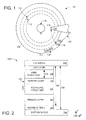
- FIG. 1 displays a top view block representation of an example data storage device 100 environment configured in accordance with some embodiments. While not limiting or required, the data storage device 100 has an actuating assembly 102 that is capable of positioning a transducing head 104 over a variety of locations on a magnetic storage media 106 where stored data bits 108 are located on predetermined data tracks 110. Each data track 110 may be configured with a width 112 that corresponds with an areal density that determines the storage capacity of the media 106.
- Movement of the storage media 106 can be facilitated through attachment to one or more spindle motors 114 that rotate during use to produce an air bearing surface (ABS) on which a slider portion 116 of the actuating assembly 102 flies to position a head gimbal assembly (HGA) 118, which includes the transducing head 104, over a predetermined portion of the media 106.
- the transducing head 104 can be configured with one or more transducing elements, such as a magnetic writer, magnetically responsive reader, and magnetic shields, which operate to program and read data from the selected data tracks 110 of the storage media 106, respectively. In this way, controlled motion of the actuating assembly 102 correspond with alignment of the transducers with the data tracks 110 defined on the storage media surfaces to write, read, and rewrite data.
- FIG. 2 shows a cross-sectional block representation of an example transducing element 120 capable of being used in the data storage device 100 of FIG. 1 .
- the transducing element 120 has a magnetic stack 122 disposed between bottom 124 and top 126 magnetic shields on an ABS.
- the magnetic stack 122 can be characterized as a spin valve due to the presence of a fixed magnetization pinning layer 128 contacting a fixed magnetization reference structure 130 opposite a non-magnetic barrier layer 132 from a magnetically free structure 134 with the structures 130 and 134 each possibly being single layers and laminations of magnetic and non-magnetic sub-layers.
- the non-magnetic barrier layer 132 may be formed as an oxide barrier like MgO and alumina or, alternatively, be constructed as spacer layer of non-magnetic material, such as Cu or Ag.
- a magnetic seed 136 can be positioned on opposite sides of the stack 122 to provide predetermined grain growth and magnetic properties, such as anisotropy, in the pinning layer 128.
- Construction of the spin valve magnetic stack 122 can have a physical shield-to-shield spacing 138, magnetic shield-to-shield spacing 140 used to determine P50 measurements, and free structure thickness 142 that determines the magnetic extent of the magnetic stack 122 and the possible data track resolution.
- the magnetic stack 122 may be configured, as shown, with a magnetic seed 136 that can act as a magnetic shield and reduce the effective magnetic shield-to-shield spacing 140 of the transducing element 120.
- the inclusion of the magnetic seed 136 may induce magnetic volatility as stray magnetic fields inadvertently shift the magnetization of the magnetic seed 136, which can be problematic in data storage environments where the data bits are densely packed and stray magnetic fields can be prevalent and relatively intense.
- the inadvertent magnetic domain movement of the magnetic seed 136 and resultant noise that can degrade magnetic stack 122 performance from the presence of stray magnetic fields has emphasized an ability to stabilize the magnetic seed 136 without adding to the magnetic shield-to-shield spacing 140 of the transducing element 120.
- the bottom shield 124 can be configured to stabilize the magnetic seed 136 and optimize magnetic stack 122 magnetic operations by minimizing the magnetic seed's 136 sensitivity to stray magnetic fields.
- stack is an unlimited term within this disclosure that can be one or more vertically and horizontally aligned layers, constructed of magnetic and non-magnetic material that are capable of magnetic reading.
- the term “stack” will be understood to mean a component that is constructed to respond to external data bits.
- a magnetic stack may be a data reader that can differentiate between a plurality of data bits.
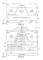
- FIG. 3 generally illustrates an air bearing view block representation of an example data reader 150 with such a configuration.
- the data reader 150 has a magnetic stack 152 disposed between lateral side shields 154 and vertically between bottom 156 and top 158 shields.
- the bottom shield 156 has a fixed magnetization structure 160 that may be a single ferromagnetic layer or a lamination of magnetic and non-magnetic sub-layers which is fixed by an antiferromagnet (AFM) 162.
- AFM antiferromagnet
- the fixed magnetization provided by the AFM 162 and fixed magnetization structure 160 can stabilize portions of the magnetic stack 152 and allow for a reduced shield-to-shield spacing as reference structures of the magnetic stack can have decreased thicknesses
- the tuned thickness 166 of the AFM layer 162 can provide fixed magnetization for the bottom shield 156 that maintains shield functionality for blocking stray magnetic fields while stabilizing both the fixed magnetization structure 160 and the magnetic stack 152.
- the AFM layer 162 can be further tuned for material and coercivity to provide a predetermined magnetic strength and orientation to set the magnetization of the bottom shield 156 and fixed magnetization structure 160 without interfering with the ability of the magnetic stack 152 to accurately sense external data bits.
- FIG. 4 displays an air bearing view block representation of a portion of an example transducing element 180 constructed in accordance with various embodiments to produce a fixed shield magnetization 182 in the bottom shield 184 that stabilizes a magnetic seed 186 of the magnetic stack 188 via contacting adjacency.
- Various embodiments may configure the fixed magnetization structure 190 to tune the strength and orientation of the fixed shield magnetization 182 to stabilize other portions of the magnetic stack 188, such as the AFM 192, first and second ferromagnetic SAF layers 194, and free layer 196.
- Such fixed magnetization 182 tuning may be conducted by sizing the fixed magnetization structure 190, including the ferromagnetic SAF layers 198 separated by a non-magnetic spacer layer 200, with a width 202 at the ABS that is greater than an average 204 and greatest 208 stack width.
- the exchange coupling provided by the contact of the magnetic seed 186 and synthetic antiferromagnet (SAF) fixed magnetization structure 190 can allow for simple, efficient production of the fixed magnetization 182 for the bottom shield 184 as ferromagnetic exchange coupling limits magnetic domain movement in the magnetic seed 186 while RKKY coupling present in the fixed magnetization structure 190 limits magnetic domain movement in the bottom shield 184.
- the bottom shield 184 can operate in concert with side shields 208 positioned on opposite lateral sides of the magnetic stack 186 to define a magnetic extent of the free layer 196 that allows a single data bit to be sensed with a reduced shield-to-shield spacing 210 despite high areal data bit density.
- the ability to tune the fixed magnetization 182 of the bottom shield 184 for strength and orientation can provide diverse magnetic stack 188 shielding that allows transducing element 180 optimization for a variety of different data storage environments.
- the bottom shield 184 can be configured with a fixed magnetization 182 that is parallel to the ABS and Z axis, as shown, which can provide efficient shielding characteristics without degrading free layer 196 sensitivity.
- an orthogonal or canted fixed magnetization orientation such as an angle of approximately +/-10-80° with respect to the Z axis, can be utilized to tune the stabilization of the magnetic seed 186 while providing a bias magnetization for the magnetic stack 188.
- FIGS. 5A and 5B respectively illustrate an example data reader fabrication routine 220 carried out in accordance with some embodiments.
- step 222 begins by depositing a shield layer and SAF structure that can function together as single bottom shield lamination.
- the example sheet film lamination 242 of FIG. 5B corresponds to step 222 and displays how a shield layer 262 can be formed atop a basecoat 264 and between insulating layers 266 with a SAF lamination 268 and stop layer 270 continuously spanning across the lateral insulating layers 266 above the shield layer 262.
- Step 224 of FIG. 5A proceeds to pattern the SAF structure to be the same width at the ABS as the bottom shield, as shown by sheet film lamination 244 of FIG. 5B where a pattern 272 is aligned with the shield layer 262 atop the stop layer 270. Positioning of the pattern 272 allows step 226 of FIG. 5A to mill the stop layer 270 and SAF structure 268 to be the same size as the bottom shield, which can allow the SAF structure 268 to be more uniformly incorporated into the bottom shield.
- Various embodiments of step 226 further replace the removed portions of the SAF structure and stop layer 270, with the SAF structure by second insulating layers 274 that are vertically aligned with the first insulating layers 266.
- Routine 220 then backfills a stop layer 276 and insulator material 278 about the pattern 272 in step 228, as displayed by sheet film lamination 248.
- the backfilling of material about the pattern 272, as shown, can allow for a lift off process to be conducted in step 230 instead of a knock off pattern removal.
- Such a lift off process can be simpler with less topography than a knock off process and allow a controlled chemical mechanical polish (CMP) to be conducted with predetermined parameters, like lower polish rate than for alumina and long enough duration to ensure a smooth SAF surface with no undersprayed insulating material and without damage to the SAF structure.
- CMP controlled chemical mechanical polish
- the predetermined parameters can be tuned in accordance with various embodiments to provide magnetic stack grain growth that results in grains of a predetermined size, such as less than 12nm grains.
- step 232 may conduct an annealing operation that sets a magnetization orientation in the respective magnetic structures 262 and 268, such as the magnetizations of FIG. 4 .
- the annealing operation of step 232 can act to optimize SAF 268 surface roughness to provide predetermined grain sizes.
- Step 234 can subsequently etch the stop layer 270 during a magnetic stack pre-etching operation, which corresponds with sheet film lamination 254 of FIG. 5B . It should be noted that step 234 may be conducted in concert or independently of annealing operations on a magnetic stack.
- the plurality of annealing operations that may be applied to the shield layer 262 and serially rotate the orientation of the bottom shield fixed magnetization parallel and orthogonal to the ABS can be planned so that a predetermined fixed magnetization orientation is achieved, such as an orientation parallel to the ABS as illustrated in FIG. 4 .
- the formatting and tuning of the SAF 268 and shield layer 262 through various lithography and annealing operations is culminated through steps 236 and 238 that respectively deposit and pattern a magnetic stack lamination 280, like the spin valve stack 122 of FIG. 2 , and a top magnetic shield 282 atop the prepared SAF surface.
- the sheet film lamination 258 generally shows how such steps could produce a data transducing element that is stabilized through bias magnetization provided by the SAF 268 abutted and included in the shield layer 262.
- the various steps of routine 220 are not required or limited. For instance, an additional annealing operation may be conducted with after deposition and patterning of the magnetic stack in step 236 to set the fixed magnetization orientation of the SAF 268 and portions of the magnetic stack 280.
- a bottom shield Through tuned design and construction of a bottom shield to have a predetermined fixed magnetization strength and orientation, magnetic operation of the magnetic stack can be stabilized.
- the ability to configure the bottom shield with a fixed magnetization with a variety of magnetic orientations provided by annealing operations can allow diverse applications for magnetic shielding and biasing of the magnetic stack.
- the variety of different magnetic strengths afforded by the tuned size, material, and position of the fixed magnetization structure of the bottom shield allows the magnetic stack to reliably respond to high data bity density data storage environments as magnetic noise from a magnetic seed portion of the magnetic stack is minimized.
Landscapes
- Engineering & Computer Science (AREA)
- Manufacturing & Machinery (AREA)
- Magnetic Heads (AREA)
- Hall/Mr Elements (AREA)
Abstract
Description
- Various embodiments are generally directed to a transducing element capable of reading data bits at least from a rotating data storage medium.
- In accordance with some embodiments, a magnetic stack may have free and fixed magnetization structures atop a magnetic seed layer. A bottom shield may be positioned contactingly adjacent the magnetic stack opposite a top shield with the bottom shield having a fixed pinning magnetization set to a predetermined magnetic orientation.
- According to a first aspect of the present invention, there is provided an apparatus comprising: a magnetic stack comprising free and fixed magnetization structures atop a magnetic seed layer; and a bottom shield contactingly adjacent the magnetic stack opposite a top shield, the bottom shield comprising a fixed pinning magnetization set to a predetermined magnetic orientation.
- Preferably, the fixed magnetization structure of the magnetic stack comprises a synthetic antiferromagnet (SAF).
- Preferably, an antiferromagnet (AFM) is disposed between the magnetic seed and the fixed magnetization structure of the magnetic stack.
- Preferably, the fixed pinning magnetization is set by a synthetic antiferromagnet (SAF) in the bottom shield.
- Preferably, an antiferromagnet (AFM) is disposed between the SAF and a shield seed layer in the bottom shield.
- Preferably, the shield seed layer has a predetermined texture corresponding to the predetermined magnetic orientation.
- Preferably, the bottom shield has a wider width at an air bearing surface (ABS) than an average width of the magnetic stack.
- Preferably, the predetermined magnetic orientation is parallel to an air bearing surface (ABS).
- Preferably, the magnetic stack is disposed between side shields.
- Preferably, the each side shield is separated from the magnetic stack by an insulating layer.
- Preferably, each insulating layer continuously extends to separate the side shield from the bottom shield.
- Preferably, each side shield continuously extends from the free magnetization structure of the magnetic stack to the top shield.
- According to another aspect of the present invention, there is provided a data reader comprising: a magnetic stack comprising free and fixed magnetization structures atop a magnetic seed layer; and a bottom shield contactingly adjacent and coupled to the magnetic stack opposite a top shield, the bottom shield comprising a fixed pinning magnetization set to a predetermined magnetic orientation.
- Preferably, the bottom shield is coupled to the magnetic seed layer of the magnetic stack.
- Preferably, the predetermined magnetic orientation matches a fixed magnetization orientation of the fixed magnetization structure of the magnetic stack.
- Preferably, the magnetic seed of the magnetic stack contacts a first ferromagnetic layer of the bottom layer, the first ferromagnetic layer separated from a second ferromagnetic layer by a non-magnetic spacer layer as part of a synthetic antiferromagnet (SAF).
- According to another aspect of the present invention, there is provided a method comprising: forming a magnetic stack comprising free and fixed magnetization structures atop a magnetic seed layer; contact the magnetic stack with a bottom shield opposite a top shield, the bottom shield comprising a fixed pinning magnetization set to a predetermined magnetic orientation.
- Preferably, the magnetic stack exclusively undergoes a first annealing operation.
- Preferably, the predetermined magnetic orientation is provided by a second annealing operation conducted on the bottom shield and magnetic stack subsequent to the first annealing operation.
- Preferably, the first and second annealing operations configure the fixed pinning magnetizations to different, orthogonal orientations.
- Embodiments of the present invention will now be described by way of further example only and with reference to the accompanying drawings, in which:
-
FIG. 1 is a block representation of an example portion of a data storage device configured and operated in accordance with some embodiments. -
FIG. 2 shows a cross-sectional block representation of a portion of an example transducing element capable of being used in the data storage device ofFIG. 1 . -
FIG. 3 displays an air bearing view block representation of a portion of an example data reader constructed in accordance with various embodiments. -
FIG. 4 shows an air bearing portion of an example transducing element configured in accordance with some embodiments. -
FIGS. 5A and 5B illustrate an example data reader fabrication routine carried out in accordance with various embodiments. - Faster data access and higher data capacity in data storage devices with reduced form factors has corresponded with data transducing components formed on a microscopic scale. The minimization of magnetic layers and shields in a data reading element can contribute to the production of noise that can degrade magnetic performance. Added emphasis on reducing the physical size of a magnetic lamination while maintaining separate magnetic operation of shields and data sensing layers has corresponded with volatile magnetic stability that jeopardizes reliable data reading. Hence, industry continues to strive for physically smaller data reading laminations that are magnetically stable with minimal noise production during operation
- Accordingly, a data reader may be configured at least with a magnetic stack having free and fixed magnetization structures atop a magnetic seed layer with a bottom shield contactingly adjacent the magnetic stack opposite a top shield and the bottom shield configured with a fixed pinning magnetization set to a predetermined magnetic orientation. The ability to tune the fixed pinning magnetization allows for the stabilization of the magnetic seed of the magnetic stack. Such stabilization can lead to optimized magnetic stack performance as stray magnetic fields are less likely to produce noise and affect free magnetization structure operation.
- A tuned bottom shield and stabilized magnetic seed layer may be utilized in an unlimited variety of data storage environments, but
FIG. 1 displays a top view block representation of an exampledata storage device 100 environment configured in accordance with some embodiments. While not limiting or required, thedata storage device 100 has anactuating assembly 102 that is capable of positioning a transducinghead 104 over a variety of locations on amagnetic storage media 106 where storeddata bits 108 are located on predetermined data tracks 110. Each data track 110 may be configured with awidth 112 that corresponds with an areal density that determines the storage capacity of themedia 106. - Movement of the
storage media 106 can be facilitated through attachment to one ormore spindle motors 114 that rotate during use to produce an air bearing surface (ABS) on which aslider portion 116 of theactuating assembly 102 flies to position a head gimbal assembly (HGA) 118, which includes the transducinghead 104, over a predetermined portion of themedia 106. The transducinghead 104 can be configured with one or more transducing elements, such as a magnetic writer, magnetically responsive reader, and magnetic shields, which operate to program and read data from the selected data tracks 110 of thestorage media 106, respectively. In this way, controlled motion of the actuatingassembly 102 correspond with alignment of the transducers with the data tracks 110 defined on the storage media surfaces to write, read, and rewrite data. -
FIG. 2 shows a cross-sectional block representation of an example transducingelement 120 capable of being used in thedata storage device 100 ofFIG. 1 . The transducingelement 120 has amagnetic stack 122 disposed betweenbottom 124 and top 126 magnetic shields on an ABS. Themagnetic stack 122 can be characterized as a spin valve due to the presence of a fixedmagnetization pinning layer 128 contacting a fixedmagnetization reference structure 130 opposite anon-magnetic barrier layer 132 from a magneticallyfree structure 134 with thestructures non-magnetic barrier layer 132 may be formed as an oxide barrier like MgO and alumina or, alternatively, be constructed as spacer layer of non-magnetic material, such as Cu or Ag. - As the
free structure 134 responds to an external data bit while thereference structure 130 maintains a fixed magnetization due to coupling with thepinning layer 128, an external data bit can be read as a logic state. Through various tuned configurations, amagnetic seed 136 can be positioned on opposite sides of thestack 122 to provide predetermined grain growth and magnetic properties, such as anisotropy, in thepinning layer 128. Construction of the spin valvemagnetic stack 122 can have a physical shield-to-shield spacing 138, magnetic shield-to-shield spacing 140 used to determine P50 measurements, andfree structure thickness 142 that determines the magnetic extent of themagnetic stack 122 and the possible data track resolution. - The
magnetic stack 122 may be configured, as shown, with amagnetic seed 136 that can act as a magnetic shield and reduce the effective magnetic shield-to-shield spacing 140 of the transducingelement 120. However, the inclusion of themagnetic seed 136 may induce magnetic volatility as stray magnetic fields inadvertently shift the magnetization of themagnetic seed 136, which can be problematic in data storage environments where the data bits are densely packed and stray magnetic fields can be prevalent and relatively intense. The inadvertent magnetic domain movement of themagnetic seed 136 and resultant noise that can degrademagnetic stack 122 performance from the presence of stray magnetic fields has emphasized an ability to stabilize themagnetic seed 136 without adding to the magnetic shield-to-shield spacing 140 of the transducingelement 120. Thus, thebottom shield 124 can be configured to stabilize themagnetic seed 136 and optimizemagnetic stack 122 magnetic operations by minimizing the magnetic seed's 136 sensitivity to stray magnetic fields. - It should be noted that the term "stack" is an unlimited term within this disclosure that can be one or more vertically and horizontally aligned layers, constructed of magnetic and non-magnetic material that are capable of magnetic reading. Throughout the present application, the term "stack" will be understood to mean a component that is constructed to respond to external data bits. For example, but not in any way limiting, a magnetic stack may be a data reader that can differentiate between a plurality of data bits.
-
FIG. 3 generally illustrates an air bearing view block representation of anexample data reader 150 with such a configuration. As shown, thedata reader 150 has amagnetic stack 152 disposed betweenlateral side shields 154 and vertically betweenbottom 156 and top 158 shields. Thebottom shield 156 has afixed magnetization structure 160 that may be a single ferromagnetic layer or a lamination of magnetic and non-magnetic sub-layers which is fixed by an antiferromagnet (AFM) 162. The fixed magnetization provided by theAFM 162 andfixed magnetization structure 160 can stabilize portions of themagnetic stack 152 and allow for a reduced shield-to-shield spacing as reference structures of the magnetic stack can have decreased thicknesses - The tuned
thickness 166 of theAFM layer 162 can provide fixed magnetization for thebottom shield 156 that maintains shield functionality for blocking stray magnetic fields while stabilizing both thefixed magnetization structure 160 and themagnetic stack 152. Through various embodiments, theAFM layer 162 can be further tuned for material and coercivity to provide a predetermined magnetic strength and orientation to set the magnetization of thebottom shield 156 and fixedmagnetization structure 160 without interfering with the ability of themagnetic stack 152 to accurately sense external data bits. -
FIG. 4 displays an air bearing view block representation of a portion of anexample transducing element 180 constructed in accordance with various embodiments to produce a fixedshield magnetization 182 in thebottom shield 184 that stabilizes amagnetic seed 186 of themagnetic stack 188 via contacting adjacency. Various embodiments may configure the fixedmagnetization structure 190 to tune the strength and orientation of the fixedshield magnetization 182 to stabilize other portions of themagnetic stack 188, such as theAFM 192, first and second ferromagnetic SAF layers 194, andfree layer 196. Suchfixed magnetization 182 tuning may be conducted by sizing the fixedmagnetization structure 190, including the ferromagnetic SAF layers 198 separated by anon-magnetic spacer layer 200, with awidth 202 at the ABS that is greater than an average 204 and greatest 208 stack width. - The exchange coupling provided by the contact of the
magnetic seed 186 and synthetic antiferromagnet (SAF) fixedmagnetization structure 190 can allow for simple, efficient production of the fixedmagnetization 182 for thebottom shield 184 as ferromagnetic exchange coupling limits magnetic domain movement in themagnetic seed 186 while RKKY coupling present in the fixedmagnetization structure 190 limits magnetic domain movement in thebottom shield 184. Despite the fixedmagnetization 182,wider width 202, and laminated structure, thebottom shield 184 can operate in concert withside shields 208 positioned on opposite lateral sides of themagnetic stack 186 to define a magnetic extent of thefree layer 196 that allows a single data bit to be sensed with a reduced shield-to-shield spacing 210 despite high areal data bit density. - The ability to tune the fixed
magnetization 182 of thebottom shield 184 for strength and orientation can provide diversemagnetic stack 188 shielding that allows transducingelement 180 optimization for a variety of different data storage environments. For example, thebottom shield 184 can be configured with a fixedmagnetization 182 that is parallel to the ABS and Z axis, as shown, which can provide efficient shielding characteristics without degradingfree layer 196 sensitivity. In some embodiments, an orthogonal or canted fixed magnetization orientation, such as an angle of approximately +/-10-80° with respect to the Z axis, can be utilized to tune the stabilization of themagnetic seed 186 while providing a bias magnetization for themagnetic stack 188. - While such fixed magnetization tuning can occur at any time and with any combination of manufacturing steps,
FIGS. 5A and 5B respectively illustrate an example datareader fabrication routine 220 carried out in accordance with some embodiments. In the embodiment shown inFIG. 5A ,step 222 begins by depositing a shield layer and SAF structure that can function together as single bottom shield lamination. The examplesheet film lamination 242 ofFIG. 5B corresponds to step 222 and displays how ashield layer 262 can be formed atop abasecoat 264 and between insulatinglayers 266 with aSAF lamination 268 and stoplayer 270 continuously spanning across the lateral insulatinglayers 266 above theshield layer 262. - Step 224 of
FIG. 5A proceeds to pattern the SAF structure to be the same width at the ABS as the bottom shield, as shown bysheet film lamination 244 ofFIG. 5B where apattern 272 is aligned with theshield layer 262 atop thestop layer 270. Positioning of thepattern 272 allowsstep 226 ofFIG. 5A to mill thestop layer 270 andSAF structure 268 to be the same size as the bottom shield, which can allow theSAF structure 268 to be more uniformly incorporated into the bottom shield. Various embodiments ofstep 226 further replace the removed portions of the SAF structure and stoplayer 270, with the SAF structure by second insulatinglayers 274 that are vertically aligned with the first insulatinglayers 266. -
Routine 220 then backfills astop layer 276 andinsulator material 278 about thepattern 272 instep 228, as displayed bysheet film lamination 248. The backfilling of material about thepattern 272, as shown, can allow for a lift off process to be conducted instep 230 instead of a knock off pattern removal. Such a lift off process can be simpler with less topography than a knock off process and allow a controlled chemical mechanical polish (CMP) to be conducted with predetermined parameters, like lower polish rate than for alumina and long enough duration to ensure a smooth SAF surface with no undersprayed insulating material and without damage to the SAF structure. The predetermined parameters can be tuned in accordance with various embodiments to provide magnetic stack grain growth that results in grains of a predetermined size, such as less than 12nm grains. - With the
SAF structure 268 andshield layer 262 having a predetermined texture,step 232 may conduct an annealing operation that sets a magnetization orientation in the respectivemagnetic structures FIG. 4 . The annealing operation ofstep 232 can act to optimizeSAF 268 surface roughness to provide predetermined grain sizes. Step 234 can subsequently etch thestop layer 270 during a magnetic stack pre-etching operation, which corresponds withsheet film lamination 254 ofFIG. 5B . It should be noted thatstep 234 may be conducted in concert or independently of annealing operations on a magnetic stack. The plurality of annealing operations that may be applied to theshield layer 262 and serially rotate the orientation of the bottom shield fixed magnetization parallel and orthogonal to the ABS can be planned so that a predetermined fixed magnetization orientation is achieved, such as an orientation parallel to the ABS as illustrated inFIG. 4 . - The formatting and tuning of the
SAF 268 andshield layer 262 through various lithography and annealing operations is culminated throughsteps magnetic stack lamination 280, like thespin valve stack 122 ofFIG. 2 , and a topmagnetic shield 282 atop the prepared SAF surface. Thesheet film lamination 258 generally shows how such steps could produce a data transducing element that is stabilized through bias magnetization provided by theSAF 268 abutted and included in theshield layer 262. The various steps of routine 220 are not required or limited. For instance, an additional annealing operation may be conducted with after deposition and patterning of the magnetic stack instep 236 to set the fixed magnetization orientation of theSAF 268 and portions of themagnetic stack 280. - Through tuned design and construction of a bottom shield to have a predetermined fixed magnetization strength and orientation, magnetic operation of the magnetic stack can be stabilized. The ability to configure the bottom shield with a fixed magnetization with a variety of magnetic orientations provided by annealing operations can allow diverse applications for magnetic shielding and biasing of the magnetic stack. Moreover, the variety of different magnetic strengths afforded by the tuned size, material, and position of the fixed magnetization structure of the bottom shield allows the magnetic stack to reliably respond to high data bity density data storage environments as magnetic noise from a magnetic seed portion of the magnetic stack is minimized.
- While the embodiments herein have been directed to magnetic sensing, it will be appreciated that the technology described above can readily be utilized in any number of other applications, including data writing. It is to be understood that even though numerous characteristics of various embodiments of the present disclosure have been set forth in the foregoing description, together with details of the structure and function of various embodiments, this detailed description is illustrative only, and changes may be made in detail, especially in matters of structure and arrangements of parts within the principles of the present technology to the full extent indicated by the broad general meaning of the terms in which the appended claims are expressed. For example, the particular elements may vary depending on the particular application without departing from the scope of the present disclosure.
Claims (20)
- An apparatus comprising:a magnetic stack (188) comprising free (196) and fixed magnetization structures (194) atop a magnetic seed layer (186); anda bottom shield (184) contactingly adjacent the magnetic stack opposite a top shield, the bottom shield comprising a fixed pinning magnetization (190) set to a predetermined magnetic orientation.
- The apparatus of claim 1, wherein the fixed magnetization structure of the magnetic stack comprises a synthetic antiferromagnet (SAF) (194).
- The apparatus of claim 2, wherein an antiferromagnet (AFM) (192) is disposed between the magnetic seed (186) and the fixed magnetization structure (194) of the magnetic stack.
- The apparatus of any one of the preceding claims, wherein the fixed pinning magnetization is set by a synthetic antiferromagnet (SAF) (198) in the bottom shield.
- The apparatus of claim 4, wherein an antiferromagnet (AFM) is disposed between the SAF and a shield seed layer in the bottom shield.
- The apparatus of claim 5, wherein the shield seed layer has a predetermined texture corresponding to the predetermined magnetic orientation.
- The apparatus of any one of the preceding claims, wherein the bottom shield has a wider width (202) at an air bearing surface (ABS) than an average width (206) of the magnetic stack.
- The apparatus of any one of the preceding claims, wherein the predetermined magnetic orientation is parallel to an air bearing surface (ABS).
- The apparatus of any one of the preceding claims, wherein the magnetic stack is disposed between side shields (208).
- The apparatus of claim 9, wherein the each side shield is separated from the magnetic stack by an insulating layer.
- The apparatus of claim 10, wherein each insulating layer continuously extends to separate the side shield from the bottom shield.
- The apparatus of any one of claims 9 to 11, wherein each side shield continuously extends from the free magnetization structure of the magnetic stack to the top shield.
- The apparatus of any one of the preceding claims, wherein the bottom shield (184) is coupled to the magnetic seed layer (186) of the magnetic stack.
- The apparatus of any one of the preceding claims, wherein the predetermined magnetic orientation matches a fixed magnetization orientation of the fixed magnetization structure of the magnetic stack.
- The apparatus of any one of the preceding claims, wherein the magnetic seed layer (186) of the magnetic stack contacts a first ferromagnetic layer (198) of the bottom shield (184), the first ferromagnetic layer separated from a second ferromagnetic layer by a non-magnetic spacer layer (200) as part of a synthetic antiferromagnet (SAF).
- The apparatus of any one of the preceding claims, wherein the apparatus is a data reader and the bottom shield is coupled to the magnetic stack.
- A method comprising:forming a magnetic stack (188) comprising free (196) and fixed (194) magnetization structures atop a magnetic seed layer (186);contacting the magnetic stack with a bottom shield (184) opposite a top shield, the bottom shield comprising a fixed pinning magnetization (190) set to a predetermined magnetic orientation.
- The method of claim 17, wherein the magnetic stack exclusively undergoes a first annealing operation.
- The method of claim 18, wherein the predetermined magnetic orientation is provided by a second annealing operation conducted on the bottom shield and magnetic stack subsequent to the first annealing operation.
- The method of claim 19, wherein the first and second annealing operations configure the fixed pinning magnetizations to different, orthogonal orientations.
Applications Claiming Priority (1)
| Application Number | Priority Date | Filing Date | Title |
|---|---|---|---|
| US13/844,813 US20140268417A1 (en) | 2013-03-16 | 2013-03-16 | Bottom shield stabilized magnetic seed layer |
Publications (2)
| Publication Number | Publication Date |
|---|---|
| EP2779167A2 true EP2779167A2 (en) | 2014-09-17 |
| EP2779167A3 EP2779167A3 (en) | 2014-10-01 |
Family
ID=50391005
Family Applications (1)
| Application Number | Title | Priority Date | Filing Date |
|---|---|---|---|
| EP20140160342 Ceased EP2779167A3 (en) | 2013-03-16 | 2014-03-17 | Bottom shield stabilized magnetic seed layer |
Country Status (5)
| Country | Link |
|---|---|
| US (2) | US20140268417A1 (en) |
| EP (1) | EP2779167A3 (en) |
| JP (1) | JP6126030B2 (en) |
| KR (1) | KR20140113371A (en) |
| CN (1) | CN104050978A (en) |
Families Citing this family (12)
| Publication number | Priority date | Publication date | Assignee | Title |
|---|---|---|---|---|
| US9251816B2 (en) * | 2013-10-03 | 2016-02-02 | Seagate Technology Llc | Magnetic sensor shield pinned by a high-coercivity ferromagnet |
| US9269381B1 (en) | 2014-09-15 | 2016-02-23 | Seagate Technology Llc | Sensor structure having layer with high magnetic moment |
| US9171559B1 (en) | 2014-09-15 | 2015-10-27 | Seagate Technology Llc | Sensor structure with pinned stabilization layer |
| US9454979B1 (en) | 2014-11-14 | 2016-09-27 | Seagate Technology Llc | Sensor structure with multilayer top shield |
| US9666214B1 (en) * | 2015-09-23 | 2017-05-30 | Western Digital (Fremont), Llc | Free layer magnetic reader that may have a reduced shield-to-shield spacing |
| US9552834B1 (en) * | 2015-09-28 | 2017-01-24 | Seagate Technology Llc | Stabilization of one or more upper sensors in multi-sensor readers |
| US9870791B1 (en) * | 2016-04-15 | 2018-01-16 | Seagate Technology Llc | Stabilization of one or more upper sensors in multi-sensor readers |
| US10068601B1 (en) * | 2016-08-09 | 2018-09-04 | Western Digital (Fremont), Llc | Free layer only magnetic reader that may have a reduced shield-to-shield spacing and a multilayer side bias |
| US11423928B1 (en) | 2018-01-19 | 2022-08-23 | Seagate Technology Llc | Processing for forming single-grain near-field transducer |
| US10783907B1 (en) * | 2019-09-04 | 2020-09-22 | Seagate Technology Llc | Reader with bi-layered side shields |
| US12453292B2 (en) * | 2021-05-17 | 2025-10-21 | Institute of Microelectronics, Chinese Academy of Sciences | All-electrically-controlled spintronic neuron device, neuron circuit and neural network |
| US11881235B2 (en) * | 2022-02-22 | 2024-01-23 | Western Digital Technologies, Inc. | Leading shield for magnetic recording heads |
Family Cites Families (34)
| Publication number | Priority date | Publication date | Assignee | Title |
|---|---|---|---|---|
| JP3188212B2 (en) * | 1997-05-08 | 2001-07-16 | アルプス電気株式会社 | Thin film magnetic head |
| US7023670B2 (en) * | 2001-11-19 | 2006-04-04 | Alps Electric Co., Ltd. | Magnetic sensing element with in-stack biasing using ferromagnetic sublayers |
| JP3607678B2 (en) * | 2002-01-24 | 2005-01-05 | アルプス電気株式会社 | Magnetic detection element |
| US6961224B2 (en) * | 2003-09-24 | 2005-11-01 | Hitachi Global Storage Technologies Netherlands, B.V. | GMR enhancing seed layer for self pinned spin valves |
| US7606007B2 (en) * | 2006-02-17 | 2009-10-20 | Hitachi Global Storage Technologies Netherlands B.V. | Shield stabilization for magnetoresistive sensors |
| US7706108B2 (en) | 2006-02-24 | 2010-04-27 | Hitachi Global Storage Technologies Netherlands B.V. | Lead/shield structure for read head sensors |
| US8634162B2 (en) * | 2007-03-08 | 2014-01-21 | HGST Netherlands B.V. | Perpendicular write head having a stepped flare structure and method of manufacture thereof |
| US7768747B2 (en) * | 2007-04-16 | 2010-08-03 | Tdk Corporation | Thin-film magnetic head and manufacturing method thereof |
| US7869165B2 (en) * | 2007-07-30 | 2011-01-11 | Tdk Corporation | Magnetic field detecting element having stack with a plurality of free layers and side shield layers |
| US7916430B2 (en) * | 2007-08-09 | 2011-03-29 | Tdk Corporation | Thin-film magnetic head and manufacturing method thereof |
| US7974048B2 (en) * | 2007-11-28 | 2011-07-05 | Tdk Corporation | Magneto-resistive effect device of CPP type having shield layers coupled with ferromagnetic layers |
| US8305715B2 (en) * | 2007-12-27 | 2012-11-06 | HGST Netherlands, B.V. | Magnetoresistance (MR) read elements having an active shield |
| US9442171B2 (en) * | 2008-01-09 | 2016-09-13 | Seagate Technology Llc | Magnetic sensing device with reduced shield-to-shield spacing |
| US8514524B2 (en) * | 2008-05-09 | 2013-08-20 | Headway Technologies, Inc. | Stabilized shields for magnetic recording heads |
| US7961438B2 (en) | 2008-05-28 | 2011-06-14 | Tdk Corporation | Magnetoresistive device of the CPP type, and magnetic disk system |
| US8477461B2 (en) | 2008-07-29 | 2013-07-02 | Tdk Corporation | Thin film magnetic head having a pair of magnetic layers whose magnetization is controlled by shield layers |
| US8189303B2 (en) | 2008-08-12 | 2012-05-29 | Tdk Corporation | Thin film magnetic head having a pair of magnetic layers whose magnetization is controlled by shield layers |
| US8049997B2 (en) | 2008-09-29 | 2011-11-01 | Tdk Corporation | Magnetoresistive element including a pair of free layers coupled to a pair of shield layers |
| US20100149689A1 (en) | 2008-12-11 | 2010-06-17 | Tdk Corporation | Thin film magnetic head having a pair of magnetic layers whose magnetization is controlled by shield layer including amorphous layer |
| US8274764B2 (en) * | 2009-03-10 | 2012-09-25 | Tdk Corporation | Magneto-resistive effect element provided with GaN spacer layer |
| US8238063B2 (en) * | 2009-07-07 | 2012-08-07 | Seagate Technology Llc | Magnetoresistive sensor with synthetic antiferromagnetic cap or seed layers |
| US8125746B2 (en) * | 2009-07-13 | 2012-02-28 | Seagate Technology Llc | Magnetic sensor with perpendicular anisotrophy free layer and side shields |
| US8369048B2 (en) * | 2009-08-31 | 2013-02-05 | Tdk Corporation | CPP-type thin film magnetic head provided with side shields including a pair of antimagnetically exchanged-coupled side shield magnetic layers |
| US8514525B2 (en) * | 2010-09-13 | 2013-08-20 | HGST Netherlands B.V. | Current-perpendicular-to-the-plane (CPP) magnetoresistive (MR) sensor with reference layer integrated in magnetic shield |
| US8462467B2 (en) * | 2010-10-08 | 2013-06-11 | Tdk Corporation | Thin film magnetic head including soft layer magnetically connected with shield |
| US20120250189A1 (en) * | 2011-03-29 | 2012-10-04 | Tdk Corporation | Magnetic head including side shield layers on both sides of a mr element |
| US20120327537A1 (en) * | 2011-06-23 | 2012-12-27 | Seagate Technology Llc | Shield Stabilization Configuration With Applied Bias |
| US8582253B1 (en) * | 2012-06-04 | 2013-11-12 | Western Digital (Fremont), Llc | Magnetic sensor having a high spin polarization reference layer |
| JP5460792B2 (en) * | 2012-08-16 | 2014-04-02 | 株式会社東芝 | Magnetoresistive element, magnetic head, magnetic head assembly, magnetic recording / reproducing apparatus, and method of manufacturing magnetoresistive element |
| US8797692B1 (en) * | 2012-09-07 | 2014-08-05 | Western Digital (Fremont), Llc | Magnetic recording sensor with AFM exchange coupled shield stabilization |
| US8824107B2 (en) * | 2012-10-31 | 2014-09-02 | Seagate Technology Llc | Magnetic element with current constriction feature |
| US8921126B2 (en) * | 2013-01-25 | 2014-12-30 | Headway Technologies, Inc. | Magnetic seed method for improving blocking temperature and shield to shield spacing in a TMR sensor |
| US9633679B2 (en) * | 2014-05-06 | 2017-04-25 | Seagate Technology Llc | Sensor stack structure with RKKY coupling layer between free layer and capping layer |
| US9390735B1 (en) * | 2015-03-31 | 2016-07-12 | Seagate Technology Llc | Data reader side shield with differing stripe heights |
-
2013
- 2013-03-16 US US13/844,813 patent/US20140268417A1/en not_active Abandoned
-
2014
- 2014-03-06 KR KR20140026620A patent/KR20140113371A/en not_active Abandoned
- 2014-03-14 JP JP2014051951A patent/JP6126030B2/en active Active
- 2014-03-14 CN CN201410095508.4A patent/CN104050978A/en active Pending
- 2014-03-17 EP EP20140160342 patent/EP2779167A3/en not_active Ceased
-
2015
- 2015-07-14 US US14/799,354 patent/US9928857B2/en active Active
Non-Patent Citations (1)
| Title |
|---|
| None |
Also Published As
| Publication number | Publication date |
|---|---|
| EP2779167A3 (en) | 2014-10-01 |
| JP2014182868A (en) | 2014-09-29 |
| JP6126030B2 (en) | 2017-05-10 |
| US20150318004A1 (en) | 2015-11-05 |
| US20140268417A1 (en) | 2014-09-18 |
| US9928857B2 (en) | 2018-03-27 |
| CN104050978A (en) | 2014-09-17 |
| KR20140113371A (en) | 2014-09-24 |
Similar Documents
| Publication | Publication Date | Title |
|---|---|---|
| US9928857B2 (en) | Method of making a bottom shield stabilized magnetic seed layer | |
| US9390735B1 (en) | Data reader side shield with differing stripe heights | |
| US10354682B2 (en) | Thin data reader cap | |
| US9001474B2 (en) | Magnetic element with biasing structure distal the air bearing surface | |
| US7324310B2 (en) | Self-pinned dual CPP sensor exchange pinned at stripe back-end to avoid amplitude flipping | |
| US10186285B2 (en) | Data reader with front shield coupling structure | |
| US9082424B2 (en) | Side shield biasing layer separated from an air bearing surface | |
| KR101585989B1 (en) | Data reader with back edge surface | |
| US9899045B2 (en) | Data reader with pinned front shield | |
| US8737023B2 (en) | Magnetic reader with tuned anisotropy | |
| US8995096B2 (en) | Magnetic element side shield with diffusion barrier | |
| US20140133052A1 (en) | Magnetoresistive sensor having reduced read gap and strong pinned layer stability | |
| US9218826B1 (en) | Tuned horizontally symmetric magnetic stack | |
| CN104050989B (en) | The data reader side shield stopped with polishing | |
| JP5992972B2 (en) | Data reader having horizontal laminated shield and method for manufacturing the same | |
| US9017832B2 (en) | Magnetic element electrode lamination |
Legal Events
| Date | Code | Title | Description |
|---|---|---|---|
| PUAL | Search report despatched |
Free format text: ORIGINAL CODE: 0009013 |
|
| 17P | Request for examination filed |
Effective date: 20140424 |
|
| AK | Designated contracting states |
Kind code of ref document: A2 Designated state(s): AL AT BE BG CH CY CZ DE DK EE ES FI FR GB GR HR HU IE IS IT LI LT LU LV MC MK MT NL NO PL PT RO RS SE SI SK SM TR |
|
| AX | Request for extension of the european patent |
Extension state: BA ME |
|
| PUAI | Public reference made under article 153(3) epc to a published international application that has entered the european phase |
Free format text: ORIGINAL CODE: 0009012 |
|
| AK | Designated contracting states |
Kind code of ref document: A3 Designated state(s): AL AT BE BG CH CY CZ DE DK EE ES FI FR GB GR HR HU IE IS IT LI LT LU LV MC MK MT NL NO PL PT RO RS SE SI SK SM TR |
|
| AX | Request for extension of the european patent |
Extension state: BA ME |
|
| RIC1 | Information provided on ipc code assigned before grant |
Ipc: G11B 5/31 20060101AFI20140826BHEP Ipc: G11B 5/39 20060101ALI20140826BHEP |
|
| RBV | Designated contracting states (corrected) |
Designated state(s): AL AT BE BG CH CY CZ DE DK EE ES FI FR GB GR HR HU IE IS IT LI LT LU LV MC MK MT NL NO PL PT RO RS SE SI SK SM TR |
|
| 17Q | First examination report despatched |
Effective date: 20151117 |
|
| STAA | Information on the status of an ep patent application or granted ep patent |
Free format text: STATUS: THE APPLICATION HAS BEEN REFUSED |
|
| 18R | Application refused |
Effective date: 20171023 |