EP2775781A1 - Mobile communication terminal - Google Patents
Mobile communication terminal Download PDFInfo
- Publication number
- EP2775781A1 EP2775781A1 EP12844740.6A EP12844740A EP2775781A1 EP 2775781 A1 EP2775781 A1 EP 2775781A1 EP 12844740 A EP12844740 A EP 12844740A EP 2775781 A1 EP2775781 A1 EP 2775781A1
- Authority
- EP
- European Patent Office
- Prior art keywords
- signal
- port
- antenna
- transmitted
- receiving port
- Prior art date
- Legal status (The legal status is an assumption and is not a legal conclusion. Google has not performed a legal analysis and makes no representation as to the accuracy of the status listed.)
- Granted
Links
Images

Classifications
-
- H—ELECTRICITY
- H04—ELECTRIC COMMUNICATION TECHNIQUE
- H04B—TRANSMISSION
- H04B1/00—Details of transmission systems, not covered by a single one of groups H04B3/00 - H04B13/00; Details of transmission systems not characterised by the medium used for transmission
- H04B1/38—Transceivers, i.e. devices in which transmitter and receiver form a structural unit and in which at least one part is used for functions of transmitting and receiving
- H04B1/40—Circuits
-
- H—ELECTRICITY
- H04—ELECTRIC COMMUNICATION TECHNIQUE
- H04B—TRANSMISSION
- H04B1/00—Details of transmission systems, not covered by a single one of groups H04B3/00 - H04B13/00; Details of transmission systems not characterised by the medium used for transmission
- H04B1/005—Details of transmission systems, not covered by a single one of groups H04B3/00 - H04B13/00; Details of transmission systems not characterised by the medium used for transmission adapting radio receivers, transmitters andtransceivers for operation on two or more bands, i.e. frequency ranges
- H04B1/0053—Details of transmission systems, not covered by a single one of groups H04B3/00 - H04B13/00; Details of transmission systems not characterised by the medium used for transmission adapting radio receivers, transmitters andtransceivers for operation on two or more bands, i.e. frequency ranges with common antenna for more than one band
- H04B1/006—Details of transmission systems, not covered by a single one of groups H04B3/00 - H04B13/00; Details of transmission systems not characterised by the medium used for transmission adapting radio receivers, transmitters andtransceivers for operation on two or more bands, i.e. frequency ranges with common antenna for more than one band using switches for selecting the desired band
Definitions
- the present disclosure generally relates to the technical field of communications, and more particularly, to a mobile communication terminal.
- the existing 3G (3 rd -generation mobile communication technology)/4G (4 th -generation mobile communication technology) FDD (Frequency Division Duplexing) mobile terminals adopt a full duplex design, so the transmitting path and the receiving path thereof operate simultaneously.
- the duplexer is an essential device, which mainly functions to:
- the conventional duplexes have a relatively large insertion loss (IL); and especially in the case that the frequency is high and the transmitting frequency band is close to the receiving frequency band, the insertion loss is very large.
- IL insertion loss
- the duplexer used in WCDMA BC2 has an insertion loss of above 2.5 dB because the transmitting frequency band is 1850 MHz-1910 MHz and the receiving frequency band is 1930 MHz-1990 MHz.
- BPF band-pass filter
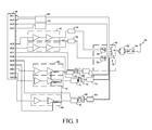
- the WCDMA+GSM dual-mode terminal mainly comprises an antenna 95, a duplexer 90, a wireless transceiver 10, a plurality of signal receiving branches and a plurality of signal transmitting branches.
- a GSM980/850 RX SAW module 20 and a DCS/PCS RX SAW module 30 are configured to receive an RF signal obtained by the antenna 95 and gated by the duplexer 90.
- the wireless transceiver 10 obtains the RF signal, which has been processed by the GSM980/850 RX SAW module 20, via a port 1011 and a port 1012, and obtains the RF signal, which has been processed by the DCS/PCS RX SAW module 30, via a port 1013 and a port 1014.
- a GSM HB PA (GSM High Band Power Amplifier) 40 and an HB MN (High Band Match Network) 41 constitute a GSM signal transmitting branch.
- the wireless transceiver 10 transmits a GSM high band (HB) signal via a port 1015 to the GSM HB PA 40 and the HB MN 41.
- the GSM HB PA 40 and the HB MN 41 perform power amplifying and network matching respectively on the GSM HB signal.
- the GSM HB signal which has been processed is transmitted by the antenna 95 after being gated by the duplexer 90.
- a GSM LB PA (GSM Low Band Power Amplifier) 50 and an LB MN (Low Band Match Network) 51 constitute another GSM signal transmitting branch.
- the wireless transceiver 10 transmits a GSM low band (LB) signal via a port 1016 to the GSM LB PA 50 and the LB MN 51.
- the GSM LB PA 50 and the LB MN 51 perform power amplifying and network matching respectively on the GSM LB signal.
- the GSM LB signal which has been processed is transmitted by the antenna 95 after being gated by the duplexer 90.
- a WCDMA BC1 PA (WCDMA BC1 Power Amplifier) 60, a W MN1 (WCDMA Match Network) 61, a duplexer 62 and a DPX MN (Duplexer Match Network) 63 constitute a WCDMA signal transmitting/receiving branch, which is configured to transmit or receive a WCDMA BC1 signal.
- the wireless transceiver 10 transmits a BC1 signal via a port 1019.
- the WCDMA BC1 PA 60, the W MN1 61 and the DPX MN 63 perform power amplifying and network matching respectively on the BC1 signal.
- the BC1 signal which has been processed is transmitted by the antenna 95 after being gated by the duplexer 90.
- the duplexer 62 can be used to select a path that allows the BC1 signal transmitted by the wireless transceiver 10 via the port 1019 to be transmitted via the antenna 95 or allows the wireless transceiver 10 to obtain a corresponding WCDMA signal from the antenna 95 via a port 1017.
- the wireless transceiver 10 generates a WCDMA BC2 signal and a WCDMA BC5 signal respectively via ports 1022 and 1023 and, via ports 1017 and 1018, obtains a BC2 signal and a BC5 signal received by the antenna 95 from the outside respectively.
- the ports 1022 and 1023 respectively correspond to two WCDMA signal transmitting branches
- the ports 1017 and 1018 respectively correspond to two WCDMA signal receiving branches.
- the architecture of the aforesaid WCDMA signal transmitting/receiving branch is completely the same as that of the aforesaid WCDMA signal transmitting/receiving branch corresponding to the BC1 signal, and thus will not be further described herein.
- an RF connector 92 and an ANT MN (Antenna Match Network) 94 are further provided between the antenna and the duplexer 90.
- the RF connector 92 and the ANT MN 94 are respectively configured to couple a plurality of signals from different signal sources into one signal and perform antenna matching on the signal.
- the duplexer 90 mainly functions to:
- the receiving path requires a high sensitivity (which is typically -110dBm in conventional technologies), while the transmitting path is a high-power path, the intensity of which can be up to 28dBm.
- OOB out-of-band
- the receiving system design for WCDMA signals of the mobile communication terminal shown in FIG. 1 is analyzed as follows:
- the power of the DPDCH (Dedicated Physical Data Channel) is -120.3dBm.
- the decoding threshold for QPSK modulation of the WCDAMA is 5.2dB, and a margin of 2dB needs to be reserved, so an input signal to noise ratio (SNR) of 7.2dB is required for the demodulation module.
- SNR signal to noise ratio
- the noise at the input end of the demodulation module is required to be below -173.343dBm/Hz.
- the typical output noise of the power amplifiers (60, 70 and 80) is:
- the present disclosure provides a mobile communication terminal to solve the problem of a relatively large insertion loss in the conventional duplexers.
- a mobile communication terminal which comprises: a first antenna, being configured to receive a radio frequency (RF) signal from the outside; a receiving acoustic surface wave filter, being configured to perform receiving acoustic surface wave filtering on the RF signal received by the first antenna; a wireless transceiver comprising a signal receiving port and a signal transmitting port, being configured to obtain the RF signal, on which the receiving acoustic surface wave filtering has been performed, from the receiving acoustic surface wave filter via the signal receiving port and amplifies a down-converted signal in the RF signal into a baseband signal; a baseband processor, being configured to obtain the baseband signal from the wireless transceiver and demodulate the baseband signal to generate a to-be-transmitted signal for transmission to the wireless transceiver; the wireless transceiver is further configured to convert the to-be-transmitted signal into an RF signal and output the RF signal from the signal transmitting port; a power amplifier
- the RF signal comprises a WCDMA BC1 signal, a WCDMA BC2 signal, a WCDMA BC5 signal and a WCDMA BC8 signal.
- the signal receiving port comprises a first signal receiving port, a second signal receiving port, a third signal receiving port and a fourth signal receiving port.
- the mobile communication terminal further comprises a first single-pole multi-throw (SPMT) switch disposed between the first antenna and the wireless transceiver to selectively connect one of the first signal receiving port, the second signal receiving port, the third signal receiving port and the fourth signal receiving port with the first antenna.
- SPMT single-pole multi-throw
- the to-be-transmitted RF signal comprises a to-be-transmitted WCDMA BC1 signal, a to-be-transmitted WCDMA BC2 signal or a to-be-transmitted WCDMA BC5 signal.
- the signal transmitting port comprises a first signal transmitting port, a second signal transmitting port and a third signal transmitting port.
- the mobile communication terminal further comprises a second SPMT switch disposed between the second antenna and the wireless transceiver to selectively connect one of the first signal transmitting port, the second signal transmitting port and the third signal transmitting port with the second antenna.
- a mobile communication terminal which comprises: a first antenna, being configured to receive a radio frequency (RF) signal from the outside; a wireless transceiver comprising a signal receiving port and a signal transmitting port, being configured to obtain the RF signal from the first antenna via the signal receiving port and amplifies a down-converted signal in the RF signal into a baseband signal; a baseband processor, being configured to obtain the baseband signal from the wireless transceiver and demodulate the baseband signal to generate a to-be-transmitted signal for transmission to the wireless transceiver; the wireless transceiver is further configured to convert the to-be-transmitted signal into an RF signal and output the RF signal from the signal transmitting port; and a second antenna, being configured to obtain the to-be-transmitted RF signal from the signal transmitting port and transmit the to-be-transmitted RF signal.
- RF radio frequency
- the mobile communication terminal further comprises a power amplifier disposed between the wireless transceiver and the second antenna.
- the power amplifier has an input end connected to the signal transmitting port and an output end connected to the second antenna.
- the power amplifier is configured to amplify the power of the to-be-transmitted RF signal output from the signal transmitting port, and output the to-be-transmitted RF signal of which the power has been amplified to the second antenna.
- the mobile communication terminal further comprises a low-pass filter (LPF) disposed between the power amplifier and the second antenna.
- the LPF is configured to perform low-pass filtering on the to-be-transmitted RF signal output from the output end of the power amplifier.
- the mobile communication terminal further comprises a receiving acoustic surface wave filter disposed between the first antenna and the wireless transceiver.
- the receiving acoustic surface wave filter is configured to perform receiving acoustic surface wave filtering on the RF signal received by the first antenna and output the RF signal, on which the receiving acoustic surface wave filtering has been performed, to the signal receiving port.
- the RF signal comprises a WCDMA BC1 signal, a WCDMA BC2 signal, a WCDMA BC5 signal and a WCDMA BC8 signal.
- the signal receiving port comprises a first signal receiving port, a second signal receiving port, a third signal receiving port and a fourth signal receiving port.
- the mobile communication terminal further comprises a first SPMT switch disposed between the first antenna and the wireless transceiver to selectively connect one of the first signal receiving port, the second signal receiving port, the third signal receiving port and the fourth signal receiving port with the first antenna.
- the to-be-transmitted RF signal comprises a to-be-transmitted WCDMA BC1 signal, a to-be-transmitted WCDMA BC2 signal or a to-be-transmitted WCDMA BC5 signal.
- the signal transmitting port comprises a first signal transmitting port, a second signal transmitting port and a third signal transmitting port.
- the mobile communication terminal further comprises a second SPMT switch disposed between the second antenna and the wireless transceiver to selectively connect one of the first signal transmitting port, the second signal transmitting port and the third signal transmitting port with the second antenna.
- the RF signal further comprises a GSM 900 signal, a GSM 850 signal and a GSM DCS signal.
- the signal receiving port comprises a fifth signal receiving port, a sixth signal receiving port and a seventh signal receiving port.
- the first SPMT switch further selectively connects one of the fifth signal receiving port, the sixth signal receiving port and the seventh signal receiving port with the first antenna.
- the to-be-transmitted RF signal further comprises a GSM HB signal and a GSM LB signal.
- the signal transmitting port further comprises a fourth signal transmitting port and a fifth signal transmitting port.
- the second SPMT switch further selectively connects one of the fourth signal transmitting port and the fifth signal transmitting port with the second antenna.
- the mobile communication terminal further comprises a broadband power coupler disposed between the first antenna and the second SPMT switch to detect a transmitting power of the to-be-transmitted RF signal.
- the low-pass filter, the second SPMT switch and the broadband power coupler are integrated into one chip.
- the present disclosure provides the following benefits: as compared to the prior art, the technical solutions of the present disclosure eliminate the need of a duplexer by providing a first antenna for receiving an RF signal from the outside and a second antenna for transmitting a to-be-transmitted RF signal. Therefore, the problem of insertion loss caused by using the duplexer is solved, thereby lowering the noise level in the transmitting path within the receiving frequency band. Additionally, the power consumption and heat generation of the system can be lowered and, meanwhile, the RF architecture can be simplified to lower the cost and achieve a more compact space.
- the present disclosure is especially adapted for platforms with relatively low output power.
- FIG. 2 is a schematic view illustrating a circuit structure of a mobile communication terminal according to a preferred embodiment of the present disclosure.
- the mobile communication terminal of the present disclosure comprises: a first antenna 101, being configured to receive an RF signal from the outside; a wireless transceiver 102 comprising a signal receiving port and a signal transmitting port, being configured to obtain the RF signal from the first antenna 101 via the signal receiving port and amplifies a down-converted signal in the RF signal into a baseband signal; a baseband processor (not shown), being configured to obtain the baseband signal from the wireless transceiver 102 and demodulate the baseband signal to generate a to-be-transmitted signal for transmission to the wireless transceiver 102; the wireless transceiver 102 is further configured to convert the to-be-transmitted signal into an RF signal and output the RF signal from the signal transmitting port; and a second antenna 103, being configured to obtain the to-be-transmitted RF
- the improvements of the present disclosure mainly lie in the first antenna 101, the second antenna 103 and the wireless transceiver 102, but not in the operating process and the connections between the baseband processor and the wireless transceiver 102. Therefore, the baseband processor is not shown in FIG. 2 .
- Power amplifiers 301, 302, 303, 304 and 305 are provided between the wireless transceiver 102 and the second antenna 103.
- Each of the power amplifiers 301, 302, 303, 304 and 305 has an input end connected to the signal transmitting port and an output end connected to the second antenna 103.
- Each of the power amplifiers 301, 302, 303, 304 and 305 is configured to amplify the power of the to-be-transmitted RF signal output from the signal transmitting port and output the to-be-transmitted RF signal of which the power has been amplified to the second antenna 103.
- Low-pass filters (LPFs) 401, 402, 403, 404 and 405 are disposed between the power amplifiers 301, 302, 303, 304 and 305 and the second antenna 103 respectively.
- the LPFs 401, 402, 403, 404 and 405 are configured to perform low-pass filtering on the to-be-transmitted RF signal output from the output end of the power amplifiers 301, 302, 303, 304 and 305 respectively.
- Receiving acoustic surface wave filters 200, 201, 202, 203 and 204 are disposed between the first antenna 101 and the wireless transceiver 102. Each of the receiving acoustic surface wave filters 200, 201, 202, 203 and 204 is configured to perform receiving acoustic surface wave filtering on the RF signal received by the first antenna 101 and output the RF signal, on which the receiving acoustic surface wave filtering has been performed, to the signal receiving port.
- the RF signal comprises a WCDMA BC8 signal, a WCDMA BC5 signal, a WCDMA BC2 signal and a WCDMA BC4 signal.
- the signal receiving port comprises a first signal receiving port 2011, a second signal receiving port 2012, a third signal receiving port 2014 and a fourth signal receiving port 2015.
- the mobile communication terminal further comprises a first SPMT switch 501 disposed between the first antenna 101 and the wireless transceiver 102 to selectively connect one of the first signal receiving port 2011, the second signal receiving port 2012, the third signal receiving port 2014 and the fourth signal receiving port 2015 with the first antenna 101.
- the to-be-transmitted RF signal comprises a to-be-transmitted WCDMA BC1 signal, a to-be-transmitted WCDMA BC2 signal or a to-be-transmitted WCDMA BC5 signal.
- the signal transmitting port comprises a first signal transmitting port 2016, a second signal transmitting port 2017 and a third signal transmitting port 2018.
- the mobile communication terminal further comprises a second SPMT switch 502 disposed between the second antenna 103 and the wireless transceiver 102 to selectively connect one of the first signal transmitting port, the second signal transmitting port and the third signal transmitting port with the second antenna 103.
- the RF signal further comprises a GSM 900 signal, a GSM 850 signal and a GSM DCS signal.
- the signal receiving port comprises a fifth signal receiving port 2011, a sixth signal receiving port 2012 and a seventh signal receiving port 2013.
- the fifth signal receiving port 2011 and the sixth signal receiving port 2012 can be multiplexed as the first signal receiving port 2011 and the second signal receiving port 2012.
- the first SPMT switch 501 further selectively connects one of the fifth signal receiving port 2011, the sixth signal receiving port 2012 and the seventh signal receiving port 2013 with the first antenna 101.
- the to-be-transmitted RF signal further comprises a GSM HB signal and a GSM LB signal.
- the signal transmitting port further comprises a fourth signal transmitting port 2019 and a fifth signal transmitting port 2020.
- the second SPMT switch 502 further selectively connects one of the fourth signal transmitting port 2019 and the fifth signal transmitting port 2020 with the second antenna 103.
- the mobile communication terminal further comprises a broadband power coupler 601 disposed between the first antenna 101 and the second SPMT switch 502 to detect a transmitting power of the to-be-transmitted RF signal.
- the power amplifiers 301, 302, 303, 304 and 305 (301, 302 and 303):
- the LPFs (401, 402 and 403):
- the second SPMT switch 502 The second SPMT switch 502:
- the broadband power coupler 601 The broadband power coupler 601:
- the RF transmitting line (not shown):
- the transmitting path falls on the first antenna 101 at the noise level of -173.5dBm/Hz at the receiving antenna. This satisfies the reception performance requirement for the entire system.
- the LPFs 401, 402, 403, 404 and 405, the second SPMT switch 502 and the broadband power coupler 601 are integrated into one chip. This can save the space and reduce the length of the RF transmission line to make the path between the output end of the power amplifier and the second antenna 103 as short as possible, thereby further reducing the insertion loss.
- CMOS Complementary Metal Oxide Semiconductor
- the present disclosure proposes a novel RF architecture for an FDD mobile communication terminal which eliminates the use of a duplexer. Therefore, the following advantages can be achieved:
- the present disclosure proposes a solution in which dual antennas are used.
- the transmitting path and the receiving path are separated and respectively communicate via one antenna. Since the separated antennas provide an isolation degree of about 10dB the required Rx Band Noise level of the transmitting path can be lowered.
- FIG. 2 The framework diagram of the RF architecture for this solution is shown in FIG. 2 . It should be noted that, this solution is especially suitable for a platform in which the wireless transceiver 102 has a relatively low output power.
- the technical solution of the present disclosure eliminates the need of a duplexer by providing the first antenna 101 for receiving an RF signal from the outside and the second antenna 103 for transmitting a to-be-transmitted RF signal. Therefore, the problem of insertion loss caused by using the duplexer is solved, thereby lowering the noise level in the transmitting path within the receiving frequency band. Additionally, the power consumption and heat generation of the system can be lowered and, meanwhile, the RF architecture can be simplified to lower the cost and achieve a more compact space. The present disclosure is especially suited for platforms with relatively low output power.
Landscapes
- Engineering & Computer Science (AREA)
- Computer Networks & Wireless Communication (AREA)
- Signal Processing (AREA)
- Transceivers (AREA)
Abstract
Description
- The present disclosure generally relates to the technical field of communications, and more particularly, to a mobile communication terminal.
- The existing 3G (3rd-generation mobile communication technology)/4G (4th-generation mobile communication technology) FDD (Frequency Division Duplexing) mobile terminals adopt a full duplex design, so the transmitting path and the receiving path thereof operate simultaneously. In the conventional FDD radio frequency (RF) architecture, the duplexer is an essential device, which mainly functions to:
- 1) combine the transmitting path and the receiving path together; and
- 2) perform filtering on the transmitting path and the receiving path.
- The conventional duplexes have a relatively large insertion loss (IL); and especially in the case that the frequency is high and the transmitting frequency band is close to the receiving frequency band, the insertion loss is very large. For example, the duplexer used in WCDMA BC2 (Wideband Code Division Multiple Access BC2) has an insertion loss of above 2.5 dB because the transmitting frequency band is 1850 MHz-1910 MHz and the receiving frequency band is 1930 MHz-1990 MHz. This requires use of a band-pass filter (BPF) having a central frequency of 1950 MHz and a transition frequency band of only 20 MHz, which is very difficult to be implemented.
- Such a great insertion loss leads to the following problems:
- 1) the problem of large power consumption. Because of the large insertion loss, the output power of the amplifier must be increased to ensure an adequate output power, and this will necessarily increase the power consumption.
- 2) the problem of heat dissipation. The increased output power and the increased power consumption will necessarily lead to generation of more heat. Heat generation of power amplifiers of the conventional WCDMA terminals is considerable, which has an influence on the battery and the user experience.
- 3) The problem of cost. Devices of high technical specifications necessarily have high cost.
- Referring to
FIG. 1 , an RF framework of a typical WCDMA+GSM dual-mode terminal is shown therein. The WCDMA+GSM dual-mode terminal mainly comprises anantenna 95, aduplexer 90, awireless transceiver 10, a plurality of signal receiving branches and a plurality of signal transmitting branches. - As two signal receiving branches, a GSM980/850
RX SAW module 20 and a DCS/PCSRX SAW module 30 are configured to receive an RF signal obtained by theantenna 95 and gated by theduplexer 90. Thewireless transceiver 10 obtains the RF signal, which has been processed by the GSM980/850RX SAW module 20, via aport 1011 and aport 1012, and obtains the RF signal, which has been processed by the DCS/PCSRX SAW module 30, via aport 1013 and aport 1014. - A GSM HB PA (GSM High Band Power Amplifier) 40 and an HB MN (High Band Match Network) 41 constitute a GSM signal transmitting branch. The
wireless transceiver 10 transmits a GSM high band (HB) signal via aport 1015 to the GSM HB PA 40 and the HB MN 41. The GSM HB PA 40 and the HB MN 41 perform power amplifying and network matching respectively on the GSM HB signal. The GSM HB signal which has been processed is transmitted by theantenna 95 after being gated by theduplexer 90. - A GSM LB PA (GSM Low Band Power Amplifier) 50 and an LB MN (Low Band Match Network) 51 constitute another GSM signal transmitting branch. The
wireless transceiver 10 transmits a GSM low band (LB) signal via aport 1016 to theGSM LB PA 50 and the LBMN 51. TheGSM LB PA 50 and the LB MN 51 perform power amplifying and network matching respectively on the GSM LB signal. The GSM LB signal which has been processed is transmitted by theantenna 95 after being gated by theduplexer 90. - A WCDMA BC1 PA (WCDMA BC1 Power Amplifier) 60, a W MN1 (WCDMA Match Network) 61, a
duplexer 62 and a DPX MN (Duplexer Match Network) 63 constitute a WCDMA signal transmitting/receiving branch, which is configured to transmit or receive a WCDMA BC1 signal. Thewireless transceiver 10 transmits a BC1 signal via aport 1019. The WCDMA BC1PA 60, theW MN1 61 and the DPX MN 63 perform power amplifying and network matching respectively on the BC1 signal. The BC1 signal which has been processed is transmitted by theantenna 95 after being gated by theduplexer 90. Theduplexer 62 can be used to select a path that allows the BC1 signal transmitted by thewireless transceiver 10 via theport 1019 to be transmitted via theantenna 95 or allows thewireless transceiver 10 to obtain a corresponding WCDMA signal from theantenna 95 via aport 1017. - Likewise, the
wireless transceiver 10 generates a WCDMA BC2 signal and a WCDMA BC5 signal respectively viaports ports antenna 95 from the outside respectively. Thus, theports ports - Additionally, an
RF connector 92 and an ANT MN (Antenna Match Network) 94 are further provided between the antenna and theduplexer 90. TheRF connector 92 and the ANTMN 94 are respectively configured to couple a plurality of signals from different signal sources into one signal and perform antenna matching on the signal. - In conventional mobile communication terminals, the
duplexer 90 mainly functions to: - 1) combine the transmitting path and the receiving path together; and
- 2) providing an isolation between the transmitting path and the receiving path, that is, attenuating the noise caused by the RF signal in the transmitting path within the receiving frequency band, thereby protecting receiving signals from the interference caused by the RF signal.
- The reason for the need of providing an isolation between the transmitting path and the receiving path is that, the receiving path requires a high sensitivity (which is typically -110dBm in conventional technologies), while the transmitting path is a high-power path, the intensity of which can be up to 28dBm. Because of the non-linearity of the RF system, there necessarily exists very intensive out-of-band (OOB) strays in the case that the main wave is 28dBm. Such strays will be directly fed to the receiving end if they are not isolated at the receiving frequency band, and the intensity thereof will be higher than that of the useful receiving signals. Finally, the receiving performance is influenced.
- The receiving system design for WCDMA signals of the mobile communication terminal shown in
FIG. 1 is analyzed as follows: - The typical receiving sensitivity of a conventional WCDAMA terminal is -110dBm.
- The power of the DPDCH (Dedicated Physical Data Channel) is -120.3dBm.
- The channel code rate for WCDMA sensitivity test is 12.2kbps, and the code gain is 10×log (3.84MHZ/12.2)=25dB.
- The decoding threshold for QPSK modulation of the WCDAMA is 5.2dB, and a margin of 2dB needs to be reserved, so an input signal to noise ratio (SNR) of 7.2dB is required for the demodulation module.
- Therefore, the noise at the input end of the demodulation module should be below:

- Taking a typical noise figure of 5dB of the
wireless transceiver 10 into consideration, the noise at the input end of the demodulation module is required to be below -173.343dBm/Hz. - The system thermal noise is:

where K (Boltzmann constant)=1.38×10⁻²⁰mJ/K, B=3.84MHz (65.843dB), T=290K. - The typical output noise of the power amplifiers (60, 70 and 80) is:
- 160dBm/Hz (the output of the wireless transceiver) +28dB (the typical amplifier gain of the amplifier at the receiving frequency band)

- Therefore, the
duplexer 90 is required to provide an isolation of at least 173.343-132= 41dB. - With such a great isolation, the insertion loss of the conventional duplexers is relatively large.
- Accordingly, an urgent need exists in the art to provide an antenna modulation method for a mobile communication terminal capable of solving the aforesaid problems.
- To solve the aforesaid technical problems, the present disclosure provides a mobile communication terminal to solve the problem of a relatively large insertion loss in the conventional duplexers.
- One technical solution of the present disclosure is to provide a mobile communication terminal, which comprises: a first antenna, being configured to receive a radio frequency (RF) signal from the outside; a receiving acoustic surface wave filter, being configured to perform receiving acoustic surface wave filtering on the RF signal received by the first antenna; a wireless transceiver comprising a signal receiving port and a signal transmitting port, being configured to obtain the RF signal, on which the receiving acoustic surface wave filtering has been performed, from the receiving acoustic surface wave filter via the signal receiving port and amplifies a down-converted signal in the RF signal into a baseband signal; a baseband processor, being configured to obtain the baseband signal from the wireless transceiver and demodulate the baseband signal to generate a to-be-transmitted signal for transmission to the wireless transceiver; the wireless transceiver is further configured to convert the to-be-transmitted signal into an RF signal and output the RF signal from the signal transmitting port; a power amplifier having an input end connected to the signal transmitting port, being configured to obtain the RF signal from the signal transmitting port, amplify the power of the to-be-transmitted RF signal, and output the to-be-transmitted RF signal of which the power has been amplified from an output end of the power amplifier; and a second antenna connected with the output end, being configured to obtain the to-be-transmitted RF signal from the output end and transmit the to-be-transmitted RF signal. The RF signal comprises a WCDMA BC1 signal, a WCDMA BC2 signal, a WCDMA BC5 signal and a WCDMA BC8 signal. The signal receiving port comprises a first signal receiving port, a second signal receiving port, a third signal receiving port and a fourth signal receiving port. The mobile communication terminal further comprises a first single-pole multi-throw (SPMT) switch disposed between the first antenna and the wireless transceiver to selectively connect one of the first signal receiving port, the second signal receiving port, the third signal receiving port and the fourth signal receiving port with the first antenna. The to-be-transmitted RF signal comprises a to-be-transmitted WCDMA BC1 signal, a to-be-transmitted WCDMA BC2 signal or a to-be-transmitted WCDMA BC5 signal. The signal transmitting port comprises a first signal transmitting port, a second signal transmitting port and a third signal transmitting port. The mobile communication terminal further comprises a second SPMT switch disposed between the second antenna and the wireless transceiver to selectively connect one of the first signal transmitting port, the second signal transmitting port and the third signal transmitting port with the second antenna.
- Another technical solution of the present disclosure is to provide a mobile communication terminal, which comprises: a first antenna, being configured to receive a radio frequency (RF) signal from the outside; a wireless transceiver comprising a signal receiving port and a signal transmitting port, being configured to obtain the RF signal from the first antenna via the signal receiving port and amplifies a down-converted signal in the RF signal into a baseband signal; a baseband processor, being configured to obtain the baseband signal from the wireless transceiver and demodulate the baseband signal to generate a to-be-transmitted signal for transmission to the wireless transceiver; the wireless transceiver is further configured to convert the to-be-transmitted signal into an RF signal and output the RF signal from the signal transmitting port; and a second antenna, being configured to obtain the to-be-transmitted RF signal from the signal transmitting port and transmit the to-be-transmitted RF signal.
- The mobile communication terminal further comprises a power amplifier disposed between the wireless transceiver and the second antenna. The power amplifier has an input end connected to the signal transmitting port and an output end connected to the second antenna. The power amplifier is configured to amplify the power of the to-be-transmitted RF signal output from the signal transmitting port, and output the to-be-transmitted RF signal of which the power has been amplified to the second antenna.
- The mobile communication terminal further comprises a low-pass filter (LPF) disposed between the power amplifier and the second antenna. The LPF is configured to perform low-pass filtering on the to-be-transmitted RF signal output from the output end of the power amplifier.
- The mobile communication terminal further comprises a receiving acoustic surface wave filter disposed between the first antenna and the wireless transceiver. The receiving acoustic surface wave filter is configured to perform receiving acoustic surface wave filtering on the RF signal received by the first antenna and output the RF signal, on which the receiving acoustic surface wave filtering has been performed, to the signal receiving port.
- The RF signal comprises a WCDMA BC1 signal, a WCDMA BC2 signal, a WCDMA BC5 signal and a WCDMA BC8 signal. The signal receiving port comprises a first signal receiving port, a second signal receiving port, a third signal receiving port and a fourth signal receiving port. The mobile communication terminal further comprises a first SPMT switch disposed between the first antenna and the wireless transceiver to selectively connect one of the first signal receiving port, the second signal receiving port, the third signal receiving port and the fourth signal receiving port with the first antenna.
- The to-be-transmitted RF signal comprises a to-be-transmitted WCDMA BC1 signal, a to-be-transmitted WCDMA BC2 signal or a to-be-transmitted WCDMA BC5 signal. The signal transmitting port comprises a first signal transmitting port, a second signal transmitting port and a third signal transmitting port. The mobile communication terminal further comprises a second SPMT switch disposed between the second antenna and the wireless transceiver to selectively connect one of the first signal transmitting port, the second signal transmitting port and the third signal transmitting port with the second antenna.
- The RF signal further comprises a GSM 900 signal, a GSM 850 signal and a GSM DCS signal. The signal receiving port comprises a fifth signal receiving port, a sixth signal receiving port and a seventh signal receiving port. The first SPMT switch further selectively connects one of the fifth signal receiving port, the sixth signal receiving port and the seventh signal receiving port with the first antenna.
- The to-be-transmitted RF signal further comprises a GSM HB signal and a GSM LB signal. The signal transmitting port further comprises a fourth signal transmitting port and a fifth signal transmitting port. The second SPMT switch further selectively connects one of the fourth signal transmitting port and the fifth signal transmitting port with the second antenna.
- The mobile communication terminal further comprises a broadband power coupler disposed between the first antenna and the second SPMT switch to detect a transmitting power of the to-be-transmitted RF signal.
- The low-pass filter, the second SPMT switch and the broadband power coupler are integrated into one chip.
- The present disclosure provides the following benefits: as compared to the prior art, the technical solutions of the present disclosure eliminate the need of a duplexer by providing a first antenna for receiving an RF signal from the outside and a second antenna for transmitting a to-be-transmitted RF signal. Therefore, the problem of insertion loss caused by using the duplexer is solved, thereby lowering the noise level in the transmitting path within the receiving frequency band. Additionally, the power consumption and heat generation of the system can be lowered and, meanwhile, the RF architecture can be simplified to lower the cost and achieve a more compact space. The present disclosure is especially adapted for platforms with relatively low output power.
-
-
FIG. 1 is a schematic view illustrating a circuit structure of a conventional mobile communication terminal; and -
FIG. 2 is a schematic view illustrating a circuit structure of a mobile communication terminal according to a preferred embodiment of the present disclosure. - Referring to
FIG. 2, FIG. 2 is a schematic view illustrating a circuit structure of a mobile communication terminal according to a preferred embodiment of the present disclosure. As shown inFIG. 2 , the mobile communication terminal of the present disclosure comprises: afirst antenna 101, being configured to receive an RF signal from the outside; awireless transceiver 102 comprising a signal receiving port and a signal transmitting port, being configured to obtain the RF signal from thefirst antenna 101 via the signal receiving port and amplifies a down-converted signal in the RF signal into a baseband signal; a baseband processor (not shown), being configured to obtain the baseband signal from thewireless transceiver 102 and demodulate the baseband signal to generate a to-be-transmitted signal for transmission to thewireless transceiver 102; thewireless transceiver 102 is further configured to convert the to-be-transmitted signal into an RF signal and output the RF signal from the signal transmitting port; and asecond antenna 103, being configured to obtain the to-be-transmitted RF signal from the signal transmitting port and transmit the to-be-transmitted RF signal. - As compared to the prior art, the improvements of the present disclosure mainly lie in the
first antenna 101, thesecond antenna 103 and thewireless transceiver 102, but not in the operating process and the connections between the baseband processor and thewireless transceiver 102. Therefore, the baseband processor is not shown inFIG. 2 . -
Power amplifiers wireless transceiver 102 and thesecond antenna 103. Each of thepower amplifiers second antenna 103. Each of thepower amplifiers second antenna 103. - Low-pass filters (LPFs) 401, 402, 403, 404 and 405 are disposed between the
power amplifiers second antenna 103 respectively. TheLPFs power amplifiers - Receiving acoustic surface wave filters 200, 201, 202, 203 and 204 are disposed between the
first antenna 101 and thewireless transceiver 102. Each of the receiving acoustic surface wave filters 200, 201, 202, 203 and 204 is configured to perform receiving acoustic surface wave filtering on the RF signal received by thefirst antenna 101 and output the RF signal, on which the receiving acoustic surface wave filtering has been performed, to the signal receiving port. - When the mobile communication terminal supports the WCDMA standard, the RF signal comprises a WCDMA BC8 signal, a WCDMA BC5 signal, a WCDMA BC2 signal and a WCDMA BC4 signal. The signal receiving port comprises a first
signal receiving port 2011, a secondsignal receiving port 2012, a thirdsignal receiving port 2014 and a fourthsignal receiving port 2015. The mobile communication terminal further comprises a firstSPMT switch 501 disposed between thefirst antenna 101 and thewireless transceiver 102 to selectively connect one of the firstsignal receiving port 2011, the secondsignal receiving port 2012, the thirdsignal receiving port 2014 and the fourthsignal receiving port 2015 with thefirst antenna 101. - The to-be-transmitted RF signal comprises a to-be-transmitted WCDMA BC1 signal, a to-be-transmitted WCDMA BC2 signal or a to-be-transmitted WCDMA BC5 signal. The signal transmitting port comprises a first
signal transmitting port 2016, a secondsignal transmitting port 2017 and a thirdsignal transmitting port 2018. The mobile communication terminal further comprises a secondSPMT switch 502 disposed between thesecond antenna 103 and thewireless transceiver 102 to selectively connect one of the first signal transmitting port, the second signal transmitting port and the third signal transmitting port with thesecond antenna 103. - When the mobile communication terminal supports both the WCDMA standard and the GSM standard, the RF signal further comprises a GSM 900 signal, a GSM 850 signal and a GSM DCS signal. The signal receiving port comprises a fifth
signal receiving port 2011, a sixthsignal receiving port 2012 and a seventhsignal receiving port 2013. The fifthsignal receiving port 2011 and the sixthsignal receiving port 2012 can be multiplexed as the firstsignal receiving port 2011 and the secondsignal receiving port 2012. Thefirst SPMT switch 501 further selectively connects one of the fifthsignal receiving port 2011, the sixthsignal receiving port 2012 and the seventhsignal receiving port 2013 with thefirst antenna 101. - The to-be-transmitted RF signal further comprises a GSM HB signal and a GSM LB signal. The signal transmitting port further comprises a fourth
signal transmitting port 2019 and a fifthsignal transmitting port 2020. Thesecond SPMT switch 502 further selectively connects one of the fourthsignal transmitting port 2019 and the fifthsignal transmitting port 2020 with thesecond antenna 103. - Additionally, the mobile communication terminal further comprises a
broadband power coupler 601 disposed between thefirst antenna 101 and thesecond SPMT switch 502 to detect a transmitting power of the to-be-transmitted RF signal. - Power parameters of the respective modules described above are as follows:
- The wireless transceiver 102:
- 1) maximum output power: 4dBm
- 2) minimum output power: -78dBm
- 3) receiving frequency band noise: -160dBm/Hz
- The
power amplifiers - 1) amplifier gain within HB transmitting band: 24dB
- 2) amplifier gain within LB transmitting band: 23dB
- 3) amplifier gain within high-frequency receiving band: -1dB
- 4) amplifier gain within low-frequency receiving band: -2dB
- 5) gain attenuation from transmitting frequency band to receiving frequency band: 25dB
- 6) high-frequency total output receiving band noise: -161dBm/Hz
- 7) low-frequency total output receiving band noise: -162dBm/Hz
- The LPFs (401, 402 and 403):
- 1) insertion loss: high frequency 0.8dB, low frequency 0.5dB
- 2) harmonic suppression: 25dB
- 3) output receiving band noise: high frequency -161.8dBm/Hz, low frequency -162.5dBm/Hz
- The second SPMT switch 502:
- 1) insertion loss: high frequency 0.8dB, low frequency 0.5dB
- 2) output receiving band noise: high frequency -162.6dBm/Hz, low frequency -163dBm/Hz
- The broadband power coupler 601:
- 1) insertion loss: 0.3dB
- The RF transmitting line (not shown):
- 1) insertion loss: high frequency 0.6dB, low frequency 0.2dB
- 2) output receiving band noise: high frequency -163.5dBm/Hz, low frequency -163.5dBm/Hz
- After the transmitting antenna and the receiving antenna are isolated from each other, the transmitting path falls on the
first antenna 101 at the noise level of -173.5dBm/Hz at the receiving antenna. This satisfies the reception performance requirement for the entire system. - The
LPFs second SPMT switch 502 and thebroadband power coupler 601 are integrated into one chip. This can save the space and reduce the length of the RF transmission line to make the path between the output end of the power amplifier and thesecond antenna 103 as short as possible, thereby further reducing the insertion loss. - It should also be appreciated that, the above analysis represents a solution for 3 frequency bands of the WCDMA. Additional paths for 4G or other frequency bands supported by 3G and FDD can be added by simply increasing or decreasing the number of ports of the
first SPMT switch 501 and thesecond SPMT switch 502. All the transmitting paths have almost the same configurations. - In conventional amplifier technologies, amplifiers made by the CMOS (Complementary Metal Oxide Semiconductor) process can have small-sized precision inductors and capactors integrated therein. Therefore, the specification requirements for the amplifiers can be easily satisfied.
- The present disclosure proposes a novel RF architecture for an FDD mobile communication terminal which eliminates the use of a duplexer. Therefore, the following advantages can be achieved:
- 1) reducing the insertion loss, thereby decreasing the power consumption;
- 2) reducing the maximum power that the
power amplifiers - 3) eliminating the need of a duplexer which uses the acoustic surface wave filter process, and allowing the front-end modules (such as the
power amplifiers - The present disclosure proposes a solution in which dual antennas are used.
- That is, the transmitting path and the receiving path are separated and respectively communicate via one antenna. Since the separated antennas provide an isolation degree of about 10dB the required Rx Band Noise level of the transmitting path can be lowered.
- The framework diagram of the RF architecture for this solution is shown in
FIG. 2 . It should be noted that, this solution is especially suitable for a platform in which thewireless transceiver 102 has a relatively low output power. - Therefore, the technical solution of the present disclosure eliminates the need of a duplexer by providing the
first antenna 101 for receiving an RF signal from the outside and thesecond antenna 103 for transmitting a to-be-transmitted RF signal. Therefore, the problem of insertion loss caused by using the duplexer is solved, thereby lowering the noise level in the transmitting path within the receiving frequency band. Additionally, the power consumption and heat generation of the system can be lowered and, meanwhile, the RF architecture can be simplified to lower the cost and achieve a more compact space. The present disclosure is especially suited for platforms with relatively low output power. - What described above are only the embodiments of the present disclosure, but are not intended to limit the scope of the present disclosure. Any equivalent structures or equivalent process flow modifications that are made according to the specification and the attached drawings of the present disclosure, or any direct or indirect applications of the present disclosure in other related technical fields shall all be covered within the scope of the present disclosure.
Claims (11)
- A mobile communication terminal, comprising:a first antenna, being configured to receive a radio frequency (RF) signal from the outside;a receiving acoustic surface wave filter, being configured to perform receiving acoustic surface wave filtering on the RF signal received by the first antenna;a wireless transceiver comprising a signal receiving port and a signal transmitting port, being configured to obtain the RF signal, on which the receiving acoustic surface wave filtering has been performed, from the receiving acoustic surface wave filter via the signal receiving port and amplifies a down-converted signal in the RF signal into a baseband signal;a baseband processor, being configured to obtain the baseband signal from the wireless transceiver and demodulate the baseband signal to generate a to-be-transmitted signal for transmission to the wireless transceiver;the wireless transceiver is further configured to convert the to-be-transmitted signal into an RF signal and output the RF signal from the signal transmitting port;a power amplifier having an input end connected to the signal transmitting port, being configured to obtain the RF signal from the signal transmitting port, amplify the power of the to-be-transmitted RF signal, and output the to-be-transmitted RF signal of which the power has been amplified from an output end of the power amplifier; anda second antenna connected with the output end, being configured to obtain the to-be-transmitted RF signal from the output end and transmit the to-be-transmitted RF signal,wherein the RF signal comprises a WCDMA BC1 signal, a WCDMA BC2 signal, a WCDMA BC5 signal and a WCDMA BC8 signal, the signal receiving port comprises a first signal receiving port, a second signal receiving port, a third signal receiving port and a fourth signal receiving port, the mobile communication terminal further comprises a first single-pole multi-throw (SPMT) switch disposed between the first antenna and the wireless transceiver to selectively connect one of the first signal receiving port, the second signal receiving port, the third signal receiving port and the fourth signal receiving port with the first antenna; the to-be-transmitted RF signal comprises a to-be-transmitted WCDMA BC1 signal, a to-be-transmitted WCDMA BC2 signal or a to-be-transmitted WCDMA BC5 signal, the signal transmitting port comprises a first signal transmitting port, a second signal transmitting port and a third signal transmitting port, and the mobile communication terminal further comprises a second SPMT switch disposed between the second antenna and the wireless transceiver to selectively connect one of the first signal transmitting port, the second signal transmitting port and the third signal transmitting port with the second antenna.
- A mobile communication terminal, comprising:a first antenna, being configured to receive a radio frequency (RF) signal from the outside;a wireless transceiver comprising a signal receiving port and a signal transmitting port, being configured to obtain the RF signal from the first antenna via the signal receiving port and amplifies a down-converted signal in the RF signal into a baseband signal;a baseband processor, being configured to obtain the baseband signal from the wireless transceiver and demodulate the baseband signal to generate a to-be-transmitted signal for transmission to the wireless transceiver;the wireless transceiver is further configured to convert the to-be-transmitted signal into an RF signal and output the RF signal from the signal transmitting port; anda second antenna, being configured to obtain the to-be-transmitted RF signal from the signal transmitting port and transmit the to-be-transmitted RF signal.
- The mobile communication terminal of claim 2, further comprising:a power amplifier disposed between the wireless transceiver and the second antenna, the power amplifier having an input end connected to the signal transmitting port and an output end connected to the second antenna, and being configured to amplify the power of the to-be-transmitted RF signal output from the signal transmitting port, and output the to-be-transmitted RF signal of which the power has been amplified to the second antenna.
- The mobile communication terminal of claim 3, further comprising:a low-pass filter (LPF) disposed between the power amplifier and the second antenna, being configured to perform low-pass filtering on the to-be-transmitted RF signal output from the output end of the power amplifier.
- The mobile communication terminal of claim 2, further comprising:a receiving acoustic surface wave filter disposed between the first antenna and the wireless transceiver, being configured to perform receiving acoustic surface wave filtering on the RF signal received by the first antenna and output the RF signal, on which the receiving acoustic surface wave filtering has been performed, to the signal receiving port.
- The mobile communication terminal of claim 2, wherein the RF signal comprises a WCDMA BC1 signal, a WCDMA BC2 signal, a WCDMA BC5 signal and a WCDMA BC8 signal, the signal receiving port comprises a first signal receiving port, a second signal receiving port, a third signal receiving port and a fourth signal receiving port, and the mobile communication terminal further comprises a first SPMT switch disposed between the first antenna and the wireless transceiver to selectively connect one of the first signal receiving port, the second signal receiving port, the third signal receiving port and the fourth signal receiving port with the first antenna.
- The mobile communication terminal of claim 6, wherein the to-be-transmitted RF signal comprises a to-be-transmitted WCDMA BC1 signal, a to-be-transmitted WCDMA BC2 signal or a to-be-transmitted WCDMA BC5 signal, the signal transmitting port comprises a first signal transmitting port, a second signal transmitting port and a third signal transmitting port, and the mobile communication terminal further comprises a second SPMT switch disposed between the second antenna and the wireless transceiver to selectively connect one of the first signal transmitting port, the second signal transmitting port and the third signal transmitting port with the second antenna.
- The mobile communication terminal of claim 7, wherein the RF signal further comprises a GSM 900 signal, a GSM 850 signal and a GSM DCS signal, the signal receiving port comprises a fifth signal receiving port, a sixth signal receiving port and a seventh signal receiving port, the first SPMT switch further selectively connects one of the fifth signal receiving port, the sixth signal receiving port and the seventh signal receiving port with the first antenna.
- The mobile communication terminal of claim 8, wherein the to-be-transmitted RF signal further comprises a GSM HB signal and a GSM LB signal, the signal transmitting port further comprises a fourth signal transmitting port and a fifth signal transmitting port, and the second SPMT switch further selectively connects one of the fourth signal transmitting port and the fifth signal transmitting port with the second antenna.
- The mobile communication terminal of claim 9, further comprising a broadband power coupler disposed between the first antenna and the second SPMT switch to detect a transmitting power of the to-be-transmitted RF signal.
- The mobile communication terminal of claim 9, wherein the low-pass filter, the second SPMT switch and the broadband power coupler are integrated into one chip.
Applications Claiming Priority (2)
| Application Number | Priority Date | Filing Date | Title |
|---|---|---|---|
| CN201110346486.0A CN102404879B (en) | 2011-11-04 | 2011-11-04 | A kind of communication terminal |
| PCT/CN2012/075587 WO2013063915A1 (en) | 2011-11-04 | 2012-05-16 | Mobile communication terminal |
Publications (3)
| Publication Number | Publication Date |
|---|---|
| EP2775781A1 true EP2775781A1 (en) | 2014-09-10 |
| EP2775781A4 EP2775781A4 (en) | 2015-07-01 |
| EP2775781B1 EP2775781B1 (en) | 2019-02-20 |
Family
ID=45886531
Family Applications (1)
| Application Number | Title | Priority Date | Filing Date |
|---|---|---|---|
| EP12844740.6A Active EP2775781B1 (en) | 2011-11-04 | 2012-05-16 | Mobile communication terminal |
Country Status (5)
| Country | Link |
|---|---|
| US (1) | US9172420B2 (en) |
| EP (1) | EP2775781B1 (en) |
| CN (1) | CN102404879B (en) |
| ES (1) | ES2714695T3 (en) |
| WO (1) | WO2013063915A1 (en) |
Cited By (1)
| Publication number | Priority date | Publication date | Assignee | Title |
|---|---|---|---|---|
| CN105577221A (en) * | 2015-10-21 | 2016-05-11 | 东莞酷派软件技术有限公司 | Radio frequency device and communication terminal |
Families Citing this family (21)
| Publication number | Priority date | Publication date | Assignee | Title |
|---|---|---|---|---|
| CN102404879B (en) | 2011-11-04 | 2016-04-13 | 惠州Tcl移动通信有限公司 | A kind of communication terminal |
| CN102420634A (en) * | 2011-12-07 | 2012-04-18 | 捷开通讯科技(上海)有限公司 | Wireless communication transmitting and receiving system |
| CN102684864B (en) * | 2012-05-02 | 2017-04-19 | 惠州Tcl移动通信有限公司 | Mobile communication terminal |
| GB2512586B (en) * | 2013-04-02 | 2015-08-12 | Broadcom Corp | Switch arrangement |
| CN103780280B (en) | 2014-02-27 | 2016-06-15 | 华为技术有限公司 | Radio frequency path |
| TWI711270B (en) * | 2014-08-17 | 2020-11-21 | 美商西凱渥資訊處理科技公司 | Power amplifier interface compatible with inputs separated by mode or frequency |
| CN105049077A (en) * | 2015-05-28 | 2015-11-11 | 络达科技股份有限公司 | Broadband front-end device and its method for filtering radio frequency signals |
| CN105634569B (en) * | 2015-12-31 | 2019-03-08 | 宇龙计算机通信科技(深圳)有限公司 | Control circuit and terminal for realizing carrier aggregation and WIFI dual-band MIMO |
| KR102473191B1 (en) | 2016-03-10 | 2022-12-02 | 삼성전자주식회사 | Apparatus comprising antenna |
| CN107371279A (en) * | 2016-05-12 | 2017-11-21 | 北京佰才邦技术有限公司 | A kind of base station radio-frequency device |
| WO2018014223A1 (en) * | 2016-07-19 | 2018-01-25 | 华为技术有限公司 | Radio frequency performance test method and apparatus, and user terminal |
| CN106452471B (en) * | 2016-09-29 | 2019-10-11 | 宇龙计算机通信科技(深圳)有限公司 | A GSM radio frequency circuit and a terminal including the circuit |
| CN107612563B (en) * | 2017-08-31 | 2018-09-07 | 广东欧珀移动通信有限公司 | Radio frequency front-end system, mobile terminal and signal processing method |
| CN108768415A (en) * | 2018-05-22 | 2018-11-06 | Oppo广东移动通信有限公司 | Radio frequency circuit, antenna assembly and electronic equipment |
| CN111277292A (en) * | 2018-11-19 | 2020-06-12 | 联发科技股份有限公司 | Communication device with multi-channel transmission architecture |
| CN110504984A (en) * | 2019-09-02 | 2019-11-26 | 联想(北京)有限公司 | A kind of electronic equipment |
| CN111769851B (en) * | 2020-06-28 | 2022-04-19 | 深圳市锐尔觅移动通信有限公司 | Radio frequency device and mobile terminal |
| CN112615630B (en) * | 2020-12-08 | 2022-07-08 | 惠州Tcl移动通信有限公司 | Circuit and method for improving radio frequency isolation and mobile terminal |
| CN114698024B (en) * | 2020-12-31 | 2025-07-29 | Oppo广东移动通信有限公司 | Signal transmission method and device, radio frequency circuit and electronic equipment |
| CN112994729B (en) * | 2021-02-03 | 2023-02-03 | 昆山睿翔讯通通信技术有限公司 | Mobile terminal radio frequency module and mobile terminal |
| CN113300734A (en) * | 2021-05-10 | 2021-08-24 | Tcl通讯(宁波)有限公司 | Radio frequency antenna device, signal receiving and transmitting method of radio frequency antenna device and mobile terminal |
Family Cites Families (8)
| Publication number | Priority date | Publication date | Assignee | Title |
|---|---|---|---|---|
| DE10052711A1 (en) * | 2000-10-24 | 2002-05-02 | Siemens Ag | Multiband terminal |
| US6751470B1 (en) * | 2002-04-08 | 2004-06-15 | Nokia Corporation | Versatile RF front-end multiband mobile terminals |
| US20070243832A1 (en) * | 2004-03-15 | 2007-10-18 | Hyung-Weon Park | Multimode/Multiband Mobile Station and Method for Operating the Same |
| JP2007180597A (en) * | 2004-09-01 | 2007-07-12 | Nokia Corp | Repeater and relay method |
| US8781522B2 (en) * | 2006-11-02 | 2014-07-15 | Qualcomm Incorporated | Adaptable antenna system |
| US8422581B2 (en) * | 2007-01-19 | 2013-04-16 | Panasonic Corporation | Multi-antenna transmission device, multi-antenna reception device, multi-antenna transmission method, multi-antenna reception method, terminal device, and base station device |
| CN102185623B (en) * | 2011-02-16 | 2015-06-17 | 惠州Tcl移动通信有限公司 | Mobile terminal and multi-antenna realizing method thereof |
| CN102404879B (en) * | 2011-11-04 | 2016-04-13 | 惠州Tcl移动通信有限公司 | A kind of communication terminal |
-
2011
- 2011-11-04 CN CN201110346486.0A patent/CN102404879B/en not_active Expired - Fee Related
-
2012
- 2012-05-16 US US14/123,218 patent/US9172420B2/en active Active
- 2012-05-16 ES ES12844740T patent/ES2714695T3/en active Active
- 2012-05-16 WO PCT/CN2012/075587 patent/WO2013063915A1/en not_active Ceased
- 2012-05-16 EP EP12844740.6A patent/EP2775781B1/en active Active
Cited By (1)
| Publication number | Priority date | Publication date | Assignee | Title |
|---|---|---|---|---|
| CN105577221A (en) * | 2015-10-21 | 2016-05-11 | 东莞酷派软件技术有限公司 | Radio frequency device and communication terminal |
Also Published As
| Publication number | Publication date |
|---|---|
| EP2775781A4 (en) | 2015-07-01 |
| ES2714695T3 (en) | 2019-05-29 |
| CN102404879A (en) | 2012-04-04 |
| EP2775781B1 (en) | 2019-02-20 |
| US20140087670A1 (en) | 2014-03-27 |
| CN102404879B (en) | 2016-04-13 |
| WO2013063915A1 (en) | 2013-05-10 |
| US9172420B2 (en) | 2015-10-27 |
Similar Documents
| Publication | Publication Date | Title |
|---|---|---|
| EP2775781B1 (en) | Mobile communication terminal | |
| EP2790330A1 (en) | Wireless communication transmitting and receiving system | |
| KR101763997B1 (en) | Systems and methods related to improved isolation between transmit and receive radio-frequency signals | |
| EP2846602A1 (en) | Mobile communication terminal | |
| CN109905132B (en) | A radio frequency channel and terminal | |
| CN103780280A (en) | Radio frequency path | |
| CN102404022A (en) | Power amplifier module, RF front-end module and multimode terminal | |
| AU2007351736A1 (en) | Method and device for signal combination and different-system same-band antenna-sharing system | |
| CN100579265C (en) | Shared method of RF front-end, base station and RF front-end | |
| CN103716062A (en) | Radio-frequency circuit integrating low-noise amplifier, power amplifier, and antenna switch | |
| US8976707B2 (en) | Radio-frequency front-end module | |
| JP2007221758A (en) | Telephone signal elimination circuit, digital broadcast receiving circuit, and portable digital broadcast receiver | |
| CN219247837U (en) | L-band dual-channel front end module | |
| JP2008154201A (en) | Transmitter | |
| CN116722882A (en) | A multi-band transceiver for piggyback scattering | |
| TWI873909B (en) | Communication apparatus | |
| CN222621020U (en) | Test Circuit | |
| CN200994180Y (en) | TD-SCDMA/GSM single-antenna dual-mode dual-standby mobile phone | |
| CN121150793B (en) | Satellite communication navigation integrated radio frequency system, configuration method, device and medium | |
| CN203536544U (en) | High-isolation dielectric duplexer applied to data acquisition system (DAS) | |
| CN114285423B (en) | Radio frequency L-PA Mid device, radio frequency receiving and transmitting system and communication equipment | |
| WO2025201090A1 (en) | Radio frequency device, communication module, and electronic device | |
| KR100811342B1 (en) | Mobile communication terminal with diversity reception | |
| US20060128413A1 (en) | Method of controlling low noise amplifier in mobile communication terminal | |
| CN102523012A (en) | Wireless communication transceiver system |
Legal Events
| Date | Code | Title | Description |
|---|---|---|---|
| PUAI | Public reference made under article 153(3) epc to a published international application that has entered the european phase |
Free format text: ORIGINAL CODE: 0009012 |
|
| 17P | Request for examination filed |
Effective date: 20131113 |
|
| AK | Designated contracting states |
Kind code of ref document: A1 Designated state(s): AL AT BE BG CH CY CZ DE DK EE ES FI FR GB GR HR HU IE IS IT LI LT LU LV MC MK MT NL NO PL PT RO RS SE SI SK SM TR |
|
| DAX | Request for extension of the european patent (deleted) | ||
| RA4 | Supplementary search report drawn up and despatched (corrected) |
Effective date: 20150603 |
|
| RIC1 | Information provided on ipc code assigned before grant |
Ipc: H04B 1/00 20060101ALI20150528BHEP Ipc: H04W 88/02 20090101AFI20150528BHEP |
|
| RIC1 | Information provided on ipc code assigned before grant |
Ipc: H04B 1/00 20060101ALI20180720BHEP Ipc: H04W 88/02 20090101AFI20180720BHEP |
|
| GRAP | Despatch of communication of intention to grant a patent |
Free format text: ORIGINAL CODE: EPIDOSNIGR1 |
|
| STAA | Information on the status of an ep patent application or granted ep patent |
Free format text: STATUS: GRANT OF PATENT IS INTENDED |
|
| INTG | Intention to grant announced |
Effective date: 20180917 |
|
| GRAS | Grant fee paid |
Free format text: ORIGINAL CODE: EPIDOSNIGR3 |
|
| GRAA | (expected) grant |
Free format text: ORIGINAL CODE: 0009210 |
|
| STAA | Information on the status of an ep patent application or granted ep patent |
Free format text: STATUS: THE PATENT HAS BEEN GRANTED |
|
| AK | Designated contracting states |
Kind code of ref document: B1 Designated state(s): AL AT BE BG CH CY CZ DE DK EE ES FI FR GB GR HR HU IE IS IT LI LT LU LV MC MK MT NL NO PL PT RO RS SE SI SK SM TR |
|
| REG | Reference to a national code |
Ref country code: GB Ref legal event code: FG4D |
|
| REG | Reference to a national code |
Ref country code: CH Ref legal event code: EP |
|
| REG | Reference to a national code |
Ref country code: DE Ref legal event code: R096 Ref document number: 602012056926 Country of ref document: DE |
|
| REG | Reference to a national code |
Ref country code: AT Ref legal event code: REF Ref document number: 1099958 Country of ref document: AT Kind code of ref document: T Effective date: 20190315 |
|
| REG | Reference to a national code |
Ref country code: IE Ref legal event code: FG4D |
|
| REG | Reference to a national code |
Ref country code: ES Ref legal event code: FG2A Ref document number: 2714695 Country of ref document: ES Kind code of ref document: T3 Effective date: 20190529 |
|
| REG | Reference to a national code |
Ref country code: NL Ref legal event code: MP Effective date: 20190220 |
|
| REG | Reference to a national code |
Ref country code: LT Ref legal event code: MG4D |
|
| PG25 | Lapsed in a contracting state [announced via postgrant information from national office to epo] |
Ref country code: FI Free format text: LAPSE BECAUSE OF FAILURE TO SUBMIT A TRANSLATION OF THE DESCRIPTION OR TO PAY THE FEE WITHIN THE PRESCRIBED TIME-LIMIT Effective date: 20190220 Ref country code: PT Free format text: LAPSE BECAUSE OF FAILURE TO SUBMIT A TRANSLATION OF THE DESCRIPTION OR TO PAY THE FEE WITHIN THE PRESCRIBED TIME-LIMIT Effective date: 20190620 Ref country code: NO Free format text: LAPSE BECAUSE OF FAILURE TO SUBMIT A TRANSLATION OF THE DESCRIPTION OR TO PAY THE FEE WITHIN THE PRESCRIBED TIME-LIMIT Effective date: 20190520 Ref country code: SE Free format text: LAPSE BECAUSE OF FAILURE TO SUBMIT A TRANSLATION OF THE DESCRIPTION OR TO PAY THE FEE WITHIN THE PRESCRIBED TIME-LIMIT Effective date: 20190220 Ref country code: NL Free format text: LAPSE BECAUSE OF FAILURE TO SUBMIT A TRANSLATION OF THE DESCRIPTION OR TO PAY THE FEE WITHIN THE PRESCRIBED TIME-LIMIT Effective date: 20190220 Ref country code: LT Free format text: LAPSE BECAUSE OF FAILURE TO SUBMIT A TRANSLATION OF THE DESCRIPTION OR TO PAY THE FEE WITHIN THE PRESCRIBED TIME-LIMIT Effective date: 20190220 |
|
| PG25 | Lapsed in a contracting state [announced via postgrant information from national office to epo] |
Ref country code: RS Free format text: LAPSE BECAUSE OF FAILURE TO SUBMIT A TRANSLATION OF THE DESCRIPTION OR TO PAY THE FEE WITHIN THE PRESCRIBED TIME-LIMIT Effective date: 20190220 Ref country code: HR Free format text: LAPSE BECAUSE OF FAILURE TO SUBMIT A TRANSLATION OF THE DESCRIPTION OR TO PAY THE FEE WITHIN THE PRESCRIBED TIME-LIMIT Effective date: 20190220 Ref country code: BG Free format text: LAPSE BECAUSE OF FAILURE TO SUBMIT A TRANSLATION OF THE DESCRIPTION OR TO PAY THE FEE WITHIN THE PRESCRIBED TIME-LIMIT Effective date: 20190520 Ref country code: GR Free format text: LAPSE BECAUSE OF FAILURE TO SUBMIT A TRANSLATION OF THE DESCRIPTION OR TO PAY THE FEE WITHIN THE PRESCRIBED TIME-LIMIT Effective date: 20190521 Ref country code: IS Free format text: LAPSE BECAUSE OF FAILURE TO SUBMIT A TRANSLATION OF THE DESCRIPTION OR TO PAY THE FEE WITHIN THE PRESCRIBED TIME-LIMIT Effective date: 20190620 Ref country code: LV Free format text: LAPSE BECAUSE OF FAILURE TO SUBMIT A TRANSLATION OF THE DESCRIPTION OR TO PAY THE FEE WITHIN THE PRESCRIBED TIME-LIMIT Effective date: 20190220 |
|
| REG | Reference to a national code |
Ref country code: AT Ref legal event code: MK05 Ref document number: 1099958 Country of ref document: AT Kind code of ref document: T Effective date: 20190220 |
|
| PG25 | Lapsed in a contracting state [announced via postgrant information from national office to epo] |
Ref country code: EE Free format text: LAPSE BECAUSE OF FAILURE TO SUBMIT A TRANSLATION OF THE DESCRIPTION OR TO PAY THE FEE WITHIN THE PRESCRIBED TIME-LIMIT Effective date: 20190220 Ref country code: SK Free format text: LAPSE BECAUSE OF FAILURE TO SUBMIT A TRANSLATION OF THE DESCRIPTION OR TO PAY THE FEE WITHIN THE PRESCRIBED TIME-LIMIT Effective date: 20190220 Ref country code: DK Free format text: LAPSE BECAUSE OF FAILURE TO SUBMIT A TRANSLATION OF THE DESCRIPTION OR TO PAY THE FEE WITHIN THE PRESCRIBED TIME-LIMIT Effective date: 20190220 Ref country code: AL Free format text: LAPSE BECAUSE OF FAILURE TO SUBMIT A TRANSLATION OF THE DESCRIPTION OR TO PAY THE FEE WITHIN THE PRESCRIBED TIME-LIMIT Effective date: 20190220 Ref country code: RO Free format text: LAPSE BECAUSE OF FAILURE TO SUBMIT A TRANSLATION OF THE DESCRIPTION OR TO PAY THE FEE WITHIN THE PRESCRIBED TIME-LIMIT Effective date: 20190220 Ref country code: CZ Free format text: LAPSE BECAUSE OF FAILURE TO SUBMIT A TRANSLATION OF THE DESCRIPTION OR TO PAY THE FEE WITHIN THE PRESCRIBED TIME-LIMIT Effective date: 20190220 |
|
| REG | Reference to a national code |
Ref country code: DE Ref legal event code: R097 Ref document number: 602012056926 Country of ref document: DE |
|
| PG25 | Lapsed in a contracting state [announced via postgrant information from national office to epo] |
Ref country code: SM Free format text: LAPSE BECAUSE OF FAILURE TO SUBMIT A TRANSLATION OF THE DESCRIPTION OR TO PAY THE FEE WITHIN THE PRESCRIBED TIME-LIMIT Effective date: 20190220 Ref country code: PL Free format text: LAPSE BECAUSE OF FAILURE TO SUBMIT A TRANSLATION OF THE DESCRIPTION OR TO PAY THE FEE WITHIN THE PRESCRIBED TIME-LIMIT Effective date: 20190220 |
|
| PLBE | No opposition filed within time limit |
Free format text: ORIGINAL CODE: 0009261 |
|
| STAA | Information on the status of an ep patent application or granted ep patent |
Free format text: STATUS: NO OPPOSITION FILED WITHIN TIME LIMIT |
|
| REG | Reference to a national code |
Ref country code: CH Ref legal event code: PL |
|
| PG25 | Lapsed in a contracting state [announced via postgrant information from national office to epo] |
Ref country code: AT Free format text: LAPSE BECAUSE OF FAILURE TO SUBMIT A TRANSLATION OF THE DESCRIPTION OR TO PAY THE FEE WITHIN THE PRESCRIBED TIME-LIMIT Effective date: 20190220 |
|
| 26N | No opposition filed |
Effective date: 20191121 |
|
| PG25 | Lapsed in a contracting state [announced via postgrant information from national office to epo] |
Ref country code: CH Free format text: LAPSE BECAUSE OF NON-PAYMENT OF DUE FEES Effective date: 20190531 Ref country code: MC Free format text: LAPSE BECAUSE OF FAILURE TO SUBMIT A TRANSLATION OF THE DESCRIPTION OR TO PAY THE FEE WITHIN THE PRESCRIBED TIME-LIMIT Effective date: 20190220 Ref country code: LI Free format text: LAPSE BECAUSE OF NON-PAYMENT OF DUE FEES Effective date: 20190531 |
|
| REG | Reference to a national code |
Ref country code: BE Ref legal event code: MM Effective date: 20190531 |
|
| PG25 | Lapsed in a contracting state [announced via postgrant information from national office to epo] |
Ref country code: LU Free format text: LAPSE BECAUSE OF NON-PAYMENT OF DUE FEES Effective date: 20190516 Ref country code: SI Free format text: LAPSE BECAUSE OF FAILURE TO SUBMIT A TRANSLATION OF THE DESCRIPTION OR TO PAY THE FEE WITHIN THE PRESCRIBED TIME-LIMIT Effective date: 20190220 |
|
| PG25 | Lapsed in a contracting state [announced via postgrant information from national office to epo] |
Ref country code: TR Free format text: LAPSE BECAUSE OF FAILURE TO SUBMIT A TRANSLATION OF THE DESCRIPTION OR TO PAY THE FEE WITHIN THE PRESCRIBED TIME-LIMIT Effective date: 20190220 |
|
| PG25 | Lapsed in a contracting state [announced via postgrant information from national office to epo] |
Ref country code: IE Free format text: LAPSE BECAUSE OF NON-PAYMENT OF DUE FEES Effective date: 20190516 |
|
| PG25 | Lapsed in a contracting state [announced via postgrant information from national office to epo] |
Ref country code: BE Free format text: LAPSE BECAUSE OF NON-PAYMENT OF DUE FEES Effective date: 20190531 |
|
| PG25 | Lapsed in a contracting state [announced via postgrant information from national office to epo] |
Ref country code: CY Free format text: LAPSE BECAUSE OF FAILURE TO SUBMIT A TRANSLATION OF THE DESCRIPTION OR TO PAY THE FEE WITHIN THE PRESCRIBED TIME-LIMIT Effective date: 20190220 |
|
| PG25 | Lapsed in a contracting state [announced via postgrant information from national office to epo] |
Ref country code: HU Free format text: LAPSE BECAUSE OF FAILURE TO SUBMIT A TRANSLATION OF THE DESCRIPTION OR TO PAY THE FEE WITHIN THE PRESCRIBED TIME-LIMIT; INVALID AB INITIO Effective date: 20120516 Ref country code: MT Free format text: LAPSE BECAUSE OF FAILURE TO SUBMIT A TRANSLATION OF THE DESCRIPTION OR TO PAY THE FEE WITHIN THE PRESCRIBED TIME-LIMIT Effective date: 20190220 |
|
| PG25 | Lapsed in a contracting state [announced via postgrant information from national office to epo] |
Ref country code: MK Free format text: LAPSE BECAUSE OF FAILURE TO SUBMIT A TRANSLATION OF THE DESCRIPTION OR TO PAY THE FEE WITHIN THE PRESCRIBED TIME-LIMIT Effective date: 20190220 |
|
| P01 | Opt-out of the competence of the unified patent court (upc) registered |
Effective date: 20230530 |
|
| PGFP | Annual fee paid to national office [announced via postgrant information from national office to epo] |
Ref country code: DE Payment date: 20250521 Year of fee payment: 14 |
|
| PGFP | Annual fee paid to national office [announced via postgrant information from national office to epo] |
Ref country code: ES Payment date: 20250627 Year of fee payment: 14 |
|
| PGFP | Annual fee paid to national office [announced via postgrant information from national office to epo] |
Ref country code: IT Payment date: 20250527 Year of fee payment: 14 |
|
| PGFP | Annual fee paid to national office [announced via postgrant information from national office to epo] |
Ref country code: FR Payment date: 20250528 Year of fee payment: 14 |
|
| PGFP | Annual fee paid to national office [announced via postgrant information from national office to epo] |
Ref country code: GB Payment date: 20260306 Year of fee payment: 15 |