EP2775732A1 - Protection device for a contact strip of a distribution device - Google Patents
Protection device for a contact strip of a distribution device Download PDFInfo
- Publication number
- EP2775732A1 EP2775732A1 EP20130158429 EP13158429A EP2775732A1 EP 2775732 A1 EP2775732 A1 EP 2775732A1 EP 20130158429 EP20130158429 EP 20130158429 EP 13158429 A EP13158429 A EP 13158429A EP 2775732 A1 EP2775732 A1 EP 2775732A1
- Authority
- EP
- European Patent Office
- Prior art keywords
- circuit board
- printed circuit
- contact
- protection device
- lead wires
- Prior art date
- Legal status (The legal status is an assumption and is not a legal conclusion. Google has not performed a legal analysis and makes no representation as to the accuracy of the status listed.)
- Granted
Links
Images

Classifications
-
- H—ELECTRICITY
- H04—ELECTRIC COMMUNICATION TECHNIQUE
- H04Q—SELECTING
- H04Q1/00—Details of selecting apparatus or arrangements
- H04Q1/02—Constructional details
- H04Q1/14—Distribution frames
- H04Q1/146—Distribution frames with line protection means
-
- H—ELECTRICITY
- H05—ELECTRIC TECHNIQUES NOT OTHERWISE PROVIDED FOR
- H05K—PRINTED CIRCUITS; CASINGS OR CONSTRUCTIONAL DETAILS OF ELECTRIC APPARATUS; MANUFACTURE OF ASSEMBLAGES OF ELECTRICAL COMPONENTS
- H05K3/00—Apparatus or processes for manufacturing printed circuits
- H05K3/30—Assembling printed circuits with electric components, e.g. with resistors
- H05K3/32—Assembling printed circuits with electric components, e.g. with resistors electrically connecting electric components or wires to printed circuits
- H05K3/34—Assembling printed circuits with electric components, e.g. with resistors electrically connecting electric components or wires to printed circuits by soldering
- H05K3/3447—Lead-in-hole components
-
- H—ELECTRICITY
- H05—ELECTRIC TECHNIQUES NOT OTHERWISE PROVIDED FOR
- H05K—PRINTED CIRCUITS; CASINGS OR CONSTRUCTIONAL DETAILS OF ELECTRIC APPARATUS; MANUFACTURE OF ASSEMBLAGES OF ELECTRICAL COMPONENTS
- H05K1/00—Printed circuits
- H05K1/02—Details
- H05K1/0213—Electrical arrangements not otherwise provided for
- H05K1/0254—High voltage adaptations; Electrical insulation details; Overvoltage or electrostatic discharge protection ; Arrangements for regulating voltages or for using plural voltages
- H05K1/0257—Overvoltage protection
-
- H—ELECTRICITY
- H05—ELECTRIC TECHNIQUES NOT OTHERWISE PROVIDED FOR
- H05K—PRINTED CIRCUITS; CASINGS OR CONSTRUCTIONAL DETAILS OF ELECTRIC APPARATUS; MANUFACTURE OF ASSEMBLAGES OF ELECTRICAL COMPONENTS
- H05K1/00—Printed circuits
- H05K1/02—Details
- H05K1/11—Printed elements for providing electric connections to or between printed circuits
- H05K1/115—Via connections; Lands around holes or via connections
- H05K1/116—Lands, clearance holes or other lay-out details concerning the surrounding of a via
-
- H—ELECTRICITY
- H05—ELECTRIC TECHNIQUES NOT OTHERWISE PROVIDED FOR
- H05K—PRINTED CIRCUITS; CASINGS OR CONSTRUCTIONAL DETAILS OF ELECTRIC APPARATUS; MANUFACTURE OF ASSEMBLAGES OF ELECTRICAL COMPONENTS
- H05K1/00—Printed circuits
- H05K1/02—Details
- H05K1/11—Printed elements for providing electric connections to or between printed circuits
- H05K1/117—Pads along the edge of rigid circuit boards, e.g. for pluggable connectors
-
- H—ELECTRICITY
- H05—ELECTRIC TECHNIQUES NOT OTHERWISE PROVIDED FOR
- H05K—PRINTED CIRCUITS; CASINGS OR CONSTRUCTIONAL DETAILS OF ELECTRIC APPARATUS; MANUFACTURE OF ASSEMBLAGES OF ELECTRICAL COMPONENTS
- H05K2201/00—Indexing scheme relating to printed circuits covered by H05K1/00
- H05K2201/09—Shape and layout
- H05K2201/09145—Edge details
- H05K2201/09172—Notches between edge pads
-
- H—ELECTRICITY
- H05—ELECTRIC TECHNIQUES NOT OTHERWISE PROVIDED FOR
- H05K—PRINTED CIRCUITS; CASINGS OR CONSTRUCTIONAL DETAILS OF ELECTRIC APPARATUS; MANUFACTURE OF ASSEMBLAGES OF ELECTRICAL COMPONENTS
- H05K2201/00—Indexing scheme relating to printed circuits covered by H05K1/00
- H05K2201/09—Shape and layout
- H05K2201/09209—Shape and layout details of conductors
- H05K2201/09372—Pads and lands
- H05K2201/09381—Shape of non-curved single flat metallic pad, land or exposed part thereof; Shape of electrode of leadless component
-
- H—ELECTRICITY
- H05—ELECTRIC TECHNIQUES NOT OTHERWISE PROVIDED FOR
- H05K—PRINTED CIRCUITS; CASINGS OR CONSTRUCTIONAL DETAILS OF ELECTRIC APPARATUS; MANUFACTURE OF ASSEMBLAGES OF ELECTRICAL COMPONENTS
- H05K2201/00—Indexing scheme relating to printed circuits covered by H05K1/00
- H05K2201/09—Shape and layout
- H05K2201/09209—Shape and layout details of conductors
- H05K2201/09372—Pads and lands
- H05K2201/09427—Special relation between the location or dimension of a pad or land and the location or dimension of a terminal
-
- H—ELECTRICITY
- H05—ELECTRIC TECHNIQUES NOT OTHERWISE PROVIDED FOR
- H05K—PRINTED CIRCUITS; CASINGS OR CONSTRUCTIONAL DETAILS OF ELECTRIC APPARATUS; MANUFACTURE OF ASSEMBLAGES OF ELECTRICAL COMPONENTS
- H05K2201/00—Indexing scheme relating to printed circuits covered by H05K1/00
- H05K2201/09—Shape and layout
- H05K2201/09209—Shape and layout details of conductors
- H05K2201/09654—Shape and layout details of conductors covering at least two types of conductors provided for in H05K2201/09218 - H05K2201/095
- H05K2201/09672—Superposed layout, i.e. in different planes
-
- H—ELECTRICITY
- H05—ELECTRIC TECHNIQUES NOT OTHERWISE PROVIDED FOR
- H05K—PRINTED CIRCUITS; CASINGS OR CONSTRUCTIONAL DETAILS OF ELECTRIC APPARATUS; MANUFACTURE OF ASSEMBLAGES OF ELECTRICAL COMPONENTS
- H05K2201/00—Indexing scheme relating to printed circuits covered by H05K1/00
- H05K2201/10—Details of components or other objects attached to or integrated in a printed circuit board
- H05K2201/10613—Details of electrical connections of non-printed components, e.g. special leads
- H05K2201/10742—Details of leads
- H05K2201/1075—Shape details
- H05K2201/10757—Bent leads
Definitions
- the present disclosure generally relates to a protection device for a contact strip of a telecommunication distribution device and to a telecommunication distribution device.
- a MDF block comprises a mounting frame, a plurality of MDF contact strips (also called functional elements) accommodated in the mounting frame, a plurality of wire guides accommodated in the mounting frame and a plurality of protection devices accommodated in the mounting frame.
- Each protection device is contacted to a MDF contact strip.
- the protection devices provide overvoltage protection or overvoltage and overcurrent protection for the MDF contact strips.
- the present disclosure relates to details of such protection devices.
- the above product catalogue " Connection and Distribution System, Edition 1, Corning Cable Systems GmbH & Co, KG, page 30, year 2000 " further discloses details of prior art protection devices.
- Such protection devices used in MDF blocks must comply with standardized tests.
- One test which has to be fulfilled is the so-called “mains power contact test” (also called “power cross test”), in which a distribution device including a protection device is applied to the mains power (e.g. 230 V, 50 Hz) for a defined period of time (e.g. 15 minutes).
- the test severity can be different and is defined by a test resistor, whereas the highest severity is under use of a 10 ⁇ test resistor.
- the use of a 10 ⁇ test resistor results in a high electrical current flow through the protection device.
- no fire hazard can arise and/or the damage caused by the test should be confined to a small part of the protection device.
- PCB printed circuit board
- the present disclosure relates toproviding a novel protection device for contact strips that pass the power cross test at its highest severity.
- the novel protection device is characterized in that at least two lead wires of each arrester are bent in such a way that bent ends of the bent lead wires of the arresters extend on one side of the printed circuit board in parallel to a plane defined by the printed circuit board. Even if the arresters would become de-soldered, the bent ends of the bent lead wires would hold the arresters at the printed circuit board so that the same cannot come into contact with a plastic housing covering the arresters thereby avoiding that the arresters melt through the plastic housing.
- each arrester comprises at least three lead wires, namely first and second lead wires being electrically connected with the contact blades of the respective contact blade pair through electrical conductive paths provided by the printed circuit board and a third lead wire being electrically connected to a grounding layer also provided by the printed circuit board, wherein at least the first and second lead wires have bent ends.
- the electrical conductive paths which extend between the contact blades and first and second through holes provided by the printed circuit board for receiving the first and second lead wires of the arresters are provided on a first side, preferably bottom side, of the printed circuit board while the grounding layer is provided on an opposite second side, preferably top side, of the printed circuit board.
- each lead wire is in electrical contact each with a contacting zone provided on the second side of the printed circuit board, wherein each of the contacting zones is separated from the grounding layer by an insulating zone surrounding the respective contacting zone.
- each contacting zone has a surface between 5 mm 2 and 12 mm 2
- each insulating zone surrounding the respective contacting zone has a width between 0.8 mm and 2 mm
- the grounding layer has a surface in between 1000 mm 2 and 2400 mm 2 , preferably between 1000 mm 2 and 1800 mm 2 .
- the present patent application relates to a contact strip of a telecommunication distribution device like a main distribution frame (MDF) block and to a telecommunication distribution device comprising such a protection device.
- MDF main distribution frame
- a protection device 10 comprises a printed circuit board 11 and a plurality of arresters 12 mounted on the printed circuit board 11.
- the arresters 12 are gas discharge tubes.
- the arresters 12 are mounted on a bottom side 13 of the printed circuit board 11 and are covered by a housing 14.
- the housing 14 is preferably made from a plastic material.
- the printed circuit board 11 provides contact blades 15 thorough which the protection device 10 is connectable to contact springs of the contact strip.
- the contact blades 15 of the printed circuit board 11 are arranged side-by-side as a plurality of contact blade pairs 16.
- the printed circuit board 11 comprises sixteen contact blades 15 arranged as eight contact blade pairs 16.
- the contact blades 15 of each contact blade pair 16 are connectable with contact springs of contact spring pairs of the contact strip.
- each contact blade pair 16 there is assigned an arrester 12 in such a way that the respective arrester 12 is electrically connected with the contact blades 15 of the respective contact blade pair 16 by electrical conductive paths 23, 24.
- the electrical conductive paths 23, 24 are located on the printed circuit board 11.
- the electrical conductive paths 23, 24 extend substantially only on the bottom side 13 of the printed circuit board 11. In the region of the contact blades 15, the electrical conductive paths 23, 24 are extend on the top side 26 of the printed circuit board 11. Segments of the electrical conductive paths 23, 24 disposed on the top side 26 of the contact blades 15 contact segments of the conductive paths 23, 24 located on the bottom side 13 of the contact blades 15 by through hole connections 28 extending through the printed circuit board 11 between the bottom side 13 and the top side 26 of the printed circuit board 11.
- the printed circuit board 11 further includes through holes 17, 18, 19 for receiving lead wires 20, 21, 22 of the arresters 12.
- the electrical conductive paths 23, 24 extend between the contact blades 15 and first and second through holes 17, 18 for receiving first and second lead wires 20, 21 of the arresters 12.
- Each of the electrical conductive paths 23 extend between a first through hole 17 and a first contact blade 15 of the respective contact blade pair 16, and each of the electrical conductive paths 24 extend between the second through hole 18 and a second contact blade 15 of the respective contact blade pair 16.
- the electrical conductive paths 23, 24 assigned to a contact blade pair 16 are in electrical contact with each other through the arrester 12 assigned to a contact blade pair 16 when the first and second lead wires 20, 21 of the respective arrester 12 are accommodated within the first and second through holes 17, 18.
- Each arrester 12 comprises in addition to the first and second lead wires 20, 21 a third lead wire 22 that is electrically connected to a grounding layer 25 of the printed circuit board 11.
- the third lead wire 22 of each arrester 12 is accommodated by a third through hole 19 of the printed circuit board 11.
- the grounding layer 25 is located on the top side 26 of the printed circuit board 11.
- the lead wires 20, 21, 22 of the arresters 12 are soldered to the printed circuit board 11 in the region of the through holes 17, 18, 19.
- the through holes 17, 18, 19 are preferably plated drill holes providing a through contact between the two sides of the printed circuit board.
- grounding springs 27 are mounted to the printed circuit board 11 so that the same are in electrical contact with the grounding layer 25.
- the grounding springs 27 provide an electrically conductive path between the grounding layer 25 of the protection device 10 and the mounting frame of the MDF block.
- the grounding springs 27 are mounted to the printed circuit board 11 by fastening means such as rivets 31, wherein the grounding springs 27 are in electrical contact with the grounding layer 25.
- the rivets 31 are further used to mount the housing 14 to the printed circuit board 11.
- At least the first and second lead wires 20, 21 of each arrester 12 are bent in such a way that bent ends of the lead wires 20, 21 of the arresters 12 extend on one top side 26 of the printed circuit board 11 in parallel to a plane defined by the printed circuit board 11.
- the third lead wires 22 of the arresters 12 comprise such bent ends.
- bent ends of the bent lead wires 20, 21 of the arresters 12 run in the region of the top side 26 of the printed circuit board 11 in parallel to a plane defined by the printed circuit board 11.
- the bent end of each bent lead wire 20, 21 is in electrical contact each with a contacting zone 29 provided on the top side 26 of the printed circuit board 11.
- the contacting zones 29 are positioned in the same plane as the grounding layer 25.
- the first and second through holes 17, 18 extend through the respective contacting zone 29 offset from the center of the respective contacting zone 29.
- Each of the contacting zones 29 is separated from the grounding layer 25 by an insulating zone 30 surrounding the respective contacting zone 29.
- the through holes 17, 18 provide a through contact between the two sides of the printed circuit board 11, namely between the electrical conductive paths 23, 24 provided on the bottom side 13 of the printed circuit board 11 and the contacting zones 29 provided on the top side 16 of the printed circuit board 11.
- the through holes 19 provide also a through contact between the two sides of the printed circuit board 11, namely from the bottom side 13 of the printed circuit board 11 to grounding layer 25 provided on the top side 16 of the printed circuit board 11.
- Each contacting zone 29 has a surface between 5 mm 2 and 12 mm 2 , preferably a surface between 5 mm 2 and 9 mm 2 . This ensures a good electrical contact of the bend ends of the bent lead wires 20, 21 with the respective contacting zone 29 and minimizes the risk of de-soldering the arresters 12.
- Each insulating zone 30 surrounding the respective contacting zone 29 has a width between 0.8 mm and 2 mm, preferably a width between 1 mm and 1.5 mm.
- Each insulating section zone 30 has a surface between 10 mm 2 and 60 mm 2 , preferably a surface between 20 mm 2 and 50 mm 2 . This ensures a good electrical insulation between of each contacting zone 29 and the grounding layer 25.
- the grounding layer 25 has a surface between 1000 mm 2 and 2400 mm 2 , preferably a surface between 1000 mm 2 and 1800 mm 2 . This minimizes the risk of overheating of the printed circuit board 11 even under high electrical current flows.
- the grounding layer 25 can effectively distribute heat dissipation of the arresters 12.
- a contacting area between the grounding layer 25 and each of the grounding springs has a surface between 100 mm 2 and 200 mm 2 .
- the grounding layer 25, the contacting zones 29 and the electrical conductive paths 23, 24 are preferably made from copper having a thickness between 100 ⁇ m and 150 ⁇ m, preferably between 120 ⁇ m and 135 ⁇ m. This thickness further supports an effective heat distribution.
- FIG. 2 shows that fail-safe elements 32 are assigned to the arresters 12.
- the fail fail-safe elements 32 are provided by foil elements.
- the foil elements begin to melt at temperatures of greater than 260 °C. Once an arrester 12 is shorted by fail-safe element 32, the electrical current is flowing through the arrester 12 to the ground layer 25.
- the protection device 10 is capable to pass the power cross test at its highest severity.
- a distribution device including a protection device is applied to the mains power of 230 V, 50 Hz for a defined period of time of 15 minutes.
- the test severity can be different and is defined by a test resistor, where the highest severity is when using a 10 ⁇ test resistor. This test results in an electrical current flow of 23 Amp (A) per lead wire 20, 21 to ground, which means that in total an electrical current of 46 A is flowing through the ground connection of each arrester 12.
- the protection device 10 reduces the overheating risk of the printed circuit board 11. Accordingly, the risk of de-soldering of the arresters 12 from the printed circuit board PCB 11 is also reduced.
- the bent ends of the bent lead wires 20, 21 would hold the arresters 12 at the printed circuit board 11 so that the arresters cannot come into contact with a plastic housing 14 covering the arresters 12, thereby preventing the arresters 12 from melting through the plastic housing 14.
- the bent lead wires 20, 21 of the arresters 12 fix the arresters 12 properly to the solder side of the printed circuit board 11 even though if the solder is melted.
- the contacting zones 29 ensure a good electrical contact of the lead wires 20, 21 with the contacting zones 29 and ensure that molten solder won't run down lead wires 20, 21.
- the grounding layer 25 distributes a lot of the heat power emitting from the arresters 12.
- the heat sink provided by the grounding layer 25 supports operation of the device 10 by reducing the temperature of the printed circuit board 11.
- the protection device 10 can be designed as a so-called overvoltage protection device or a so-called overvoltage and overcurrent protection device.
- An overvoltage and overcurrent protection device comprises in addition to the arresters 12 PTC (positive temperature coefficient) elements acting as current-dependent switches.
- the present disclosure further relates to a telecommunication distribution device like to an MDF block.
- a telecommunication distribution device comprises a mounting frame, a plurality of contact strips accommodated in the mounting frame, a plurality of wire guides accommodated in the mounting frame and a plurality of protection devices accommodated in the mounting frame, wherein each protection device is connected with a contact strip, and wherein at least one protection device is designed as discussed above.
- protection device 11 printed circuit board 12 arrester 13 bottom side 14 housing 15 contact blade 16 contact blade pair 17 through hole 18 through hole 19 through hole 20 lead wire 21 lead wire 22 lead wire 23 electrical conductive path 24 electrical conductive path 25 grounding layer 26 top side 27 grounding spring 28 through hole connection 29 contacting zone 30 insulating zone 31 rivet 32 fail-safe element
Landscapes
- Engineering & Computer Science (AREA)
- Manufacturing & Machinery (AREA)
- Microelectronics & Electronic Packaging (AREA)
- Computer Networks & Wireless Communication (AREA)
- Emergency Protection Circuit Devices (AREA)
Abstract
Description
- The present disclosure generally relates to a protection device for a contact strip of a telecommunication distribution device and to a telecommunication distribution device.
- The product catalogue "Connection and Distribution Systems, Edition 1, Corning Cable Systems GmbH & Co KG, " discloses a distribution device in form a of a MDF (main distribution frame) block pertaining to telecommunication installations. Such a MDF block comprises a mounting frame, a plurality of MDF contact strips (also called functional elements) accommodated in the mounting frame, a plurality of wire guides accommodated in the mounting frame and a plurality of protection devices accommodated in the mounting frame. Each protection device is contacted to a MDF contact strip. The protection devices provide overvoltage protection or overvoltage and overcurrent protection for the MDF contact strips. The present disclosure relates to details of such protection devices. The above product catalogue "Connection and Distribution System, Edition 1, Corning Cable Systems GmbH & Co, KG, " further discloses details of prior art protection devices.
- Such protection devices used in MDF blocks must comply with standardized tests. One test which has to be fulfilled is the so-called "mains power contact test" (also called "power cross test"), in which a distribution device including a protection device is applied to the mains power (e.g. 230 V, 50 Hz) for a defined period of time (e.g. 15 minutes). The test severity can be different and is defined by a test resistor, whereas the highest severity is under use of a 10 Ω test resistor. The use of a 10 Ω test resistor results in a high electrical current flow through the protection device. Depending upon the test criteria no fire hazard can arise and/or the damage caused by the test should be confined to a small part of the protection device.
- At this time there is no protection device based on a printed circuit board (PCB) which passes the power cross test at its highest severity. Either the printed circuit board (PCB) of the protection device overheat, which results in severe fire hazard, or arresters in form of a gas discharge tube (GTD) become so hot that they desolder from the PCB, and melt through the plastic housing covering the arresters.
- The present disclosure relates toproviding a novel protection device for contact strips that pass the power cross test at its highest severity. The novel protection device is characterized in that at least two lead wires of each arrester are bent in such a way that bent ends of the bent lead wires of the arresters extend on one side of the printed circuit board in parallel to a plane defined by the printed circuit board. Even if the arresters would become de-soldered, the bent ends of the bent lead wires would hold the arresters at the printed circuit board so that the same cannot come into contact with a plastic housing covering the arresters thereby avoiding that the arresters melt through the plastic housing.
- According to one embodiment, each arrester comprises at least three lead wires, namely first and second lead wires being electrically connected with the contact blades of the respective contact blade pair through electrical conductive paths provided by the printed circuit board and a third lead wire being electrically connected to a grounding layer also provided by the printed circuit board, wherein at least the first and second lead wires have bent ends. The electrical conductive paths which extend between the contact blades and first and second through holes provided by the printed circuit board for receiving the first and second lead wires of the arresters are provided on a first side, preferably bottom side, of the printed circuit board while the grounding layer is provided on an opposite second side, preferably top side, of the printed circuit board. The bent end of each lead wire is in electrical contact each with a contacting zone provided on the second side of the printed circuit board, wherein each of the contacting zones is separated from the grounding layer by an insulating zone surrounding the respective contacting zone. This design of protection device is simple and ensures that the protection device reliably fulfills the power cross test at its highest severity.
- According to another embodiment, each contacting zone has a surface between 5 mm2 and 12 mm2, each insulating zone surrounding the respective contacting zone has a width between 0.8 mm and 2 mm, and the grounding layer has a surface in between 1000 mm2 and 2400 mm2, preferably between 1000 mm2 and 1800 mm2. These dimensions of the contacting zones, of the insulating zones and of the grounding layer provide improved properties of the protection device. Overheating of the printed circuit board (PCB) can be avoided even under high electrical current flows. In addition, the risk of de-soldering the arresters from the PCB can be minimized.
- Embodiments of the protection device are given in the description below. Exemplary embodiments will be explained in more detail with reference to the drawings, in which:
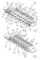
- Figure 1
- shows a top view of a protection device for a contact strip of a telecommunication distribution device, the protection device comprising a printed circuit board, arresters, a housing and grounding springs;
- Figure 2
- shows a bottom view of the protection device of
Figure 1 with the housing and grounding springs being removed; - Figure 3
- shows a top view of the printed circuit board of the protection device of
Figure 1 ; and - Figure 4
- shows a bottom view of the printed circuit board of
Figure 3 . - The present patent application relates to a contact strip of a telecommunication distribution device like a main distribution frame (MDF) block and to a telecommunication distribution device comprising such a protection device.
- A
protection device 10 comprises aprinted circuit board 11 and a plurality ofarresters 12 mounted on the printedcircuit board 11. In the illustrated embodiment, thearresters 12 are gas discharge tubes. Thearresters 12 are mounted on abottom side 13 of the printedcircuit board 11 and are covered by a housing 14. The housing 14 is preferably made from a plastic material. - The printed
circuit board 11 providescontact blades 15 thorough which theprotection device 10 is connectable to contact springs of the contact strip. Thecontact blades 15 of the printedcircuit board 11 are arranged side-by-side as a plurality ofcontact blade pairs 16. - In the shown embodiment, the printed
circuit board 11 comprises sixteencontact blades 15 arranged as eightcontact blade pairs 16. Thecontact blades 15 of eachcontact blade pair 16 are connectable with contact springs of contact spring pairs of the contact strip. - To each
contact blade pair 16 there is assigned anarrester 12 in such a way that therespective arrester 12 is electrically connected with thecontact blades 15 of the respectivecontact blade pair 16 by electricalconductive paths - The electrical
conductive paths circuit board 11. The electricalconductive paths bottom side 13 of theprinted circuit board 11. In the region of thecontact blades 15, the electricalconductive paths top side 26 of the printedcircuit board 11. Segments of the electricalconductive paths top side 26 of thecontact blades 15 contact segments of theconductive paths bottom side 13 of thecontact blades 15 by throughhole connections 28 extending through the printedcircuit board 11 between thebottom side 13 and thetop side 26 of the printedcircuit board 11. - The printed
circuit board 11 further includes throughholes lead wires arresters 12. The electricalconductive paths contact blades 15 and first and second throughholes second lead wires arresters 12. Each of the electricalconductive paths 23 extend between a first throughhole 17 and afirst contact blade 15 of the respectivecontact blade pair 16, and each of the electricalconductive paths 24 extend between the second throughhole 18 and asecond contact blade 15 of the respectivecontact blade pair 16. - The electrical
conductive paths contact blade pair 16 are in electrical contact with each other through thearrester 12 assigned to acontact blade pair 16 when the first andsecond lead wires respective arrester 12 are accommodated within the first and second throughholes - Each
arrester 12 comprises in addition to the first andsecond lead wires 20, 21 athird lead wire 22 that is electrically connected to agrounding layer 25 of the printedcircuit board 11. Thethird lead wire 22 of eacharrester 12 is accommodated by a third throughhole 19 of the printedcircuit board 11. Thegrounding layer 25 is located on thetop side 26 of the printedcircuit board 11. - The
lead wires arresters 12 are soldered to the printedcircuit board 11 in the region of the throughholes holes - On both sides of the
protection device 10grounding springs 27 are mounted to the printedcircuit board 11 so that the same are in electrical contact with thegrounding layer 25. When theprotection device 10 is accommodated in a mounting frame of a MDF block thegrounding springs 27 provide an electrically conductive path between thegrounding layer 25 of theprotection device 10 and the mounting frame of the MDF block. - The
grounding springs 27 are mounted to the printedcircuit board 11 by fastening means such asrivets 31, wherein thegrounding springs 27 are in electrical contact with thegrounding layer 25. Therivets 31 are further used to mount the housing 14 to the printedcircuit board 11. - At least the first and
second lead wires arrester 12 are bent in such a way that bent ends of thelead wires arresters 12 extend on onetop side 26 of the printedcircuit board 11 in parallel to a plane defined by the printedcircuit board 11. - Even if
arresters 12 become de-soldered, the bent ends of thelead wires arresters 12 at the printedcircuit board 11 so that thearresters 12 cannot come into contact with the housing 14, thereby preventing thearresters 12 from melting through the plastic housing 14. - It is also possible that the
third lead wires 22 of thearresters 12 comprise such bent ends. - The bent ends of the
bent lead wires arresters 12 run in the region of thetop side 26 of the printedcircuit board 11 in parallel to a plane defined by the printedcircuit board 11. The bent end of eachbent lead wire zone 29 provided on thetop side 26 of the printedcircuit board 11. The contactingzones 29 are positioned in the same plane as thegrounding layer 25. The first and second throughholes zone 29 offset from the center of the respective contactingzone 29. - Each of the contacting
zones 29 is separated from thegrounding layer 25 by an insulatingzone 30 surrounding the respective contactingzone 29. - The through holes 17, 18 provide a through contact between the two sides of the printed
circuit board 11, namely between the electricalconductive paths bottom side 13 of the printedcircuit board 11 and the contactingzones 29 provided on thetop side 16 of the printedcircuit board 11. - The through holes 19 provide also a through contact between the two sides of the printed
circuit board 11, namely from thebottom side 13 of the printedcircuit board 11 togrounding layer 25 provided on thetop side 16 of the printedcircuit board 11. - Each contacting
zone 29 has a surface between 5 mm2 and 12 mm2, preferably a surface between 5 mm2 and 9 mm2. This ensures a good electrical contact of the bend ends of thebent lead wires zone 29 and minimizes the risk of de-soldering thearresters 12. - Each insulating
zone 30 surrounding the respective contactingzone 29 has a width between 0.8 mm and 2 mm, preferably a width between 1 mm and 1.5 mm. Each insulatingsection zone 30 has a surface between 10 mm2 and 60 mm2, preferably a surface between 20 mm2 and 50 mm2. This ensures a good electrical insulation between of each contactingzone 29 and thegrounding layer 25. - The
grounding layer 25 has a surface between 1000 mm2 and 2400 mm2, preferably a surface between 1000 mm2 and 1800 mm2. This minimizes the risk of overheating of the printedcircuit board 11 even under high electrical current flows. Thegrounding layer 25 can effectively distribute heat dissipation of thearresters 12. - A contacting area between the grounding
layer 25 and each of the grounding springs has a surface between 100 mm2 and 200 mm2. - The
grounding layer 25, the contactingzones 29 and the electricalconductive paths -
Figure 2 shows that fail-safe elements 32 are assigned to thearresters 12. The fail fail-safe elements 32 are provided by foil elements. The foil elements begin to melt at temperatures of greater than 260 °C. Once anarrester 12 is shorted by fail-safe element 32, the electrical current is flowing through thearrester 12 to theground layer 25. - The
protection device 10 according to the present disclosure is capable to pass the power cross test at its highest severity. When running the a power cross test, a distribution device including a protection device is applied to the mains power of 230 V, 50 Hz for a defined period of time of 15 minutes. The test severity can be different and is defined by a test resistor, where the highest severity is when using a 10 Ω test resistor. This test results in an electrical current flow of 23 Amp (A) perlead wire arrester 12. - Even at such conditions the
protection device 10 according to the present disclosure reduces the overheating risk of the printedcircuit board 11. Accordingly, the risk of de-soldering of thearresters 12 from the printedcircuit board PCB 11 is also reduced. - If the
arresters 12 should become de-soldered, the bent ends of thebent lead wires arresters 12 at the printedcircuit board 11 so that the arresters cannot come into contact with a plastic housing 14 covering thearresters 12, thereby preventing thearresters 12 from melting through the plastic housing 14. - As discussed above, the
bent lead wires arresters 12 fix thearresters 12 properly to the solder side of the printedcircuit board 11 even though if the solder is melted. The contactingzones 29 ensure a good electrical contact of thelead wires zones 29 and ensure that molten solder won't run downlead wires grounding layer 25 distributes a lot of the heat power emitting from thearresters 12. The heat sink provided by thegrounding layer 25 supports operation of thedevice 10 by reducing the temperature of the printedcircuit board 11. - The
protection device 10 according to the present disclosure can be designed as a so-called overvoltage protection device or a so-called overvoltage and overcurrent protection device. An overvoltage and overcurrent protection device comprises in addition to thearresters 12 PTC (positive temperature coefficient) elements acting as current-dependent switches. - The present disclosure further relates to a telecommunication distribution device like to an MDF block. Such a telecommunication distribution device comprises a mounting frame, a plurality of contact strips accommodated in the mounting frame, a plurality of wire guides accommodated in the mounting frame and a plurality of protection devices accommodated in the mounting frame, wherein each protection device is connected with a contact strip, and wherein at least one protection device is designed as discussed above.
-
10 protection device 11 printed circuit board 12 arrester 13 bottom side 14 housing 15 contact blade 16 contact blade pair 17 through hole 18 through hole 19 through hole 20 lead wire 21 lead wire 22 lead wire 23 electrical conductive path 24 electrical conductive path 25 grounding layer 26 top side 27 grounding spring 28 through hole connection 29 contacting zone 30 insulating zone 31 rivet 32 fail-safe element
Claims (14)
- A protection device (10) for a contact strip of a telecommunication distribution device comprising a printed circuit board (11) and a plurality of arresters (12) mounted on the printed circuit board (11),
wherein the printed circuit board (11) provides contact blades (15) through which the protection device (10) is connectable to contact springs of the contact strip, the contact blades (15) being arranged side-by-side as a plurality of contact blade pairs (16);
wherein the printed circuit board (11) provides through holes (17, 18, 19) for receiving lead wires (20, 21, 22) of the arresters (12);
wherein to each contact blade pair (16) there is assigned an arrester (12) in such a way that the respective arrester (12) is in electrical contact with the contact blades (15) of the respective contact blade pair (16),
characterized in that
at least two lead wires (20, 21) of each arrester (12) are bent in such a way that bent ends of the bent lead wires (20, 21) of the arresters (12) extend on one side of the printed circuit board (11) in parallel to a plane defined by the printed circuit board (11). - The protection device of claim 1, characterized in that electrical conductive paths (23, 24) provided by the printed circuit board (11) extend between the contact blades (15) and first and second through holes (17, 18) for receiving first and second lead wires (20, 21) of the arresters, wherein the electrical conductive paths (23, 24) being assigned to a contact blade pair (16) are in electrical contact with each other when the first and second lead wires (20, 21) of the arrester (12) being assigned to said contact blade pair (16) are accommodated within the first and second through holes (17, 18).
- The protection device of claim 2, characterized in that the electrical conductive paths (23, 24) extending between the contact blades (15) and first and second through holes (17, 18) are located on a first side, preferably on a bottom side (13), of the printed circuit board (11).
- The protection device of claim 3, characterized in that the bent ends of the bent lead wires (20, 21) of the arresters (12) extend on a second opposite side, preferably on a top side (26), of the printed circuit board (11) in parallel to a plane defined by the printed circuit board (11).
- The protection device of one of claims 2 to 4, characterized in that only in the region of the contact blades (15) the electrical conductive paths (23, 24) extending between the contact blades (15) and first and second through holes (17, 18) are located on both sides (13, 16) of the printed circuit board (11), namely in such a way that sections of the conductive paths (23, 24) running on the opposite sides of the contact blades (15) are connected by though hole connections (28).
- The protection device of one of claims 1 to 5, characterized in that each arrester (12) comprises at least three lead wires (20, 21, 22), namely first and second lead wires (20, 21) being electrically connected with the contact blades (15) of the respective contact blade pair (16) and a third lead wire (22) being electrically connected to a grounding layer (25) of the printed circuit board (11), wherein at least the first and second lead wires (20, 21) have bent ends.
- The protection device of claim 6, characterized in that electrical conductive paths (23, 24) extending between the contact blades (15) and first and second through holes (17, 18) for receiving the first and second lead wires (20, 21) of the arresters (12) are located on a bottom side (13) of the printed circuit board (11) while the grounding layer (25) is located on a top side (26) of the printed circuit board (11).
- The protection device of claim 7, characterized in that the bent end of each bent lead wire (20, 21) is in electrical contact each with a contacting zone (29) provided on the top side (26) of the printed circuit board (11), wherein each of the contacting zones (29) is separated from the grounding layer (25) by an insulating zone (30) surrounding the respective contacting zone (29).
- The protection device of claim 8, characterized in that each contacting zone (29) has a surface between 5 mm2 and 12 mm2, preferably between 5 mm2 and 9 mm2.
- The protection device of claim 8 or 9, characterized in that each insulating zone (30) surrounding the respective contacting zone (29) has a width between 0.8 mm and 2 mm, preferably between 1,0 mm and 1,5 mm.
- The protection device of one of claims 8 to 10, characterized in that each insulating section zone (30) has a surface between 10 mm2 and 60 mm2, preferably between 20 mm2 and 50 mm2.
- The protection device of one of claims 6 to 11, characterized in that the grounding layer (25) has a surface between 1000 mm2 and 2400 mm2, preferably between 1000 mm2 and 1800 mm2.
- The protection device of one of claims 8 to 12, characterized in that grounding layer (25), the contacting zones (29) and the electrical conductive paths (23, 24) are preferably made from copper having a thickness between 100 µm and 150 µm, preferably between 120 µm and 135 µm.
- A telecommunication distribution device, comprising
a mounting frame,
a plurality of contact strips accommodated in the mounting frame,
a plurality of protection devices accommodated in the mounting frame, each protection device being connected with a contact strip,
characterized in that
at least one protection device is provided by protection device of one of claims 1 to 13.
Priority Applications (1)
| Application Number | Priority Date | Filing Date | Title |
|---|---|---|---|
| EP13158429.4A EP2775732B1 (en) | 2013-03-08 | 2013-03-08 | Protection device for a contact strip of a distribution device |
Applications Claiming Priority (1)
| Application Number | Priority Date | Filing Date | Title |
|---|---|---|---|
| EP13158429.4A EP2775732B1 (en) | 2013-03-08 | 2013-03-08 | Protection device for a contact strip of a distribution device |
Publications (2)
| Publication Number | Publication Date |
|---|---|
| EP2775732A1 true EP2775732A1 (en) | 2014-09-10 |
| EP2775732B1 EP2775732B1 (en) | 2016-02-03 |
Family
ID=47900692
Family Applications (1)
| Application Number | Title | Priority Date | Filing Date |
|---|---|---|---|
| EP13158429.4A Not-in-force EP2775732B1 (en) | 2013-03-08 | 2013-03-08 | Protection device for a contact strip of a distribution device |
Country Status (1)
| Country | Link |
|---|---|
| EP (1) | EP2775732B1 (en) |
Cited By (7)
| Publication number | Priority date | Publication date | Assignee | Title |
|---|---|---|---|---|
| WO2017212451A1 (en) * | 2016-06-10 | 2017-12-14 | Te Connectivity Corporation | Electrical contact pad for electrically contacting a connector |
| CN107995782A (en) * | 2017-12-05 | 2018-05-04 | 晶晨半导体(上海)股份有限公司 | A PCB board that optimizes the ground plane based on the internal wiring of the CPU |
| US9997868B1 (en) | 2017-07-24 | 2018-06-12 | Te Connectivity Corporation | Electrical connector with improved impedance characteristics |
| CN108811317A (en) * | 2018-07-03 | 2018-11-13 | 北京华悦龙驰科技有限公司 | A kind of via pad structure, a kind of circuit board connection type and a kind of circuit board |
| US10263352B2 (en) | 2016-06-10 | 2019-04-16 | Te Connectivity Corporation | Electrical contact pad for electrically contacting a connector |
| US10320099B2 (en) | 2016-06-10 | 2019-06-11 | Te Connectivity Corporation | Connector with asymmetric base section |
| WO2021237897A1 (en) * | 2020-05-27 | 2021-12-02 | 深圳桑椹电子商务有限公司 | Manufacturing method and structure of led substrate |
Citations (3)
| Publication number | Priority date | Publication date | Assignee | Title |
|---|---|---|---|---|
| US4331839A (en) * | 1980-12-12 | 1982-05-25 | Reliable Electric Company | Telephone distribution frame connector assembly |
| EP1983809A2 (en) * | 2007-04-19 | 2008-10-22 | Yazaki Corporation | Printed wiring board |
| US20100285693A1 (en) * | 2006-05-19 | 2010-11-11 | Adc Gmbh | Overvoltage protection magazine |
-
2013
- 2013-03-08 EP EP13158429.4A patent/EP2775732B1/en not_active Not-in-force
Patent Citations (3)
| Publication number | Priority date | Publication date | Assignee | Title |
|---|---|---|---|---|
| US4331839A (en) * | 1980-12-12 | 1982-05-25 | Reliable Electric Company | Telephone distribution frame connector assembly |
| US20100285693A1 (en) * | 2006-05-19 | 2010-11-11 | Adc Gmbh | Overvoltage protection magazine |
| EP1983809A2 (en) * | 2007-04-19 | 2008-10-22 | Yazaki Corporation | Printed wiring board |
Cited By (9)
| Publication number | Priority date | Publication date | Assignee | Title |
|---|---|---|---|---|
| WO2017212451A1 (en) * | 2016-06-10 | 2017-12-14 | Te Connectivity Corporation | Electrical contact pad for electrically contacting a connector |
| US10128597B2 (en) | 2016-06-10 | 2018-11-13 | Te Connectivity Corporation | Electrical contact pad for electrically contacting a connector |
| US10263352B2 (en) | 2016-06-10 | 2019-04-16 | Te Connectivity Corporation | Electrical contact pad for electrically contacting a connector |
| US10320099B2 (en) | 2016-06-10 | 2019-06-11 | Te Connectivity Corporation | Connector with asymmetric base section |
| US9997868B1 (en) | 2017-07-24 | 2018-06-12 | Te Connectivity Corporation | Electrical connector with improved impedance characteristics |
| CN107995782A (en) * | 2017-12-05 | 2018-05-04 | 晶晨半导体(上海)股份有限公司 | A PCB board that optimizes the ground plane based on the internal wiring of the CPU |
| CN107995782B (en) * | 2017-12-05 | 2020-06-09 | 晶晨半导体(上海)股份有限公司 | PCB (printed circuit board) for optimizing ground plane based on internal wiring of CPU (central processing unit) |
| CN108811317A (en) * | 2018-07-03 | 2018-11-13 | 北京华悦龙驰科技有限公司 | A kind of via pad structure, a kind of circuit board connection type and a kind of circuit board |
| WO2021237897A1 (en) * | 2020-05-27 | 2021-12-02 | 深圳桑椹电子商务有限公司 | Manufacturing method and structure of led substrate |
Also Published As
| Publication number | Publication date |
|---|---|
| EP2775732B1 (en) | 2016-02-03 |
Similar Documents
| Publication | Publication Date | Title |
|---|---|---|
| EP2775732B1 (en) | Protection device for a contact strip of a distribution device | |
| US3978443A (en) | Fusible resistor | |
| TW201230116A (en) | Compact transient voltage surge suppression device | |
| WO2007105066A1 (en) | Device for overvoltage protection | |
| JP6739642B2 (en) | Substrate and battery for electrically fixed connection of battery cells | |
| JP6694551B2 (en) | Board for connecting battery cells | |
| JP4708338B2 (en) | Telecommunications circuit protection device | |
| US9450349B1 (en) | Power socket with over-current protection | |
| EP0395231B1 (en) | Protective arrangement for telecommunications line interface circuit | |
| US9893601B2 (en) | Brush plate | |
| CN110859051A (en) | Thermally protected metal oxide varistor | |
| CN222440487U (en) | A thermal overload structure and thermal overload relay | |
| US20130314201A1 (en) | Over-current protection fuses | |
| CA3163239C (en) | Semiconductor device, printed circuit board (pcb), and method of interfacing control pin (gate pin) of a power semiconductor device (mosfet) to a printed circuit board (pcb) in a battery management system (bms) | |
| CN220569487U (en) | Metal oxide varistor comprising insulating disc | |
| CN222814237U (en) | Surge protection device | |
| KR101025712B1 (en) | PTC device | |
| EP2409305B1 (en) | Resistor device, method for providing the same and load distribution system | |
| US10779397B1 (en) | Circuit board structure and layout structure thereof | |
| KR200485742Y1 (en) | Apparatus preventing thermal runway for varistor | |
| EP0507465A2 (en) | A resistor capable of acting as a circuit breaker | |
| US20080157917A1 (en) | Method to increase capacity of a passive element to inrush current | |
| EP2378527A2 (en) | Device for overvoltage protection | |
| DE19720610A1 (en) | Overtemperature protection device | |
| KR20110008077U (en) | Resistor and circuit board having the same |
Legal Events
| Date | Code | Title | Description |
|---|---|---|---|
| PUAI | Public reference made under article 153(3) epc to a published international application that has entered the european phase |
Free format text: ORIGINAL CODE: 0009012 |
|
| 17P | Request for examination filed |
Effective date: 20130308 |
|
| AK | Designated contracting states |
Kind code of ref document: A1 Designated state(s): AL AT BE BG CH CY CZ DE DK EE ES FI FR GB GR HR HU IE IS IT LI LT LU LV MC MK MT NL NO PL PT RO RS SE SI SK SM TR |
|
| AX | Request for extension of the european patent |
Extension state: BA ME |
|
| R17P | Request for examination filed (corrected) |
Effective date: 20150226 |
|
| RBV | Designated contracting states (corrected) |
Designated state(s): AL AT BE BG CH CY CZ DE DK EE ES FI FR GB GR HR HU IE IS IT LI LT LU LV MC MK MT NL NO PL PT RO RS SE SI SK SM TR |
|
| GRAP | Despatch of communication of intention to grant a patent |
Free format text: ORIGINAL CODE: EPIDOSNIGR1 |
|
| RIC1 | Information provided on ipc code assigned before grant |
Ipc: H05K 3/30 20060101ALI20150611BHEP Ipc: H04Q 1/14 20060101AFI20150611BHEP |
|
| INTG | Intention to grant announced |
Effective date: 20150630 |
|
| GRAS | Grant fee paid |
Free format text: ORIGINAL CODE: EPIDOSNIGR3 |
|
| GRAP | Despatch of communication of intention to grant a patent |
Free format text: ORIGINAL CODE: EPIDOSNIGR1 |
|
| INTG | Intention to grant announced |
Effective date: 20151113 |
|
| GRAA | (expected) grant |
Free format text: ORIGINAL CODE: 0009210 |
|
| AK | Designated contracting states |
Kind code of ref document: B1 Designated state(s): AL AT BE BG CH CY CZ DE DK EE ES FI FR GB GR HR HU IE IS IT LI LT LU LV MC MK MT NL NO PL PT RO RS SE SI SK SM TR |
|
| REG | Reference to a national code |
Ref country code: GB Ref legal event code: FG4D |
|
| REG | Reference to a national code |
Ref country code: AT Ref legal event code: REF Ref document number: 774143 Country of ref document: AT Kind code of ref document: T Effective date: 20160215 Ref country code: CH Ref legal event code: EP |
|
| REG | Reference to a national code |
Ref country code: IE Ref legal event code: FG4D |
|
| REG | Reference to a national code |
Ref country code: DE Ref legal event code: R096 Ref document number: 602013004844 Country of ref document: DE |
|
| REG | Reference to a national code |
Ref country code: FR Ref legal event code: PLFP Year of fee payment: 4 |
|
| REG | Reference to a national code |
Ref country code: LT Ref legal event code: MG4D Ref country code: NL Ref legal event code: MP Effective date: 20160203 |
|
| REG | Reference to a national code |
Ref country code: AT Ref legal event code: MK05 Ref document number: 774143 Country of ref document: AT Kind code of ref document: T Effective date: 20160203 |
|
| PG25 | Lapsed in a contracting state [announced via postgrant information from national office to epo] |
Ref country code: FI Free format text: LAPSE BECAUSE OF FAILURE TO SUBMIT A TRANSLATION OF THE DESCRIPTION OR TO PAY THE FEE WITHIN THE PRESCRIBED TIME-LIMIT Effective date: 20160203 Ref country code: NO Free format text: LAPSE BECAUSE OF FAILURE TO SUBMIT A TRANSLATION OF THE DESCRIPTION OR TO PAY THE FEE WITHIN THE PRESCRIBED TIME-LIMIT Effective date: 20160503 Ref country code: HR Free format text: LAPSE BECAUSE OF FAILURE TO SUBMIT A TRANSLATION OF THE DESCRIPTION OR TO PAY THE FEE WITHIN THE PRESCRIBED TIME-LIMIT Effective date: 20160203 Ref country code: ES Free format text: LAPSE BECAUSE OF FAILURE TO SUBMIT A TRANSLATION OF THE DESCRIPTION OR TO PAY THE FEE WITHIN THE PRESCRIBED TIME-LIMIT Effective date: 20160203 Ref country code: IT Free format text: LAPSE BECAUSE OF FAILURE TO SUBMIT A TRANSLATION OF THE DESCRIPTION OR TO PAY THE FEE WITHIN THE PRESCRIBED TIME-LIMIT Effective date: 20160203 Ref country code: GR Free format text: LAPSE BECAUSE OF FAILURE TO SUBMIT A TRANSLATION OF THE DESCRIPTION OR TO PAY THE FEE WITHIN THE PRESCRIBED TIME-LIMIT Effective date: 20160504 |
|
| PG25 | Lapsed in a contracting state [announced via postgrant information from national office to epo] |
Ref country code: BE Free format text: LAPSE BECAUSE OF NON-PAYMENT OF DUE FEES Effective date: 20160331 Ref country code: LT Free format text: LAPSE BECAUSE OF FAILURE TO SUBMIT A TRANSLATION OF THE DESCRIPTION OR TO PAY THE FEE WITHIN THE PRESCRIBED TIME-LIMIT Effective date: 20160203 Ref country code: PT Free format text: LAPSE BECAUSE OF FAILURE TO SUBMIT A TRANSLATION OF THE DESCRIPTION OR TO PAY THE FEE WITHIN THE PRESCRIBED TIME-LIMIT Effective date: 20160603 Ref country code: LV Free format text: LAPSE BECAUSE OF FAILURE TO SUBMIT A TRANSLATION OF THE DESCRIPTION OR TO PAY THE FEE WITHIN THE PRESCRIBED TIME-LIMIT Effective date: 20160203 Ref country code: RS Free format text: LAPSE BECAUSE OF FAILURE TO SUBMIT A TRANSLATION OF THE DESCRIPTION OR TO PAY THE FEE WITHIN THE PRESCRIBED TIME-LIMIT Effective date: 20160203 Ref country code: IS Free format text: LAPSE BECAUSE OF FAILURE TO SUBMIT A TRANSLATION OF THE DESCRIPTION OR TO PAY THE FEE WITHIN THE PRESCRIBED TIME-LIMIT Effective date: 20160603 Ref country code: NL Free format text: LAPSE BECAUSE OF FAILURE TO SUBMIT A TRANSLATION OF THE DESCRIPTION OR TO PAY THE FEE WITHIN THE PRESCRIBED TIME-LIMIT Effective date: 20160203 Ref country code: PL Free format text: LAPSE BECAUSE OF FAILURE TO SUBMIT A TRANSLATION OF THE DESCRIPTION OR TO PAY THE FEE WITHIN THE PRESCRIBED TIME-LIMIT Effective date: 20160203 Ref country code: AT Free format text: LAPSE BECAUSE OF FAILURE TO SUBMIT A TRANSLATION OF THE DESCRIPTION OR TO PAY THE FEE WITHIN THE PRESCRIBED TIME-LIMIT Effective date: 20160203 Ref country code: SE Free format text: LAPSE BECAUSE OF FAILURE TO SUBMIT A TRANSLATION OF THE DESCRIPTION OR TO PAY THE FEE WITHIN THE PRESCRIBED TIME-LIMIT Effective date: 20160203 |
|
| PG25 | Lapsed in a contracting state [announced via postgrant information from national office to epo] |
Ref country code: DK Free format text: LAPSE BECAUSE OF FAILURE TO SUBMIT A TRANSLATION OF THE DESCRIPTION OR TO PAY THE FEE WITHIN THE PRESCRIBED TIME-LIMIT Effective date: 20160203 Ref country code: EE Free format text: LAPSE BECAUSE OF FAILURE TO SUBMIT A TRANSLATION OF THE DESCRIPTION OR TO PAY THE FEE WITHIN THE PRESCRIBED TIME-LIMIT Effective date: 20160203 |
|
| REG | Reference to a national code |
Ref country code: CH Ref legal event code: PL |
|
| REG | Reference to a national code |
Ref country code: DE Ref legal event code: R097 Ref document number: 602013004844 Country of ref document: DE |
|
| PG25 | Lapsed in a contracting state [announced via postgrant information from national office to epo] |
Ref country code: SK Free format text: LAPSE BECAUSE OF FAILURE TO SUBMIT A TRANSLATION OF THE DESCRIPTION OR TO PAY THE FEE WITHIN THE PRESCRIBED TIME-LIMIT Effective date: 20160203 Ref country code: RO Free format text: LAPSE BECAUSE OF FAILURE TO SUBMIT A TRANSLATION OF THE DESCRIPTION OR TO PAY THE FEE WITHIN THE PRESCRIBED TIME-LIMIT Effective date: 20160203 Ref country code: SM Free format text: LAPSE BECAUSE OF FAILURE TO SUBMIT A TRANSLATION OF THE DESCRIPTION OR TO PAY THE FEE WITHIN THE PRESCRIBED TIME-LIMIT Effective date: 20160203 Ref country code: CZ Free format text: LAPSE BECAUSE OF FAILURE TO SUBMIT A TRANSLATION OF THE DESCRIPTION OR TO PAY THE FEE WITHIN THE PRESCRIBED TIME-LIMIT Effective date: 20160203 |
|
| PLBE | No opposition filed within time limit |
Free format text: ORIGINAL CODE: 0009261 |
|
| STAA | Information on the status of an ep patent application or granted ep patent |
Free format text: STATUS: NO OPPOSITION FILED WITHIN TIME LIMIT |
|
| REG | Reference to a national code |
Ref country code: IE Ref legal event code: MM4A |
|
| PG25 | Lapsed in a contracting state [announced via postgrant information from national office to epo] |
Ref country code: BE Free format text: LAPSE BECAUSE OF FAILURE TO SUBMIT A TRANSLATION OF THE DESCRIPTION OR TO PAY THE FEE WITHIN THE PRESCRIBED TIME-LIMIT Effective date: 20160203 |
|
| 26N | No opposition filed |
Effective date: 20161104 |
|
| PG25 | Lapsed in a contracting state [announced via postgrant information from national office to epo] |
Ref country code: LI Free format text: LAPSE BECAUSE OF NON-PAYMENT OF DUE FEES Effective date: 20160331 Ref country code: CH Free format text: LAPSE BECAUSE OF NON-PAYMENT OF DUE FEES Effective date: 20160331 Ref country code: IE Free format text: LAPSE BECAUSE OF NON-PAYMENT OF DUE FEES Effective date: 20160308 |
|
| PG25 | Lapsed in a contracting state [announced via postgrant information from national office to epo] |
Ref country code: BG Free format text: LAPSE BECAUSE OF FAILURE TO SUBMIT A TRANSLATION OF THE DESCRIPTION OR TO PAY THE FEE WITHIN THE PRESCRIBED TIME-LIMIT Effective date: 20160503 Ref country code: SI Free format text: LAPSE BECAUSE OF FAILURE TO SUBMIT A TRANSLATION OF THE DESCRIPTION OR TO PAY THE FEE WITHIN THE PRESCRIBED TIME-LIMIT Effective date: 20160203 |
|
| REG | Reference to a national code |
Ref country code: FR Ref legal event code: PLFP Year of fee payment: 5 |
|
| PG25 | Lapsed in a contracting state [announced via postgrant information from national office to epo] |
Ref country code: MT Free format text: LAPSE BECAUSE OF FAILURE TO SUBMIT A TRANSLATION OF THE DESCRIPTION OR TO PAY THE FEE WITHIN THE PRESCRIBED TIME-LIMIT Effective date: 20160203 |
|
| REG | Reference to a national code |
Ref country code: FR Ref legal event code: PLFP Year of fee payment: 6 |
|
| PG25 | Lapsed in a contracting state [announced via postgrant information from national office to epo] |
Ref country code: HU Free format text: LAPSE BECAUSE OF FAILURE TO SUBMIT A TRANSLATION OF THE DESCRIPTION OR TO PAY THE FEE WITHIN THE PRESCRIBED TIME-LIMIT; INVALID AB INITIO Effective date: 20130308 |
|
| PG25 | Lapsed in a contracting state [announced via postgrant information from national office to epo] |
Ref country code: MT Free format text: LAPSE BECAUSE OF FAILURE TO SUBMIT A TRANSLATION OF THE DESCRIPTION OR TO PAY THE FEE WITHIN THE PRESCRIBED TIME-LIMIT Effective date: 20160331 Ref country code: MC Free format text: LAPSE BECAUSE OF FAILURE TO SUBMIT A TRANSLATION OF THE DESCRIPTION OR TO PAY THE FEE WITHIN THE PRESCRIBED TIME-LIMIT Effective date: 20160203 Ref country code: TR Free format text: LAPSE BECAUSE OF FAILURE TO SUBMIT A TRANSLATION OF THE DESCRIPTION OR TO PAY THE FEE WITHIN THE PRESCRIBED TIME-LIMIT Effective date: 20160203 Ref country code: MK Free format text: LAPSE BECAUSE OF FAILURE TO SUBMIT A TRANSLATION OF THE DESCRIPTION OR TO PAY THE FEE WITHIN THE PRESCRIBED TIME-LIMIT Effective date: 20160203 Ref country code: CY Free format text: LAPSE BECAUSE OF FAILURE TO SUBMIT A TRANSLATION OF THE DESCRIPTION OR TO PAY THE FEE WITHIN THE PRESCRIBED TIME-LIMIT Effective date: 20160203 Ref country code: LU Free format text: LAPSE BECAUSE OF NON-PAYMENT OF DUE FEES Effective date: 20160308 |
|
| PG25 | Lapsed in a contracting state [announced via postgrant information from national office to epo] |
Ref country code: AL Free format text: LAPSE BECAUSE OF FAILURE TO SUBMIT A TRANSLATION OF THE DESCRIPTION OR TO PAY THE FEE WITHIN THE PRESCRIBED TIME-LIMIT Effective date: 20160203 |
|
| PGFP | Annual fee paid to national office [announced via postgrant information from national office to epo] |
Ref country code: GB Payment date: 20190227 Year of fee payment: 7 Ref country code: DE Payment date: 20190215 Year of fee payment: 7 |
|
| PGFP | Annual fee paid to national office [announced via postgrant information from national office to epo] |
Ref country code: FR Payment date: 20190220 Year of fee payment: 7 |
|
| REG | Reference to a national code |
Ref country code: DE Ref legal event code: R119 Ref document number: 602013004844 Country of ref document: DE |
|
| PG25 | Lapsed in a contracting state [announced via postgrant information from national office to epo] |
Ref country code: FR Free format text: LAPSE BECAUSE OF NON-PAYMENT OF DUE FEES Effective date: 20200331 Ref country code: DE Free format text: LAPSE BECAUSE OF NON-PAYMENT OF DUE FEES Effective date: 20201001 |
|
| GBPC | Gb: european patent ceased through non-payment of renewal fee |
Effective date: 20200308 |
|
| PG25 | Lapsed in a contracting state [announced via postgrant information from national office to epo] |
Ref country code: GB Free format text: LAPSE BECAUSE OF NON-PAYMENT OF DUE FEES Effective date: 20200308 |