EP2775621B1 - A Dickson charge pump circuit - Google Patents
A Dickson charge pump circuit Download PDFInfo
- Publication number
- EP2775621B1 EP2775621B1 EP13158227.2A EP13158227A EP2775621B1 EP 2775621 B1 EP2775621 B1 EP 2775621B1 EP 13158227 A EP13158227 A EP 13158227A EP 2775621 B1 EP2775621 B1 EP 2775621B1
- Authority
- EP
- European Patent Office
- Prior art keywords
- switch
- high side
- charge pump
- pumping stage
- pump circuit
- Prior art date
- Legal status (The legal status is an assumption and is not a legal conclusion. Google has not performed a legal analysis and makes no representation as to the accuracy of the status listed.)
- Active
Links
Images




Classifications
-
- H—ELECTRICITY
- H03—ELECTRONIC CIRCUITRY
- H03K—PULSE TECHNIQUE
- H03K17/00—Electronic switching or gating, i.e. not by contact-making and –breaking
- H03K17/06—Modifications for ensuring a fully conducting state
- H03K17/063—Modifications for ensuring a fully conducting state in field-effect transistor switches
-
- H—ELECTRICITY
- H02—GENERATION; CONVERSION OR DISTRIBUTION OF ELECTRIC POWER
- H02M—APPARATUS FOR CONVERSION BETWEEN AC AND AC, BETWEEN AC AND DC, OR BETWEEN DC AND DC, AND FOR USE WITH MAINS OR SIMILAR POWER SUPPLY SYSTEMS; CONVERSION OF DC OR AC INPUT POWER INTO SURGE OUTPUT POWER; CONTROL OR REGULATION THEREOF
- H02M3/00—Conversion of DC power input into DC power output
- H02M3/02—Conversion of DC power input into DC power output without intermediate conversion into AC
- H02M3/04—Conversion of DC power input into DC power output without intermediate conversion into AC by static converters
- H02M3/06—Conversion of DC power input into DC power output without intermediate conversion into AC by static converters using resistors or capacitors, e.g. potential divider
- H02M3/07—Conversion of DC power input into DC power output without intermediate conversion into AC by static converters using resistors or capacitors, e.g. potential divider using capacitors charged and discharged alternately by semiconductor devices with control electrode, e.g. charge pumps
-
- H—ELECTRICITY
- H02—GENERATION; CONVERSION OR DISTRIBUTION OF ELECTRIC POWER
- H02M—APPARATUS FOR CONVERSION BETWEEN AC AND AC, BETWEEN AC AND DC, OR BETWEEN DC AND DC, AND FOR USE WITH MAINS OR SIMILAR POWER SUPPLY SYSTEMS; CONVERSION OF DC OR AC INPUT POWER INTO SURGE OUTPUT POWER; CONTROL OR REGULATION THEREOF
- H02M3/00—Conversion of DC power input into DC power output
- H02M3/02—Conversion of DC power input into DC power output without intermediate conversion into AC
- H02M3/04—Conversion of DC power input into DC power output without intermediate conversion into AC by static converters
- H02M3/06—Conversion of DC power input into DC power output without intermediate conversion into AC by static converters using resistors or capacitors, e.g. potential divider
- H02M3/07—Conversion of DC power input into DC power output without intermediate conversion into AC by static converters using resistors or capacitors, e.g. potential divider using capacitors charged and discharged alternately by semiconductor devices with control electrode, e.g. charge pumps
- H02M3/073—Charge pumps of the Schenkel-type
- H02M3/078—Charge pumps of the Schenkel-type with means for reducing the back bias effect, i.e. the effect which causes the threshold voltage of transistors to increase as more stages are added to the converters
-
- H—ELECTRICITY
- H03—ELECTRONIC CIRCUITRY
- H03K—PULSE TECHNIQUE
- H03K2217/00—Indexing scheme related to electronic switching or gating, i.e. not by contact-making or -breaking covered by H03K17/00
- H03K2217/0018—Special modifications or use of the back gate voltage of a FET
-
- H—ELECTRICITY
- H03—ELECTRONIC CIRCUITRY
- H03K—PULSE TECHNIQUE
- H03K2217/00—Indexing scheme related to electronic switching or gating, i.e. not by contact-making or -breaking covered by H03K17/00
- H03K2217/0063—High side switches, i.e. the higher potential [DC] or life wire [AC] being directly connected to the switch and not via the load
Definitions
- the invention relates to a high side switch comprising a Dickson charge pump circuit with increased efficiency.
- a charge pump circuit is an electronic circuit which can convert a supply voltage to a DC output voltage that can be several times higher than the supply voltage.
- Charge pump circuits are mostly made of capacitors and switches or diodes thereby allowing the integration on a silicon chip.
- a charge pump circuit uses capacitors as energy storage elements to create a voltage power source.
- a charge pump circuit uses switching elements to control the connection of voltages between the capacitors.
- a charge pump circuit can comprise several stages connected to each other via switching elements.
- the charge pump circuits are used in a wide range of applications. They can, for instance, be used as LCD or LED drivers generating high-bias voltages from a single low voltage supply such as a battery.
- Charge pump circuits can also be integrated in EEPROM and flash memory devices. Another application is the use of a charge pump circuit in a high side switch as illustrated in Fig. 1 .
- Fig. 1 shows a conventional intelligent power switch.
- These intelligent power switches or smart switches are electronic circuits that can control an electric power and are capable and rigid enough for self-protection and to protect a load and the surrounding environment.
- Smart switches are a modern form of relays but with intelligent protection functions implemented inside.
- High voltages and tens of amperes of DC currents can for instance be controlled by a vertical DMOS transistor as illustrated in Fig. 1 .
- the use of high side switches as shown in Fig. 1 is preferred. Because of a two to three times better R ON resistance of NMOS transistors than PMOS transistors at the same amount of area when integrated on a chip, the use of NMOS transistors as power switches is preferred over PMOS transistors.
- a positive gate source voltage V GS is needed. Consequently, for a high side switch, a circuit is provided that generates a supply voltage being higher than the battery voltage. To generate this high voltage, a charge pump circuit is provided within the high side switch as illustrated in Fig. 1 . For a low switch-on resistance R ON , it is important to provide a charge pump circuit with a high charge pump efficiency.
- a Dickson charge pump circuit is used.
- Fig. 2 shows a circuit diagram of a conventional Dickson charge pump circuit.
- the Dickson charge pump circuit shown in Fig. 2 can consist of a large number of identical stages each containing a diode and a capacitor C wherein the button plates of the capacitors in consecutive stages are driven by two complementary clock signals. The electric charge is transferred from one capacitor to the next capacitor at a rhythm of the applied clock signal, thus using an output voltage that can be much higher than the input voltage applied to the diode of the first stage. It is possible that a feedback control loop is added to the circuit in order to maintain the output voltage stable and independent of system parameters or load characteristics. This can be achieved by continuously adjusting a clock frequency of the charge pump circuit.
- the diode used in a conventional Dickson charge pump circuit as shown in Fig. 2 can be implemented by isolated bipolar transistors with its base and collector terminals tied together (externally) and with the parasitic devices associated to it as illustrated in Fig. 3 .
- the first disadvantage of this conventional implementation is the parasitic pnp transistor created.
- the bipolar diode opens and tries to transfer the electric charge from capacitor C1 to capacitor C2.
- the parasitic resistance R C the internal collector which acts as the base of the parasitic pnp transistor, is pulled down by the main bipolar transistor and the parasitic pnp transistor opens drawing all the electric charge from capacitor C1 and injecting the charge into the P well.
- a further disadvantage of the conventional implementation shown in Fig. 3 is that a reverse breakdown voltage of the base to emitter junction makes the diode not compatible with medium and high voltage applications. Accordingly, it has been proposed to use NMOS diode connected transistors as charge transfer devices as illustrated in Fig. 4 .
- Another disadvantage using this kind of implementation is a minimum voltage drop obtained over the diodes corresponding to the threshold voltage of these high voltage MOS transistors (i.e. about 1V).
- Another disadvantage of the conventional implementation shown in Fig. 4 is that the voltage drop varies due to the body effect because of the varying body to source voltage. This in turn lowers the overall charge pump efficiency of the charge pump circuit.
- FIG. 5 Another conventional implementation of a charge pump circuit is shown in Fig. 5 .
- This configuration was proposed by ( Jieh-Tsorng Wu, Kuen-Long Chang, "MOS Charge Pumps for Low Voltage Operation” in IEEE Journal of Solid-State Circuits, vol. 33, No. 4, April 1998 .
- the disadvantage of this implementation is that it is only suitable for low voltage applications and needs a big area when integrated on a chip.
- Document US 2013/0026829 A1 discloses an electronic circuit with an electronic switch and with a drive circuit for the electronic switch.
- FIG. 6 A further conventional implementation of a charge pump circuit is shown in Fig. 6 .
- This configuration has been proposed by Jongshin Shin, In-Young Chung, Young June Park, Hong Shick Min, "A New Charge Pump without Degradation in Threshold Voltage due to Body Effect" in IEEE Journal of Solid-State Circuits, vol. 35, No. 8, August 2000 .
- the disadvantage of this conventional implementation is that it is only compatible with low voltage technologies and also needs a big area when integrated on a chip. Further parasitic devices can disturb a correct functionality of the charge pump circuit due to bulk (substrate) switching.
- Fig. 7 shows a further conventional implementation of a charge pump circuit.
- This implementation has been proposed by Phang, K., Johns, D., "A 1V 1mW CMOS Front-End with On-Chip Dynamic Gate Biasing for a 75Mb/s Optical Receiver" in IEEE Int. Solid-State Circuits Conference, pp. 218-219, in February 2001 .
- this conventional charge pump circuit has as a disadvantage that it is only compatible with low voltage applications. There is a need to control the bulk of the transistors. This can lead to incorrect functionality of the circuit due to parasitic devices associated.
- a high side switch comprising a Dickson charge pump circuit which overcomes the above disadvantages of the conventional charge pump circuits and which provides a high charge pump efficiency.
- a Dickson charge pump circuit DCPC with increased efficiency is provided.
- Fig. 8 illustrates a basic idea underlying the present invention.
- the Dickson charge pump circuit DCPC has at least one serial connected pumping stage as illustrated in Fig. 8 which has a charge transfer switch adapted to transfer an electrical charge Q from an input of the pumping stage to the output of the respective pumping stage.
- the charge transfer switch of the pumping stage comprises a high voltage depletion NMOS transistor having a bulk connected to a floating supply voltage being lower than an input voltage applied to the input of the pumping stage.
- the above-identified problem of a pnp parasitic transistor is solved by an npn parasitic transistor associated to the high voltage depletion NMOS transistor which can be biased in such a way that this parasitic transistor is never activated, i.e. the bulk is at a lower potential than the input voltage applied to the input of the pumping stage. If, for any reason, the npn parasitic transistor shown in Fig. 8 is activated, it does not draw the electrical charge from the capacitors C but injects the charge Q into it from the N substrate. In this case, the charging of the capacitors C is done faster than without the activation of the parasitic transistor.
- V O U T V I N + N * C C + C S * V ⁇ ⁇ V D ⁇ V D ⁇ N * I O U T C + C S * f O S C ,
- the pumping stage of the Dickson charge pump circuit DCPC shown in Fig. 8 uses as a charge transfer switch a high voltage depletion NMOS transistor which has a resistance R DSON which when switched on has a low voltage drop V D . So by decreasing the voltage drop V D the efficiency of the Dickson charge pump circuit DCPC is increased, wherein the efficiency can be defined as I OUT /area of the integrated circuit at a fixed output voltage V OUT . In other words, for the same amount of area used for integration of the pumping stage mainly be occupied by the implemented capacitors C, one can draw more electrical power P from the Dickson charge pump circuit DCPC for a given output voltage V OUT .
- the Dickson charge pump circuit DCPC with increased efficiency uses a depletion NMOS transistor as a charge transfer switch. This configuration is easier to control than an implementation using for instance an enhancement NMOS transistor.
- an NMOS depletion transistor as a charge transfer switch as illustrated in Fig. 8 , the technical problem of activating a parasitic transistor that discharges the capacitors instead of charging them is overcome.
- Fig. 9 shows a circuit diagram illustrating a possible implementation of a Dickson charge pump circuit DCPC.
- a charge transfer switch is implemented by a high voltage depletion NMOS transistor having a source terminal S, a gate terminal G and a drain terminal D.
- An electrical charge Q is transferred from a first capacitor C1 via the charge transfer switch to a second capacitor C2.
- the bulk terminal B of the high voltage depletion NMOS transistor is connected to a floating supply voltage being lower than an input voltage applied to the input IN of the pumping stage.
- the driving oscillation signals OSC generated by an oscillation signal generation circuit are applied to the charge transfer capacitors C1, C2.
- a PMOS transistor P1 is connected between the source terminal S and the gate terminal G of the high voltage depletion NMOS transistor of the pumping stage. Further, an NMOS transistor N1 is connected between the floating supply voltage and the gate terminal G of the high voltage depletion NMOS transistor of the pumping stage. The gate of the PMOS transistor P1 and the gate of the NMOS transistor N1 are connected to each other and receive a driving oscillation signal OSC B generated by the oscillation signal generation circuit.
- OSC B driving oscillation signal generated by the oscillation signal generation circuit.
- the threshold voltage V TH is negative, a zero gate source voltage V GS is enough to fully turn on the charge transfer switch formed by the high voltage depletion NMOS transistor. There is no need for a higher voltage. If the gate G of the high voltage depletion NMOS transistor is pulled low enough to be under the threshold voltage, the charge transfer switch turns off. This is an advantage for the Dickson charge pump circuit, because it reduces the complexity of the circuit provided to control the gate G of the charge transfer switches.
- V GS In a conventional circuit in order to turn on an NMOS transistor, a positive gate source voltage V GS is required.
- the charge transfer switch must be on when the voltage over the capacitors is high in order to transfer electrical charge Q to the next pumping stage. Consequently, in a conventional circuit one needs to assure a positive gate source voltage V GS . This implies level shifter stages and the voltage supply is higher than the charge pump's voltage itself. Accordingly, the charge pump circuit as illustrated in Fig. 9 uses a high voltage depletion NMOS transistor to overcome these disadvantages.
- the only required control circuit is an inverter-like stage that turns on and off the high voltage depletion NMOS transistor.
- V LOW-SUP as illustrated in Fig. 9 is an internal floating supply voltage for the Dickson charge pump circuit.
- OSCA, OSCB are driving clock oscillation signals with non-overlap. If the first capacitor C1 is already charged up by the previous pumping stage, then when OSCB goes down the low voltage isolated well PMOS transistor P1 turns on and the NMOS transistor N1 turns off. The PMOS transistor P1 pulls the gate G of the high voltage depletion NMOS transistor to its source S generating a gate source voltage V GS of zero volts which is enough for the depletion NMOS transistor to fully turn on.
- the oscillation signal OSCA goes up, it charges the second capacitor C2 in a time being equal to the time constant given by the on resistance R ON of the high voltage depletion NMOS transistor and the capacitance C of the capacitor C2.
- the charge transfer switch is scaled in order to fully charge the second capacitor C2 at an operating frequency of the Dickson charge pump circuit DCPC.
- the driving oscillation signal OSCA goes up before the driving oscillation signal OSCB in order not to discharge the second capacitor C2 through the depletion back to the first capacitor C1.
- the driving oscillation signal OSCA goes down the PMOS transistor P1 turns off because the other driving oscillation signal is already down and the transistor N1 turns on assuring that the high voltage depletion NMOS transistor is off.
- Fig. 10 shows a circuit diagram of a possible embodiment of a high side switch HS-SW comprising a Dickson charge pump circuit DCPC.
- An oscillation signal generation circuit OSGC generates oscillation signals which are applied to the Dickson charge pump circuit DCPC.
- the floating supply voltage of the Dickson charge pump circuit DCPC is clamped to the input voltage applied to the input of the first pumping stage of the Dickson charge pump circuit DCPC.
- the input of the first pumping stage of the Dickson charge pump circuit DCPC is switchable by means of a supply voltage switch SW-SUP to a supply voltage V S as illustrated in Fig. 10 .
- the input of the first pumping stage of the Dickson charge pump circuit DCPC is clamped by means of a Zener diode Z to the output of a power switch PS of the high side switch HS-SW having one or several output terminals each of which can be connected to a load L.
- the power switch PS of the high side switch is a DMOS transistor driving a load L.
- the supply voltage V S applied to a supply voltage terminal of the high side switch HS-SW is provided by a battery. As illustrated in Fig. 10 , the supply voltage switch SW-SUP is adapted to switch the Dickson charge pump circuit DCPC to the supply voltage V S being equal to the battery voltage.
- This supply voltage switch SW-SUP can be formed by a MOS transistor having a gate connected to a signal input of the high side switch. As shown in Fig. 10 , at the input a driver circuit D can be provided having an output connected to the gate of the supply voltage switch SW-SUP.
- the signal input IN of the high side switch HS-SW is connected via the driver D to the gate of the supply voltage switch SW-SUP and a charging/discharging switch SW C/D being switchable between a charging current source CCS and a discharging current source DCS connected to the power switch PS as illustrated in Fig. 10 .
- Fig. 10 In the embodiment shown in Fig.
- the Dickson charge pump circuit DCPC is used in a multichannel high side switch HS-SW having several outputs or channels for different loads L. Because of the increased efficiency of the Dickson charge pump circuit DCPC, the same Dickson charge pump circuit DCPC can be used as a supply for the gate driver circuits of the main power switches PS for the different channels. In this way, the area occupied by this kind of supply circuit when integrated on a chip is minimized.
- Fig. 11 shows a possible implementation of a Dickson charge pump circuit DCPC which can be used in the high side switch HS-SW as illustrated in Fig. 10 .
- the Dickson charge pump circuit DCPC comprises two pumping stages and an output stage.
- Each pumping stage comprises a charge transfer switch implemented by a high voltage depletion transistor as illustrated in Fig. 11 .
- the bulk B of each high voltage depletion NMOS transistor is connected to a floating supply voltage V-low-sup whose potential is lower than an input voltage applied to the input of the respective pumping stage.
- a PMOS transistor P1 is connected between a source terminal S and the gate terminal G of the high voltage depletion NMOS transistor.
- an NMOS transistor N1 is connected between the floating supply voltage and the gate terminal G of the high voltage depletion NMOS transistor of the respective pumping stage.
- the gate of the PMOS transistor P1 and the gate of the NMOS transistor N1 are connected to each other and receive a driving oscillation signal generated by the oscillation signal generation circuit OSGC.
- the first driving oscillation signal OSC1 is applied to the gates of the PMOS transistor P1 and the NMOS transistor N1 of the first pumping stage.
- the second driving oscillation signal OSC2 is applied to the capacitor C1 of the first pumping stage.
- a further driving oscillation signal OSC3 is applied to the gates of the PMOS transistor P2 and the NMOS transistor N2 of the second pumping stage as well as to the capacitor C2 of the second pumping stage.
- the first oscillation signal OSC1 is logical high, the second driving oscillation signal OSC2 is also logical high but the third oscillation signal OSC3 is low.
- the first oscillation signal OSC1 can be the same as the second driving oscillation signal OSC2.
- the output voltage V1 of the first pumping stage is applied as an input voltage to the second pumping stage.
- the output voltage V2 of the second pumping stage supplies is applied via an output switch to an output capacitor C OUT having a higher capacitance than the capacitors C1 and C2 of the first and second pumping stage. Parallel to the output capacitor C OUT a Zener Z diode can be provided.
- a charge transfer switch can be implemented by a high voltage depletion NMOS transistor whose gate G is connected to a junction node between a PMOS transistor P1 and an NMOS transistor N1.
- the PMOS transistor P1 is connected between the source terminal S and the gate terminal G of the high voltage depletion NMOS transistor of the pumping stage shown in Fig. 12 .
- the NMOS transistor N1 is connected between the floating supply voltage applied at GND-CP and the gate terminal G of the high voltage depletion NMOS transistor of the pumping stage.
- the gate of the PMOS transistor P1 and the gate of the NMOS transistor N1 are connected to each other and receive a driving oscillation signal through a driving circuit as illustrated in Fig. 12 .
- the driving oscillation signal applied to the gate terminals of the transistors P1, N1 is the same as the driving oscillation signal applied to the capacitor C of the respective pumping stage.
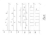
- Fig. 13 shows as a first signal diagram the current I1 flowing through the charge transfer switch implemented by the high voltage depletion NMOS transistor.
- the current I2 shown as a second diagram of Fig. 13 is the current flowing into the capacitor C of the pumping stage.
- FIG. 13 shows the current I3 flowing via the output of the pumping stage through an ideal switch to an output capacitor C 0 .
- Fig. 13 further shows the voltage V IN supplied to the input terminal IN of the pumping stage. Further, the voltage V C- at the negative terminal of the capacitor C is illustrated.
- the last signal diagram of Fig.13 shows the gate voltage VG at the gate terminal G of the high voltage depletion NMOS transistor forming the charge transfer switch.
Landscapes
- Engineering & Computer Science (AREA)
- Power Engineering (AREA)
- Dc-Dc Converters (AREA)
Description
- The invention relates to a high side switch comprising a Dickson charge pump circuit with increased efficiency.
- A charge pump circuit is an electronic circuit which can convert a supply voltage to a DC output voltage that can be several times higher than the supply voltage. Charge pump circuits are mostly made of capacitors and switches or diodes thereby allowing the integration on a silicon chip. A charge pump circuit uses capacitors as energy storage elements to create a voltage power source. A charge pump circuit uses switching elements to control the connection of voltages between the capacitors. A charge pump circuit can comprise several stages connected to each other via switching elements. The charge pump circuits are used in a wide range of applications. They can, for instance, be used as LCD or LED drivers generating high-bias voltages from a single low voltage supply such as a battery. Charge pump circuits can also be integrated in EEPROM and flash memory devices. Another application is the use of a charge pump circuit in a high side switch as illustrated in
Fig. 1 . -
Fig. 1 shows a conventional intelligent power switch. These intelligent power switches or smart switches are electronic circuits that can control an electric power and are capable and rigid enough for self-protection and to protect a load and the surrounding environment. Smart switches are a modern form of relays but with intelligent protection functions implemented inside. High voltages and tens of amperes of DC currents can for instance be controlled by a vertical DMOS transistor as illustrated inFig. 1 . In automotive applications, the use of high side switches as shown inFig. 1 is preferred. Because of a two to three times better RON resistance of NMOS transistors than PMOS transistors at the same amount of area when integrated on a chip, the use of NMOS transistors as power switches is preferred over PMOS transistors. In order to fully turn on this NMOS transistor, a positive gate source voltage VGS is needed. Consequently, for a high side switch, a circuit is provided that generates a supply voltage being higher than the battery voltage. To generate this high voltage, a charge pump circuit is provided within the high side switch as illustrated inFig. 1 . For a low switch-on resistance RON, it is important to provide a charge pump circuit with a high charge pump efficiency. - In most implementations, a Dickson charge pump circuit is used.
Fig. 2 shows a circuit diagram of a conventional Dickson charge pump circuit. The Dickson charge pump circuit shown inFig. 2 can consist of a large number of identical stages each containing a diode and a capacitor C wherein the button plates of the capacitors in consecutive stages are driven by two complementary clock signals. The electric charge is transferred from one capacitor to the next capacitor at a rhythm of the applied clock signal, thus using an output voltage that can be much higher than the input voltage applied to the diode of the first stage. It is possible that a feedback control loop is added to the circuit in order to maintain the output voltage stable and independent of system parameters or load characteristics. This can be achieved by continuously adjusting a clock frequency of the charge pump circuit. In an N substrate technology, the diode used in a conventional Dickson charge pump circuit as shown inFig. 2 can be implemented by isolated bipolar transistors with its base and collector terminals tied together (externally) and with the parasitic devices associated to it as illustrated inFig. 3 . - The first disadvantage of this conventional implementation is the parasitic pnp transistor created. When the first capacitor C1 shown in
Fig. 3 is charged and is pushed up, the bipolar diode opens and tries to transfer the electric charge from capacitor C1 to capacitor C2. Because of the parasitic resistance RC, the internal collector which acts as the base of the parasitic pnp transistor, is pulled down by the main bipolar transistor and the parasitic pnp transistor opens drawing all the electric charge from capacitor C1 and injecting the charge into the P well. This makes the use of this diode implementation in a Dickson charge pump circuit critical because the charge is lost and not transferred to capacitor C2 as it is supposed to be. - A further disadvantage of the conventional implementation shown in
Fig. 3 is that a reverse breakdown voltage of the base to emitter junction makes the diode not compatible with medium and high voltage applications. Accordingly, it has been proposed to use NMOS diode connected transistors as charge transfer devices as illustrated inFig. 4 . Another disadvantage using this kind of implementation is a minimum voltage drop obtained over the diodes corresponding to the threshold voltage of these high voltage MOS transistors (i.e. about 1V). Another disadvantage of the conventional implementation shown inFig. 4 is that the voltage drop varies due to the body effect because of the varying body to source voltage. This in turn lowers the overall charge pump efficiency of the charge pump circuit. - Another conventional implementation of a charge pump circuit is shown in
Fig. 5 . This configuration was proposed by (Jieh-Tsorng Wu, Kuen-Long Chang, "MOS Charge Pumps for Low Voltage Operation" in IEEE Journal of Solid-State Circuits, vol. 33, No. 4, April 1998. The disadvantage of this implementation is that it is only suitable for low voltage applications and needs a big area when integrated on a chip. - A charge-pump circuit without reverse current is known from document
US 2009/0160532 A1 . DocumentUS 2013/0026829 A1 discloses an electronic circuit with an electronic switch and with a drive circuit for the electronic switch. - A further conventional implementation of a charge pump circuit is shown in
Fig. 6 . This configuration has been proposed by Jongshin Shin, In-Young Chung, Young June Park, Hong Shick Min, "A New Charge Pump without Degradation in Threshold Voltage due to Body Effect" in IEEE Journal of Solid-State Circuits, vol. 35, No. 8, August 2000. The disadvantage of this conventional implementation is that it is only compatible with low voltage technologies and also needs a big area when integrated on a chip. Further parasitic devices can disturb a correct functionality of the charge pump circuit due to bulk (substrate) switching. -
Fig. 7 shows a further conventional implementation of a charge pump circuit. This implementation has been proposed by Phang, K., Johns, D., "A 1V 1mW CMOS Front-End with On-Chip Dynamic Gate Biasing for a 75Mb/s Optical Receiver" in IEEE Int. Solid-State Circuits Conference, pp. 218-219, in February 2001. Also this conventional charge pump circuit has as a disadvantage that it is only compatible with low voltage applications. There is a need to control the bulk of the transistors. This can lead to incorrect functionality of the circuit due to parasitic devices associated. - Accordingly, it is an object of the present to provide a high side switch comprising a Dickson charge pump circuit which overcomes the above disadvantages of the conventional charge pump circuits and which provides a high charge pump efficiency.
- This object is achieved by a high side switch comprising a Dickson charge pump circuit comprising the features of
claim 1. Advantageous embodiments are set out in the dependent claims. - In the following, possible embodiments of the high side switch are described in more detail with reference to the enclosed figures.
-
Fig. 1 shows a possible application of a charge pump circuit according to the state of the art; -
Fig. 2 shows a circuit diagram of a conventional Dickson charge pump circuit; -
Fig. 3 shows a circuit diagram for illustrating a problem underlying the present invention; -
Fig. 4 shows a circuit diagram of a conventional implementation of a charge pump circuit; -
Fig. 5 shows a further circuit diagram of a conventional charge pump circuit; -
Fig. 6 shows a circuit diagram of a further conventional charge pump circuit; -
Fig. 7 shows a further circuit diagram of a conventional charge pump circuit; -
Fig. 8 shows a simple circuit diagram for illustrating an idea underlying the present invention; -
Fig. 9 shows a circuit diagram for illustrating a possible implementation of a Dickson charge pump circuit; -
Fig. 10 shows a circuit diagram of a possible embodiment of a high side switch according to the present invention; -
Fig. 11 shows a circuit diagram of a possible implementation of a Dickson-type charge pump circuit as used in the high side switch according to the present invention as illustrated inFig. 10 ; -
Fig. 12 shows a circuit diagram for illustrating the operation of a Dickson charge pump circuit; -
Fig. 13 shows signal diagrams for illustrating the operation of the circuit shown inFig. 12 . - As described in the following with reference to
Figs. 8 to 13 , a Dickson charge pump circuit DCPC with increased efficiency is provided.Fig. 8 illustrates a basic idea underlying the present invention. The Dickson charge pump circuit DCPC has at least one serial connected pumping stage as illustrated inFig. 8 which has a charge transfer switch adapted to transfer an electrical charge Q from an input of the pumping stage to the output of the respective pumping stage. As illustrated inFig. 8 , the charge transfer switch of the pumping stage comprises a high voltage depletion NMOS transistor having a bulk connected to a floating supply voltage being lower than an input voltage applied to the input of the pumping stage. With the Dickson charge pump circuit DCPC the above-identified problem of a pnp parasitic transistor is solved by an npn parasitic transistor associated to the high voltage depletion NMOS transistor which can be biased in such a way that this parasitic transistor is never activated, i.e. the bulk is at a lower potential than the input voltage applied to the input of the pumping stage. If, for any reason, the npn parasitic transistor shown inFig. 8 is activated, it does not draw the electrical charge from the capacitors C but injects the charge Q into it from the N substrate. In this case, the charging of the capacitors C is done faster than without the activation of the parasitic transistor. - The output voltage of the charge pump circuit can be estimated by the following equation:

- wherein VIN is the input voltage, VOUT is the output voltage,
- N is the number of pumping stages,
- VΦ is a control voltage,
- fOSC is the oscillation frequency,
- VD is the voltage drop over the transfer switch,
- C is the capacitance of a capacitor of the pumping stage, and
- IOUT is the output current.
- Accordingly, the pumping stage of the Dickson charge pump circuit DCPC shown in
Fig. 8 uses as a charge transfer switch a high voltage depletion NMOS transistor which has a resistance RDSON which when switched on has a low voltage drop VD. So by decreasing the voltage drop VD the efficiency of the Dickson charge pump circuit DCPC is increased, wherein the efficiency can be defined as IOUT/area of the integrated circuit at a fixed output voltage VOUT. In other words, for the same amount of area used for integration of the pumping stage mainly be occupied by the implemented capacitors C, one can draw more electrical power P from the Dickson charge pump circuit DCPC for a given output voltage VOUT. - The Dickson charge pump circuit DCPC with increased efficiency uses a depletion NMOS transistor as a charge transfer switch. This configuration is easier to control than an implementation using for instance an enhancement NMOS transistor. By using an NMOS depletion transistor as a charge transfer switch as illustrated in
Fig. 8 , the technical problem of activating a parasitic transistor that discharges the capacitors instead of charging them is overcome. -
Fig. 9 shows a circuit diagram illustrating a possible implementation of a Dickson charge pump circuit DCPC. As can be seen inFig. 9 , a charge transfer switch is implemented by a high voltage depletion NMOS transistor having a source terminal S, a gate terminal G and a drain terminal D. An electrical charge Q is transferred from a first capacitor C1 via the charge transfer switch to a second capacitor C2. The bulk terminal B of the high voltage depletion NMOS transistor is connected to a floating supply voltage being lower than an input voltage applied to the input IN of the pumping stage. As can be seen inFig. 9 , the driving oscillation signals OSC generated by an oscillation signal generation circuit are applied to the charge transfer capacitors C1, C2. A PMOS transistor P1 is connected between the source terminal S and the gate terminal G of the high voltage depletion NMOS transistor of the pumping stage. Further, an NMOS transistor N1 is connected between the floating supply voltage and the gate terminal G of the high voltage depletion NMOS transistor of the pumping stage. The gate of the PMOS transistor P1 and the gate of the NMOS transistor N1 are connected to each other and receive a driving oscillation signal OSC B generated by the oscillation signal generation circuit. When the threshold of the depletion NMOS transistor forming the charge transfer switch is a negative voltage, a negative gate to source voltage is required in order to switch off the charge transfer switch. Since the threshold voltage VTH is negative, a zero gate source voltage VGS is enough to fully turn on the charge transfer switch formed by the high voltage depletion NMOS transistor. There is no need for a higher voltage. If the gate G of the high voltage depletion NMOS transistor is pulled low enough to be under the threshold voltage, the charge transfer switch turns off. This is an advantage for the Dickson charge pump circuit, because it reduces the complexity of the circuit provided to control the gate G of the charge transfer switches. - In a conventional circuit in order to turn on an NMOS transistor, a positive gate source voltage VGS is required. The charge transfer switch must be on when the voltage over the capacitors is high in order to transfer electrical charge Q to the next pumping stage. Consequently, in a conventional circuit one needs to assure a positive gate source voltage VGS. This implies level shifter stages and the voltage supply is higher than the charge pump's voltage itself. Accordingly, the charge pump circuit as illustrated in
Fig. 9 uses a high voltage depletion NMOS transistor to overcome these disadvantages. The only required control circuit is an inverter-like stage that turns on and off the high voltage depletion NMOS transistor. VLOW-SUP as illustrated inFig. 9 is an internal floating supply voltage for the Dickson charge pump circuit. OSCA, OSCB are driving clock oscillation signals with non-overlap. If the first capacitor C1 is already charged up by the previous pumping stage, then when OSCB goes down the low voltage isolated well PMOS transistor P1 turns on and the NMOS transistor N1 turns off. The PMOS transistor P1 pulls the gate G of the high voltage depletion NMOS transistor to its source S generating a gate source voltage VGS of zero volts which is enough for the depletion NMOS transistor to fully turn on. When the oscillation signal OSCA goes up, it charges the second capacitor C2 in a time being equal to the time constant given by the on resistance RON of the high voltage depletion NMOS transistor and the capacitance C of the capacitor C2. Accordingly, the charge transfer switch is scaled in order to fully charge the second capacitor C2 at an operating frequency of the Dickson charge pump circuit DCPC. The driving oscillation signal OSCA goes up before the driving oscillation signal OSCB in order not to discharge the second capacitor C2 through the depletion back to the first capacitor C1. When the driving oscillation signal OSCA goes down the PMOS transistor P1 turns off because the other driving oscillation signal is already down and the transistor N1 turns on assuring that the high voltage depletion NMOS transistor is off. -
Fig. 10 shows a circuit diagram of a possible embodiment of a high side switch HS-SW comprising a Dickson charge pump circuit DCPC. An oscillation signal generation circuit OSGC generates oscillation signals which are applied to the Dickson charge pump circuit DCPC. The floating supply voltage of the Dickson charge pump circuit DCPC is clamped to the input voltage applied to the input of the first pumping stage of the Dickson charge pump circuit DCPC. The input of the first pumping stage of the Dickson charge pump circuit DCPC is switchable by means of a supply voltage switch SW-SUP to a supply voltage VS as illustrated inFig. 10 . The input of the first pumping stage of the Dickson charge pump circuit DCPC is clamped by means of a Zener diode Z to the output of a power switch PS of the high side switch HS-SW having one or several output terminals each of which can be connected to a load L. In a possible embodiment, the power switch PS of the high side switch is a DMOS transistor driving a load L. In a possible embodiment, the supply voltage VS applied to a supply voltage terminal of the high side switch HS-SW is provided by a battery. As illustrated inFig. 10 , the supply voltage switch SW-SUP is adapted to switch the Dickson charge pump circuit DCPC to the supply voltage VS being equal to the battery voltage. This supply voltage switch SW-SUP can be formed by a MOS transistor having a gate connected to a signal input of the high side switch. As shown inFig. 10 , at the input a driver circuit D can be provided having an output connected to the gate of the supply voltage switch SW-SUP. The signal input IN of the high side switch HS-SW is connected via the driver D to the gate of the supply voltage switch SW-SUP and a charging/discharging switch SW C/D being switchable between a charging current source CCS and a discharging current source DCS connected to the power switch PS as illustrated inFig. 10 . In the embodiment shown inFig. 10 , the Dickson charge pump circuit DCPC is used in a multichannel high side switch HS-SW having several outputs or channels for different loads L. Because of the increased efficiency of the Dickson charge pump circuit DCPC, the same Dickson charge pump circuit DCPC can be used as a supply for the gate driver circuits of the main power switches PS for the different channels. In this way, the area occupied by this kind of supply circuit when integrated on a chip is minimized. -
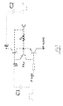
Fig. 11 shows a possible implementation of a Dickson charge pump circuit DCPC which can be used in the high side switch HS-SW as illustrated inFig. 10 . In the shown embodiment, the Dickson charge pump circuit DCPC comprises two pumping stages and an output stage. Each pumping stage comprises a charge transfer switch implemented by a high voltage depletion transistor as illustrated inFig. 11 . The bulk B of each high voltage depletion NMOS transistor is connected to a floating supply voltage V-low-sup whose potential is lower than an input voltage applied to the input of the respective pumping stage. In each pumping stage, a PMOS transistor P1 is connected between a source terminal S and the gate terminal G of the high voltage depletion NMOS transistor. Further, an NMOS transistor N1 is connected between the floating supply voltage and the gate terminal G of the high voltage depletion NMOS transistor of the respective pumping stage. The gate of the PMOS transistor P1 and the gate of the NMOS transistor N1 are connected to each other and receive a driving oscillation signal generated by the oscillation signal generation circuit OSGC. The first driving oscillation signal OSC1 is applied to the gates of the PMOS transistor P1 and the NMOS transistor N1 of the first pumping stage. The second driving oscillation signal OSC2 is applied to the capacitor C1 of the first pumping stage. A further driving oscillation signal OSC3 is applied to the gates of the PMOS transistor P2 and the NMOS transistor N2 of the second pumping stage as well as to the capacitor C2 of the second pumping stage. If the first oscillation signal OSC1 is logical high, the second driving oscillation signal OSC2 is also logical high but the third oscillation signal OSC3 is low. In a possible embodiment, the first oscillation signal OSC1 can be the same as the second driving oscillation signal OSC2. The output voltage V1 of the first pumping stage is applied as an input voltage to the second pumping stage. The output voltage V2 of the second pumping stage supplies is applied via an output switch to an output capacitor COUT having a higher capacitance than the capacitors C1 and C2 of the first and second pumping stage. Parallel to the output capacitor COUT a Zener Z diode can be provided. - The operation of a pumping stage within the Dickson charge pump circuit DCPC according to the present invention is further illustrated with respect to the pumping stage shown in
Fig. 12 and the corresponding signals illustrated inFig. 13 . As shown inFig. 12 , a charge transfer switch can be implemented by a high voltage depletion NMOS transistor whose gate G is connected to a junction node between a PMOS transistor P1 and an NMOS transistor N1. The PMOS transistor P1 is connected between the source terminal S and the gate terminal G of the high voltage depletion NMOS transistor of the pumping stage shown inFig. 12 . The NMOS transistor N1 is connected between the floating supply voltage applied at GND-CP and the gate terminal G of the high voltage depletion NMOS transistor of the pumping stage. The gate of the PMOS transistor P1 and the gate of the NMOS transistor N1 are connected to each other and receive a driving oscillation signal through a driving circuit as illustrated inFig. 12 . In the embodiment shown inFig. 12 , the driving oscillation signal applied to the gate terminals of the transistors P1, N1 is the same as the driving oscillation signal applied to the capacitor C of the respective pumping stage.Fig. 13 shows as a first signal diagram the current I1 flowing through the charge transfer switch implemented by the high voltage depletion NMOS transistor. The current I2 shown as a second diagram ofFig. 13 is the current flowing into the capacitor C of the pumping stage. The third signal diagram ofFig. 13 shows the current I3 flowing via the output of the pumping stage through an ideal switch to an output capacitor C0.Fig. 13 further shows the voltage VIN supplied to the input terminal IN of the pumping stage. Further, the voltage VC- at the negative terminal of the capacitor C is illustrated. The last signal diagram ofFig.13 shows the gate voltage VG at the gate terminal G of the high voltage depletion NMOS transistor forming the charge transfer switch.
Claims (11)
- A high side switch (HS-SW) comprising
a power switch (PS); and
a Dickson charge pump circuit (DCPC) configured to drive said power switch and having a pumping stage which has a charge transfer switch adapted to transfer an electrical charge from an input of the pumping stage to an output of the pumping stage,
wherein the charge transfer switch of the pumping stage comprises a depletion NMOS transistor (NMOS) having a bulk (B) connected to a supply voltage (VLOW-SUP) being lower than an input voltage applied to the input of the pumping stage, wherein the input of the pumping stage of said Dickson charge pump circuit (DCPC) is connected by means of a switchable supply voltage switch (SW-SUP) to a supply voltage (VS) provided by a battery, and
the input of the pumping stage of the Dickson charge pump circuit (DCPC) is connected by means of a Zener diode (Z) to the output of the power switch (PS) of said high side switch (HS-SW). - The high side switch (HS-SW) according to claim 1, wherein the pumping stage of said Dickson charge pump circuit (DCPC) comprises a charge transfer capacitor connected to the output of the pumping stage.
- The high side switch (HS-SW) according to claim 1 or 2, wherein driving oscillation signals generated by an oscillation signal generation circuit (OSGC) are applied to the charge transfer capacitor.
- The high side switch (HS-SW) according to one of the preceding claims 1 to 3, wherein a PMOS transistor (P1) is connected between a source terminal (S) and the gate terminal (G) of said depletion NMOS transistor of the pumping stage.
- The high side switch (HS-SW) according to claim 4, wherein a NMOS transistor (N1) is connected between the supply voltage and the gate terminal (G) of said depletion NMOS transistor of the pumping stage.
- The high side switch (HS-SW) according to claim 5, wherein the gate (G) of the PMOS transistor (P1) and the NMOS transistor (N1) are connected to each other and receive a further driving oscillation signal generated by the oscillation signal generation circuit (OSGC).
- The high side switch (HS-SW) according to one of the preceding claims 1 to 6, wherein the supply voltage is connected to the input voltage applied to the input of the pumping stage of the Dickson charge pump circuit (DCPC).
- The high side switch (HS-SW) according to one of the preceding claims 1 to 7, wherein said power switch (PS) of said high side switch (HS-SW) is a DMOS transistor driving a load (L).
- The high side switch (HS-SW) according to one of the preceding claims 1 to 8, wherein the supply voltage switch (SW-SUP) adapted to switch said Dickson charge pump circuit (DCPC) to said supply voltage (VS) is a MOS transistor having a gate connected to a signal input of said high side switch (HS-SW) which comprises said Dickson charge pump circuit (DCPC).
- The high side switch (HS-SW) according to one of the preceding claims 1 to 9, wherein said signal input of said high side switch (HS-SW) is connected to the gate of said supply voltage switch (SW-SUP) and a charging/discharging switch (SW D/C) being switchable between a charging current source (CCS) and a discharging current source (DCS) of said power switch (PS).
- The high side switch (HS-SW) according to one of the preceding claims 1 to 10, wherein the voltage drop (VD) of the switched on depletion NMOS transistor is less than 0.7 volts.
Priority Applications (1)
| Application Number | Priority Date | Filing Date | Title |
|---|---|---|---|
| EP13158227.2A EP2775621B1 (en) | 2013-03-07 | 2013-03-07 | A Dickson charge pump circuit |
Applications Claiming Priority (1)
| Application Number | Priority Date | Filing Date | Title |
|---|---|---|---|
| EP13158227.2A EP2775621B1 (en) | 2013-03-07 | 2013-03-07 | A Dickson charge pump circuit |
Publications (2)
| Publication Number | Publication Date |
|---|---|
| EP2775621A1 EP2775621A1 (en) | 2014-09-10 |
| EP2775621B1 true EP2775621B1 (en) | 2018-08-15 |
Family
ID=47832989
Family Applications (1)
| Application Number | Title | Priority Date | Filing Date |
|---|---|---|---|
| EP13158227.2A Active EP2775621B1 (en) | 2013-03-07 | 2013-03-07 | A Dickson charge pump circuit |
Country Status (1)
| Country | Link |
|---|---|
| EP (1) | EP2775621B1 (en) |
Families Citing this family (2)
| Publication number | Priority date | Publication date | Assignee | Title |
|---|---|---|---|---|
| PL3337002T3 (en) * | 2016-12-16 | 2023-10-09 | Samsung Sdi Co., Ltd | Battery system and control unit for a battery system |
| CN109946954B (en) * | 2019-04-01 | 2022-03-11 | 科华恒盛股份有限公司 | Voltage buffer circuit, device and control method thereof |
Family Cites Families (2)
| Publication number | Priority date | Publication date | Assignee | Title |
|---|---|---|---|---|
| US7592857B2 (en) * | 2007-12-21 | 2009-09-22 | G-Time Electronic Co., Ltd. | Charge pump circuit |
| US9112494B2 (en) * | 2011-07-28 | 2015-08-18 | Infineon Technologies Ag | Charge pump driven electronic switch with rapid turn off |
-
2013
- 2013-03-07 EP EP13158227.2A patent/EP2775621B1/en active Active
Non-Patent Citations (1)
| Title |
|---|
| None * |
Also Published As
| Publication number | Publication date |
|---|---|
| EP2775621A1 (en) | 2014-09-10 |
Similar Documents
| Publication | Publication Date | Title |
|---|---|---|
| KR101062265B1 (en) | Step-down switching regulator | |
| US9356514B2 (en) | Power supply conversion apparatus with bootstrap unit | |
| CN104796171B (en) | A kind of control circuit applied to SOI CMOS RF switches | |
| KR101316327B1 (en) | Driving circuit, semiconductor device having driving circuit, and switching regulator and electronic equipment using driving circuit and semiconductor device | |
| US9417642B2 (en) | Bootstrap DC-DC converter | |
| CN107888179B (en) | Semiconductor device | |
| CN203151371U (en) | Negative charge pump circuit | |
| US7388422B2 (en) | Charge pump circuit for high side drive circuit and driver driving voltage circuit | |
| EP2337200B1 (en) | A sub-stage for a charge pump | |
| CN102769379A (en) | Positive and negative voltage generation circuit applicable to silicon-on-insulator (SOI) process | |
| JP6031883B2 (en) | Semiconductor integrated circuit and power supply circuit | |
| KR102279558B1 (en) | Elementary cell and charge pumps comprising such an elementary cell | |
| CN110199238A (en) | Output circuit and for provide output electric current method | |
| US9774250B2 (en) | Cold start DC/DC converter | |
| US20130294123A1 (en) | Charge pump | |
| EP2775621A1 (en) | A Dickson charge pump circuit | |
| CN107968563B (en) | Charge pump | |
| US20090309650A1 (en) | Booster circuit | |
| CN107453602B (en) | Charge pump and memory device | |
| US8253477B2 (en) | Voltage boost circuit without device overstress | |
| US9431901B2 (en) | Charge pump stage and a charge pump | |
| KR100925326B1 (en) | DC-DC converter | |
| CN116169863A (en) | A device for realizing accelerated drive of NMOS tube | |
| US7772919B2 (en) | Double stage compact charge pump circuit | |
| EP4701029A1 (en) | Charging circuit for a capacitive component, power circuit and vehicle |
Legal Events
| Date | Code | Title | Description |
|---|---|---|---|
| PUAI | Public reference made under article 153(3) epc to a published international application that has entered the european phase |
Free format text: ORIGINAL CODE: 0009012 |
|
| 17P | Request for examination filed |
Effective date: 20130307 |
|
| AK | Designated contracting states |
Kind code of ref document: A1 Designated state(s): AL AT BE BG CH CY CZ DE DK EE ES FI FR GB GR HR HU IE IS IT LI LT LU LV MC MK MT NL NO PL PT RO RS SE SI SK SM TR |
|
| AX | Request for extension of the european patent |
Extension state: BA ME |
|
| R17P | Request for examination filed (corrected) |
Effective date: 20150310 |
|
| RBV | Designated contracting states (corrected) |
Designated state(s): AL AT BE BG CH CY CZ DE DK EE ES FI FR GB GR HR HU IE IS IT LI LT LU LV MC MK MT NL NO PL PT RO RS SE SI SK SM TR |
|
| 17Q | First examination report despatched |
Effective date: 20151223 |
|
| GRAP | Despatch of communication of intention to grant a patent |
Free format text: ORIGINAL CODE: EPIDOSNIGR1 |
|
| STAA | Information on the status of an ep patent application or granted ep patent |
Free format text: STATUS: GRANT OF PATENT IS INTENDED |
|
| INTG | Intention to grant announced |
Effective date: 20180130 |
|
| GRAS | Grant fee paid |
Free format text: ORIGINAL CODE: EPIDOSNIGR3 |
|
| GRAA | (expected) grant |
Free format text: ORIGINAL CODE: 0009210 |
|
| STAA | Information on the status of an ep patent application or granted ep patent |
Free format text: STATUS: THE PATENT HAS BEEN GRANTED |
|
| AK | Designated contracting states |
Kind code of ref document: B1 Designated state(s): AL AT BE BG CH CY CZ DE DK EE ES FI FR GB GR HR HU IE IS IT LI LT LU LV MC MK MT NL NO PL PT RO RS SE SI SK SM TR |
|
| REG | Reference to a national code |
Ref country code: CH Ref legal event code: EP Ref country code: GB Ref legal event code: FG4D Ref country code: AT Ref legal event code: REF Ref document number: 1030940 Country of ref document: AT Kind code of ref document: T Effective date: 20180815 |
|
| REG | Reference to a national code |
Ref country code: IE Ref legal event code: FG4D |
|
| REG | Reference to a national code |
Ref country code: DE Ref legal event code: R096 Ref document number: 602013041911 Country of ref document: DE |
|
| REG | Reference to a national code |
Ref country code: NL Ref legal event code: MP Effective date: 20180815 |
|
| REG | Reference to a national code |
Ref country code: LT Ref legal event code: MG4D |
|
| REG | Reference to a national code |
Ref country code: AT Ref legal event code: MK05 Ref document number: 1030940 Country of ref document: AT Kind code of ref document: T Effective date: 20180815 |
|
| PG25 | Lapsed in a contracting state [announced via postgrant information from national office to epo] |
Ref country code: NO Free format text: LAPSE BECAUSE OF FAILURE TO SUBMIT A TRANSLATION OF THE DESCRIPTION OR TO PAY THE FEE WITHIN THE PRESCRIBED TIME-LIMIT Effective date: 20181115 Ref country code: BG Free format text: LAPSE BECAUSE OF FAILURE TO SUBMIT A TRANSLATION OF THE DESCRIPTION OR TO PAY THE FEE WITHIN THE PRESCRIBED TIME-LIMIT Effective date: 20181115 Ref country code: GR Free format text: LAPSE BECAUSE OF FAILURE TO SUBMIT A TRANSLATION OF THE DESCRIPTION OR TO PAY THE FEE WITHIN THE PRESCRIBED TIME-LIMIT Effective date: 20181116 Ref country code: SE Free format text: LAPSE BECAUSE OF FAILURE TO SUBMIT A TRANSLATION OF THE DESCRIPTION OR TO PAY THE FEE WITHIN THE PRESCRIBED TIME-LIMIT Effective date: 20180815 Ref country code: FI Free format text: LAPSE BECAUSE OF FAILURE TO SUBMIT A TRANSLATION OF THE DESCRIPTION OR TO PAY THE FEE WITHIN THE PRESCRIBED TIME-LIMIT Effective date: 20180815 Ref country code: LT Free format text: LAPSE BECAUSE OF FAILURE TO SUBMIT A TRANSLATION OF THE DESCRIPTION OR TO PAY THE FEE WITHIN THE PRESCRIBED TIME-LIMIT Effective date: 20180815 Ref country code: RS Free format text: LAPSE BECAUSE OF FAILURE TO SUBMIT A TRANSLATION OF THE DESCRIPTION OR TO PAY THE FEE WITHIN THE PRESCRIBED TIME-LIMIT Effective date: 20180815 Ref country code: NL Free format text: LAPSE BECAUSE OF FAILURE TO SUBMIT A TRANSLATION OF THE DESCRIPTION OR TO PAY THE FEE WITHIN THE PRESCRIBED TIME-LIMIT Effective date: 20180815 Ref country code: IS Free format text: LAPSE BECAUSE OF FAILURE TO SUBMIT A TRANSLATION OF THE DESCRIPTION OR TO PAY THE FEE WITHIN THE PRESCRIBED TIME-LIMIT Effective date: 20181215 Ref country code: AT Free format text: LAPSE BECAUSE OF FAILURE TO SUBMIT A TRANSLATION OF THE DESCRIPTION OR TO PAY THE FEE WITHIN THE PRESCRIBED TIME-LIMIT Effective date: 20180815 |
|
| PG25 | Lapsed in a contracting state [announced via postgrant information from national office to epo] |
Ref country code: LV Free format text: LAPSE BECAUSE OF FAILURE TO SUBMIT A TRANSLATION OF THE DESCRIPTION OR TO PAY THE FEE WITHIN THE PRESCRIBED TIME-LIMIT Effective date: 20180815 Ref country code: AL Free format text: LAPSE BECAUSE OF FAILURE TO SUBMIT A TRANSLATION OF THE DESCRIPTION OR TO PAY THE FEE WITHIN THE PRESCRIBED TIME-LIMIT Effective date: 20180815 Ref country code: HR Free format text: LAPSE BECAUSE OF FAILURE TO SUBMIT A TRANSLATION OF THE DESCRIPTION OR TO PAY THE FEE WITHIN THE PRESCRIBED TIME-LIMIT Effective date: 20180815 |
|
| PG25 | Lapsed in a contracting state [announced via postgrant information from national office to epo] |
Ref country code: EE Free format text: LAPSE BECAUSE OF FAILURE TO SUBMIT A TRANSLATION OF THE DESCRIPTION OR TO PAY THE FEE WITHIN THE PRESCRIBED TIME-LIMIT Effective date: 20180815 Ref country code: PL Free format text: LAPSE BECAUSE OF FAILURE TO SUBMIT A TRANSLATION OF THE DESCRIPTION OR TO PAY THE FEE WITHIN THE PRESCRIBED TIME-LIMIT Effective date: 20180815 Ref country code: IT Free format text: LAPSE BECAUSE OF FAILURE TO SUBMIT A TRANSLATION OF THE DESCRIPTION OR TO PAY THE FEE WITHIN THE PRESCRIBED TIME-LIMIT Effective date: 20180815 Ref country code: RO Free format text: LAPSE BECAUSE OF FAILURE TO SUBMIT A TRANSLATION OF THE DESCRIPTION OR TO PAY THE FEE WITHIN THE PRESCRIBED TIME-LIMIT Effective date: 20180815 Ref country code: CZ Free format text: LAPSE BECAUSE OF FAILURE TO SUBMIT A TRANSLATION OF THE DESCRIPTION OR TO PAY THE FEE WITHIN THE PRESCRIBED TIME-LIMIT Effective date: 20180815 Ref country code: ES Free format text: LAPSE BECAUSE OF FAILURE TO SUBMIT A TRANSLATION OF THE DESCRIPTION OR TO PAY THE FEE WITHIN THE PRESCRIBED TIME-LIMIT Effective date: 20180815 |
|
| REG | Reference to a national code |
Ref country code: DE Ref legal event code: R097 Ref document number: 602013041911 Country of ref document: DE |
|
| PG25 | Lapsed in a contracting state [announced via postgrant information from national office to epo] |
Ref country code: SK Free format text: LAPSE BECAUSE OF FAILURE TO SUBMIT A TRANSLATION OF THE DESCRIPTION OR TO PAY THE FEE WITHIN THE PRESCRIBED TIME-LIMIT Effective date: 20180815 Ref country code: DK Free format text: LAPSE BECAUSE OF FAILURE TO SUBMIT A TRANSLATION OF THE DESCRIPTION OR TO PAY THE FEE WITHIN THE PRESCRIBED TIME-LIMIT Effective date: 20180815 Ref country code: SM Free format text: LAPSE BECAUSE OF FAILURE TO SUBMIT A TRANSLATION OF THE DESCRIPTION OR TO PAY THE FEE WITHIN THE PRESCRIBED TIME-LIMIT Effective date: 20180815 |
|
| PLBE | No opposition filed within time limit |
Free format text: ORIGINAL CODE: 0009261 |
|
| STAA | Information on the status of an ep patent application or granted ep patent |
Free format text: STATUS: NO OPPOSITION FILED WITHIN TIME LIMIT |
|
| 26N | No opposition filed |
Effective date: 20190516 |
|
| PG25 | Lapsed in a contracting state [announced via postgrant information from national office to epo] |
Ref country code: SI Free format text: LAPSE BECAUSE OF FAILURE TO SUBMIT A TRANSLATION OF THE DESCRIPTION OR TO PAY THE FEE WITHIN THE PRESCRIBED TIME-LIMIT Effective date: 20180815 |
|
| PG25 | Lapsed in a contracting state [announced via postgrant information from national office to epo] |
Ref country code: MC Free format text: LAPSE BECAUSE OF FAILURE TO SUBMIT A TRANSLATION OF THE DESCRIPTION OR TO PAY THE FEE WITHIN THE PRESCRIBED TIME-LIMIT Effective date: 20180815 |
|
| REG | Reference to a national code |
Ref country code: CH Ref legal event code: PL |
|
| GBPC | Gb: european patent ceased through non-payment of renewal fee |
Effective date: 20190307 |
|
| PG25 | Lapsed in a contracting state [announced via postgrant information from national office to epo] |
Ref country code: LU Free format text: LAPSE BECAUSE OF NON-PAYMENT OF DUE FEES Effective date: 20190307 |
|
| REG | Reference to a national code |
Ref country code: BE Ref legal event code: MM Effective date: 20190331 |
|
| PG25 | Lapsed in a contracting state [announced via postgrant information from national office to epo] |
Ref country code: IE Free format text: LAPSE BECAUSE OF NON-PAYMENT OF DUE FEES Effective date: 20190307 Ref country code: LI Free format text: LAPSE BECAUSE OF NON-PAYMENT OF DUE FEES Effective date: 20190331 Ref country code: CH Free format text: LAPSE BECAUSE OF NON-PAYMENT OF DUE FEES Effective date: 20190331 Ref country code: GB Free format text: LAPSE BECAUSE OF NON-PAYMENT OF DUE FEES Effective date: 20190307 |
|
| PG25 | Lapsed in a contracting state [announced via postgrant information from national office to epo] |
Ref country code: BE Free format text: LAPSE BECAUSE OF NON-PAYMENT OF DUE FEES Effective date: 20190331 Ref country code: FR Free format text: LAPSE BECAUSE OF NON-PAYMENT OF DUE FEES Effective date: 20190331 |
|
| PG25 | Lapsed in a contracting state [announced via postgrant information from national office to epo] |
Ref country code: TR Free format text: LAPSE BECAUSE OF FAILURE TO SUBMIT A TRANSLATION OF THE DESCRIPTION OR TO PAY THE FEE WITHIN THE PRESCRIBED TIME-LIMIT Effective date: 20180815 |
|
| PG25 | Lapsed in a contracting state [announced via postgrant information from national office to epo] |
Ref country code: PT Free format text: LAPSE BECAUSE OF FAILURE TO SUBMIT A TRANSLATION OF THE DESCRIPTION OR TO PAY THE FEE WITHIN THE PRESCRIBED TIME-LIMIT Effective date: 20181215 Ref country code: MT Free format text: LAPSE BECAUSE OF NON-PAYMENT OF DUE FEES Effective date: 20190307 |
|
| PG25 | Lapsed in a contracting state [announced via postgrant information from national office to epo] |
Ref country code: CY Free format text: LAPSE BECAUSE OF FAILURE TO SUBMIT A TRANSLATION OF THE DESCRIPTION OR TO PAY THE FEE WITHIN THE PRESCRIBED TIME-LIMIT Effective date: 20180815 |
|
| PG25 | Lapsed in a contracting state [announced via postgrant information from national office to epo] |
Ref country code: HU Free format text: LAPSE BECAUSE OF FAILURE TO SUBMIT A TRANSLATION OF THE DESCRIPTION OR TO PAY THE FEE WITHIN THE PRESCRIBED TIME-LIMIT; INVALID AB INITIO Effective date: 20130307 |
|
| PG25 | Lapsed in a contracting state [announced via postgrant information from national office to epo] |
Ref country code: MK Free format text: LAPSE BECAUSE OF FAILURE TO SUBMIT A TRANSLATION OF THE DESCRIPTION OR TO PAY THE FEE WITHIN THE PRESCRIBED TIME-LIMIT Effective date: 20180815 |
|
| P01 | Opt-out of the competence of the unified patent court (upc) registered |
Effective date: 20230512 |
|
| PGFP | Annual fee paid to national office [announced via postgrant information from national office to epo] |
Ref country code: DE Payment date: 20260128 Year of fee payment: 14 |