EP2775571A1 - Sense pin for an electrical connector - Google Patents
Sense pin for an electrical connector Download PDFInfo
- Publication number
- EP2775571A1 EP2775571A1 EP14156945.9A EP14156945A EP2775571A1 EP 2775571 A1 EP2775571 A1 EP 2775571A1 EP 14156945 A EP14156945 A EP 14156945A EP 2775571 A1 EP2775571 A1 EP 2775571A1
- Authority
- EP
- European Patent Office
- Prior art keywords
- electrical
- mating
- segment
- sense pin
- tip
- Prior art date
- Legal status (The legal status is an assumption and is not a legal conclusion. Google has not performed a legal analysis and makes no representation as to the accuracy of the status listed.)
- Granted
Links
Images



Classifications
-
- H—ELECTRICITY
- H01—ELECTRIC ELEMENTS
- H01R—ELECTRICALLY-CONDUCTIVE CONNECTIONS; STRUCTURAL ASSOCIATIONS OF A PLURALITY OF MUTUALLY-INSULATED ELECTRICAL CONNECTING ELEMENTS; COUPLING DEVICES; CURRENT COLLECTORS
- H01R13/00—Details of coupling devices of the kinds covered by groups H01R12/70 or H01R24/00 - H01R33/00
- H01R13/66—Structural association with built-in electrical component
- H01R13/665—Structural association with built-in electrical component with built-in electronic circuit
- H01R13/6683—Structural association with built-in electrical component with built-in electronic circuit with built-in sensor
-
- H—ELECTRICITY
- H01—ELECTRIC ELEMENTS
- H01R—ELECTRICALLY-CONDUCTIVE CONNECTIONS; STRUCTURAL ASSOCIATIONS OF A PLURALITY OF MUTUALLY-INSULATED ELECTRICAL CONNECTING ELEMENTS; COUPLING DEVICES; CURRENT COLLECTORS
- H01R13/00—Details of coupling devices of the kinds covered by groups H01R12/70 or H01R24/00 - H01R33/00
- H01R13/40—Securing contact members in or to a base or case; Insulating of contact members
- H01R13/405—Securing in non-demountable manner, e.g. moulding, riveting
-
- H—ELECTRICITY
- H01—ELECTRIC ELEMENTS
- H01R—ELECTRICALLY-CONDUCTIVE CONNECTIONS; STRUCTURAL ASSOCIATIONS OF A PLURALITY OF MUTUALLY-INSULATED ELECTRICAL CONNECTING ELEMENTS; COUPLING DEVICES; CURRENT COLLECTORS
- H01R13/00—Details of coupling devices of the kinds covered by groups H01R12/70 or H01R24/00 - H01R33/00
- H01R13/64—Means for preventing incorrect coupling
- H01R13/641—Means for preventing incorrect coupling by indicating incorrect coupling; by indicating correct or full engagement
-
- H—ELECTRICITY
- H01—ELECTRIC ELEMENTS
- H01R—ELECTRICALLY-CONDUCTIVE CONNECTIONS; STRUCTURAL ASSOCIATIONS OF A PLURALITY OF MUTUALLY-INSULATED ELECTRICAL CONNECTING ELEMENTS; COUPLING DEVICES; CURRENT COLLECTORS
- H01R43/00—Apparatus or processes specially adapted for manufacturing, assembling, maintaining, or repairing of line connectors or current collectors or for joining electric conductors
- H01R43/20—Apparatus or processes specially adapted for manufacturing, assembling, maintaining, or repairing of line connectors or current collectors or for joining electric conductors for assembling or disassembling contact members with insulating base, case or sleeve
- H01R43/24—Assembling by moulding on contact members
-
- H—ELECTRICITY
- H01—ELECTRIC ELEMENTS
- H01R—ELECTRICALLY-CONDUCTIVE CONNECTIONS; STRUCTURAL ASSOCIATIONS OF A PLURALITY OF MUTUALLY-INSULATED ELECTRICAL CONNECTING ELEMENTS; COUPLING DEVICES; CURRENT COLLECTORS
- H01R13/00—Details of coupling devices of the kinds covered by groups H01R12/70 or H01R24/00 - H01R33/00
- H01R13/66—Structural association with built-in electrical component
- H01R13/70—Structural association with built-in electrical component with built-in switch
- H01R13/703—Structural association with built-in electrical component with built-in switch operated by engagement or disengagement of coupling parts, e.g. dual-continuity coupling part
- H01R13/7031—Shorting, shunting or bussing of different terminals interrupted or effected on engagement of coupling part, e.g. for ESD protection, line continuity
- H01R13/7034—Shorting, shunting or bussing of different terminals interrupted or effected on engagement of coupling part, e.g. for ESD protection, line continuity the terminals being in direct electric contact separated by double sided connecting element
-
- H—ELECTRICITY
- H01—ELECTRIC ELEMENTS
- H01R—ELECTRICALLY-CONDUCTIVE CONNECTIONS; STRUCTURAL ASSOCIATIONS OF A PLURALITY OF MUTUALLY-INSULATED ELECTRICAL CONNECTING ELEMENTS; COUPLING DEVICES; CURRENT COLLECTORS
- H01R2107/00—Four or more poles
Definitions
- the invention relates to an electrical connector having a sense pin.
- the electrical contacts of the electrical connectors may remain engaged in physical and electrical contact before the electrical connectors are fully de-mated from each other.
- the electrical performance of the assembly will degrade when the electrical connectors are de-mated beyond a de-mating distance that is less than the fully de-mated distance. For example, the amount of electrical power and/or the speed, strength, and/or number of electrical signals transmitted through the assembly may be reduced.
- Some electrical connector assemblies include sense pins for indicating whether the electrical contacts of a mated pair of electrical connectors have achieved a predetermined wipe length that provides a reliable electrical connection between corresponding electrical contacts.
- Such known sense pins could be used to detect whether the mated pair of electrical connectors have been de-mated beyond a distance at which the electrical performance of the assembly begins to degrade. But, the detection range of known sense pins is too broad.
- the tips of known sense pins include guide features such as chamfers, fillets, and/or rounds that guide initial engagement between the sense pin and the corresponding electrical contact of the other electrical connector.
- the unreliable segment of the wipe length may cause the sense pin to falsely indicate that the electrical contacts are still within a predetermined de-mating distance beyond which electrical performance degrades. Such a false indication may cause the electrical connector assembly to be unknowingly operated with degraded electrical performance.
- the unreliable segment of the wipe length may also cause the sense pin to falsely indicate that the electrical contacts are de-mated beyond the predetermined de-mating distance, which may cause the unnecessary diversion of the functionality of the electrical connector assembly to other resources.
- an electrical connector comprises a housing and electrical contacts held by the housing.
- the electrical contacts are configured to mate with corresponding mating contacts of a mating connector.
- the housing holds a sense pin that is configured to mate with a corresponding mating contact of the mating connector.
- the sense pin extends a length that includes a tip segment and a sensing segment having respective different electrical characteristics.
- the tip segment extends from the sensing segment to a tip of the sense pin such that the sensing segment is offset from the tip along the length of the sense pin.
- the sensing segment is configured to indicate that the electrical contacts and the mating contacts are de-mated by more than a predetermined de-mating distance.
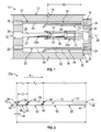
- FIG 1 is a cross-sectional view of an exemplary embodiment of an electrical connector assembly 10.
- the electrical connector assembly 10 includes electrical connectors 12 and 14 that are configured to mate together along a connection axis 16.
- the electrical connectors 12 and 14 include respective housings 18 and 20 and respective electrical contacts 22 and 24.
- the electrical contacts 22 of the electrical connector 12 are mated with corresponding electrical contacts 24 of the electrical connector 14, thereby establishing an electrical connection between the electrical connectors 12 and 14.
- one or more of the electrical contacts 22 of the electrical connector 12 is a sense pin 22a that is configured to indicate when the electrical connectors 12 and 14 are de-mated by more than a predetermined de-mating distance PDD ( Figure 3 ).
- the electrical contacts 22 of the electrical connector 12 are held by the housing 18 of the electrical connector 12.
- the electrical contacts 22 include bases 26 and mating segments 28 that extend from the bases 26.
- the bases 26 are held by the housing 18 and the housing 18 is configured such that the mating segments 28 extend within corresponding mating receptacles 30 of the housing 18.
- one or more of the mating segments 28 extends outward from a mating end 32 of the housing 18, whether or not the mating segment(s) 28 is configured to be received within a corresponding mating receptacle (not shown) of the electrical connector 14.
- the electrical contacts 24 of the electrical connector 14 include bases 34 and mating segments 36 that extend from the bases 34.
- the bases 34 of the electrical contacts 24 are held by the housing 20 and the housing 20 is configured such that the mating segments 36 extend outward from a mating end 38 of the housing 20 for being received within one or more corresponding mating receptacles 30 of the electrical connector 12.
- one or more of the mating segments 36 extends outward from the mating end 38 but is not configured to be received within a corresponding mating receptacle 30 of the electrical connector 12.
- the mating segment 36 of one or more electrical contacts 24 extends within a corresponding mating receptacle (not shown) of the housing 20 for mating with the corresponding electrical contact 22 within the mating receptacle.
- the electrical contacts 24 of the electrical connector 14 may be referred to herein as "mating contacts”.
- the electrical connector 14 may be referred to herein as a "mating connector”.
- the electrical connectors 12 and 14 are shown in Figure 1 in a fully mated position.
- the housings 18 and 20 are brought towards each other along the connection axis 16.
- the electrical contacts 22 of the electrical connector 12 mate with the electrical contacts 24 of the electrical connector 14.
- the mating segments 28 of the electrical contacts 22 move into physical contact with the mating segments 36 of the corresponding electrical contacts 24 of the electrical connector 14.
- the mating segments 28 slide along the corresponding mating segments 36, in physical contact therewith, until the mating segments 28 and 36 are in the fully mated positions shown in Figure 1 .
- the physical contact between the mating segments 28 and 36 establishes an electrical connection between the mating segments 38 and 36, and thus between the corresponding electrical contacts 22 and 24.
- “mated” it is meant that corresponding mating segments 28 and 36 are engaged in physical contact such that an electrical connection is established having a predetermined reliability, strength, and/or the like.
- the electrical contacts 24 of the electrical connector 14 mate with the electrical contacts 22 of the electrical connector 12 within the corresponding mating receptacles 30 of the electrical connector 12.
- the electrical contacts 22 and 24 slide along each other along a wipe length WL.
- the wipe length WL is defined by the distance along which the mating segments 28 and 36 slide in physical contact with each other.
- the dimension of the wipe length WL of the electrical contacts 22 and 24 may be selected as a distance that establishes an electrical connection between the corresponding mating segments 28 and 36 that has a predetermined reliability, strength, and/or the like.
- the dimension of the wipe length WL may be selected such that the sliding physical contact between mating segments 28 and 36 wipes through oxidation and/or other surface layers of the mating segments 28 and 36 at one or more points of physical contact between the mating segments 28 and 36.
- the mating ends 32 and 38 of the housings 18 and 20, respectively may not abut when the electrical connectors 12 and 14 are in the fully mated position.
- the mating end 32 of the housing 18 is received into a receptacle (not shown) of the mating end 38 of the housing 20, or vice versa, when the electrical connectors 12 and 14 are in the fully mated position.
- Each of the electrical connectors 12 and 14 may include any number of the respective electrical contacts 22 and 24.
- the electrical connector 12 may include any number of the mating receptacles 30, each of which may hold any number of mating segments 28 and may receive any number of mating segments 36 therein.
- Each electrical contact 22 and each electrical contact 24 may be any type of electrical contact, such as, but not limited to, a signal contact, a ground contact, an electrical power contact, a sense contact, and/or the like.
- one or more of the electrical contacts 22 of the electrical connector 12 is a sense pin 22a that is configured to indicate when the electrical connectors 12 and 14 are de-mated by more than a predetermined de-mating distance PDD.
- the sense pin 22a is configured to mate with a corresponding electrical contact 24a of the electrical connector 14.
- Figure 2 is an elevational view of an exemplary embodiment of a portion of the sense pin 22a.
- the base 26 ( Figure 1 ) of the sense pin 22a is not shown in Figure 2 . Rather, only the mating segment 28 of the sense pin 22a is shown in Figure 2 for clarity.
- the mating segment 28 of the sense pin 22a extends a length L along a central longitudinal axis 40 from an end 42 of the mating segment 28 to a tip 44 of the sense pin 22a.
- the tip 44 includes a tip surface 46.
- the tip 44 optionally includes one or more guide features such as, but not limited to, a chamfer, a round, a fillet, and/or the like.
- the tip 44 includes a chamfer 48.
- the length L of the mating segment 28 of the sense pin 22a includes a base segment 50, an intermediate segment 52, and a tip segment 54.
- the base segment 50 extends a length L 1 from the base 26 of the sense pin 22a to an end 56 of the base segment 50.
- the base segment 50 includes the end 42 of the mating segment 28 of the sense pin 22a.
- the end 42 defines an end of the base segment 50 that is opposite the end 56.
- the intermediate segment 52 extends a length L 2 from an end 58 to an opposite end 60.
- the end 58 of the intermediate segment 52 extends from the end 56 of the base segment 50.
- the length L 2 of the intermediate segment 52 extends from the end 56 of the base segment 50 to the tip segment 54.
- the intermediate segment 52 extends between the base segment 50 and the tip segment 54 along the length L of the mating segment 28 of the sense pin 22a.
- the tip segment 54 includes the tip 44 of the sense pin 22a.
- the tip segment 54 extends a length L 3 from an end 62 to the tip 44, and more specifically from the end 62 to the tip surface 46.
- the end 62 of the tip segment 54 extends from the end 60 of the intermediate segment 52.
- the tip segment 54 extends between the intermediate segment 52 and the tip 44 along the length L of the mating segment 28 of the sense pin 22a. Accordingly, the intermediate segment 52 is displaced by an offset O from the tip 44 along the length L of the mating segment 28 of the sense pin 22a in the direction of the arrow A.
- the intermediate segment 52 is displaced by an offset O (in the direction A) from the chamfer 48 along the length L of the mating segment 28 of the sense pin 22a.
- the offset O may have any positive, non-zero, value.
- the tip 44 extends a length that extends from an end 64 of the chamfer 48 to the tip surface 46.
- the end 64 of the chamfer 48 defines an interior end of the tip 44.
- the intermediate segment 52 is offset from both the chamfer 48 and the tip 44 by the same offset O (i.e., by the same distance).
- the intermediate segment 52 will be offset (in the direction A) from the interior end of the tip 44 and from the end 64 of the chamfer 48 by different distances.
- the intermediate segment 52 may be offset (in the direction A) from the interior end of the tip 44 by any positive, non-zero, distance and may be offset (in the direction A) from the end 64 of the chamfer 48 by any positive, non-zero, distance.
- the intermediate segment 52 will be offset from the other guide feature in a substantially similar manner to the offsets from the chamfer 48 described and/or illustrated herein (e.g., the offset O).
- the intermediate segment 52 and the tip segment 54 include respective surface materials 66 and 68.
- the surface materials 66 and 68 have different electrical characteristics such that the intermediate segment 52 and the tip segment 54 have different electrical characteristics.
- one of the segments 52 or 54 is electrically conductive at the surface thereof, while the other segment 52 or 54 is electrically non-conductive at the surface thereof.
- the surface material 66 of the intermediate segment 52 is electrically non-conductive such that the intermediate segment 52 is electrically non-conductive
- the surface material 68 of the tip segment 54 is electrically conductive such that the tip segment 54 is electrically conductive.
- the surface materials 66 may be formed in any manner.
- the mating segment 28 of the sense pin 22a is defined by a body 70 that is electrically conductive and the surface material 66 of the intermediate segment 52 is defined by an electrically non-conductive coating that is formed on the body 70.
- the electrically conductive surface material 68 of the tip segment 54 may be defined by a surface of the body 70 or may be defined by an electrically conductive coating that is formed on the body 70.
- the body 70 is electrically non-conductive and the surface material 68 of the tip segment 54 is defined by an electrically conductive coating that is formed on the body 70.
- the electrically non-conductive surface material 66 of the intermediate segment 52 may be defined by a surface of the body 70 or may be defined by an electrically non-conductive coating that is formed on the body 70.
- the surface material 66, the surface material 68, and the body 70 may each be fabricated from any material(s) that provide the surface material 66, the surface material 68, and the body 70 with the electrical characteristics described and/or illustrated herein.
- the sense pin 22a is configured to indicate when the electrical connectors 12 and 14 are de-mated by more than a predetermined de-mating distance PDD.
- the intermediate segment 52 of the sense pin 22a is in physical contact with the corresponding electrical contact 24a when the electrical connectors 12 and 14 are fully mated together.
- the intermediate segment 52 is in physical contact with the electrical contact 24a at one or more contact regions 74 of the electrical contact 24a when the electrical connectors 12 and 14 are fully mated together.
- the connectors 12 and 14 are moved apart from one another along the connection axis 16.
- Figure 3 is a cross-sectional view of the electrical connector assembly 10 illustrating the electrical connectors 12 and 14 as partially de-mated from each other. Specifically, the electrical connectors 12 and 14 are de-mated by slightly more than the predetermined de-mating distance PDD in Figure 3 .
- the predetermined de-mating distance PDD may be a distance beyond which the electrical performance of the electrical connector assembly 10 begins to degrade.
- the electrical contacts 22 of the electrical connector 12 remain electrically connected to the corresponding electrical contacts 24 of the electrical connector 14 until the electrical connectors 12 and 14 have moved away from each other by greater than the wipe length WL ( Figure 1 ).
- the electrical contacts 22 are disengaged from physical contact with the corresponding electrical contacts 24 such that there is no electrical connection between the electrical contacts 22 and 24. The electrical connectors 12 and 14 are thereby fully de-mated.
- electrical performance degradation of the electrical connector assembly 10 may include, but is not limited to, a reduction in the speed, quality, strength, amount, number, and/or the like of electrical signals transmitted through the assembly 10, a reduction in the speed, quality, strength, amount, and/or the like of electrical power transmitted through the assembly 10, and/or the like.
- the predetermined de-mating distance PDD is the de-mating distance beyond which the electrical performance of the electrical connector assembly 10 begins to degrade.
- the predetermined de-mating distance PDD is the upper limit of the de-mating distance before the performance of the electrical connector assembly 10 begins to degrade. It should be appreciated that because the electrical contacts 22 and 24 are still engaged in physical and electrical contact with each other at the predetermined de-mating distance PDD, the predetermined de-mating distance PDD is less than the wipe length WL of the electrical contacts 22 and 24.
- the contact regions 74 of the electrical contact 24a slide along, in physical contact with, the intermediate segment 52 of the sense pin 22a.
- the transition between the intermediate segment 52 and the tip segment 54 is positioned along the length L of the sense pin 22a at a position that corresponds to the predetermined de-mating distance PDD.
- the end 60 of the intermediate segment 52 is positioned along the length L ( Figure 2 ) of the mating segment 28 of the sense pin 22a such that the intermediate segment 52 is moved out of physical contact with (i.e., disengaged from) the contact regions 74 of the electrical contact 24a as the sense pin 22a and the electrical contact 24a are de-mated beyond the predetermined de-mating distance PDD.
- the end 62 of the tip segment 54 is positioned along the length L of the mating segment 28 of the sense pin 22a such that the tip segment 54 is moved into physical contact with the contact regions 74 of the electrical contact 24a as the sense pin 22a and the electrical contact 24a are de-mated beyond the predetermined de-mating distance PDD.
- the electrical connectors 12 and 14 are shown in Figure 3 as being de-mated by slightly more than the predetermined de-mating distance PDD. Specifically, the contact regions 74 of the electrical contact 24a are engaged in physical contact with the tip segment 54 of the sense pin 22a but are disengaged from the intermediate segment 52 of the sense pin 22a. In the exemplary embodiment of the electrical connector assembly 10, the physical contact between the contact regions 74 of the electrical contact 24a and the electrically conductive surface material 68 of the tip segment 54 closes an electrical connection between the sense pin 22a and the electrical contact 24a. The closing of the electrical connection indicates that the electrical contacts 22 of the electrical connector 12 are de-mated from the corresponding electrical contacts 24 of the electrical connector 14 by more than the predetermined de-mating distance PDD.
- the intermediate segment 52 is configured to indicate that the electrical contacts 22 and 24 are de-mated by more than the predetermined de-mating distance PDD by disengaging from physical contact with the contact regions 74 of the electrical contact 24a.
- the contact regions 74 disengage from physical contact with the intermediate segment 52 and engage in physical contact with the tip segment 54 to thereby close the electrical connection between the sense pin 22a and the electrical contact 24a.
- the base 26 ( Figure 1 ) of the sense pin 22a may be operatively connected to a processor, logic, controller, computer, circuit, and/or like for receiving and processing the indication (i.e., the closing of the electrical connection) from the sense pin 22a.
- the intermediate segment 52 of the sense pin 22a is configured to indicate that the electrical contacts 22 and 24 are de-mated by more than the predetermined de-mating distance PDD by disengaging from physical contact with the contact regions 74 of the electrical contact 24a, the intermediate segment 52 may be considered, and referred to herein, as a "sensing segment" of the sense pin 22a.
- FIG 4 is a cross-sectional view of another exemplary embodiment of an electrical connector assembly 110.
- the electrical connector assembly 110 includes electrical connectors 112 and 114 that are configured to mate together along a connection axis 116.
- the electrical connectors 112 and 114 include respective housings 118 and 120 and respective electrical contacts 122 and 124.
- One or more of the electrical contacts 122 of the electrical connector 112 is a sense pin 122a that is configured to indicate when the electrical connectors 112 and 114 are de-mated beyond a predetermined de-mating distance PDD 1 ( Figure 5 ).
- the electrical contacts 124 of the electrical connector 114 may be referred to herein as "mating contacts”.
- the electrical connector 114 may be referred to herein as a "mating connector”.
- the sense pin 122a includes a mating segment 128 that extends a length from an end 142 of the mating segment 128 to a tip 144 of the sense pin 122a.
- the tip 144 includes a tip surface 146.
- the tip 144 optionally includes one or more guide features, such as, but not limited to, a chamfer, a round, a fillet, and/or the like.
- the tip 144 includes a chamfer 148.
- the length of the mating segment 128 of the sense pin 122a includes a base segment 150, an intermediate segment 152, and a tip segment 154.
- the intermediate segment 152 extends a length from an end 158 to an opposite end 160.
- the intermediate segment 152 extends between the base segment 150 and the tip segment 154 along the length of the mating segment 128 of the sense pin 122a.
- the tip segment 154 includes the tip 144 of the sense pin 122a.
- the tip segment 154 extends a length from an end 162 to the tip 144, and more specifically from the end 162 to the tip surface 146.
- the tip segment 154 extends between the intermediate segment 152 and the tip 144 along the length of the mating segment 128 of the sense pin 122a. Accordingly, the intermediate segment 152 is offset from the tip 144 along the length of the mating segment 128 of the sense pin 122a in the direction of the arrow B.
- the intermediate segment 152 is offset (in the direction B) from the chamfer 148 along the length of the mating segment 128 of the sense pin 122a.
- the intermediate segment 152 and the tip segment 154 include respective surface materials 166 and 168.
- the surface material 166 of the intermediate segment 152 is electrically conductive such that the intermediate segment 152 is electrically conductive
- the surface material 168 of the tip segment 154 is electrically non-conductive such that the tip segment 54 is electrically non-conductive.
- the intermediate segment 152 of the sense pin 122a is in physical contact with the corresponding electrical contact 124a of the electrical connector 114 when the electrical connectors 112 and 114 are fully mated together. Specifically, the intermediate segment 152 is in physical contact with the electrical contact 124a at one or more contact regions 174 of the electrical contact 124a when the electrical connectors 112 and 114 are fully mated together.
- Figure 5 is a cross-sectional view of the electrical connector assembly 110 illustrating the electrical connectors 112 and 114 as partially de-mated from each other. Specifically, the electrical connectors 112 and 114 are de-mated by slightly more than the predetermined de-mating distance PDD 1 in Figure 5 .
- the predetermined de-mating distance PDD 1 may be a distance beyond which the electrical performance of the electrical connector assembly 110 begins to degrade.
- the transition between the intermediate segment 152 and the tip segment 154 is positioned along the length of the sense pin 122a at a position that corresponds to the predetermined de-mating distance PDD 1 .
- the contact regions 174 of the electrical contact 124a slide along, in physical contact with, the intermediate segment 152 of the sense pin 122a.
- the intermediate segment 152 is moved out of physical contact with (i.e., disengaged from) the contact regions 174 of the electrical contact 124a and the tip segment 154 is moved into physical contact with the contact regions 174.
- the electrical connectors 112 and 114 are shown in Figure 5 as being de-mated by slightly more than the predetermined de-mating distance PDD 1 .
- the physical contact between the contact regions 174 of the electrical contact 124a and the electrically non-conductive surface material 168 of the tip segment 154 opens an electrical connection between the sense pin 122a and the electrical contact 124a.
- the opening of the electrical connection indicates that the electrical contacts 122 of the electrical connector 112 are de-mated from the corresponding electrical contacts 124 of the electrical connector 114 beyond the predetermined de-mating distance PDD 1 .
- the intermediate segment 152 is configured to indicate that the electrical contacts 122 and 124 are de-mated beyond the predetermined de-mating distance PDD 1 by disengaging from electrical contact with the contact regions 174 of the electrical contact 124a.
- the contact regions 74 disengage from physical contact with the intermediate segment 52 and thereby open the electrical connection between the sense pin 122a and the electrical contact 124a.
- the intermediate segment 152 of the sense pin 122a is configured to indicate that the electrical contacts 122 and 124 are de-mated beyond the predetermined de-mating distance PDD 1 by disengaging from electrical contact with the contact regions 174 of the electrical contact 124a, the intermediate segment 152 may be considered, and referred to herein, as a "sensing segment" of the sense pin 122a.
- FIG 6 is an elevational view of another exemplary embodiment of an electrical connector assembly 210.
- the electrical connector assembly 210 includes electrical connectors 212 and 214 that are configured to mate together along a connection axis 216.
- the electrical connectors 212 and 214 include housings (not shown) and respective electrical contacts 222 and 224.
- the housing of each electrical connector 212 and 214 holds one or more respective contact modules 276 and 278.
- Each contact module 276 and 278 includes a respective lead frame 280 and 282 and a respective electrically non-conductive body 284 and 286 that extends over the lead frame 280 and 282, respectively.
- the non-conductive body 284 and/or 286 is an overmold that is molded over the respective lead frame 280 and/or 282.
- the contact modules 276 and 278 include the respective electrical contacts 222 and 224.
- the electrical contacts 224 are arranged in differential pairs and/or the electrical contacts 226 are arranged in differential pairs.
- the electrical contacts 224 of the electrical connector 214 may be referred to herein as "mating contacts”.
- the electrical connector 214 may be referred to herein as a "mating connector”.
- the bodies 284 and 286 each may be considered and/or referred to herein as a "housing" of the respective electrical connector 212 and 214.
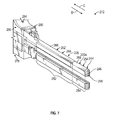
- Figure 7 is a perspective view of a portion of the electrical connector 212 of the electrical connector assembly 210.
- One or more of the electrical contacts 222 of the electrical connector 212 is a sense pin 222a that is configured to indicate when the electrical connectors 212 and 214 are de-mated by more than a predetermined de-mating distance.
- the sense pin 222a includes a mating segment 228 that extends a length, which includes a tip 244 having a tip surface 246.
- the tip 244 optionally includes one or more guide features, such as, but not limited to, a chamfer, a round, a fillet, and/or the like. In the exemplary embodiment of the sense pin 222a, the tip 244 includes a chamfer 248.
- the length of the mating segment 228 of the sense pin 222a includes an intermediate segment 252 and a tip segment 254.
- the tip segment 254 includes the tip 244 of the sense pin 222a.
- the tip segment 254 extends between the intermediate segment 252 and the tip 244 along the length of the mating segment 228 of the sense pin 222a. Accordingly, the intermediate segment 252 is offset from the tip 244 along the length of the mating segment 228 of the sense pin 222a in the direction of the arrow C. Because the tip 244 includes the entirety of the chamfer 248 and the intermediate segment 252 is offset from the tip 244, the intermediate segment 252 is offset (in the direction C) from the chamfer 248 along the length of the mating segment 228 of the sense pin 222a.
- the intermediate segment 252 and the tip segment 254 include respective surface materials 266 and 268.
- the surface material 266 of the intermediate segment 252 is defined by an extension 288 of the electrically non-conductive body 284 of the contact module 276 of the electrical connector 212.
- the extension 288 of the body 284 extends outward along the length of the mating segment 228 in the direction of the arrow D from a main segment 290 of the body 284 that extends over the lead frame 280.
- the surface material 266 of the intermediate segment 252 is electrically non-conductive such that the intermediate segment 252 is electrically non-conductive.
- the surface material 268 of the tip segment 254 is electrically conductive in the exemplary embodiment of the sense pin 222a. Operation of the sense pin 222a to indicate when the electrical connectors 212 and 214 are de-mated by more than the predetermined de-mating distance is substantially similar to the sense pin 22a ( Figures 1-3 ) and therefore will not be described in more detail herein.
- the intermediate segment 252 may be considered, and referred to herein, as a "sensing segment" of the sense pin 222a.
- FIG 8 is a cross-sectional view of another exemplary embodiment of an electrical connector assembly 310.
- the electrical connector assembly 310 includes electrical connectors 312 and 314 that are configured to mate together along a connection axis 316.
- the electrical connectors 312 and 314 include respective housings 318 and 320 and respective electrical contacts 322 and 324.
- the electrical contacts 224 of the electrical connector 214 may be referred to herein as "mating contacts”.
- the electrical connector 214 may be referred to herein as a "mating connector”.
- the electrical connector 312 includes one or more differential pairs 392 of sense pins 322aa and 322ab configured to indicate when the electrical connectors 312 and 314 are de-mated by more than a predetermined de-mating distance PDD 2 ( Figure 9 ).
- the sense pins 322aa and 322ab of the differential pair 392 include mating segments 328 that are configured to mate with corresponding electrical contacts 324aa and 324ab of the electrical connector 314.
- the sense pin 322aa and/or the sense pin 322ab include a bridging spring 394. In the exemplary embodiment of the electrical connector 312, only the sense pin 322aa includes a bridging spring 394. But, it should be understood that the sense pin 322ab may include a bridging spring 394 in addition or alternative to the sense pin 322aa.
- the bridging spring 394 is biased to an extended position shown in Figure 9 .
- the bridging spring 394 is configured to physically contact the other sense pin 322ab of the differential pair 392 to electrically connect the sense pins 322aa and 322ab together, as will be described below.
- Figure 8 illustrates the electrical connectors 312 and 314 as fully mated together.
- the bridging spring 394 is held in a retracted position against the natural bias of the bridging spring 394 to the extended position. In the retracted position, the bridging spring 394 is disengaged from (i.e., not in physical contact with) the other sense pin 322ab of the differential pair 392.
- a segment 396 of the housing 320 of the electrical connector 314 is engaged in physical contact with the bridging spring 394 to hold the bridging spring 394 in the retracted position.
- the segment 396 of the housing 320 engages the bridging spring 394 as the connectors 312 and 314 are mated together to move the bridging spring 394 from the extended position to the retracted position against the natural bias of the bridging spring 394.
- the housing segment 396 is divider that separates two adjacent mating receptacles 330 of the housing 320. But, the segment 396 may additionally or alternatively be any other segment of the housing 320.
- Figure 9 is a cross-sectional view of the electrical connector assembly 310 illustrating the electrical connectors 312 and 314 as partially de-mated from each other. Specifically, the electrical connectors 312 and 314 are de-mated by slightly more than the predetermined de-mating distance PDD 2 .
- the predetermined de-mating distance PDD 2 may be a distance beyond which the electrical performance of the electrical connector assembly 310 begins to degrade.
- a tip 398 of the bridging spring 394 clears the segment 396 of the housing 320.
- the natural bias of the bridging spring 394 moves the bridging spring 394 from the retracted position toward the extended position.
- the tip 398 of the bridging spring 394 is moved into physical contact with the other sense pin 322ab of the differential pair 392.
- the physical contact between the tip 398 of the bridging spring 394 and the other sense pin 322ab closes an electrical connection between the sense pins 322aa and 322ab of the differential pair 392, which indicates that the electrical contacts 322 of the electrical connector 312 are de-mated from the corresponding electrical contacts 324 of the electrical connector 314 by more than the predetermined de-mating distance PDD 2 .
- the embodiments described and/or illustrated herein may provide a sense pin having a more precise detection range, as compared to at least some known sense pins, for reliably indicating whether a mated pair of electrical connectors have been de-mated beyond a predetermined de-mating distance.
- the embodiments described and/or illustrated herein may offset the sensing segment of a sense pin from a guide feature of the sense pin.
- the embodiments described and/or illustrated herein may reduce or eliminate an unreliable segment of wipe length from the sensing segment of the sense pin. In other words, and for example, the embodiments described and/or illustrated herein may move the sensing segment of a sense pin to a segment of the wipe length that provides a more reliable electrical connection.
- the embodiments described and/or illustrated herein may reduce or eliminate false indications that the electrical contacts of an electrical connector assembly are still within a predetermined de-mating distance beyond which electrical performance degrades, which may prevent the electrical connector assembly from being unknowingly operated with degraded electrical performance.
- the embodiments described and/or illustrated herein may reduce or eliminate false indications that the electrical contacts of an electrical connector assembly are de-mated beyond a predetermined de-mating distance, which may prevent unnecessary diversion of the functionality of the electrical connector assembly to other resources.
Landscapes
- Engineering & Computer Science (AREA)
- Microelectronics & Electronic Packaging (AREA)
- Manufacturing & Machinery (AREA)
- Details Of Connecting Devices For Male And Female Coupling (AREA)
Abstract
Description
- The invention relates to an electrical connector having a sense pin.
- As a mated pair of electrical connectors are de-mated (i.e., separated) from each other, the electrical contacts of the electrical connectors may remain engaged in physical and electrical contact before the electrical connectors are fully de-mated from each other. For some known electrical connector assemblies, the electrical performance of the assembly will degrade when the electrical connectors are de-mated beyond a de-mating distance that is less than the fully de-mated distance. For example, the amount of electrical power and/or the speed, strength, and/or number of electrical signals transmitted through the assembly may be reduced.
- Some electrical connector assemblies include sense pins for indicating whether the electrical contacts of a mated pair of electrical connectors have achieved a predetermined wipe length that provides a reliable electrical connection between corresponding electrical contacts. Such known sense pins could be used to detect whether the mated pair of electrical connectors have been de-mated beyond a distance at which the electrical performance of the assembly begins to degrade. But, the detection range of known sense pins is too broad. For example, the tips of known sense pins include guide features such as chamfers, fillets, and/or rounds that guide initial engagement between the sense pin and the corresponding electrical contact of the other electrical connector. Tolerance stack ups between the guide features and the corresponding electrical contact create an unreliable segment of the wipe length wherein the electrical connection between the sense pin and the corresponding electrical contact is intermittent. The unreliable segment of the wipe length may cause the sense pin to falsely indicate that the electrical contacts are still within a predetermined de-mating distance beyond which electrical performance degrades. Such a false indication may cause the electrical connector assembly to be unknowingly operated with degraded electrical performance. The unreliable segment of the wipe length may also cause the sense pin to falsely indicate that the electrical contacts are de-mated beyond the predetermined de-mating distance, which may cause the unnecessary diversion of the functionality of the electrical connector assembly to other resources.
- A need remains for an electrical connector having a sense pin that provides a more precise detection range for reliably indicating whether a mated pair of electrical connectors have been de-mated beyond a predetermined de-mating distance.
- There is therefore provided an electrical connector according to the appended claim 1.
- According to the invention, an electrical connector comprises a housing and electrical contacts held by the housing. The electrical contacts are configured to mate with corresponding mating contacts of a mating connector. The housing holds a sense pin that is configured to mate with a corresponding mating contact of the mating connector. The sense pin extends a length that includes a tip segment and a sensing segment having respective different electrical characteristics. The tip segment extends from the sensing segment to a tip of the sense pin such that the sensing segment is offset from the tip along the length of the sense pin. The sensing segment is configured to indicate that the electrical contacts and the mating contacts are de-mated by more than a predetermined de-mating distance.
- Embodiments of the invention will now be described by way of example with reference to the accompanying drawings wherein:
-
Figure 1 is a cross-sectional view of an exemplary embodiment of an electrical connector assembly. -
Figure 2 is an elevational view of an exemplary embodiment of a sense pin of the electrical connector assembly shown inFigure 1 . -
Figure 3 is a cross-sectional view of the electrical connector assembly shown inFigure 1 illustrating the electrical connectors of the assembly as partially de-mated from each other. -
Figure 4 is a cross-sectional view of another exemplary embodiment of an electrical connector assembly. -
Figure 5 is a cross-sectional view of the electrical connector assembly shown inFigure 4 illustrating the electrical connectors of the assembly as partially de-mated from each other. -
Figure 6 is an elevational view of a portion of another exemplary embodiment of an electrical connector assembly. -
Figure 7 is a perspective view of a portion of an exemplary embodiment of an electrical connector of the electrical connector assembly shown inFigure 6 . -
Figure 8 is a cross-sectional view of another exemplary embodiment of an electrical connector assembly. -
Figure 9 is a cross-sectional view of the electrical connector assembly shown inFigure 8 illustrating the electrical connectors of the assembly as partially de-mated from each other. -
Figure 1 is a cross-sectional view of an exemplary embodiment of anelectrical connector assembly 10. Theelectrical connector assembly 10 includeselectrical connectors connection axis 16. Theelectrical connectors respective housings electrical contacts electrical connectors electrical contacts 22 of theelectrical connector 12 are mated with correspondingelectrical contacts 24 of theelectrical connector 14, thereby establishing an electrical connection between theelectrical connectors electrical contacts 22 of theelectrical connector 12 is asense pin 22a that is configured to indicate when theelectrical connectors Figure 3 ). - The
electrical contacts 22 of theelectrical connector 12 are held by thehousing 18 of theelectrical connector 12. Specifically, theelectrical contacts 22 includebases 26 andmating segments 28 that extend from thebases 26. In the exemplary embodiment of theelectrical connector 12, thebases 26 are held by thehousing 18 and thehousing 18 is configured such that themating segments 28 extend withincorresponding mating receptacles 30 of thehousing 18. In addition or alternatively, one or more of themating segments 28 extends outward from amating end 32 of thehousing 18, whether or not the mating segment(s) 28 is configured to be received within a corresponding mating receptacle (not shown) of theelectrical connector 14. - The
electrical contacts 24 of theelectrical connector 14 includebases 34 andmating segments 36 that extend from thebases 34. Thebases 34 of theelectrical contacts 24 are held by thehousing 20 and thehousing 20 is configured such that themating segments 36 extend outward from amating end 38 of thehousing 20 for being received within one or morecorresponding mating receptacles 30 of theelectrical connector 12. In addition or alternatively, one or more of themating segments 36 extends outward from themating end 38 but is not configured to be received within acorresponding mating receptacle 30 of theelectrical connector 12. Moreover, in addition or alternatively to includingmating segments 36 that extend outward from themating end 38, themating segment 36 of one or moreelectrical contacts 24 extends within a corresponding mating receptacle (not shown) of thehousing 20 for mating with the correspondingelectrical contact 22 within the mating receptacle. Theelectrical contacts 24 of theelectrical connector 14 may be referred to herein as "mating contacts". Theelectrical connector 14 may be referred to herein as a "mating connector". - The
electrical connectors Figure 1 in a fully mated position. To mate theelectrical connectors Figure 1 , thehousings connection axis 16. As theconnectors electrical contacts 22 of theelectrical connector 12 mate with theelectrical contacts 24 of theelectrical connector 14. Specifically, themating segments 28 of theelectrical contacts 22 move into physical contact with themating segments 36 of the correspondingelectrical contacts 24 of theelectrical connector 14. As theconnectors Figure 1 , themating segments 28 slide along thecorresponding mating segments 36, in physical contact therewith, until themating segments Figure 1 . The physical contact between themating segments mating segments electrical contacts corresponding mating segments electrical connector assembly 10, theelectrical contacts 24 of theelectrical connector 14 mate with theelectrical contacts 22 of theelectrical connector 12 within thecorresponding mating receptacles 30 of theelectrical connector 12. - The
electrical contacts mating segments electrical contacts corresponding mating segments mating segments mating segments mating segments - Although shown as abutting in the fully mated position shown in
Figure 1 , the mating ends 32 and 38 of thehousings electrical connectors mating end 32 of thehousing 18 is received into a receptacle (not shown) of themating end 38 of thehousing 20, or vice versa, when theelectrical connectors electrical connectors electrical contacts electrical connector 12 may include any number of themating receptacles 30, each of which may hold any number ofmating segments 28 and may receive any number ofmating segments 36 therein. Eachelectrical contact 22 and eachelectrical contact 24 may be any type of electrical contact, such as, but not limited to, a signal contact, a ground contact, an electrical power contact, a sense contact, and/or the like. - As briefly described above and will be described in more detail below, one or more of the
electrical contacts 22 of theelectrical connector 12 is asense pin 22a that is configured to indicate when theelectrical connectors sense pin 22a is configured to mate with a correspondingelectrical contact 24a of theelectrical connector 14.Figure 2 is an elevational view of an exemplary embodiment of a portion of thesense pin 22a. The base 26 (Figure 1 ) of thesense pin 22a is not shown inFigure 2 . Rather, only themating segment 28 of thesense pin 22a is shown inFigure 2 for clarity. Themating segment 28 of thesense pin 22a extends a length L along a centrallongitudinal axis 40 from anend 42 of themating segment 28 to atip 44 of thesense pin 22a. Thetip 44 includes atip surface 46. Thetip 44 optionally includes one or more guide features such as, but not limited to, a chamfer, a round, a fillet, and/or the like. In the exemplary embodiment of thesense pin 22a, thetip 44 includes achamfer 48. - The length L of the
mating segment 28 of thesense pin 22a includes abase segment 50, anintermediate segment 52, and atip segment 54. Specifically, thebase segment 50 extends a length L1 from thebase 26 of thesense pin 22a to anend 56 of thebase segment 50. Thebase segment 50 includes theend 42 of themating segment 28 of thesense pin 22a. Theend 42 defines an end of thebase segment 50 that is opposite theend 56. Theintermediate segment 52 extends a length L2 from anend 58 to anopposite end 60. Theend 58 of theintermediate segment 52 extends from theend 56 of thebase segment 50. The length L2 of theintermediate segment 52 extends from theend 56 of thebase segment 50 to thetip segment 54. In other words, theintermediate segment 52 extends between thebase segment 50 and thetip segment 54 along the length L of themating segment 28 of thesense pin 22a. - The
tip segment 54 includes thetip 44 of thesense pin 22a. Thetip segment 54 extends a length L3 from anend 62 to thetip 44, and more specifically from theend 62 to thetip surface 46. Theend 62 of thetip segment 54 extends from theend 60 of theintermediate segment 52. As can be seen inFigure 2 , thetip segment 54 extends between theintermediate segment 52 and thetip 44 along the length L of themating segment 28 of thesense pin 22a. Accordingly, theintermediate segment 52 is displaced by an offset O from thetip 44 along the length L of themating segment 28 of thesense pin 22a in the direction of the arrow A. Because thetip 44 includes the entirety of thechamfer 48 and theintermediate segment 52 is offset from thetip 44, theintermediate segment 52 is displaced by an offset O (in the direction A) from thechamfer 48 along the length L of themating segment 28 of thesense pin 22a. The offset O may have any positive, non-zero, value. - In the exemplary embodiment of the
sense pin 22a, thetip 44 extends a length that extends from anend 64 of thechamfer 48 to thetip surface 46. In other words, theend 64 of thechamfer 48 defines an interior end of thetip 44. Accordingly, in the exemplary embodiment of thesense pin 22a, theintermediate segment 52 is offset from both thechamfer 48 and thetip 44 by the same offset O (i.e., by the same distance). In embodiments wherein theend 64 of thechamfer 48 is not considered to define the interior end of the tip 44 (i.e., the length of thetip 44 is considered to extend past theend 64 of thechamfer 48 in the direction A), theintermediate segment 52 will be offset (in the direction A) from the interior end of thetip 44 and from theend 64 of thechamfer 48 by different distances. In such embodiments wherein theend 64 does not define the interior end of thetip 44, theintermediate segment 52 may be offset (in the direction A) from the interior end of thetip 44 by any positive, non-zero, distance and may be offset (in the direction A) from theend 64 of thechamfer 48 by any positive, non-zero, distance. It should be understood that in embodiments wherein thetip 44 includes another guide feature in addition or alternatively to thechamfer 48, theintermediate segment 52 will be offset from the other guide feature in a substantially similar manner to the offsets from thechamfer 48 described and/or illustrated herein (e.g., the offset O). - The
intermediate segment 52 and thetip segment 54 includerespective surface materials 66 and 68. Thesurface materials 66 and 68 have different electrical characteristics such that theintermediate segment 52 and thetip segment 54 have different electrical characteristics. Specifically, one of thesegments other segment sense pin 22a, the surface material 66 of theintermediate segment 52 is electrically non-conductive such that theintermediate segment 52 is electrically non-conductive, while thesurface material 68 of thetip segment 54 is electrically conductive such that thetip segment 54 is electrically conductive. - The surface materials 66 may be formed in any manner. For example, in some embodiments, the
mating segment 28 of thesense pin 22a is defined by abody 70 that is electrically conductive and the surface material 66 of theintermediate segment 52 is defined by an electrically non-conductive coating that is formed on thebody 70. In such embodiments wherein thebody 70 is electrically conductive, the electricallyconductive surface material 68 of thetip segment 54 may be defined by a surface of thebody 70 or may be defined by an electrically conductive coating that is formed on thebody 70. Moreover, and for example, in some embodiments thebody 70 is electrically non-conductive and thesurface material 68 of thetip segment 54 is defined by an electrically conductive coating that is formed on thebody 70. In such embodiments wherein thebody 70 is electrically non-conductive, the electrically non-conductive surface material 66 of theintermediate segment 52 may be defined by a surface of thebody 70 or may be defined by an electrically non-conductive coating that is formed on thebody 70. The surface material 66, thesurface material 68, and thebody 70 may each be fabricated from any material(s) that provide the surface material 66, thesurface material 68, and thebody 70 with the electrical characteristics described and/or illustrated herein. - As briefly described above, the
sense pin 22a is configured to indicate when theelectrical connectors Figure 1 , theintermediate segment 52 of thesense pin 22a is in physical contact with the correspondingelectrical contact 24a when theelectrical connectors intermediate segment 52 is in physical contact with theelectrical contact 24a at one ormore contact regions 74 of theelectrical contact 24a when theelectrical connectors electrical connectors connectors connection axis 16. -
Figure 3 is a cross-sectional view of theelectrical connector assembly 10 illustrating theelectrical connectors electrical connectors Figure 3 . The predetermined de-mating distance PDD may be a distance beyond which the electrical performance of theelectrical connector assembly 10 begins to degrade. Specifically, as theelectrical connectors Figure 1 , theelectrical contacts 22 of theelectrical connector 12 remain electrically connected to the correspondingelectrical contacts 24 of theelectrical connector 14 until theelectrical connectors Figure 1 ). Once theelectrical connectors electrical contacts 22 are disengaged from physical contact with the correspondingelectrical contacts 24 such that there is no electrical connection between theelectrical contacts electrical connectors electrical connectors electrical contacts 22 may remain electrically connected to the correspondingelectrical contacts 24, although the electrical performance of theelectrical connector assembly 10 will begin to degrade. For example, electrical performance degradation of theelectrical connector assembly 10 may include, but is not limited to, a reduction in the speed, quality, strength, amount, number, and/or the like of electrical signals transmitted through theassembly 10, a reduction in the speed, quality, strength, amount, and/or the like of electrical power transmitted through theassembly 10, and/or the like. - In the exemplary embodiment of the
electrical connector assembly 10, the predetermined de-mating distance PDD is the de-mating distance beyond which the electrical performance of theelectrical connector assembly 10 begins to degrade. In other words, the predetermined de-mating distance PDD is the upper limit of the de-mating distance before the performance of theelectrical connector assembly 10 begins to degrade. It should be appreciated that because theelectrical contacts electrical contacts - As the
connectors connection axis 16 from the fully mated position shown inFigure 1 toward the partially de-mated position shown inFigure 3 , thecontact regions 74 of theelectrical contact 24a slide along, in physical contact with, theintermediate segment 52 of thesense pin 22a. The transition between theintermediate segment 52 and thetip segment 54 is positioned along the length L of thesense pin 22a at a position that corresponds to the predetermined de-mating distance PDD. Specifically, theend 60 of theintermediate segment 52 is positioned along the length L (Figure 2 ) of themating segment 28 of thesense pin 22a such that theintermediate segment 52 is moved out of physical contact with (i.e., disengaged from) thecontact regions 74 of theelectrical contact 24a as thesense pin 22a and theelectrical contact 24a are de-mated beyond the predetermined de-mating distance PDD. Similarly, theend 62 of thetip segment 54 is positioned along the length L of themating segment 28 of thesense pin 22a such that thetip segment 54 is moved into physical contact with thecontact regions 74 of theelectrical contact 24a as thesense pin 22a and theelectrical contact 24a are de-mated beyond the predetermined de-mating distance PDD. - The
electrical connectors Figure 3 as being de-mated by slightly more than the predetermined de-mating distance PDD. Specifically, thecontact regions 74 of theelectrical contact 24a are engaged in physical contact with thetip segment 54 of thesense pin 22a but are disengaged from theintermediate segment 52 of thesense pin 22a. In the exemplary embodiment of theelectrical connector assembly 10, the physical contact between thecontact regions 74 of theelectrical contact 24a and the electricallyconductive surface material 68 of thetip segment 54 closes an electrical connection between thesense pin 22a and theelectrical contact 24a. The closing of the electrical connection indicates that theelectrical contacts 22 of theelectrical connector 12 are de-mated from the correspondingelectrical contacts 24 of theelectrical connector 14 by more than the predetermined de-mating distance PDD. Accordingly, theintermediate segment 52 is configured to indicate that theelectrical contacts contact regions 74 of theelectrical contact 24a. Specifically, as thecontact regions 74 cross the transition between theintermediate segment 52 and thetip segment 54, thecontact regions 74 disengage from physical contact with theintermediate segment 52 and engage in physical contact with thetip segment 54 to thereby close the electrical connection between thesense pin 22a and theelectrical contact 24a. The base 26 (Figure 1 ) of thesense pin 22a may be operatively connected to a processor, logic, controller, computer, circuit, and/or like for receiving and processing the indication (i.e., the closing of the electrical connection) from thesense pin 22a. - Because the
intermediate segment 52 of thesense pin 22a is configured to indicate that theelectrical contacts contact regions 74 of theelectrical contact 24a, theintermediate segment 52 may be considered, and referred to herein, as a "sensing segment" of thesense pin 22a. -
Figure 4 is a cross-sectional view of another exemplary embodiment of anelectrical connector assembly 110. Theelectrical connector assembly 110 includeselectrical connectors connection axis 116. Theelectrical connectors respective housings electrical contacts electrical contacts 122 of theelectrical connector 112 is asense pin 122a that is configured to indicate when theelectrical connectors Figure 5 ). Theelectrical contacts 124 of theelectrical connector 114 may be referred to herein as "mating contacts". Theelectrical connector 114 may be referred to herein as a "mating connector". - The
sense pin 122a includes amating segment 128 that extends a length from anend 142 of themating segment 128 to a tip 144 of thesense pin 122a. The tip 144 includes atip surface 146. The tip 144 optionally includes one or more guide features, such as, but not limited to, a chamfer, a round, a fillet, and/or the like. In the exemplary embodiment of thesense pin 122a, the tip 144 includes achamfer 148. The length of themating segment 128 of thesense pin 122a includes abase segment 150, anintermediate segment 152, and atip segment 154. Theintermediate segment 152 extends a length from anend 158 to anopposite end 160. Theintermediate segment 152 extends between thebase segment 150 and thetip segment 154 along the length of themating segment 128 of thesense pin 122a. - The
tip segment 154 includes the tip 144 of thesense pin 122a. Thetip segment 154 extends a length from anend 162 to the tip 144, and more specifically from theend 162 to thetip surface 146. Thetip segment 154 extends between theintermediate segment 152 and the tip 144 along the length of themating segment 128 of thesense pin 122a. Accordingly, theintermediate segment 152 is offset from the tip 144 along the length of themating segment 128 of thesense pin 122a in the direction of the arrow B. Because the tip 144 includes the entirety of thechamfer 148 and theintermediate segment 152 is offset from the tip 144, theintermediate segment 152 is offset (in the direction B) from thechamfer 148 along the length of themating segment 128 of thesense pin 122a. - The
intermediate segment 152 and thetip segment 154 includerespective surface materials sense pin 122a, thesurface material 166 of theintermediate segment 152 is electrically conductive such that theintermediate segment 152 is electrically conductive, while thesurface material 168 of thetip segment 154 is electrically non-conductive such that thetip segment 54 is electrically non-conductive. - As can be seen in
Figure 4 , theintermediate segment 152 of thesense pin 122a is in physical contact with the correspondingelectrical contact 124a of theelectrical connector 114 when theelectrical connectors intermediate segment 152 is in physical contact with theelectrical contact 124a at one ormore contact regions 174 of theelectrical contact 124a when theelectrical connectors -
Figure 5 is a cross-sectional view of theelectrical connector assembly 110 illustrating theelectrical connectors electrical connectors Figure 5 . The predetermined de-mating distance PDD1 may be a distance beyond which the electrical performance of theelectrical connector assembly 110 begins to degrade. - The transition between the
intermediate segment 152 and thetip segment 154 is positioned along the length of thesense pin 122a at a position that corresponds to the predetermined de-mating distance PDD1. As theconnectors connection axis 116 from the fully mated position shown inFigure 4 toward the partially de-mated position shown inFigure 5 , thecontact regions 174 of theelectrical contact 124a slide along, in physical contact with, theintermediate segment 152 of thesense pin 122a. As theconnectors intermediate segment 152 is moved out of physical contact with (i.e., disengaged from) thecontact regions 174 of theelectrical contact 124a and thetip segment 154 is moved into physical contact with thecontact regions 174. Theelectrical connectors Figure 5 as being de-mated by slightly more than the predetermined de-mating distance PDD1. - The physical contact between the
contact regions 174 of theelectrical contact 124a and the electricallynon-conductive surface material 168 of thetip segment 154 opens an electrical connection between thesense pin 122a and theelectrical contact 124a. The opening of the electrical connection indicates that theelectrical contacts 122 of theelectrical connector 112 are de-mated from the correspondingelectrical contacts 124 of theelectrical connector 114 beyond the predetermined de-mating distance PDD1. Accordingly, theintermediate segment 152 is configured to indicate that theelectrical contacts contact regions 174 of theelectrical contact 124a. Specifically, as thecontact regions 174 cross the transition between theintermediate segment 152 and thetip segment 154, thecontact regions 74 disengage from physical contact with theintermediate segment 52 and thereby open the electrical connection between thesense pin 122a and theelectrical contact 124a. - Because the
intermediate segment 152 of thesense pin 122a is configured to indicate that theelectrical contacts contact regions 174 of theelectrical contact 124a, theintermediate segment 152 may be considered, and referred to herein, as a "sensing segment" of thesense pin 122a. -
Figure 6 is an elevational view of another exemplary embodiment of anelectrical connector assembly 210. Theelectrical connector assembly 210 includeselectrical connectors connection axis 216. Theelectrical connectors electrical contacts electrical connector respective contact modules contact module respective lead frame non-conductive body lead frame non-conductive body 284 and/or 286 is an overmold that is molded over therespective lead frame 280 and/or 282. Thecontact modules electrical contacts electrical contacts 224 are arranged in differential pairs and/or the electrical contacts 226 are arranged in differential pairs. Theelectrical contacts 224 of theelectrical connector 214 may be referred to herein as "mating contacts". Theelectrical connector 214 may be referred to herein as a "mating connector". Thebodies electrical connector -
Figure 7 is a perspective view of a portion of theelectrical connector 212 of theelectrical connector assembly 210. One or more of theelectrical contacts 222 of theelectrical connector 212 is asense pin 222a that is configured to indicate when theelectrical connectors sense pin 222a includes amating segment 228 that extends a length, which includes atip 244 having atip surface 246. Thetip 244 optionally includes one or more guide features, such as, but not limited to, a chamfer, a round, a fillet, and/or the like. In the exemplary embodiment of thesense pin 222a, thetip 244 includes achamfer 248. The length of themating segment 228 of thesense pin 222a includes anintermediate segment 252 and atip segment 254. Thetip segment 254 includes thetip 244 of thesense pin 222a. Thetip segment 254 extends between theintermediate segment 252 and thetip 244 along the length of themating segment 228 of thesense pin 222a. Accordingly, theintermediate segment 252 is offset from thetip 244 along the length of themating segment 228 of thesense pin 222a in the direction of the arrow C. Because thetip 244 includes the entirety of thechamfer 248 and theintermediate segment 252 is offset from thetip 244, theintermediate segment 252 is offset (in the direction C) from thechamfer 248 along the length of themating segment 228 of thesense pin 222a. - The
intermediate segment 252 and thetip segment 254 includerespective surface materials 266 and 268. As can be seen inFigure 7 , thesurface material 266 of theintermediate segment 252 is defined by anextension 288 of the electricallynon-conductive body 284 of thecontact module 276 of theelectrical connector 212. Specifically, theextension 288 of thebody 284 extends outward along the length of themating segment 228 in the direction of the arrow D from amain segment 290 of thebody 284 that extends over thelead frame 280. Accordingly, in the exemplary embodiment of thesense pin 222a, thesurface material 266 of theintermediate segment 252 is electrically non-conductive such that theintermediate segment 252 is electrically non-conductive. The surface material 268 of thetip segment 254 is electrically conductive in the exemplary embodiment of thesense pin 222a. Operation of thesense pin 222a to indicate when theelectrical connectors sense pin 22a (Figures 1-3 ) and therefore will not be described in more detail herein. Theintermediate segment 252 may be considered, and referred to herein, as a "sensing segment" of thesense pin 222a. -
Figure 8 is a cross-sectional view of another exemplary embodiment of anelectrical connector assembly 310. Theelectrical connector assembly 310 includeselectrical connectors connection axis 316. Theelectrical connectors respective housings electrical contacts electrical contacts 224 of theelectrical connector 214 may be referred to herein as "mating contacts". Theelectrical connector 214 may be referred to herein as a "mating connector". - The
electrical connector 312 includes one or moredifferential pairs 392 of sense pins 322aa and 322ab configured to indicate when theelectrical connectors Figure 9 ). The sense pins 322aa and 322ab of thedifferential pair 392 includemating segments 328 that are configured to mate with corresponding electrical contacts 324aa and 324ab of theelectrical connector 314. The sense pin 322aa and/or the sense pin 322ab include abridging spring 394. In the exemplary embodiment of theelectrical connector 312, only the sense pin 322aa includes abridging spring 394. But, it should be understood that the sense pin 322ab may include abridging spring 394 in addition or alternative to the sense pin 322aa. - The bridging
spring 394 is biased to an extended position shown inFigure 9 . In the extended position, the bridgingspring 394 is configured to physically contact the other sense pin 322ab of thedifferential pair 392 to electrically connect the sense pins 322aa and 322ab together, as will be described below.Figure 8 illustrates theelectrical connectors Figure 8 , the bridgingspring 394 is held in a retracted position against the natural bias of thebridging spring 394 to the extended position. In the retracted position, the bridgingspring 394 is disengaged from (i.e., not in physical contact with) the other sense pin 322ab of thedifferential pair 392. As can be seen inFigure 8 , asegment 396 of thehousing 320 of theelectrical connector 314 is engaged in physical contact with thebridging spring 394 to hold thebridging spring 394 in the retracted position. As should be apparent fromFigure 8 , thesegment 396 of thehousing 320 engages thebridging spring 394 as theconnectors bridging spring 394 from the extended position to the retracted position against the natural bias of thebridging spring 394. In the exemplary embodiment of theelectrical connector 314, thehousing segment 396 is divider that separates twoadjacent mating receptacles 330 of thehousing 320. But, thesegment 396 may additionally or alternatively be any other segment of thehousing 320. -
Figure 9 is a cross-sectional view of theelectrical connector assembly 310 illustrating theelectrical connectors electrical connectors electrical connector assembly 310 begins to degrade. - As the
connectors connection axis 316 from the fully mated position shown inFigure 8 toward the partially de-mated position shown inFigure 9 , atip 398 of thebridging spring 394 clears thesegment 396 of thehousing 320. As thebridging spring 394 continues to clear thesegment 396, the natural bias of thebridging spring 394 moves thebridging spring 394 from the retracted position toward the extended position. As theconnectors tip 398 of thebridging spring 394 is moved into physical contact with the other sense pin 322ab of thedifferential pair 392. The physical contact between thetip 398 of thebridging spring 394 and the other sense pin 322ab closes an electrical connection between the sense pins 322aa and 322ab of thedifferential pair 392, which indicates that theelectrical contacts 322 of theelectrical connector 312 are de-mated from the correspondingelectrical contacts 324 of theelectrical connector 314 by more than the predetermined de-mating distance PDD2. - The embodiments described and/or illustrated herein may provide a sense pin having a more precise detection range, as compared to at least some known sense pins, for reliably indicating whether a mated pair of electrical connectors have been de-mated beyond a predetermined de-mating distance. For example, the embodiments described and/or illustrated herein may offset the sensing segment of a sense pin from a guide feature of the sense pin. Moreover, and for example, the embodiments described and/or illustrated herein may reduce or eliminate an unreliable segment of wipe length from the sensing segment of the sense pin. In other words, and for example, the embodiments described and/or illustrated herein may move the sensing segment of a sense pin to a segment of the wipe length that provides a more reliable electrical connection.
- The embodiments described and/or illustrated herein may reduce or eliminate false indications that the electrical contacts of an electrical connector assembly are still within a predetermined de-mating distance beyond which electrical performance degrades, which may prevent the electrical connector assembly from being unknowingly operated with degraded electrical performance. The embodiments described and/or illustrated herein may reduce or eliminate false indications that the electrical contacts of an electrical connector assembly are de-mated beyond a predetermined de-mating distance, which may prevent unnecessary diversion of the functionality of the electrical connector assembly to other resources.
Claims (9)
- An electrical connector (12, 112, 212) for mating with a mating connector (14, 114), the electrical connector comprising a housing (18, 118) and electrical contacts (22, 122, 222) held by the housing, the electrical contacts being configured to mate with corresponding mating contacts (24, 124) of the mating connector, the electrical connector being characterized by:a sense pin (22a, 122a, 222a) held by the housing and configured to mate with a corresponding mating contact (24a, 124a) of the mating connector, the sense pin extending a length that includes a tip segment (54, 154, 254) and a sensing segment (52, 152, 252) having respective different electrical characteristics, the tip segment extending from the sensing segment to a tip (44, 144) of the sense pin such that the sensing segment is offset from the tip along the length of the sense pin, wherein the sensing segment is configured to indicate that the electrical contacts and the mating contacts are de-mated by more than a predetermined de-mating distance (PDD).
- The electrical connector (12, 112, 212) of claim 1, wherein the sensing segment (52, 152, 252) is in physical contact with the corresponding mating contact (24a, 124a) when the electrical connector is fully mated with the mating connector, and wherein the sensing segment is configured to indicate that the electrical contacts (22, 122, 222) and the mating contacts (24, 124) are de-mated by more than the predetermined de-mating distance (PDD) by disengaging from the corresponding mating contact (24a, 124a) as the electrical connector and the mating connector are de-mated.
- The electrical connector (12, 112, 212) of claim 1 or 2, wherein the sensing segment (52, 152, 252) is configured to indicate that the electrical contacts (22, 122, 222) and the mating contacts (24, 124) are de-mated by more than the predetermined de-mating distance (PDD) via the opening or closing of an electrical connection between the sense pin (22a, 122a, 222a) and the corresponding mating contact (24a, 124a).
- The electrical connector (12) of claim 1, 2, or 3, wherein the tip segment (54) of the sense pin (22a) has a conductive surface material such that the electrical characteristic of the tip segment is conductivity, and the sensing segment (52) of the sense pin has a non-conductive surface material such that the electrical characteristic of the sensing segment is non-conductivity.
- The electrical connector (112) of claim 1, 2, or 3, wherein the sensing segment (152) of the sense pin (122a) has a conductive surface material such that the electrical characteristic of the sensing segment is conductivity, and the tip segment (154) of the sense pin has a non-conductive surface material such that the electrical characteristic of the tip segment is non-conductivity.
- The electrical connector (212) of any preceding claim, further comprising a contact module (276) held by the housing, the contact module comprising a lead frame (280) and a non-conductive body (284) that extends over the lead frame, the electrical contacts (222) being held by the contact module, wherein the sensing segment (252) of the sense pin (222a) is defined by an extension (288) of the non-conductive body of the contact module.
- The electrical connector (12) of any preceding claim, wherein the predetermined de-mating distance (PDD) is a distance beyond which an electrical performance of the electrical and mating connectors (12, 14) begins to degrade.
- The electrical connector (12) of any preceding claim, wherein the predetermined de-mating distance (PDD) is less than a wipe length (WL) of the electrical contacts (22).
- The electrical connector (12) of any preceding claim, wherein the tip (44) comprises a guide feature (48) such that the sensing segment (52) is offset from the guide feature along the length of the sense pin (22a).
Applications Claiming Priority (1)
| Application Number | Priority Date | Filing Date | Title |
|---|---|---|---|
| US13/784,136 US8894435B2 (en) | 2013-03-04 | 2013-03-04 | Sense pin for an electrical connector |
Publications (2)
| Publication Number | Publication Date |
|---|---|
| EP2775571A1 true EP2775571A1 (en) | 2014-09-10 |
| EP2775571B1 EP2775571B1 (en) | 2017-04-26 |
Family
ID=50184780
Family Applications (1)
| Application Number | Title | Priority Date | Filing Date |
|---|---|---|---|
| EP14156945.9A Active EP2775571B1 (en) | 2013-03-04 | 2014-02-27 | Sense pin for an electrical connector |
Country Status (4)
| Country | Link |
|---|---|
| US (1) | US8894435B2 (en) |
| EP (1) | EP2775571B1 (en) |
| CN (1) | CN104037521B (en) |
| TW (1) | TWI593189B (en) |
Cited By (1)
| Publication number | Priority date | Publication date | Assignee | Title |
|---|---|---|---|---|
| EP4002606A1 (en) * | 2020-11-19 | 2022-05-25 | Rosenberger Hochfrequenztechnik GmbH & Co. KG | Electrical connector, connector and data transmission system |
Families Citing this family (3)
| Publication number | Priority date | Publication date | Assignee | Title |
|---|---|---|---|---|
| US10096924B2 (en) * | 2016-11-21 | 2018-10-09 | Te Connectivity Corporation | Header contact for header connector of a communication system |
| CN111504243B (en) * | 2019-01-31 | 2022-12-02 | 泰科电子(上海)有限公司 | Detection device and detection method suitable for detecting terminal assembly depth of cable connector |
| US12651872B2 (en) * | 2023-03-24 | 2026-06-09 | Samsung Electronics Co., Ltd. | Water detection method and electronic device performing the same |
Citations (5)
| Publication number | Priority date | Publication date | Assignee | Title |
|---|---|---|---|---|
| EP1455423A1 (en) * | 2003-02-14 | 2004-09-08 | Delphi Technologies, Inc. | Connector containing a short-circuit terminal |
| JP2006107863A (en) * | 2004-10-04 | 2006-04-20 | Nec Access Technica Ltd | Connector structure and connector connection abnormality detection device |
| US20110039445A1 (en) * | 2007-05-03 | 2011-02-17 | Boyd Garth W | Visual indicator of proper interconnection for an implanted medical device |
| DE102011050638A1 (en) * | 2010-06-10 | 2012-03-22 | Fanuc Corporation | connector |
| US20120081102A1 (en) * | 2010-09-30 | 2012-04-05 | Apple Inc. | Audio jack with ground detect |
Family Cites Families (1)
| Publication number | Priority date | Publication date | Assignee | Title |
|---|---|---|---|---|
| TW555253U (en) * | 2002-05-13 | 2003-09-21 | Delta Electronics Inc | Connector having signal detection function |
-
2013
- 2013-03-04 US US13/784,136 patent/US8894435B2/en active Active
-
2014
- 2014-02-27 EP EP14156945.9A patent/EP2775571B1/en active Active
- 2014-02-27 TW TW103106683A patent/TWI593189B/en active
- 2014-03-04 CN CN201410182682.2A patent/CN104037521B/en active Active
Patent Citations (5)
| Publication number | Priority date | Publication date | Assignee | Title |
|---|---|---|---|---|
| EP1455423A1 (en) * | 2003-02-14 | 2004-09-08 | Delphi Technologies, Inc. | Connector containing a short-circuit terminal |
| JP2006107863A (en) * | 2004-10-04 | 2006-04-20 | Nec Access Technica Ltd | Connector structure and connector connection abnormality detection device |
| US20110039445A1 (en) * | 2007-05-03 | 2011-02-17 | Boyd Garth W | Visual indicator of proper interconnection for an implanted medical device |
| DE102011050638A1 (en) * | 2010-06-10 | 2012-03-22 | Fanuc Corporation | connector |
| US20120081102A1 (en) * | 2010-09-30 | 2012-04-05 | Apple Inc. | Audio jack with ground detect |
Cited By (2)
| Publication number | Priority date | Publication date | Assignee | Title |
|---|---|---|---|---|
| EP4002606A1 (en) * | 2020-11-19 | 2022-05-25 | Rosenberger Hochfrequenztechnik GmbH & Co. KG | Electrical connector, connector and data transmission system |
| WO2022106553A1 (en) | 2020-11-19 | 2022-05-27 | Rosenberger Hochfrequenztechnik Gmbh & Co. Kg | Electrical plug-in connection, electrical connector and data transmission system |
Also Published As
| Publication number | Publication date |
|---|---|
| TWI593189B (en) | 2017-07-21 |
| CN104037521B (en) | 2018-07-17 |
| US8894435B2 (en) | 2014-11-25 |
| EP2775571B1 (en) | 2017-04-26 |
| TW201444197A (en) | 2014-11-16 |
| CN104037521A (en) | 2014-09-10 |
| US20140248792A1 (en) | 2014-09-04 |
Similar Documents
| Publication | Publication Date | Title |
|---|---|---|
| US9413108B2 (en) | Lever-actuated electrical connector and mating system | |
| US9136636B2 (en) | Connector | |
| EP3619778B1 (en) | Connector system | |
| US9160095B2 (en) | Connector assembly with connector position assurance stabilizer | |
| CN103004031B (en) | Plug-type connector having a radially acting latching device | |
| CN101257167B (en) | Connector and a connector assembly | |
| US9385473B2 (en) | Lever-actuated electrical connector and mating system | |
| EP2775571B1 (en) | Sense pin for an electrical connector | |
| US9178325B2 (en) | Low profile connector | |
| US20160372870A1 (en) | Electrical connector having improved terminal arrangement | |
| US9837771B2 (en) | Electrical connector with short circuit element | |
| US20200274280A1 (en) | Female terminal position assurance (tpa) device for a connector and method for assembling thereof | |
| US10033126B2 (en) | Connector | |
| US20170279222A1 (en) | Lever-type connector | |
| ATE373882T1 (en) | COAXIAL CONNECTOR AND ANTENNA ARRANGEMENT WITH A SWITCH FUNCTION | |
| EP3213375B1 (en) | Hermaphroditic electrical connector and method of manufacturing it | |
| US8460025B2 (en) | Detecting connector | |
| US7918676B2 (en) | Connector with a connection detecting function and with a force multiplying member | |
| WO2014017549A1 (en) | Connector | |
| US20110318971A1 (en) | Electrical connector assembly with anti-mismatching mating connectors | |
| US20130045620A1 (en) | Electrical connector with elastic locking mechnism and electrical connector assembly thereof | |
| EP3961823B1 (en) | Connector with a position assurance element having a contact receptacle | |
| US9225123B2 (en) | USB receptacle | |
| CN107809027B (en) | Connectors with short-circuit terminals | |
| CN201160179Y (en) | coaxial connector |
Legal Events
| Date | Code | Title | Description |
|---|---|---|---|
| PUAI | Public reference made under article 153(3) epc to a published international application that has entered the european phase |
Free format text: ORIGINAL CODE: 0009012 |
|
| 17P | Request for examination filed |
Effective date: 20140227 |
|
| AK | Designated contracting states |
Kind code of ref document: A1 Designated state(s): AL AT BE BG CH CY CZ DE DK EE ES FI FR GB GR HR HU IE IS IT LI LT LU LV MC MK MT NL NO PL PT RO RS SE SI SK SM TR |
|
| AX | Request for extension of the european patent |
Extension state: BA ME |
|
| R17P | Request for examination filed (corrected) |
Effective date: 20150220 |
|
| RBV | Designated contracting states (corrected) |
Designated state(s): AL AT BE BG CH CY CZ DE DK EE ES FI FR GB GR HR HU IE IS IT LI LT LU LV MC MK MT NL NO PL PT RO RS SE SI SK SM TR |
|
| REG | Reference to a national code |
Ref country code: DE Ref legal event code: R079 Ref document number: 602014008931 Country of ref document: DE Free format text: PREVIOUS MAIN CLASS: H01R0013641000 Ipc: H01R0013405000 |
|
| GRAP | Despatch of communication of intention to grant a patent |
Free format text: ORIGINAL CODE: EPIDOSNIGR1 |
|
| STAA | Information on the status of an ep patent application or granted ep patent |
Free format text: STATUS: GRANT OF PATENT IS INTENDED |
|
| RIC1 | Information provided on ipc code assigned before grant |
Ipc: H01R 13/641 20060101ALI20161109BHEP Ipc: H01R 13/66 20060101ALI20161109BHEP Ipc: H01R 107/00 20060101ALN20161109BHEP Ipc: H01R 13/703 20060101ALN20161109BHEP Ipc: H01R 43/24 20060101ALI20161109BHEP Ipc: H01R 13/405 20060101AFI20161109BHEP |
|
| INTG | Intention to grant announced |
Effective date: 20161129 |
|
| RAP1 | Party data changed (applicant data changed or rights of an application transferred) |
Owner name: TE CONNECTIVITY CORPORATION |
|
| GRAS | Grant fee paid |
Free format text: ORIGINAL CODE: EPIDOSNIGR3 |
|
| GRAA | (expected) grant |
Free format text: ORIGINAL CODE: 0009210 |
|
| STAA | Information on the status of an ep patent application or granted ep patent |
Free format text: STATUS: THE PATENT HAS BEEN GRANTED |
|
| AK | Designated contracting states |
Kind code of ref document: B1 Designated state(s): AL AT BE BG CH CY CZ DE DK EE ES FI FR GB GR HR HU IE IS IT LI LT LU LV MC MK MT NL NO PL PT RO RS SE SI SK SM TR |
|
| REG | Reference to a national code |
Ref country code: GB Ref legal event code: FG4D |
|
| REG | Reference to a national code |
Ref country code: CH Ref legal event code: EP |
|
| REG | Reference to a national code |
Ref country code: AT Ref legal event code: REF Ref document number: 888612 Country of ref document: AT Kind code of ref document: T Effective date: 20170515 |
|
| REG | Reference to a national code |
Ref country code: IE Ref legal event code: FG4D |
|
| REG | Reference to a national code |
Ref country code: DE Ref legal event code: R096 Ref document number: 602014008931 Country of ref document: DE |
|
| REG | Reference to a national code |
Ref country code: NL Ref legal event code: MP Effective date: 20170426 |
|
| REG | Reference to a national code |
Ref country code: LT Ref legal event code: MG4D |
|
| REG | Reference to a national code |
Ref country code: AT Ref legal event code: MK05 Ref document number: 888612 Country of ref document: AT Kind code of ref document: T Effective date: 20170426 |
|
| PG25 | Lapsed in a contracting state [announced via postgrant information from national office to epo] |
Ref country code: NL Free format text: LAPSE BECAUSE OF FAILURE TO SUBMIT A TRANSLATION OF THE DESCRIPTION OR TO PAY THE FEE WITHIN THE PRESCRIBED TIME-LIMIT Effective date: 20170426 |
|
| PG25 | Lapsed in a contracting state [announced via postgrant information from national office to epo] |
Ref country code: NO Free format text: LAPSE BECAUSE OF FAILURE TO SUBMIT A TRANSLATION OF THE DESCRIPTION OR TO PAY THE FEE WITHIN THE PRESCRIBED TIME-LIMIT Effective date: 20170726 Ref country code: AT Free format text: LAPSE BECAUSE OF FAILURE TO SUBMIT A TRANSLATION OF THE DESCRIPTION OR TO PAY THE FEE WITHIN THE PRESCRIBED TIME-LIMIT Effective date: 20170426 Ref country code: GR Free format text: LAPSE BECAUSE OF FAILURE TO SUBMIT A TRANSLATION OF THE DESCRIPTION OR TO PAY THE FEE WITHIN THE PRESCRIBED TIME-LIMIT Effective date: 20170727 Ref country code: HR Free format text: LAPSE BECAUSE OF FAILURE TO SUBMIT A TRANSLATION OF THE DESCRIPTION OR TO PAY THE FEE WITHIN THE PRESCRIBED TIME-LIMIT Effective date: 20170426 Ref country code: FI Free format text: LAPSE BECAUSE OF FAILURE TO SUBMIT A TRANSLATION OF THE DESCRIPTION OR TO PAY THE FEE WITHIN THE PRESCRIBED TIME-LIMIT Effective date: 20170426 Ref country code: ES Free format text: LAPSE BECAUSE OF FAILURE TO SUBMIT A TRANSLATION OF THE DESCRIPTION OR TO PAY THE FEE WITHIN THE PRESCRIBED TIME-LIMIT Effective date: 20170426 Ref country code: LT Free format text: LAPSE BECAUSE OF FAILURE TO SUBMIT A TRANSLATION OF THE DESCRIPTION OR TO PAY THE FEE WITHIN THE PRESCRIBED TIME-LIMIT Effective date: 20170426 |
|
| PG25 | Lapsed in a contracting state [announced via postgrant information from national office to epo] |
Ref country code: IS Free format text: LAPSE BECAUSE OF FAILURE TO SUBMIT A TRANSLATION OF THE DESCRIPTION OR TO PAY THE FEE WITHIN THE PRESCRIBED TIME-LIMIT Effective date: 20170826 Ref country code: BG Free format text: LAPSE BECAUSE OF FAILURE TO SUBMIT A TRANSLATION OF THE DESCRIPTION OR TO PAY THE FEE WITHIN THE PRESCRIBED TIME-LIMIT Effective date: 20170726 Ref country code: LV Free format text: LAPSE BECAUSE OF FAILURE TO SUBMIT A TRANSLATION OF THE DESCRIPTION OR TO PAY THE FEE WITHIN THE PRESCRIBED TIME-LIMIT Effective date: 20170426 Ref country code: RS Free format text: LAPSE BECAUSE OF FAILURE TO SUBMIT A TRANSLATION OF THE DESCRIPTION OR TO PAY THE FEE WITHIN THE PRESCRIBED TIME-LIMIT Effective date: 20170426 Ref country code: SE Free format text: LAPSE BECAUSE OF FAILURE TO SUBMIT A TRANSLATION OF THE DESCRIPTION OR TO PAY THE FEE WITHIN THE PRESCRIBED TIME-LIMIT Effective date: 20170426 Ref country code: PL Free format text: LAPSE BECAUSE OF FAILURE TO SUBMIT A TRANSLATION OF THE DESCRIPTION OR TO PAY THE FEE WITHIN THE PRESCRIBED TIME-LIMIT Effective date: 20170426 |
|
| REG | Reference to a national code |
Ref country code: FR Ref legal event code: PLFP Year of fee payment: 5 |
|
| REG | Reference to a national code |
Ref country code: DE Ref legal event code: R097 Ref document number: 602014008931 Country of ref document: DE |
|
| PG25 | Lapsed in a contracting state [announced via postgrant information from national office to epo] |
Ref country code: DK Free format text: LAPSE BECAUSE OF FAILURE TO SUBMIT A TRANSLATION OF THE DESCRIPTION OR TO PAY THE FEE WITHIN THE PRESCRIBED TIME-LIMIT Effective date: 20170426 Ref country code: RO Free format text: LAPSE BECAUSE OF FAILURE TO SUBMIT A TRANSLATION OF THE DESCRIPTION OR TO PAY THE FEE WITHIN THE PRESCRIBED TIME-LIMIT Effective date: 20170426 Ref country code: SK Free format text: LAPSE BECAUSE OF FAILURE TO SUBMIT A TRANSLATION OF THE DESCRIPTION OR TO PAY THE FEE WITHIN THE PRESCRIBED TIME-LIMIT Effective date: 20170426 Ref country code: CZ Free format text: LAPSE BECAUSE OF FAILURE TO SUBMIT A TRANSLATION OF THE DESCRIPTION OR TO PAY THE FEE WITHIN THE PRESCRIBED TIME-LIMIT Effective date: 20170426 Ref country code: EE Free format text: LAPSE BECAUSE OF FAILURE TO SUBMIT A TRANSLATION OF THE DESCRIPTION OR TO PAY THE FEE WITHIN THE PRESCRIBED TIME-LIMIT Effective date: 20170426 |
|
| PG25 | Lapsed in a contracting state [announced via postgrant information from national office to epo] |
Ref country code: SM Free format text: LAPSE BECAUSE OF FAILURE TO SUBMIT A TRANSLATION OF THE DESCRIPTION OR TO PAY THE FEE WITHIN THE PRESCRIBED TIME-LIMIT Effective date: 20170426 Ref country code: IT Free format text: LAPSE BECAUSE OF FAILURE TO SUBMIT A TRANSLATION OF THE DESCRIPTION OR TO PAY THE FEE WITHIN THE PRESCRIBED TIME-LIMIT Effective date: 20170426 |
|
| PLBE | No opposition filed within time limit |
Free format text: ORIGINAL CODE: 0009261 |
|
| STAA | Information on the status of an ep patent application or granted ep patent |
Free format text: STATUS: NO OPPOSITION FILED WITHIN TIME LIMIT |
|
| 26N | No opposition filed |
Effective date: 20180129 |
|
| PG25 | Lapsed in a contracting state [announced via postgrant information from national office to epo] |
Ref country code: SI Free format text: LAPSE BECAUSE OF FAILURE TO SUBMIT A TRANSLATION OF THE DESCRIPTION OR TO PAY THE FEE WITHIN THE PRESCRIBED TIME-LIMIT Effective date: 20170426 |
|
| REG | Reference to a national code |
Ref country code: CH Ref legal event code: PL |
|
| PG25 | Lapsed in a contracting state [announced via postgrant information from national office to epo] |
Ref country code: MC Free format text: LAPSE BECAUSE OF FAILURE TO SUBMIT A TRANSLATION OF THE DESCRIPTION OR TO PAY THE FEE WITHIN THE PRESCRIBED TIME-LIMIT Effective date: 20170426 |
|
| REG | Reference to a national code |
Ref country code: IE Ref legal event code: MM4A |
|
| REG | Reference to a national code |
Ref country code: BE Ref legal event code: MM Effective date: 20180228 |
|
| PG25 | Lapsed in a contracting state [announced via postgrant information from national office to epo] |
Ref country code: LI Free format text: LAPSE BECAUSE OF NON-PAYMENT OF DUE FEES Effective date: 20180228 Ref country code: LU Free format text: LAPSE BECAUSE OF NON-PAYMENT OF DUE FEES Effective date: 20180227 Ref country code: CH Free format text: LAPSE BECAUSE OF NON-PAYMENT OF DUE FEES Effective date: 20180228 |
|
| PG25 | Lapsed in a contracting state [announced via postgrant information from national office to epo] |
Ref country code: IE Free format text: LAPSE BECAUSE OF NON-PAYMENT OF DUE FEES Effective date: 20180227 |
|
| PG25 | Lapsed in a contracting state [announced via postgrant information from national office to epo] |
Ref country code: BE Free format text: LAPSE BECAUSE OF NON-PAYMENT OF DUE FEES Effective date: 20180228 |
|
| PG25 | Lapsed in a contracting state [announced via postgrant information from national office to epo] |
Ref country code: MT Free format text: LAPSE BECAUSE OF NON-PAYMENT OF DUE FEES Effective date: 20180227 |
|
| PG25 | Lapsed in a contracting state [announced via postgrant information from national office to epo] |
Ref country code: TR Free format text: LAPSE BECAUSE OF FAILURE TO SUBMIT A TRANSLATION OF THE DESCRIPTION OR TO PAY THE FEE WITHIN THE PRESCRIBED TIME-LIMIT Effective date: 20170426 |
|
| PG25 | Lapsed in a contracting state [announced via postgrant information from national office to epo] |
Ref country code: HU Free format text: LAPSE BECAUSE OF FAILURE TO SUBMIT A TRANSLATION OF THE DESCRIPTION OR TO PAY THE FEE WITHIN THE PRESCRIBED TIME-LIMIT; INVALID AB INITIO Effective date: 20140227 Ref country code: PT Free format text: LAPSE BECAUSE OF FAILURE TO SUBMIT A TRANSLATION OF THE DESCRIPTION OR TO PAY THE FEE WITHIN THE PRESCRIBED TIME-LIMIT Effective date: 20170426 |
|
| PG25 | Lapsed in a contracting state [announced via postgrant information from national office to epo] |
Ref country code: MK Free format text: LAPSE BECAUSE OF NON-PAYMENT OF DUE FEES Effective date: 20170426 Ref country code: CY Free format text: LAPSE BECAUSE OF FAILURE TO SUBMIT A TRANSLATION OF THE DESCRIPTION OR TO PAY THE FEE WITHIN THE PRESCRIBED TIME-LIMIT Effective date: 20170426 |
|
| PG25 | Lapsed in a contracting state [announced via postgrant information from national office to epo] |
Ref country code: AL Free format text: LAPSE BECAUSE OF FAILURE TO SUBMIT A TRANSLATION OF THE DESCRIPTION OR TO PAY THE FEE WITHIN THE PRESCRIBED TIME-LIMIT Effective date: 20170426 |
|
| REG | Reference to a national code |
Ref country code: GB Ref legal event code: 732E Free format text: REGISTERED BETWEEN 20250731 AND 20250806 |
|
| PGFP | Annual fee paid to national office [announced via postgrant information from national office to epo] |
Ref country code: FR Payment date: 20251231 Year of fee payment: 13 |
|
| PGFP | Annual fee paid to national office [announced via postgrant information from national office to epo] |
Ref country code: GB Payment date: 20260106 Year of fee payment: 13 |
|
| PGFP | Annual fee paid to national office [announced via postgrant information from national office to epo] |
Ref country code: DE Payment date: 20260102 Year of fee payment: 13 |