EP2775525A1 - High dynamic range pixel having a plurality of photodiodes with a single implant - Google Patents
High dynamic range pixel having a plurality of photodiodes with a single implant Download PDFInfo
- Publication number
- EP2775525A1 EP2775525A1 EP14157610.8A EP14157610A EP2775525A1 EP 2775525 A1 EP2775525 A1 EP 2775525A1 EP 14157610 A EP14157610 A EP 14157610A EP 2775525 A1 EP2775525 A1 EP 2775525A1
- Authority
- EP
- European Patent Office
- Prior art keywords
- integration photodiode
- photodiode
- exposure area
- light exposure
- implanted
- Prior art date
- Legal status (The legal status is an assumption and is not a legal conclusion. Google has not performed a legal analysis and makes no representation as to the accuracy of the status listed.)
- Withdrawn
Links
Images

Classifications
-
- H—ELECTRICITY
- H10—SEMICONDUCTOR DEVICES; ELECTRIC SOLID-STATE DEVICES NOT OTHERWISE PROVIDED FOR
- H10F—INORGANIC SEMICONDUCTOR DEVICES SENSITIVE TO INFRARED RADIATION, LIGHT, ELECTROMAGNETIC RADIATION OF SHORTER WAVELENGTH OR CORPUSCULAR RADIATION
- H10F39/00—Integrated devices, or assemblies of multiple devices, comprising at least one element covered by group H10F30/00, e.g. radiation detectors comprising photodiode arrays
- H10F39/10—Integrated devices
- H10F39/12—Image sensors
- H10F39/15—Charge-coupled device [CCD] image sensors
- H10F39/151—Geometry or disposition of pixel elements, address lines or gate electrodes
-
- H—ELECTRICITY
- H10—SEMICONDUCTOR DEVICES; ELECTRIC SOLID-STATE DEVICES NOT OTHERWISE PROVIDED FOR
- H10F—INORGANIC SEMICONDUCTOR DEVICES SENSITIVE TO INFRARED RADIATION, LIGHT, ELECTROMAGNETIC RADIATION OF SHORTER WAVELENGTH OR CORPUSCULAR RADIATION
- H10F39/00—Integrated devices, or assemblies of multiple devices, comprising at least one element covered by group H10F30/00, e.g. radiation detectors comprising photodiode arrays
- H10F39/011—Manufacture or treatment of image sensors covered by group H10F39/12
- H10F39/014—Manufacture or treatment of image sensors covered by group H10F39/12 of CMOS image sensors
-
- H—ELECTRICITY
- H10—SEMICONDUCTOR DEVICES; ELECTRIC SOLID-STATE DEVICES NOT OTHERWISE PROVIDED FOR
- H10F—INORGANIC SEMICONDUCTOR DEVICES SENSITIVE TO INFRARED RADIATION, LIGHT, ELECTROMAGNETIC RADIATION OF SHORTER WAVELENGTH OR CORPUSCULAR RADIATION
- H10F39/00—Integrated devices, or assemblies of multiple devices, comprising at least one element covered by group H10F30/00, e.g. radiation detectors comprising photodiode arrays
- H10F39/80—Constructional details of image sensors
- H10F39/802—Geometry or disposition of elements in pixels, e.g. address-lines or gate electrodes
- H10F39/8027—Geometry of the photosensitive area
-
- H—ELECTRICITY
- H04—ELECTRIC COMMUNICATION TECHNIQUE
- H04N—PICTORIAL COMMUNICATION, e.g. TELEVISION
- H04N25/00—Circuitry of solid-state image sensors [SSIS]; Control thereof
- H04N25/50—Control of the SSIS exposure
- H04N25/57—Control of the dynamic range
- H04N25/58—Control of the dynamic range involving two or more exposures
- H04N25/581—Control of the dynamic range involving two or more exposures acquired simultaneously
- H04N25/585—Control of the dynamic range involving two or more exposures acquired simultaneously with pixels having different sensitivities within the sensor, e.g. fast or slow pixels or pixels having different sizes
-
- H—ELECTRICITY
- H10—SEMICONDUCTOR DEVICES; ELECTRIC SOLID-STATE DEVICES NOT OTHERWISE PROVIDED FOR
- H10P—GENERIC PROCESSES OR APPARATUS FOR THE MANUFACTURE OR TREATMENT OF DEVICES COVERED BY CLASS H10
- H10P30/00—Ion implantation into wafers, substrates or parts of devices
- H10P30/20—Ion implantation into wafers, substrates or parts of devices into semiconductor materials, e.g. for doping
- H10P30/22—Ion implantation into wafers, substrates or parts of devices into semiconductor materials, e.g. for doping using masks
Definitions
- the present invention is generally related to high dynamic range image sensors, and more specifically, the present invention is directed to high dynamic range image sensors having a plurality of photodiodes in each pixel.
- High dynamic range (HDR) image sensors are useful for many applications.
- ordinary image sensors including for example charge coupled device (CCD) and complementary metal oxide semiconductor (CMOS) image sensors, have a dynamic range of approximately 70 dB dynamic range.
- the human eye has a dynamic range of up to approximately 100 dB.
- image sensors having an increased dynamic range is beneficial.
- image sensors having a dynamic range of more than 100 dB dynamic range are needed in the automotive industry are necessary in order to handle different driving conditions, such as driving from a dark tunnel into bright sunlight.
- driving conditions such as driving from a dark tunnel into bright sunlight.
- many applications may require image sensors with at least 90 dB of dynamic range or more to accommodate a wide range of lighting situations, varying from low light conditions to bright light conditions.
- One known approach for implementing HDR image sensors is to use a combination of a photodiodes in each pixel.
- One of the photodiodes can be used to sense bright light conditions while another photodiode can be used to sense low light conditions.
- one challenge with manufacturing HDR image sensors using this approach is that additional photo masking and implantation steps are required during manufacture, which add to the overall complexity and cost of implementing the HDR image sensors.
- the additional photomasking and implantation steps result in lower yields of HDR image sensors that are manufactured using this approach.
- Examples in accordance with the teaching of the present invention describe an image sensor pixel for use in a high dynamic range (HDR) image sensor, including at least a short integration photodiode and a long integration photodiode.
- the short integration photodiode has a smaller light exposure area and a higher overall doping concentration compared to the long integration photodiode of the pixel.
- examples of the short integration photodiode and a long integration photodiode are realized using a single implantation step in accordance with the teachings of the present invention.
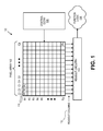
- FIG. 1 is a diagram that shows generally one example of an HDR imaging system 100 including an example pixel array 102 having pixels that include at least a short integration photodiode and a long integration photodiode in accordance with the teachings of the present invention.
- the short integration photodiode of each pixel has a smaller light exposure area and a higher overall doping concentration compared to the long integration photodiode of the pixel.
- the short integration photodiode and the long integration photodiode are realized using a single implantation step in accordance with the teachings of the present invention.
- HDR imaging system 100 includes pixel array 102 coupled to control circuitry 108 and readout circuitry 104, which is coupled to function logic 106.
- pixel array 102 is a two-dimensional (2D) array of imaging sensors or pixels 110 (e.g., pixels P1, P2 ..., Pn).
- each pixel 110 is a CMOS imaging pixel including at least a short integration photodiode and a long integration photodiode.
- short integration photodiode of each pixel 110 has a smaller light exposure area and a higher overall doping concentration compared to the long integration photodiode of the pixel 110.
- each pixel 110 is arranged into a row (e.g., rows R1 to Ry) and a column (e.g., column C1 to Cx) to acquire image data of a person, place, object, etc., which can then be used to render an image of the person, place, object, etc.
- a row e.g., rows R1 to Ry
- a column e.g., column C1 to Cx
- readout circuitry 104 may include amplification circuitry, analog-to-digital (ADC) conversion circuitry, or otherwise.
- Function logic 106 may simply store the image data or even manipulate the image data by applying post image effects (e.g., crop, rotate, remove red eye, adjust brightness, adjust contrast, or otherwise).
- readout circuitry 104 may read out a row of image data at a time along readout column lines (illustrated) or may read out the image data using a variety of other techniques (not illustrated), such as a serial read out or a full parallel read out of all pixels simultaneously.
- control circuitry 108 is coupled to pixel array 102 to control operational characteristics of pixel array 102.
- control circuitry 108 may generate a shutter signal for controlling image acquisition.
- the shutter signal is a global shutter signal for simultaneously enabling all pixels within pixel array 102 to simultaneously capture their respective image data during a single acquisition window.
- the shutter signal is a rolling shutter signal such that each row, column, or group of pixels is sequentially enabled during consecutive acquisition windows.
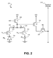
- FIG. 2 is a schematic illustrating one example of a pixel 210 in accordance with the teachings of the present invention.
- pixel 210 may be one of the plurality of pixels 110 included in the example pixel array 102 of the HDR image sensor 100 illustrated above in FIG. 1 .
- pixel 210 includes a short integration photodiode PD S 216 and a long integration photodiode PD L 214.
- long integration photodiode PD L 214 has a larger light exposure area than the light exposure area of short integration photodiode PD S 216.
- long integration photodiode PD L 214 has higher sensitivity to incident light and is therefore utilized for lower light intensity sensing.
- short integration photodiode PD S 216 on the other hand has less light exposure area, it is less sensitive to light compared to long integration photodiode PD L 214, and is therefore utilized for higher light intensity sensing.
- charge that is accumulated in long integration photodiode PD L 214 is switched through transfer transistor T1 L 218 to a floating drain FD L 228 in response to a control signal TX L and charge that is accumulated in short integration photodiode PD S 216 is switched through transfer transistor T1 S 2220 to a floating drain FD S 229 in response to a control signal TX S .
- the floating drains FD L 228 and FD S 229 are each physically located near their respective transfer transistors T1 L 218 and T1 S 220.
- pixel 210 also includes an amplifier transistor T3 224 that has a gate terminal coupled to floating drain FD L 228 and floating drain FD S 229.
- amplifier transistor T3 224 is coupled in a source follower configuration as shown, which therefore amplifies an input signal at the gate terminal of amplifier transistor T3 224 to an output signal at the source terminal of amplifier transistor T3 224.
- row select transistor T4 226 is coupled to the source terminal of amplifier transistor T3 224 to selectively switch the output of amplifier transistor T3 231 to readout column 212 in response to a control signal SEL.
- pixel 210 also includes reset transistor 241 coupled to floating drain FD 228, long integration photodiode PD L 214 and short integration photodiode PD S 216, which may be used to reset charge accumulated in pixel 210 in response to a reset signal RST.
- the charge accumulated in floating drain FD 228, long integration photodiode PD L 214 and short integration photodiode PD S 216 can be reset during an initialization period of pixel 210, or for example each time after charge information has been read out from pixel 210 and prior to accumulating charge in long integration photodiode PD L 214 and short integration photodiode PD S 216 for the acquisition of a new HDR image in accordance with the teachings of the present invention.
- long integration photodiode PD L 214 and short integration photodiode PD S 216 are designed to have either photodiode appear to have the same electrical characteristics to amplifier transistor T3 224 for improved performance of pixel 210.
- Separate implantation steps are typically performed to individually tailor the electrical characteristics of long integration photodiode PD L 214 and short integration photodiode PD S 216 to compensate for the substantial difference in light exposure areas between long integration photodiode PD L 214 and short integration photodiode PD S 216.
- FIG. 3A shows a top down view of a portion of a pixel 310A included a pixel array 302A.
- pixel 310A includes a long integration photodiode 314A and short integration photodiode 316A disposed in semiconductor material 330A.
- the light exposure area of long integration photodiode 314A is substantially larger than the light exposure area of short integration photodiode 316A.
- long integration photodiode 314A has higher light sensitivity for lower light intensity sensing and short integration photodiode 316A has lower light sensitivity for higher light intensity sensing.
- the doping concentration of long integration photodiode 314A is less than the doping concentration of short integration photodiode 316A.
- the full well charge capacities of long integration photodiode 314A and short integration photodiode 316A are comparable to compensate for the substantial difference in area between long integration photodiode 314A and short integration photodiode 316A.
- the dopants are implanted for short integration photodiode 316A and long integration photodiode 314A in separate implantation steps for pixel 310A. That is, the dopants for long integration photodiode 314A are implanted using a separate and lower implant dose (e.g., shown as "Dose 1" in FIG. 3A ) compared to a higher implant dose (e.g., shown as "Dose 2" in FIG. 3A ) in short integration photodiode 316A.
- a separate and lower implant dose e.g., shown as "Dose 1" in FIG. 3A
- a higher implant dose e.g., shown as "Dose 2" in FIG. 3A
- the resulting implant dose for one example of short integration photodiode 316A is in a range between 4x10 12 cm -2 and 6x10 12 cm -2 and the resulting implant dose for one example of long integration photodiode 314A is in a range between 2x10 12 cm -2 and 4x10 12 cm -2 .
- FIG. 3B shows a top down view of a portion of a pixel 310B in a pixel array 302B in accordance with the teachings of the present invention.
- pixel 310B includes a long integration photodiode 314B and short integration photodiode 316B disposed in semiconductor material 330B.
- the light exposure area of long integration photodiode 314A is substantially larger than the light exposure area of short integration photodiode 316A.
- long integration photodiode 314A has higher light sensitivity for lower light intensity sensing and short integration photodiode 316A has lower light sensitivity for higher light intensity sensing.
- pixel 310B may be pixel 210 of FIG. 2 , or one of the plurality of pixels 110 included in the example pixel array 102 of the HDR image sensor 100 illustrated above in FIG. 1 .
- the light exposure area of long integration photodiode 314B is substantially larger than the light exposure area of short integration photodiode 316B such that long integration photodiode 314B has higher light sensitivity for lower light intensity sensing and short integration photodiode 316B has lower light sensitivity for higher light intensity sensing in accordance with the teachings of the present invention.
- the light exposure area of long integration photodiode 314B is shaped to include at least one implanted portion 332 and at least one non-implanted portion 334 in accordance with the teachings of the present invention.
- the at least one implanted portion 332 of long integration photodiode 314B is implanted with dopants during the same single implantation step in which the short integration photodiode 316B is implanted with dopants (e.g., "Dose 1" as illustrated in FIG. 3B ) in accordance with the teachings of the present invention.
- the implant dose of short integration photodiode 316B as well as the implant dose of the at least one implanted portion 332 of long integration photodiode 314B are both in a range between 4x10 12 cm -2 and 6x10 12 cm -2 .
- long integration photodiode 314B also includes at least one non-implanted portion 334, which was shielded from being implanted with dopants during the single implantation step in which the short integration photodiode 316B and implanted portion 332 were implanted with dopants (e.g., "Dose 1")
- the combined doping concentration of the at least one implanted portion 332 and the at least one non-implanted portion 334 of the long integration photodiode 314B is less than the doping concentration of short integration photodiode 316B.
- the combined doping concentration of implanted portion 332 and non-implanted portion 334 of long integration photodiode 314B in FIG. 3B is in a range between 2x10 16 cm -3 and 4x10 16 cm -3 .
- the full well charge capacity of the short integration photodiode 316B is substantially equal to the full well charge capacity of the long integration photodiode 314B, even though the area of the long integration photodiode 314B is substantially larger than the area of short integration photodiode 316B in accordance with the teachings of the present invention.
- the at least one non-implanted portion 334 of long integration photodiode 314B is small enough such that the at least one non-implanted portion 334 remains depleted of charge carriers during image acquisition. That is, the larger long integration photodiode 314B still acts like a larger area photodetector with corresponding higher sensitivity to low light, while the full well charge capacity and charge gain of long integration photodiode 314B appear to the amplifier (e.g. amplifier transistor T3 224 of FIG. 2 ) to be more like the smaller short integration photodiode 316B in accordance with the teachings of the present invention.
- the amplifier e.g. amplifier transistor T3 224 of FIG. 2
- implant dose ranges of between 4x10 12 cm -2 and 6x10 12 cm -2 and between 2x10 12 cm -2 and 4x10 12 cm -2 are provided above for explanation purposes and that other implant doses may be utilized to realize pixel 310B in accordance with he the teachings of the present invention.
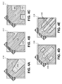
- FIGs. 4A-4E illustrate various possible examples of long integration photodiodes 414A, 414B, 414C, 414D and 414E, respectively, which may be included in an example HDR pixel having at least one implanted portion and at least one non-implanted portion in accordance with the teachings of the present invention. It is appreciated that any of the long integration photodiodes 414A, 414B, 414C, 414D and 414E as shown in FIGs. 4A-4E , respectively, may be used in place of example long integration photodiode 314B of FIG. 3 B.
- the at least one implanted portion 432A of long integration photodiode 414A is photomasked and implanted with dopants at the same time in which the corresponding short integration photodiode (e.g., short integration photodiode 316B of FIG. 3B ) is photomasked and implanted with dopants.
- the photomask used to form the at least one implanted portion 432A results in at least one non-implanted portion 434A in long integration photodiode 414A as shown.
- FIG. 4A the example depicted in FIG.
- the at least one non-implanted portion 434A extends from one corner towards an opposite corner of long integration photodiode 414A as shown. Since the at least one non-implanted portion 434A is shielded from being implanted with dopants while the at least one implanted portion 432A is implanted with dopants, the doping concentration of the at least one non-implanted portion 434A is less than the doping concentration of the at least one implanted portion 432A. Therefore, the combined doping concentration of the at least one implanted portion 432A and the at least one non-implanted portion 434A is less than the doping concentration of the at least one implanted portion 432A in accordance with the teachings of the present invention.
- the at least one implanted portion 432B of long integration photodiode 414B is photomasked and implanted with dopants at the same time in which the corresponding short integration photodiode (e.g., short integration photodiode 316B of FIG. 3B ) is photomasked and implanted with dopants.
- the photomask used to form the at least one implanted portion 432B results in non-implanted portions 434B in long integration photodiode 414B as shown.
- FIG. 4B the example depicted in FIG.
- the non-implanted portions 434B extend from two adjacent sides of long integration photodiode 414B towards respective opposite sides of long integration photodiode 414B as shown. Since the non-implanted portions 434B are shielded from being implanted with dopants while the at least one implanted portion 432B is implanted with dopants, the doping concentration of the non-implanted portions 434B is less than the doping concentration of the at least one implanted portion 432B. Therefore, the combined doping concentration of the at least one implanted portion 432B and the non-implanted portions 434B is less than the doping concentration of the at least one implanted portion 432B in accordance with the teachings of the present invention.
- the at least one implanted portion 432C of long integration photodiode 414C is photomasked and implanted with dopants at the same time in which the corresponding short integration photodiode (e.g., short integration photodiode 316B of FIG. 3B ) is photomasked and implanted with dopants.
- the photomask used to form the at least one implanted portion 432C results in non-implanted portions 434C in long integration photodiode 414C as shown.
- FIG. 4C the example depicted in FIG.
- the non-implanted portions 434C extend from a corner and two sides of long integration photodiode 414C towards the center of long integration photodiode 414C as shown. Since the non-implanted portions 434C are shielded from being implanted with dopants while the at least one implanted portion 432C is implanted with dopants, the doping concentration of the non-implanted portions 434C is less than the doping concentration of the at least one implanted portion 432C. Therefore, the combined doping concentration of the at least one implanted portion 432C and the non-implanted portions 434C is less than the doping concentration of the at least one implanted portion 432C in accordance with the teachings of the present invention.
- the at least one implanted portion 432D of long integration photodiode 414D is photomasked and implanted with dopants at the same time in which the corresponding short integration photodiode (e.g., short integration photodiode 316B of FIG. 3B ) is photomasked and implanted with dopants.
- the photomask used to form the at least one implanted portion 432D results in non-implanted portions 434D in long integration photodiode 414D as shown.
- FIG. 4D the example depicted in FIG.
- the non-implanted portions 434D include a plurality of regions enclosed entirely within the at least one implanted portion 432D of long integration photodiode 414D as shown. Since the non-implanted portions 434D are shielded from being implanted with dopants while the at least one implanted portion 432D is implanted with dopants, the doping concentration of the non-implanted portions 434D is less than the doping concentration of the at least one implanted portion 432D. Therefore, the combined doping concentration of the at least one implanted portion 432D and the non-implanted portions 434D is less than the doping concentration of the at least one implanted portion 432D in accordance with the teachings of the present invention.
- the at least one implanted portion 432E of long integration photodiode 414E is photomasked and implanted with dopants at the same time in which the corresponding short integration photodiode (e.g., short integration photodiode 316B of FIG. 3B ) is photomasked and implanted with dopants.
- the photomask used to form the at least one implanted portion 432E results in non-implanted portions 434E in long integration photodiode 414E as shown.
- FIG. 4E the example depicted in FIG.
- the non-implanted portions 434E include a plurality of regions that extend from one corner towards an opposite corner of long integration photodiode 414E as shown. Since the non-implanted portions 434E are shielded from being implanted with dopants while the at least one implanted portion 432E is implanted with dopants, the doping concentration of the non-implanted portions 434E is less than the doping concentration of the at least one implanted portion 432E. Therefore, the combined doping concentration of the at least one implanted portion 432E and the non-implanted portions 434E is less than the doping concentration of the at least one implanted portion 432E in accordance with the teachings of the present invention.
- FIGs. 4A-4E are provided for explanation purposes and that other shapes for the implanted and non-implanted portions in a long integration photodiode may be utilized in accordance with the teachings of the present invention.
Landscapes
- Solid State Image Pick-Up Elements (AREA)
- Transforming Light Signals Into Electric Signals (AREA)
Abstract
A high dynamic range image sensor pixel includes a short integration photodiode and a long integration photodiode disposed in semiconductor material. The long integration photodiode has a light exposure area that is substantially larger than a light exposure area of the short integration photodiode. The light exposure area of the short integration photodiode has a first doping concentration from a first doping implantation. The light exposure area of the long integration photodiode includes at least one implanted portion having the first doping concentration from the first doping implantation. The light exposure area of the long integration photodiode further includes at least one non-implanted portion photomasked from the first doping implantation such that a combined doping concentration of the implanted and non-implanted portions of the light exposure area of the long integration photodiode is less than the first doping concentration of the light exposure area of the short integration photodiode.
Description
- The present invention is generally related to high dynamic range image sensors, and more specifically, the present invention is directed to high dynamic range image sensors having a plurality of photodiodes in each pixel.
- High dynamic range (HDR) image sensors are useful for many applications. In general, ordinary image sensors, including for example charge coupled device (CCD) and complementary metal oxide semiconductor (CMOS) image sensors, have a dynamic range of approximately 70 dB dynamic range. In comparison, the human eye has a dynamic range of up to approximately 100 dB. There are a variety of situation in which an image sensor having an increased dynamic range is beneficial. For example, image sensors having a dynamic range of more than 100 dB dynamic range are needed in the automotive industry are necessary in order to handle different driving conditions, such as driving from a dark tunnel into bright sunlight. Indeed, many applications may require image sensors with at least 90 dB of dynamic range or more to accommodate a wide range of lighting situations, varying from low light conditions to bright light conditions.
- One known approach for implementing HDR image sensors is to use a combination of a photodiodes in each pixel. One of the photodiodes can be used to sense bright light conditions while another photodiode can be used to sense low light conditions. However, one challenge with manufacturing HDR image sensors using this approach is that additional photo masking and implantation steps are required during manufacture, which add to the overall complexity and cost of implementing the HDR image sensors. Furthermore, the additional photomasking and implantation steps result in lower yields of HDR image sensors that are manufactured using this approach.
- Non-limiting and non-exhaustive embodiments of the present invention are described with reference to the following figures, wherein like reference numerals refer to like parts throughout the various views unless otherwise specified.
-
FIG. 1 is a diagram illustrating one example of an imaging system including an example HDR image sensor in accordance with the teachings of the present invention. -
FIG. 2 is a schematic illustrating one example of an HDR pixel including a plurality of photodiodes in accordance with the teachings of the present invention. -
FIG. 3A illustrates a top down view of one example of an HDR pixel included in an example pixel array having multiple implantations. -
FIG. 3B illustrates a top down view of one example of an HDR pixel included in an example pixel array having a single implantation in accordance with the teachings of the present invention. -
FIGs. 4A-4E illustrate various other examples of a long integration photodiodes included in example HDR pixels having at least one implanted portion and at least one non-implanted portion in accordance with the teachings of the present invention. - Corresponding reference characters indicate corresponding components throughout the several views of the drawings. Skilled artisans will appreciate that elements in the figures are illustrated for simplicity and clarity and have not necessarily been drawn to scale. For example, the dimensions of some of the elements in the figures may be exaggerated relative to other elements to help to improve understanding of various embodiments of the present invention. Also, common but well-understood elements that are useful or necessary in a commercially feasible embodiment are often not depicted in order to facilitate a less obstructed view of these various embodiments of the present invention.
- In the following description, numerous specific details are set forth in order to provide a thorough understanding of the present invention. It will be apparent, however, to one having ordinary skill in the art that the specific detail need not be employed to practice the present invention. In other instances, well-known materials or methods have not been described in detail in order to avoid obscuring the present invention.
- Reference throughout this specification to "one embodiment", "an embodiment", "one example" or "an example" means that a particular feature, structure or characteristic described in connection with the embodiment or example is included in at least one embodiment of the present invention. Thus, appearances of the phrases "in one embodiment", "in an embodiment", "one example" or "an example" in various places throughout this specification are not necessarily all referring to the same embodiment or example. Furthermore, the particular features, structures or characteristics may be combined in any suitable combinations and/or subcombinations in one or more embodiments or examples. Particular features, structures or characteristics may be included in an integrated circuit, an electronic circuit, a combinational logic circuit, or other suitable components that provide the described functionality. In addition, it is appreciated that the figures provided herewith are for explanation purposes to persons ordinarily skilled in the art and that the drawings are not necessarily drawn to scale.
- Examples in accordance with the teaching of the present invention describe an image sensor pixel for use in a high dynamic range (HDR) image sensor, including at least a short integration photodiode and a long integration photodiode. In various examples, the short integration photodiode has a smaller light exposure area and a higher overall doping concentration compared to the long integration photodiode of the pixel. As will be described, examples of the short integration photodiode and a long integration photodiode are realized using a single implantation step in accordance with the teachings of the present invention. Since separate implantation steps and associated photomasking steps for the short integration photodiode and a long integration photodiode are combined, the overall complexity and cost of manufacturing an HDR image sensor is reduced accordance with the teachings of the present invention. Furthermore, the reduced of the number of photomasking and implantation steps required for manufacture also results in increased yields of HDR image sensors in accordance with the teachings of the present invention.
- To illustrate,
FIG. 1 is a diagram that shows generally one example of anHDR imaging system 100 including anexample pixel array 102 having pixels that include at least a short integration photodiode and a long integration photodiode in accordance with the teachings of the present invention. In the example, the short integration photodiode of each pixel has a smaller light exposure area and a higher overall doping concentration compared to the long integration photodiode of the pixel. In the depicted example, the short integration photodiode and the long integration photodiode are realized using a single implantation step in accordance with the teachings of the present invention. As shown in the depicted example,HDR imaging system 100 includespixel array 102 coupled tocontrol circuitry 108 andreadout circuitry 104, which is coupled tofunction logic 106. - In one example,
pixel array 102 is a two-dimensional (2D) array of imaging sensors or pixels 110 (e.g., pixels P1, P2 ..., Pn). In one example, eachpixel 110 is a CMOS imaging pixel including at least a short integration photodiode and a long integration photodiode. In the depicted example, short integration photodiode of eachpixel 110 has a smaller light exposure area and a higher overall doping concentration compared to the long integration photodiode of thepixel 110. As illustrated, eachpixel 110 is arranged into a row (e.g., rows R1 to Ry) and a column (e.g., column C1 to Cx) to acquire image data of a person, place, object, etc., which can then be used to render an image of the person, place, object, etc. - In one example, after each
pixel 110 has acquired its image data or image charge, the image data is read out byreadout circuitry 104 throughreadout columns 112 and then transferred tofunction logic 106. In various examples,readout circuitry 104 may include amplification circuitry, analog-to-digital (ADC) conversion circuitry, or otherwise.Function logic 106 may simply store the image data or even manipulate the image data by applying post image effects (e.g., crop, rotate, remove red eye, adjust brightness, adjust contrast, or otherwise). In one example,readout circuitry 104 may read out a row of image data at a time along readout column lines (illustrated) or may read out the image data using a variety of other techniques (not illustrated), such as a serial read out or a full parallel read out of all pixels simultaneously. - In one example,
control circuitry 108 is coupled topixel array 102 to control operational characteristics ofpixel array 102. For example,control circuitry 108 may generate a shutter signal for controlling image acquisition. In one example, the shutter signal is a global shutter signal for simultaneously enabling all pixels withinpixel array 102 to simultaneously capture their respective image data during a single acquisition window. In another example, the shutter signal is a rolling shutter signal such that each row, column, or group of pixels is sequentially enabled during consecutive acquisition windows. -
FIG. 2 is a schematic illustrating one example of apixel 210 in accordance with the teachings of the present invention. In one example, it is appreciated thatpixel 210 may be one of the plurality ofpixels 110 included in theexample pixel array 102 of theHDR image sensor 100 illustrated above inFIG. 1 . As shown in the example depicted inFIG. 2 ,pixel 210 includes a shortintegration photodiode PD S 216 and a longintegration photodiode PD L 214. As will be discussed in further detail below, longintegration photodiode PD L 214 has a larger light exposure area than the light exposure area of shortintegration photodiode PD S 216. Thus, longintegration photodiode PD L 214 has higher sensitivity to incident light and is therefore utilized for lower light intensity sensing. Since shortintegration photodiode PD S 216 on the other hand has less light exposure area, it is less sensitive to light compared to longintegration photodiode PD L 214, and is therefore utilized for higher light intensity sensing. By utilizing both longintegration photodiode PD L 214 and shortintegration photodiode PD S 216 inpixel 210, HDR imaging sensing is realized in accordance with the teaching of the present invention. - Continuing with example depicted in
FIG. 2 , charge that is accumulated in longintegration photodiode PD L 214 is switched throughtransfer transistor T1 L 218 to a floatingdrain FD L 228 in response to a control signal TXL and charge that is accumulated in shortintegration photodiode PD S 216 is switched through transfer transistor T1S 2220 to a floatingdrain FD S 229 in response to a control signal TXS. In one example, the floating drains FDL 228 andFD S 229 are each physically located near their respectivetransfer transistors T1 L 218 andT1 S 220. - As shown in the example,
pixel 210 also includes anamplifier transistor T3 224 that has a gate terminal coupled to floatingdrain FD L 228 and floatingdrain FD S 229. Thus, in the illustrated example, the charge from longintegration photodiode PD L 214 and shortintegration photodiode PD S 216 are separately switched to floatingdrain FD L 228 and floatingdrain FD S 229, respectively, which share the sameamplifier transistor T3 224. In one example,amplifier transistor T3 224 is coupled in a source follower configuration as shown, which therefore amplifies an input signal at the gate terminal ofamplifier transistor T3 224 to an output signal at the source terminal ofamplifier transistor T3 224. As shown, rowselect transistor T4 226 is coupled to the source terminal ofamplifier transistor T3 224 to selectively switch the output of amplifier transistor T3 231 toreadout column 212 in response to a control signal SEL. As shown in the example,pixel 210 also includes reset transistor 241 coupled to floatingdrain FD 228, longintegration photodiode PD L 214 and shortintegration photodiode PD S 216, which may be used to reset charge accumulated inpixel 210 in response to a reset signal RST. In one example, the charge accumulated in floatingdrain FD 228, longintegration photodiode PD L 214 and shortintegration photodiode PD S 216 can be reset during an initialization period ofpixel 210, or for example each time after charge information has been read out frompixel 210 and prior to accumulating charge in longintegration photodiode PD L 214 and shortintegration photodiode PD S 216 for the acquisition of a new HDR image in accordance with the teachings of the present invention. - In one example, long
integration photodiode PD L 214 and shortintegration photodiode PD S 216 are designed to have either photodiode appear to have the same electrical characteristics toamplifier transistor T3 224 for improved performance ofpixel 210. Separate implantation steps are typically performed to individually tailor the electrical characteristics of longintegration photodiode PD L 214 and shortintegration photodiode PD S 216 to compensate for the substantial difference in light exposure areas between longintegration photodiode PD L 214 and shortintegration photodiode PD S 216. - To illustrate,
FIG. 3A shows a top down view of a portion of apixel 310A included apixel array 302A. In the example,pixel 310A includes along integration photodiode 314A andshort integration photodiode 316A disposed insemiconductor material 330A. As shown in the depicted example, the light exposure area oflong integration photodiode 314A is substantially larger than the light exposure area ofshort integration photodiode 316A. As a result,long integration photodiode 314A has higher light sensitivity for lower light intensity sensing andshort integration photodiode 316A has lower light sensitivity for higher light intensity sensing. - In order for
long integration photodiode 314A andshort integration photodiode 316A to have the same electrical characteristics with respect to the corresponding amplifier transistor (e.g.,amplifier transistor T3 224 ofFIG. 2 ), the doping concentration oflong integration photodiode 314A is less than the doping concentration ofshort integration photodiode 316A. As such, the full well charge capacities oflong integration photodiode 314A andshort integration photodiode 316A are comparable to compensate for the substantial difference in area betweenlong integration photodiode 314A andshort integration photodiode 316A. - In order to realize the different doping concentrations for
long integration photodiode 314A andshort integration photodiode 316A, the dopants are implanted forshort integration photodiode 316A andlong integration photodiode 314A in separate implantation steps forpixel 310A. That is, the dopants forlong integration photodiode 314A are implanted using a separate and lower implant dose (e.g., shown as "Dose 1" inFIG. 3A ) compared to a higher implant dose (e.g., shown as "Dose 2" inFIG. 3A ) inshort integration photodiode 316A. Consequently, there are also separate photomasking steps corresponding to the separate implantation (e.g., "Dose 1" and "Dose 2") forlong integration photodiode 314A andshort integration photodiode 316A. Using the separate photomasking and implantation steps as described forlong integration photodiode 314A andshort integration photodiode 316A as illustrated inFIG. 3A , the resulting implant dose for one example ofshort integration photodiode 316A is in a range between 4x1012 cm-2 and 6x1012 cm-2 and the resulting implant dose for one example oflong integration photodiode 314A is in a range between 2x1012 cm-2 and 4x1012 cm-2. It is appreciated that with the separate photomasking and implantation steps performed to realizelong integration photodiode 314A andshort integration photodiode 316A, the overall complexity and cost to manufacturepixel 310A is increased with each additional step. Furthermore, the additional photomasking and implantation steps result in lower yields forpixel 310A. -
FIG. 3B shows a top down view of a portion of apixel 310B in apixel array 302B in accordance with the teachings of the present invention. In the example,pixel 310B includes along integration photodiode 314B andshort integration photodiode 316B disposed insemiconductor material 330B. As shown in the depicted example, the light exposure area oflong integration photodiode 314A is substantially larger than the light exposure area ofshort integration photodiode 316A. As a result,long integration photodiode 314A has higher light sensitivity for lower light intensity sensing andshort integration photodiode 316A has lower light sensitivity for higher light intensity sensing. In one example, it is appreciated thatpixel 310B may bepixel 210 ofFIG. 2 , or one of the plurality ofpixels 110 included in theexample pixel array 102 of theHDR image sensor 100 illustrated above inFIG. 1 . As shown in the example depicted inFIG. 3B , the light exposure area oflong integration photodiode 314B is substantially larger than the light exposure area ofshort integration photodiode 316B such thatlong integration photodiode 314B has higher light sensitivity for lower light intensity sensing andshort integration photodiode 316B has lower light sensitivity for higher light intensity sensing in accordance with the teachings of the present invention. - As illustrated the depicted example, the light exposure area of
long integration photodiode 314B is shaped to include at least one implantedportion 332 and at least onenon-implanted portion 334 in accordance with the teachings of the present invention. In the depicted example, the at least one implantedportion 332 oflong integration photodiode 314B is implanted with dopants during the same single implantation step in which theshort integration photodiode 316B is implanted with dopants (e.g., "Dose 1" as illustrated inFIG. 3B ) in accordance with the teachings of the present invention. Accordingly, in one example, the implant dose ofshort integration photodiode 316B as well as the implant dose of the at least one implantedportion 332 oflong integration photodiode 314B are both in a range between 4x1012 cm-2 and 6x1012 cm-2. - However, since
long integration photodiode 314B also includes at least onenon-implanted portion 334, which was shielded from being implanted with dopants during the single implantation step in which theshort integration photodiode 316B and implantedportion 332 were implanted with dopants (e.g., "Dose 1"), the combined doping concentration of the at least one implantedportion 332 and the at least onenon-implanted portion 334 of thelong integration photodiode 314B is less than the doping concentration ofshort integration photodiode 316B. In one example, where the mean implant depth is about one micrometer, the combined doping concentration of implantedportion 332 andnon-implanted portion 334 oflong integration photodiode 314B inFIG. 3B is in a range between 2x1016 cm-3 and 4x1016 cm-3. Thus, in the illustrated example, the full well charge capacity of theshort integration photodiode 316B is substantially equal to the full well charge capacity of thelong integration photodiode 314B, even though the area of thelong integration photodiode 314B is substantially larger than the area ofshort integration photodiode 316B in accordance with the teachings of the present invention. - During operation, the at least one
non-implanted portion 334 oflong integration photodiode 314B is small enough such that the at least onenon-implanted portion 334 remains depleted of charge carriers during image acquisition. That is, the largerlong integration photodiode 314B still acts like a larger area photodetector with corresponding higher sensitivity to low light, while the full well charge capacity and charge gain oflong integration photodiode 314B appear to the amplifier (e.g.amplifier transistor T3 224 ofFIG. 2 ) to be more like the smallershort integration photodiode 316B in accordance with the teachings of the present invention. - Therefore, it is appreciated that since both
short integration photodiode 316B and the at least one implantedportion 332 oflong integration photodiode 314B are photomasked and implanted using the same combined photomasking and implantation steps, the overall number of steps to manufacturepixel 310B is reduced since separate photomasking and implantation steps are no longer needed to form short integration photodiode 316 andlong integration photodiode 314B in accordance with the teachings of the present invention. As a result, the overall complexity and cost to manufacturepixel 310B is reduced. Furthermore, with fewer photomasking and implantation steps needed in order to manufacturepixel 310B, increased yields may be realized forpixel 310B in accordance with the teachings of the present invention. - It is appreciated that the examples of implant dose ranges of between 4x1012 cm-2 and 6x1012 cm-2 and between 2x1012 cm-2 and 4x1012 cm-2 are provided above for explanation purposes and that other implant doses may be utilized to realize
pixel 310B in accordance with he the teachings of the present invention. -
FIGs. 4A-4E illustrate various possible examples oflong integration photodiodes long integration photodiodes FIGs. 4A-4E , respectively, may be used in place of examplelong integration photodiode 314B ofFIG. 3 B. - In the example depicted in
FIG. 4A , the at least one implantedportion 432A oflong integration photodiode 414A is photomasked and implanted with dopants at the same time in which the corresponding short integration photodiode (e.g.,short integration photodiode 316B ofFIG. 3B ) is photomasked and implanted with dopants. As shown in the example, the photomask used to form the at least one implantedportion 432A results in at least one non-implanted portion 434A inlong integration photodiode 414A as shown. In the example depicted inFIG. 4A , the at least one non-implanted portion 434A extends from one corner towards an opposite corner oflong integration photodiode 414A as shown. Since the at least one non-implanted portion 434A is shielded from being implanted with dopants while the at least one implantedportion 432A is implanted with dopants, the doping concentration of the at least one non-implanted portion 434A is less than the doping concentration of the at least one implantedportion 432A. Therefore, the combined doping concentration of the at least one implantedportion 432A and the at least one non-implanted portion 434A is less than the doping concentration of the at least one implantedportion 432A in accordance with the teachings of the present invention. - Similarly, as shown the example depicted in
FIG. 4B , the at least one implantedportion 432B oflong integration photodiode 414B is photomasked and implanted with dopants at the same time in which the corresponding short integration photodiode (e.g.,short integration photodiode 316B ofFIG. 3B ) is photomasked and implanted with dopants. As shown in the example, the photomask used to form the at least one implantedportion 432B results innon-implanted portions 434B inlong integration photodiode 414B as shown. In the example depicted inFIG. 4B , thenon-implanted portions 434B extend from two adjacent sides oflong integration photodiode 414B towards respective opposite sides oflong integration photodiode 414B as shown. Since thenon-implanted portions 434B are shielded from being implanted with dopants while the at least one implantedportion 432B is implanted with dopants, the doping concentration of thenon-implanted portions 434B is less than the doping concentration of the at least one implantedportion 432B. Therefore, the combined doping concentration of the at least one implantedportion 432B and thenon-implanted portions 434B is less than the doping concentration of the at least one implantedportion 432B in accordance with the teachings of the present invention. - Similarly, as shown the example depicted in
FIG. 4C , the at least one implantedportion 432C oflong integration photodiode 414C is photomasked and implanted with dopants at the same time in which the corresponding short integration photodiode (e.g.,short integration photodiode 316B ofFIG. 3B ) is photomasked and implanted with dopants. As shown in the example, the photomask used to form the at least one implantedportion 432C results innon-implanted portions 434C inlong integration photodiode 414C as shown. In the example depicted inFIG. 4C , thenon-implanted portions 434C extend from a corner and two sides oflong integration photodiode 414C towards the center oflong integration photodiode 414C as shown. Since thenon-implanted portions 434C are shielded from being implanted with dopants while the at least one implantedportion 432C is implanted with dopants, the doping concentration of thenon-implanted portions 434C is less than the doping concentration of the at least one implantedportion 432C. Therefore, the combined doping concentration of the at least one implantedportion 432C and thenon-implanted portions 434C is less than the doping concentration of the at least one implantedportion 432C in accordance with the teachings of the present invention. - Similarly, as shown the example depicted in
FIG. 4D , the at least one implantedportion 432D oflong integration photodiode 414D is photomasked and implanted with dopants at the same time in which the corresponding short integration photodiode (e.g.,short integration photodiode 316B ofFIG. 3B ) is photomasked and implanted with dopants. As shown in the example, the photomask used to form the at least one implantedportion 432D results innon-implanted portions 434D inlong integration photodiode 414D as shown. In the example depicted inFIG. 4D , thenon-implanted portions 434D include a plurality of regions enclosed entirely within the at least one implantedportion 432D oflong integration photodiode 414D as shown. Since thenon-implanted portions 434D are shielded from being implanted with dopants while the at least one implantedportion 432D is implanted with dopants, the doping concentration of thenon-implanted portions 434D is less than the doping concentration of the at least one implantedportion 432D. Therefore, the combined doping concentration of the at least one implantedportion 432D and thenon-implanted portions 434D is less than the doping concentration of the at least one implantedportion 432D in accordance with the teachings of the present invention. - Similarly, as shown the example depicted in
FIG. 4E , the at least one implantedportion 432E oflong integration photodiode 414E is photomasked and implanted with dopants at the same time in which the corresponding short integration photodiode (e.g.,short integration photodiode 316B ofFIG. 3B ) is photomasked and implanted with dopants. As shown in the example, the photomask used to form the at least one implantedportion 432E results innon-implanted portions 434E inlong integration photodiode 414E as shown. In the example depicted inFIG. 4E , thenon-implanted portions 434E include a plurality of regions that extend from one corner towards an opposite corner oflong integration photodiode 414E as shown. Since thenon-implanted portions 434E are shielded from being implanted with dopants while the at least one implantedportion 432E is implanted with dopants, the doping concentration of thenon-implanted portions 434E is less than the doping concentration of the at least one implantedportion 432E. Therefore, the combined doping concentration of the at least one implantedportion 432E and thenon-implanted portions 434E is less than the doping concentration of the at least one implantedportion 432E in accordance with the teachings of the present invention. - It is appreciated that the examples depicted in
FIGs. 4A-4E are provided for explanation purposes and that other shapes for the implanted and non-implanted portions in a long integration photodiode may be utilized in accordance with the teachings of the present invention. - The above description of illustrated examples of the present invention, including what is described in the Abstract, are not intended to be exhaustive or to be limitation to the precise forms disclosed. While specific embodiments of, and examples for, the invention are described herein for illustrative purposes, various equivalent modifications are possible without departing from the broader spirit and scope of the present invention.
- These modifications can be made to examples of the invention in light of the above detailed description. The terms used in the following claims should not be construed to limit the invention to the specific embodiments disclosed in the specification and the claims. Rather, the scope is to be determined entirely by the following claims, which are to be construed in accordance with established doctrines of claim interpretation. The present specification and figures are accordingly to be regarded as illustrative rather than restrictive.
Claims (10)
- An image sensor pixel for use in a high dynamic range image sensor, comprising:a short integration photodiode disposed in semiconductor material, the short integration photodiode having a first light exposure area, wherein the first light exposure area has a first doping concentration from a first doping implantation; anda long integration photodiode disposed in the semiconductor material, the long integration photodiode having a second light exposure area, wherein the second light exposure area is substantially larger than the first light exposure area, wherein the second light exposure area includes at least one implanted portion having the first doping concentration from the first doping implantation, wherein the second light exposure area further includes at least one non-implanted portion photomasked from the first doping implantation such that a combined doping concentration of the implanted and non-implanted portions of the second light exposure area is less than the first doping concentration of the first light exposure area.
- The image sensor pixel of claim 1 wherein a charge capacity of the short integration photodiode is substantially equal to a charge capacity of the long integration photodiode.
- The image sensor pixel of claim 1 wherein the long integration photodiode has greater sensitivity to light than the short integration diode.
- The image sensor pixel of claim 1 wherein the at least one non-implanted portion of the second light exposure area remains substantially depleted of charge carriers during image collection.
- The image sensor pixel of claim 1 further comprising first and second floating drains disposed in the semiconductor material coupled to the short integration photodiode and the long integration photodiode through first and second transfer transistors, respectively, wherein the first and second transfer transistors are separately switched.
- The image sensor pixel of claim 5 further comprising a reset transistor disposed in the semiconductor material coupled to the first and second floating drains.
- The image sensor pixel of claim 5 further comprising an amplifier transistor disposed in the semiconductor material coupled to the first and second floating drains.
- The image sensor pixel of claim 7 further comprising a select transistor disposed in the semiconductor material between the amplifier transistor and a readout column line.
- A high dynamic range imaging system, comprising:a pixel array having a plurality of image sensor pixels, wherein each one of the plurality of image sensor pixels is according to any one of the above claimscontrol circuitry coupled to the pixel array to control operation of the pixel array; andreadout circuitry coupled to the pixel array to readout image data from the plurality of image sensor pixels.
- The imaging system of claim 9 further comprising function logic coupled to the readout circuitry to store the image data readout from the plurality of image sensor pixels.
Applications Claiming Priority (1)
| Application Number | Priority Date | Filing Date | Title |
|---|---|---|---|
| US13/784,351 US20140246561A1 (en) | 2013-03-04 | 2013-03-04 | High dynamic range pixel having a plurality of photodiodes with a single implant |
Publications (1)
| Publication Number | Publication Date |
|---|---|
| EP2775525A1 true EP2775525A1 (en) | 2014-09-10 |
Family
ID=50241109
Family Applications (1)
| Application Number | Title | Priority Date | Filing Date |
|---|---|---|---|
| EP14157610.8A Withdrawn EP2775525A1 (en) | 2013-03-04 | 2014-03-04 | High dynamic range pixel having a plurality of photodiodes with a single implant |
Country Status (5)
| Country | Link |
|---|---|
| US (1) | US20140246561A1 (en) |
| EP (1) | EP2775525A1 (en) |
| CN (1) | CN104037180A (en) |
| HK (1) | HK1200977A1 (en) |
| TW (1) | TW201436181A (en) |
Cited By (1)
| Publication number | Priority date | Publication date | Assignee | Title |
|---|---|---|---|---|
| DE112017002190T5 (en) | 2016-04-26 | 2019-01-03 | New Imaging Technologies | PICTURE SYSTEM WITH TWO SENSORS |
Families Citing this family (15)
| Publication number | Priority date | Publication date | Assignee | Title |
|---|---|---|---|---|
| US9348035B2 (en) * | 2013-10-22 | 2016-05-24 | General Electric Company | Systems and methods for selectable detector configurations |
| US9305949B2 (en) | 2013-11-01 | 2016-04-05 | Omnivision Technologies, Inc. | Big-small pixel scheme for image sensors |
| US9324759B2 (en) | 2013-12-19 | 2016-04-26 | Omnivision Technologies, Inc. | Image sensor pixel for high dynamic range image sensor |
| US9711553B2 (en) * | 2014-04-28 | 2017-07-18 | Samsung Electronics Co., Ltd. | Image sensor including a pixel having photoelectric conversion elements and image processing device having the image sensor |
| US9967501B2 (en) | 2014-10-08 | 2018-05-08 | Panasonic Intellectual Property Management Co., Ltd. | Imaging device |
| JP6808495B2 (en) * | 2015-02-13 | 2021-01-06 | ソニーセミコンダクタソリューションズ株式会社 | Image sensor, drive method, and electronic equipment |
| US9911773B2 (en) | 2015-06-18 | 2018-03-06 | Omnivision Technologies, Inc. | Virtual high dynamic range large-small pixel image sensor |
| CN106961557B (en) | 2016-01-08 | 2020-01-31 | 中强光电股份有限公司 | Light field camera and image processing method thereof |
| JP6782431B2 (en) * | 2016-01-22 | 2020-11-11 | パナソニックIpマネジメント株式会社 | Imaging device |
| CN112788224B (en) | 2016-01-29 | 2023-04-04 | 松下知识产权经营株式会社 | Image pickup apparatus |
| JP2018152696A (en) * | 2017-03-13 | 2018-09-27 | ソニーセミコンダクタソリューションズ株式会社 | Solid state image sensor, driving method thereof and electronic equipment |
| CN107426472A (en) * | 2017-06-01 | 2017-12-01 | 深圳市矽旺半导体有限公司 | Wide dynamic range image sensor system and its implementation |
| US10411063B2 (en) * | 2017-06-20 | 2019-09-10 | Omnivision Technologies, Inc. | Single-exposure high dynamic range sensor |
| US10334191B1 (en) * | 2018-03-02 | 2019-06-25 | Omnivision Technologies, Inc. | Pixel array with embedded split pixels for high dynamic range imaging |
| US11343439B2 (en) | 2020-01-30 | 2022-05-24 | Semiconductor Components Industries, Llc | High dynamic range imaging pixels with multiple photodiodes |
Citations (5)
| Publication number | Priority date | Publication date | Assignee | Title |
|---|---|---|---|---|
| US20040096124A1 (en) * | 2002-11-15 | 2004-05-20 | Junichi Nakamura | Wide dynamic range pinned photodiode active pixel sensor (aps) |
| US20050092894A1 (en) * | 2003-10-30 | 2005-05-05 | Fossum Eric R. | High-low sensitivity pixel |
| WO2008156232A1 (en) * | 2007-06-18 | 2008-12-24 | Siliconfile Technologies Inc. | Pixel array having wide dynamic range and good color reproduction and resolution and image sensor using the pixel array |
| US20110057282A1 (en) * | 2009-09-09 | 2011-03-10 | International Business Machines Corporation | Pixel sensors of multiple pixel size and methods of implant dose control |
| EP2466641A1 (en) * | 2010-12-15 | 2012-06-20 | Canon Kabushiki Kaisha | Solid-state image sensor, method of manufacturing the same, and camera |
Family Cites Families (4)
| Publication number | Priority date | Publication date | Assignee | Title |
|---|---|---|---|---|
| US8664734B2 (en) * | 2011-01-11 | 2014-03-04 | Himax Imaging, Inc. | Hole-based ultra-deep photodiode in a CMOS image sensor and a process thereof |
| US8890986B2 (en) * | 2011-04-27 | 2014-11-18 | Aptina Imaging Corporation | Method and apparatus for capturing high dynamic range images using multi-frame interlaced exposure images |
| US8643132B2 (en) * | 2011-06-08 | 2014-02-04 | Omnivision Technologies, Inc. | In-pixel high dynamic range imaging |
| JP5646421B2 (en) * | 2011-09-22 | 2014-12-24 | 株式会社東芝 | Solid-state imaging device and solid-state imaging system |
-
2013
- 2013-03-04 US US13/784,351 patent/US20140246561A1/en not_active Abandoned
- 2013-09-27 TW TW102135185A patent/TW201436181A/en unknown
- 2013-11-01 CN CN201310533739.4A patent/CN104037180A/en active Pending
-
2014
- 2014-03-04 EP EP14157610.8A patent/EP2775525A1/en not_active Withdrawn
-
2015
- 2015-02-05 HK HK15101280.0A patent/HK1200977A1/en unknown
Patent Citations (5)
| Publication number | Priority date | Publication date | Assignee | Title |
|---|---|---|---|---|
| US20040096124A1 (en) * | 2002-11-15 | 2004-05-20 | Junichi Nakamura | Wide dynamic range pinned photodiode active pixel sensor (aps) |
| US20050092894A1 (en) * | 2003-10-30 | 2005-05-05 | Fossum Eric R. | High-low sensitivity pixel |
| WO2008156232A1 (en) * | 2007-06-18 | 2008-12-24 | Siliconfile Technologies Inc. | Pixel array having wide dynamic range and good color reproduction and resolution and image sensor using the pixel array |
| US20110057282A1 (en) * | 2009-09-09 | 2011-03-10 | International Business Machines Corporation | Pixel sensors of multiple pixel size and methods of implant dose control |
| EP2466641A1 (en) * | 2010-12-15 | 2012-06-20 | Canon Kabushiki Kaisha | Solid-state image sensor, method of manufacturing the same, and camera |
Cited By (2)
| Publication number | Priority date | Publication date | Assignee | Title |
|---|---|---|---|---|
| DE112017002190T5 (en) | 2016-04-26 | 2019-01-03 | New Imaging Technologies | PICTURE SYSTEM WITH TWO SENSORS |
| US10848658B2 (en) | 2016-04-26 | 2020-11-24 | New Imaging Technologies | Imager system with two sensors |
Also Published As
| Publication number | Publication date |
|---|---|
| CN104037180A (en) | 2014-09-10 |
| US20140246561A1 (en) | 2014-09-04 |
| HK1200977A1 (en) | 2015-08-14 |
| TW201436181A (en) | 2014-09-16 |
Similar Documents
| Publication | Publication Date | Title |
|---|---|---|
| US20140246561A1 (en) | High dynamic range pixel having a plurality of photodiodes with a single implant | |
| US9608019B2 (en) | Image sensor pixel for high dynamic range image sensor | |
| US8969775B2 (en) | High dynamic range pixel having a plurality of amplifier transistors | |
| US9666631B2 (en) | Photodiode and filter configuration for high dynamic range image sensor | |
| CN107895729A (en) | Reduce the image sensor pixel and imaging system for the flicker that illumination induces | |
| US9967504B1 (en) | Imaging sensor with boosted photodiode drive | |
| TWI413246B (en) | Peninsula-shaped transfer gate in a complementary MOS pixel | |
| US10269846B2 (en) | Storage gate protection | |
| TWI523214B (en) | Pixel unit and imaging system for image sensor | |
| US20160099283A1 (en) | Photosensor with channel region having center contact | |
| US20150311240A1 (en) | Deep well photodiode for nir image sensor | |
| US7808022B1 (en) | Cross talk reduction | |
| CN102576714B (en) | Peninsula-shaped transfer gate in CMOS pixel | |
| HK1207473B (en) | Image sensor pixel for high dynamic range image sensor | |
| HK1209234B (en) | Image sensor pixel cell having dual self-aligned implants next to storage gate | |
| KR20090043741A (en) | Unit pixel of CMOS image sensor | |
| HK1224081A1 (en) | Imaging array with improved dynamic range utilizing parasitic photodiodes | |
| KR20090043740A (en) | CMOS image sensor | |
| HK1199684B (en) | High dynamic range pixel having plurality of amplifier transistors |
Legal Events
| Date | Code | Title | Description |
|---|---|---|---|
| PUAI | Public reference made under article 153(3) epc to a published international application that has entered the european phase |
Free format text: ORIGINAL CODE: 0009012 |
|
| 17P | Request for examination filed |
Effective date: 20140304 |
|
| AK | Designated contracting states |
Kind code of ref document: A1 Designated state(s): AL AT BE BG CH CY CZ DE DK EE ES FI FR GB GR HR HU IE IS IT LI LT LU LV MC MK MT NL NO PL PT RO RS SE SI SK SM TR |
|
| AX | Request for extension of the european patent |
Extension state: BA ME |
|
| STAA | Information on the status of an ep patent application or granted ep patent |
Free format text: STATUS: THE APPLICATION IS DEEMED TO BE WITHDRAWN |
|
| 18D | Application deemed to be withdrawn |
Effective date: 20150311 |