EP2775519A2 - Power quad flat no-lead (PQFN) semiconductor package with leadframe islands for multi-phase power inverter - Google Patents
Power quad flat no-lead (PQFN) semiconductor package with leadframe islands for multi-phase power inverter Download PDFInfo
- Publication number
- EP2775519A2 EP2775519A2 EP20130199756 EP13199756A EP2775519A2 EP 2775519 A2 EP2775519 A2 EP 2775519A2 EP 20130199756 EP20130199756 EP 20130199756 EP 13199756 A EP13199756 A EP 13199756A EP 2775519 A2 EP2775519 A2 EP 2775519A2
- Authority
- EP
- European Patent Office
- Prior art keywords
- leadframe
- phase
- terminal
- phase power
- die pad
- Prior art date
- Legal status (The legal status is an assumption and is not a legal conclusion. Google has not performed a legal analysis and makes no representation as to the accuracy of the status listed.)
- Withdrawn
Links
Images


Classifications
-
- H—ELECTRICITY
- H10—SEMICONDUCTOR DEVICES; ELECTRIC SOLID-STATE DEVICES NOT OTHERWISE PROVIDED FOR
- H10W—GENERIC PACKAGES, INTERCONNECTIONS, CONNECTORS OR OTHER CONSTRUCTIONAL DETAILS OF DEVICES COVERED BY CLASS H10
- H10W90/00—Package configurations
- H10W90/811—Multiple chips on leadframes
-
- H—ELECTRICITY
- H10—SEMICONDUCTOR DEVICES; ELECTRIC SOLID-STATE DEVICES NOT OTHERWISE PROVIDED FOR
- H10W—GENERIC PACKAGES, INTERCONNECTIONS, CONNECTORS OR OTHER CONSTRUCTIONAL DETAILS OF DEVICES COVERED BY CLASS H10
- H10W70/00—Package substrates; Interposers; Redistribution layers [RDL]
- H10W70/40—Leadframes
- H10W70/421—Shapes or dispositions
-
- H—ELECTRICITY
- H10—SEMICONDUCTOR DEVICES; ELECTRIC SOLID-STATE DEVICES NOT OTHERWISE PROVIDED FOR
- H10W—GENERIC PACKAGES, INTERCONNECTIONS, CONNECTORS OR OTHER CONSTRUCTIONAL DETAILS OF DEVICES COVERED BY CLASS H10
- H10W70/00—Package substrates; Interposers; Redistribution layers [RDL]
- H10W70/40—Leadframes
- H10W70/481—Leadframes for devices being provided for in groups H10D8/00 - H10D48/00
-
- H—ELECTRICITY
- H10—SEMICONDUCTOR DEVICES; ELECTRIC SOLID-STATE DEVICES NOT OTHERWISE PROVIDED FOR
- H10W—GENERIC PACKAGES, INTERCONNECTIONS, CONNECTORS OR OTHER CONSTRUCTIONAL DETAILS OF DEVICES COVERED BY CLASS H10
- H10W72/00—Interconnections or connectors in packages
- H10W72/30—Die-attach connectors
-
- H—ELECTRICITY
- H10—SEMICONDUCTOR DEVICES; ELECTRIC SOLID-STATE DEVICES NOT OTHERWISE PROVIDED FOR
- H10W—GENERIC PACKAGES, INTERCONNECTIONS, CONNECTORS OR OTHER CONSTRUCTIONAL DETAILS OF DEVICES COVERED BY CLASS H10
- H10W72/00—Interconnections or connectors in packages
- H10W72/50—Bond wires
-
- H—ELECTRICITY
- H10—SEMICONDUCTOR DEVICES; ELECTRIC SOLID-STATE DEVICES NOT OTHERWISE PROVIDED FOR
- H10W—GENERIC PACKAGES, INTERCONNECTIONS, CONNECTORS OR OTHER CONSTRUCTIONAL DETAILS OF DEVICES COVERED BY CLASS H10
- H10W72/00—Interconnections or connectors in packages
- H10W72/851—Dispositions of multiple connectors or interconnections
-
- H—ELECTRICITY
- H10—SEMICONDUCTOR DEVICES; ELECTRIC SOLID-STATE DEVICES NOT OTHERWISE PROVIDED FOR
- H10W—GENERIC PACKAGES, INTERCONNECTIONS, CONNECTORS OR OTHER CONSTRUCTIONAL DETAILS OF DEVICES COVERED BY CLASS H10
- H10W74/00—Encapsulations, e.g. protective coatings
- H10W74/10—Encapsulations, e.g. protective coatings characterised by their shape or disposition
- H10W74/111—Encapsulations, e.g. protective coatings characterised by their shape or disposition the semiconductor body being completely enclosed
-
- H—ELECTRICITY
- H10—SEMICONDUCTOR DEVICES; ELECTRIC SOLID-STATE DEVICES NOT OTHERWISE PROVIDED FOR
- H10W—GENERIC PACKAGES, INTERCONNECTIONS, CONNECTORS OR OTHER CONSTRUCTIONAL DETAILS OF DEVICES COVERED BY CLASS H10
- H10W70/00—Package substrates; Interposers; Redistribution layers [RDL]
- H10W70/40—Leadframes
- H10W70/421—Shapes or dispositions
- H10W70/424—Cross-sectional shapes
-
- H—ELECTRICITY
- H10—SEMICONDUCTOR DEVICES; ELECTRIC SOLID-STATE DEVICES NOT OTHERWISE PROVIDED FOR
- H10W—GENERIC PACKAGES, INTERCONNECTIONS, CONNECTORS OR OTHER CONSTRUCTIONAL DETAILS OF DEVICES COVERED BY CLASS H10
- H10W70/00—Package substrates; Interposers; Redistribution layers [RDL]
- H10W70/40—Leadframes
- H10W70/456—Materials
- H10W70/457—Materials of metallic layers on leadframes
-
- H—ELECTRICITY
- H10—SEMICONDUCTOR DEVICES; ELECTRIC SOLID-STATE DEVICES NOT OTHERWISE PROVIDED FOR
- H10W—GENERIC PACKAGES, INTERCONNECTIONS, CONNECTORS OR OTHER CONSTRUCTIONAL DETAILS OF DEVICES COVERED BY CLASS H10
- H10W70/00—Package substrates; Interposers; Redistribution layers [RDL]
- H10W70/40—Leadframes
- H10W70/464—Additional interconnections in combination with leadframes
- H10W70/465—Bumps or wires
-
- H—ELECTRICITY
- H10—SEMICONDUCTOR DEVICES; ELECTRIC SOLID-STATE DEVICES NOT OTHERWISE PROVIDED FOR
- H10W—GENERIC PACKAGES, INTERCONNECTIONS, CONNECTORS OR OTHER CONSTRUCTIONAL DETAILS OF DEVICES COVERED BY CLASS H10
- H10W72/00—Interconnections or connectors in packages
- H10W72/071—Connecting or disconnecting
- H10W72/075—Connecting or disconnecting of bond wires
- H10W72/07551—Connecting or disconnecting of bond wires characterised by changes in properties of the bond wires during the connecting
- H10W72/07552—Connecting or disconnecting of bond wires characterised by changes in properties of the bond wires during the connecting changes in structures or sizes
-
- H—ELECTRICITY
- H10—SEMICONDUCTOR DEVICES; ELECTRIC SOLID-STATE DEVICES NOT OTHERWISE PROVIDED FOR
- H10W—GENERIC PACKAGES, INTERCONNECTIONS, CONNECTORS OR OTHER CONSTRUCTIONAL DETAILS OF DEVICES COVERED BY CLASS H10
- H10W72/00—Interconnections or connectors in packages
- H10W72/071—Connecting or disconnecting
- H10W72/075—Connecting or disconnecting of bond wires
- H10W72/07551—Connecting or disconnecting of bond wires characterised by changes in properties of the bond wires during the connecting
- H10W72/07555—Connecting or disconnecting of bond wires characterised by changes in properties of the bond wires during the connecting changes in materials
-
- H—ELECTRICITY
- H10—SEMICONDUCTOR DEVICES; ELECTRIC SOLID-STATE DEVICES NOT OTHERWISE PROVIDED FOR
- H10W—GENERIC PACKAGES, INTERCONNECTIONS, CONNECTORS OR OTHER CONSTRUCTIONAL DETAILS OF DEVICES COVERED BY CLASS H10
- H10W72/00—Interconnections or connectors in packages
- H10W72/50—Bond wires
- H10W72/521—Structures or relative sizes of bond wires
- H10W72/527—Multiple bond wires having different sizes
-
- H—ELECTRICITY
- H10—SEMICONDUCTOR DEVICES; ELECTRIC SOLID-STATE DEVICES NOT OTHERWISE PROVIDED FOR
- H10W—GENERIC PACKAGES, INTERCONNECTIONS, CONNECTORS OR OTHER CONSTRUCTIONAL DETAILS OF DEVICES COVERED BY CLASS H10
- H10W72/00—Interconnections or connectors in packages
- H10W72/50—Bond wires
- H10W72/541—Dispositions of bond wires
- H10W72/547—Dispositions of multiple bond wires
- H10W72/5475—Dispositions of multiple bond wires multiple bond wires connected to common bond pads at both ends of the wires
-
- H—ELECTRICITY
- H10—SEMICONDUCTOR DEVICES; ELECTRIC SOLID-STATE DEVICES NOT OTHERWISE PROVIDED FOR
- H10W—GENERIC PACKAGES, INTERCONNECTIONS, CONNECTORS OR OTHER CONSTRUCTIONAL DETAILS OF DEVICES COVERED BY CLASS H10
- H10W72/00—Interconnections or connectors in packages
- H10W72/50—Bond wires
- H10W72/551—Materials of bond wires
- H10W72/552—Materials of bond wires comprising metals or metalloids, e.g. silver
- H10W72/5522—Materials of bond wires comprising metals or metalloids, e.g. silver comprising gold [Au]
-
- H—ELECTRICITY
- H10—SEMICONDUCTOR DEVICES; ELECTRIC SOLID-STATE DEVICES NOT OTHERWISE PROVIDED FOR
- H10W—GENERIC PACKAGES, INTERCONNECTIONS, CONNECTORS OR OTHER CONSTRUCTIONAL DETAILS OF DEVICES COVERED BY CLASS H10
- H10W72/00—Interconnections or connectors in packages
- H10W72/50—Bond wires
- H10W72/551—Materials of bond wires
- H10W72/552—Materials of bond wires comprising metals or metalloids, e.g. silver
- H10W72/5525—Materials of bond wires comprising metals or metalloids, e.g. silver comprising copper [Cu]
-
- H—ELECTRICITY
- H10—SEMICONDUCTOR DEVICES; ELECTRIC SOLID-STATE DEVICES NOT OTHERWISE PROVIDED FOR
- H10W—GENERIC PACKAGES, INTERCONNECTIONS, CONNECTORS OR OTHER CONSTRUCTIONAL DETAILS OF DEVICES COVERED BY CLASS H10
- H10W72/00—Interconnections or connectors in packages
- H10W72/50—Bond wires
- H10W72/551—Materials of bond wires
- H10W72/557—Multiple bond wires having different materials
-
- H—ELECTRICITY
- H10—SEMICONDUCTOR DEVICES; ELECTRIC SOLID-STATE DEVICES NOT OTHERWISE PROVIDED FOR
- H10W—GENERIC PACKAGES, INTERCONNECTIONS, CONNECTORS OR OTHER CONSTRUCTIONAL DETAILS OF DEVICES COVERED BY CLASS H10
- H10W72/00—Interconnections or connectors in packages
- H10W72/90—Bond pads, in general
- H10W72/921—Structures or relative sizes of bond pads
- H10W72/926—Multiple bond pads having different sizes
-
- H—ELECTRICITY
- H10—SEMICONDUCTOR DEVICES; ELECTRIC SOLID-STATE DEVICES NOT OTHERWISE PROVIDED FOR
- H10W—GENERIC PACKAGES, INTERCONNECTIONS, CONNECTORS OR OTHER CONSTRUCTIONAL DETAILS OF DEVICES COVERED BY CLASS H10
- H10W72/00—Interconnections or connectors in packages
- H10W72/90—Bond pads, in general
- H10W72/931—Shapes of bond pads
- H10W72/932—Plan-view shape, i.e. in top view
-
- H—ELECTRICITY
- H10—SEMICONDUCTOR DEVICES; ELECTRIC SOLID-STATE DEVICES NOT OTHERWISE PROVIDED FOR
- H10W—GENERIC PACKAGES, INTERCONNECTIONS, CONNECTORS OR OTHER CONSTRUCTIONAL DETAILS OF DEVICES COVERED BY CLASS H10
- H10W72/00—Interconnections or connectors in packages
- H10W72/90—Bond pads, in general
- H10W72/941—Dispositions of bond pads
- H10W72/944—Dispositions of multiple bond pads
-
- H—ELECTRICITY
- H10—SEMICONDUCTOR DEVICES; ELECTRIC SOLID-STATE DEVICES NOT OTHERWISE PROVIDED FOR
- H10W—GENERIC PACKAGES, INTERCONNECTIONS, CONNECTORS OR OTHER CONSTRUCTIONAL DETAILS OF DEVICES COVERED BY CLASS H10
- H10W74/00—Encapsulations, e.g. protective coatings
-
- H—ELECTRICITY
- H10—SEMICONDUCTOR DEVICES; ELECTRIC SOLID-STATE DEVICES NOT OTHERWISE PROVIDED FOR
- H10W—GENERIC PACKAGES, INTERCONNECTIONS, CONNECTORS OR OTHER CONSTRUCTIONAL DETAILS OF DEVICES COVERED BY CLASS H10
- H10W90/00—Package configurations
- H10W90/701—Package configurations characterised by the relative positions of pads or connectors relative to package parts
- H10W90/751—Package configurations characterised by the relative positions of pads or connectors relative to package parts of bond wires
- H10W90/753—Package configurations characterised by the relative positions of pads or connectors relative to package parts of bond wires between laterally-adjacent chips
-
- H—ELECTRICITY
- H10—SEMICONDUCTOR DEVICES; ELECTRIC SOLID-STATE DEVICES NOT OTHERWISE PROVIDED FOR
- H10W—GENERIC PACKAGES, INTERCONNECTIONS, CONNECTORS OR OTHER CONSTRUCTIONAL DETAILS OF DEVICES COVERED BY CLASS H10
- H10W90/00—Package configurations
- H10W90/701—Package configurations characterised by the relative positions of pads or connectors relative to package parts
- H10W90/751—Package configurations characterised by the relative positions of pads or connectors relative to package parts of bond wires
- H10W90/756—Package configurations characterised by the relative positions of pads or connectors relative to package parts of bond wires between a chip and a stacked lead frame, conducting package substrate or heat sink
Definitions
- group III-V refers to a compound semiconductor including at least one group III element and at least one group V element.
- a group III-V semiconductor may take the form of a III-Nitride semiconductor.
- III-Nitride or “III-N” refers to a compound semiconductor that includes nitrogen and at least one group III element such as aluminum (Al), gallium (Ga), indium (In), and boron (B), and including but not limited to any of its alloys, such as aluminum gallium nitride (Al x Ga (1-x) N), indium gallium nitride (InyGa (1-y) N), aluminum indium gallium nitride (Al x In y Ga (1-x-y) N), gallium arsenide phosphide nitride (GaAs a P b N( 1-a-b) ), aluminum indium gallium arsenide phosphide nitride (A
- III-Nitride also refers generally to any polarity including but not limited to Ga-polar, N-polar, semi-polar, or non-polar crystal orientations.
- a III-Nitride material may also include either the Wurtzitic, Zincblende, or mixed polytypes, and may include single-crystal, monocrystalline, polycrystalline, or amorphous structures.
- Gallium nitride or GaN refers to a III-Nitride compound semiconductor wherein the group III element or elements include some or a substantial amount of gallium, but may also include other group III elements in addition to gallium.
- a group III-V or a GaN transistor may also refer to a composite high voltage enhancement mode transistor that is formed by connecting the group III-V or the GaN transistor in cascode with a lower voltage group IV transistor.
- group IV refers to a semiconductor that includes at least one group IV element such as silicon (Si), germanium (Ge), and carbon (C), and may also include compound semiconductors such as silicon germanium (SiGe) and silicon carbide (SiC), for example.
- group IV also refers to semiconductor materials which include more than one layer of group IV elements, or doping of group IV elements to produce strained group IV materials, and may also include group IV based composite substrates such as silicon on insulator (SOI), separation by implantation of oxygen (SIMOX) process substrates, and silicon on sapphire (SOS), for example.
- SOI silicon on insulator
- SIMOX separation by implantation of oxygen
- SOS silicon on sapphire
- Packages combining several semiconductor devices can simplify circuit design, reduce costs, and provide greater efficiency and improved performance by keeping related and dependent circuit components in close proximity. Furthermore, these packages can facilitate application integration and greater electrical and thermal performance compared to using separate packaging for components.
- Quad flat no-lead (QFN) packages are leadless packages for electrical components, such as power semiconductor devices.
- the QFN packages can utilize a leadframe and wirebonds for connection to the electrical components housed therein.
- the QFN packages often have limited complexity and electrical routing can be challenging, particularly for more complex configurations.
- QFN packages often have simple configurations and house a small number of electrical components.
- a power quad flat no-lead (PQFN) semiconductor package with leadframe islands for multi-phase power inverter substantially as shown in and/or described in connection with at least one of the figures, and as set forth more completely in the claims.
- Figure 1A illustrates a schematic diagram of an exemplary circuit of power quad flat no-lead (PQFN) package 100.
- Figure 1B illustrates a schematic diagram of PQFN package 100 in multi-phase power inverter circuit 150.
- PQFN power quad flat no-lead
- PQFN package 100 includes driver integrated circuit (IC) 102, U-phase power switches 104a and 104b, V-phase power switches 106a and 106b, and W-phase power switches 108a and 108b.
- IC driver integrated circuit
- PQFN package 100 is connected to bus voltage source 114, supply voltage source 116, microcontroller 124, motor 126, resistor R1, capacitor C1, bootstrap capacitors CB1, CB2, CB3, and shunt resistor RS.
- PQFN package 100 can be mounted on a printed circuit board (PCB). Furthermore, PQFN package 100 can be connected to any of bus voltage source 114, supply voltage source 116, microcontroller 124, motor 126, resistor R1, capacitor C1, bootstrap capacitors CB1, CB2, CB3, and shunt resistor RS through conductive leads on the PCB.
- PCB printed circuit board
- PQFN package 100 also includes VBUS terminal 112a, VCC terminal 112b, HIN1 terminal 112c, HIN2 terminal 112d, HIN3 terminal 112e, LIN1 terminal 112f, LIN2 terminal 112g, LIN3 terminal 112h, EN terminal 112i, FAULT terminal 112j, RCIN terminal 112k, IM terminal 1121, VSS terminal 112m, VCOM terminal 112n, SW1 terminal 112o, SW2 terminal 112p, SW3 terminal 112q, VB1 terminal 112r, VB2 terminal 112s, and VB3 terminal 112t, which are collectively referred to as I/O terminals 112.
- VBUS terminal 112a receives VBUS as input from bus voltage source 114.
- VCC terminal 112b receives VCC as input to driver IC 102 from supply voltage source 116.
- HIN1 terminal 112c, HIN2 terminal 112d, and HIN3 terminal 112e receive HIN1, HIN2, and HIN3 respectively as inputs to driver IC 102 from microcontroller 124.
- LIN1 terminal 112f, LIN2 terminal 112g, and LIN3 terminal 112h receive LIN1, LIN2, and LIN3 respectively as inputs to driver IC 102 from microcontroller 124.
- EN terminal 112i receives EN as input to driver IC 102 from microcontroller 124.
- FAULT terminal 112j receives FAULT as output from driver IC 102 to microcontroller 124.
- RCIN terminal 112k receives RCIN as input to driver IC 102 from resistor R1 and capacitor C1.
- IM terminal 1121 receives ITRIP as input to driver IC 102 and microcontroller 124 from U-phase power switch 104b, V-phase power switch 106b, and W-phase power switch 108b.
- VSS terminal 112m receives VSS as input to driver IC 102 from logic ground G VSS .
- VCOM terminal 112n receives VCOM as input to driver IC 102, U-phase power switch 104b, V-phase power switch 106b, and W-phase power switch 108b from power ground G COM .
- SW1 terminal 112o receives SW1 from U-phase output node 110a as output to motor 126.
- Driver IC 102 also receives SW1 as input from U-phase output node 110a.
- SW2 terminal 112p receives SW2 from V-phase output node 110b as output to motor 126.
- Driver IC 102 also receives SW2 as input from V-phase output node 110b.
- SW3 terminal 112q receives SW3 from W-phase output node 110c as output to motor 126.
- Driver IC 102 also receives SW3 as input from W-phase output node 110c.
- VB1 terminal 112r receives VB1 as input to driver IC 102 from bootstrap capacitor CB1.
- VB2 terminal 112s receives VB2 as input to driver IC 102 from bootstrap capacitor CB2.
- VB3 terminal 112t receives VB3 as input to driver IC 102 from bootstrap capacitor CB3.
- I/O terminals 112 are different than what is shown.
- a driver IC that is different than driver IC 102 can be utilized, which can have different capabilities and/or I/O requirements than driver IC 102. This may be reflected in I/O terminals 112 as well as other connections of PQFN package 100.
- driver IC 102 is instead a functionally integrated IC that incorporates functionality of driver IC 102 and microcontroller 124.
- additional I/O terminals 112 may be required for functionality of microcontroller 124, while certain I/O terminals 112, such as FAULT terminal 112j may not be required.
- PQFN package 100 is for a multi-phase power inverter and driver IC 102 can be a high voltage IC (HVIC) for driving U-phase power switches 104a and 104b, V-phase power switches 106a and 106b, and W-phase power switches 108a and 108b, which are in a full bridge configuration.
- HVIC high voltage IC
- Examples of driver IC 102 include "5 th generation" HVICs available from International Rectifier Corporation®.
- U-phase power switches 104a and 104b, V-phase power switches 106a and 106b, and W-phase power switches 108a and 108b are vertical conduction power devices, for example, group IV semiconductor power metal-oxide-semiconductor field effect transistors (power MOSFETs) such as fast-reverse epitaxial diode field effect transistors (FREDFETs), or group IV semiconductor insulated-gate bipolar transistors (IGBTs).
- group IV semiconductor power metal-oxide-semiconductor field effect transistors such as fast-reverse epitaxial diode field effect transistors (FREDFETs), or group IV semiconductor insulated-gate bipolar transistors (IGBTs).
- group III-V semiconductor FETs, HEMTs (high electron mobility transistors) and, in particular, GaN FETs and/or HEMTs can be used as power devices in U-phase power switches 104a and 104b, V-phase power switches 106a and 106b, and W-phase power switches 108a and 108b.
- Gallium nitride or GaN refers to a III-Nitride compound semiconductor wherein the group III element or elements include some or a substantial amount of gallium, but may also include other group III elements in addition to gallium.
- a group III-V or a GaN transistor may also refer to a composite high voltage enhancement mode transistor that is formed by connecting the group III-V or the GaN transistor in cascode with a lower voltage group IV transistor.
- PQFN package 100 provides a full bridge power device, alternative implementations can provide other package configurations as required by the particular application.
- HIN1, HIN2, and HIN3 are control signals for U-phase power switch 104a, V-phase power switch 106a, and W-phase power switch 108a, which are high side transistors.
- Driver IC 102 generates high side gate signals H1, H2, and H3 from HIN1, HIN2, and HIN3 respectively, which are then provided to U-phase power switch 104a, V-phase power switch 106a, and W-phase power switch 108a, as shown in Figure 1A .
- LIN1, LIN2, and LIN3 are control signals for U-phase power switch 104b, V-phase power switch 106b, and W-phase power switch 108b, which are low side transistors.
- Driver IC 102 generates low side gate signals L1, L2, and L3 from LIN1, LIN2, and LIN3 respectively, which are then provided to U-phase power switch 104b, V-phase power switch 106b, and W-phase power switch 108b, as shown in Figure 1A .
- EN can be used, for example by microcontroller 124, to enable switching of driver IC 102. More particularly, driver IC 102 is configured to enable switching of H1, H2, H3, L1, L2, and L3 responsive to EN.
- VBUS is a bus voltage from bus voltage source 114, which is coupled to respective drains of U-phase power switch 104a, V-phase power switch 106a, and W-phase power switch 108a.
- bus voltage source 114 can be an AC to DC rectifier.
- the AC can be, as one example, an outlet voltage, such as 230 volts.
- the DC voltage can be, for example, approximately 300 volts to approximately 400 volts for VBUS.
- VCC is a supply voltage for driver IC 102 from supply voltage source 116, which can be approximately 15 volts.
- supply voltage source 116 generates VCC from VBUS.
- VB1, VB2, and VB3 are bootstrap voltages for driver IC 102 and are provided by bootstrap capacitors CB1, CB2, and CB3 respectively.
- Bootstrap capacitors CB1, CB2, and CB3 can be charged, for example, by VCC through driver IC 102.
- Bootstrap capacitor CB1 is coupled between VB1 terminal 112r and SW3 terminal 112q.
- Bootstrap capacitor CB2 is coupled between VB2 terminal 112s and SW2 terminal 112p.
- Bootstrap capacitor CB3 is coupled between VB3 terminal 112t and SW1 terminal 112o.
- VSS is a logic ground for driver IC 102 from logic ground G VSS .
- VCOM is a power ground for driver IC 102 from power ground G COM .
- PQFN package 100 has separate grounds for logic and power. Using separate grounds for logic and power, PQFN package 100 is protected from latch up and noise malfunction, which otherwise can be caused by excess switching voltages from U-phase power switches 104a and 104b, V-phase power switches 106a and 106b, and W-phase power switches 108a and 108b. It should be noted that in some implementations, PQFN package 100 has a shared ground for logic and power. In these implementations, PQFN package 100 may have a single I/O terminal for ground.
- shunt resistor RS is coupled across VSS terminal 112m and VCOM terminal 112n. Shunt resistor RS is also coupled to sources of each of U-phase power switch 104b, V-phase power switch 106b, and W-phase power switch 108b through VCOM terminal 112n.
- motor current I M from motor 126 shown in Figure 1A , is combined phase current from U-phase power switch 104b, V-phase power switch 106b, and W-phase power switch 108b.
- Motor current I M is provided to microcontroller 124 through IM terminal 1121. Microcontroller 124 utilizes motor current I M to reconstruct individual phase currents (U, V, and W) to control pulse-width modulation (PWM) by controlling HIN1, HIN2, HIN3, LIN1, LIN2, and LIN3.
- PWM pulse-width modulation
- motor current I M is also provided to driver IC 102 as ITRIP.
- Driver IC 102 utilizes ITRIP for overcurrent protection. For example ITRIP is compared to a reference value. If ITRIP exceeds the reference value, driver IC 102 detects an overcurrent condition. Furthermore, driver IC 102 indicates the overcurrent condition to microcontroller 124 by providing FAULT to FAULT terminal 112j.
- Driver IC 102 utilizes RCIN to automatically reset from the overcurrent protection.
- resistor R1 is coupled between VCC terminal 112b and RCIN terminal 112k to charge capacitor C1.
- Capacitor C1 is coupled between RCIN terminal 112k and VSS terminal 112m. Resistor R1 and capacitor C1 can be changed to alter timing of automatic reset for the overcurrent protection.
- Typical QFN packages have limited complexity with simple configurations and a small number of electrical components. For more complex configurations, it would be difficult to rout wires for connections while avoiding wire crossing and wire shorting. Moreover, long lengths of wiring would adversely affect electrical and thermal performance.
- PQFN packages in accordance with various implementations of the present disclosure, can be substantially more complex than typical QFN packages while avoiding wire crossing and wire shorting and achieving high electrical and thermal performance.
- Figure 2A illustrates a top-plan view of a leadframe of PQFN package 200 of Figures 2B and 2C .
- Figure 2B illustrates a top-plan view of PQFN package 200.
- Figure 2C illustrates a bottom-plan view of PQFN package 200.
- PQFN package 200 is a multi-chip module (MCM) PQFN package, which can have a footprint of approximately 12 mm by approximately 12 mm.
- MCM multi-chip module
- PQFN package 200 can have a footprint of greater than 12 mm by 12 mm.
- PQFN package 200 can have a footprint of less than 12 mm by 12 mm.
- PQFN package 200 corresponds to PQFN package 100 in Figures 1A and 1B .
- PQFN package 200 includes driver IC 202, U-phase power switches 204a and 204b, V-phase power switches 206a and 206b, and W-phase power switches 208a and 208b corresponding respectively to driver IC 102, U-phase power switches 104a and 104b, V-phase power switches 106a and 106b, and W-phase power switches 108a and 108b in Figure 1A .
- PQFN package 200 includes VBUS terminal 212a, VCC terminal 212b, HIN1 terminal 212c, HIN2 terminal 212d, HIN3 terminal 212e, LIN1 terminal 212f, LIN2 terminal 212g, LIN3 terminal 212h, EN terminal 212i, FAULT terminal 212j, RCIN terminal 212k, IM terminal 2121, VSS terminal 212m, VCOM terminal 212n, SW1 terminal 212o (also referred to as "U-phase output terminal 212o"), SW2 terminal 212p (also referred to as "V-phase output terminal 212p"), SW3 terminal 212q (also referred to as "W-phase output terminal 212q”), VB1 terminal 212r, VB2 terminal 212s, and VB3 terminal 212t (also referred to as "I/O terminals 212") corresponding respectively to VBUS terminal 112a, VCC terminal 112b, HIN1 terminal 112c, HIN2 terminal 112d
- Figure 2A shows leadframe 260 including driver IC die pad 220, W-phase die pad 222a, V-phase die pad 222b, U-phase die pad 222c, and common die pad 228.
- Lead frame 260 further includes leadframe strips 230 and 232 and I/O terminals 212.
- Leadframe island 234 is on leadframe strip 230 of leadframe 260 and leadframe strip 230 is electrically and mechanically connected (e.g. integrally connected) to V-phase die pad 222b of leadframe 260.
- Leadframe island 236 is on leadframe strip 232 of leadframe 260 and leadframe strip 232 is electrically and mechanically connected (e.g. integrally connected) to U-phase die pad 222c of leadframe 260.
- leadframe strips 230 and 232 can optionally extend to edge 242c of PQFN package 200. In doing so, any of leadframe strips 230 and 232 can provide, for example, additional I/O terminals for PQFN package 200.
- leadframe strip 232 is shown as providing an additional SW1 terminal 212o at edge 242c of PQFN package 200.
- Leadframe 260 can comprise a material with high thermal and electrical conductivity such as copper (Cu) alloy C194 available from Olin Brass®. Top-side 240a of leadframe 260 can be selectively plated with materials for enhanced adhesion to device dies and wires. The plating can comprise silver (Ag) plating that is selectively applied to leadframe 260, which is available from companies such as QPL Limited.
- Figures 2A and 2B show that leadframe 260 is an etched leadframe, such as a halfetched leadframe. Portions of leadframe 260, which are unetched (e.g. not half-etched) are indicated in Figures 2A and 2B using dashed lines. Leadframe islands 234 and 236 are examples of such unetched portions.
- Figure 2C shows bottom-side 240b of leadframe 260 (which also corresponds to a bottom-side of PQFN package 200).
- Figure 2C further shows mold compound 265 of PQFN package 200, which covers etched portions of leadframe 260.
- Mold compound 265 can be a plastic that has a low flexural modulus, such as CEL9220ZHF10 (v79) available from Hitachi® Chemical. To provide resilience against package cracking, the height (or thickness) of PQFN package 200 as defined by mold compound 265 may be kept thin, such as 0.9 mm or less.
- I/O terminals 212, leadframe island 234 and leadframe island 236 are unetched and are exposed through mold compound 265 on bottom-side 240b of leadframe 260 (which also corresponds to a bottom-side of PQFN package 200).
- I/O terminals 212, leadframe island 234 and leadframe island 236 are exposed on bottom-side 240b of leadframe 260 for high electrical conductivity and/or thermal dissipation.
- PCB printed circuit board
- the exposed areas of leadframe 260 can be plated, for example with Tin (Sn).
- Driver IC 202 U-phase power switches 204a and 204b, V-phase power switches 206a and 206b, and W-phase power switches 208a and 208b are interconnected utilizing wirebonds and leadframe 260.
- FIG. 2B shows that U-phase power switches 204a and 204b, V-phase power switches 206a and 206b, W-phase power switches 208a and 208b, and driver IC 202 are electrically and mechanically connected to leadframe 260. This can be accomplished utilizing solder or conductive adhesive, such as silver filled QMI 529HT available from Henkel Corporation.
- U-phase power switch 204b, V-phase power switch 206b, and W-phase power switch 208b are situated along edge 242a of PQFN package 200.
- W-phase power switch 208b is situated on W-phase die pad 222a. More particularly, drain 236a of W-phase power switch 208b is situated on W-phase die pad 222a.
- V-phase power switch 206b is situated on V-phase die pad 222b. More particularly, drain 236b of V-phase power switch 206b is situated on V-phase die pad 222b.
- U-phase power switch 204b is situated on U-phase die pad 222c.
- drain 236c of U-phase power switch 204b is situated on U-phase die pad 222c.
- U-phase power switch 204b, V-phase power switch 206b, and W-phase power switch 208b are individually coupled to respective die pads of leadframe 260.
- W-phase die pad 222a can correspond to W-phase output terminal 212q of PQFN package 200
- V-phase die pad 222b can correspond to V-phase output terminal 212p of PQFN package 200
- U-phase die pad 222c can correspond to U-phase output terminal 212o of PQFN package 200, as shown in Figure 2B .
- U-phase power switch 204a, V-phase power switch 206a, and W-phase power switch 208a are situated along edge 242b of PQFN package 200, which intersects edge 242a.
- U-phase power switch 204a, V-phase power switch 206a, and W-phase power switch 208a are situated on common die pad 228. More particularly, drain 236d of U-phase power switch 204a, drain 236e of V-phase power switch 206a, and drain 236f of W-phase power switch 208a are situated on common die pad 228 of leadframe 260.
- common die pad 228 can correspond to VBUS terminal 212a (e.g. a bus voltage input terminal) of PQFN package 200, as shown in Figure 2B .
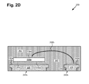
- Figure 2D illustrates a cross sectional view of a portion of PQFN package 200.
- the cross sectional view in Figure 2D corresponds to cross section 2D-2D, of Figures 2B and 2C .
- Figure 2D shows drain 236e of V-phase power switch 206a connected to common die pad 228 through conductive adhesive 254 and plating 248a of leadframe 260.
- Conductive adhesive 254 can include silver filled adhesive such as QMI 529HT.
- Other dies in PQFN package 200 can similarly be connected to leadframe 260.
- driver IC 202 is situated on driver IC die pad 220. More particularly, ground 256 of driver IC 202 is situated on driver IC die pad 220 of leadframe 260.
- Driver IC die pad 220 is larger than driver IC 202 and can therefore accommodate different, larger driver ICs, which may have different features than driver IC 202.
- Figure 2B also shows that wirebonds, such as wirebond 244a electrically and mechanically connect driver IC 202 to VCC terminal 212b, HIN1 terminal 212c, HIN2 terminal 212d, HIN3 terminal 212e, LIN1 terminal 212f, LIN2 terminal 212g, LIN3 terminal 212h, EN terminal 212i, FAULT terminal 212j, RCIN terminal 212k, IM terminal 2121, VSS terminal 212m, VB1 terminal 212r, VB2 terminal 212s, VB3 terminal 212t, and to respective gates of U-phase power switches 204a and 204b, V-phase power switches 206a and 206b, and W-phase power switches 208a and 208b.
- wirebonds such as wirebond 244a electrically and mechanically connect driver IC 202 to VCC terminal 212b, HIN1 terminal 212c, HIN2 terminal 212d, HIN3 terminal 212e, LIN1 terminal 212f, LIN2
- Wirebond 244a and similarly depicted wirebonds in Figure 2B can include, for example, 1.3 mil diameter G1 type Gold (Au) wires. Thicker wires can be utilized for power connections, such as wirebonds 246a, 246b, 246c, 246d, 246e, and 246f (also referred to as "wirebonds 246"). Wirebonds 246 can be, for example, 2.0 mil diameter copper (Cu) wires, such as Maxsoft® LD wires available from Kulicke & Soffa®. Wirebonds 246 can be bonded using bond stitch on ball (BSOB) bonding. As shown in Figure 2B , multiple wirebonds, such as two wirebonds, can be in parallel with wirebonds 246 to for additional current handling.
- BSOB bond stitch on ball
- wirebond 246f electrically and mechanically connects source 238c of U-phase power switch 204b and source 238b of V-phase power switch 206b.
- Wirebond 246e electrically and mechanically connects source 238b of V-phase power switch 206b and source 238a of W-phase power switch 208b.
- Wirebond 246d electrically and mechanically connects source 238a of W-phase power switch 208b and VCOM terminal 212n.
- sources 238a, 238b, and 238c are coupled to respective terminals using respective wirebonds. In other words, sources 238a, 238b, and 238c are not shorted to one another in PQFN package 200.
- wirebond 246a electrically and mechanically connects source 238d of U-phase power switch 204a to leadframe 260. More particularly, source 238d is connected via wirebond 246a to leadframe island 236 of leadframe strip 232.
- U-phase output node 110a of Figure 1A is situated on leadframe strip 232 of leadframe 260, where leadframe strip 232 is connected to U-phase die pad 222c of leadframe 260.
- PQFN package 200 has significant flexibility in arranging wirebond 246a, and other wirebonds, such as wirebond 244b, while avoiding wire shorts due to wire crossing and achieving high electrical and thermal performance.
- Wirebond 244b electrically and mechanically connects driver IC 202 and leadframe strip 232 of leadframe 260 at leadframe island 236 to provide SW1 to driver IC 202 as shown in Figure 1A .
- U-phase output node 110a of Figure 1A is also situated on leadframe island 236 of leadframe 260. As leadframe island 236 is exposed on bottom-side 240b of PQFN package 200 (shown in Figure 2C ), heat generated at U-phase output node 110a can be effectively dissipated from PQFN package 200.
- wirebond 246b electrically and mechanically connects source 238e of V-phase power switch 206a to leadframe 260.
- Figure 2D illustrates one example of this connection.
- Source 238e is connected via wirebond 246b to leadframe island 234 of leadframe strip 230 through plating 248b of leadframe 260.
- Leadframe strip 230 then connects to drain 236b of V-phase power switch 206b through V-phase die pad 222b.
- a similar connection can be employed for connecting source 238d to drain 236c of U-phase power switch 204b.
- Wirebond 246b electrically and mechanically connects source 238e of V-phase power switch 206a to leadframe strip 230 at leadframe island 234.
- V-phase output node 110b of Figure 1A is situated on leadframe strip 230 of leadframe 260, where leadframe strip 230 is connected to V-phase die pad 222b of leadframe 260.
- PQFN package 200 has significant flexibility in arranging wirebond 246b, and other wirebonds, such as wirebond 244c, while avoiding wire shorts due to wire crossing and achieving high electrical and thermal performance.
- Wirebond 244c electrically and mechanically connects driver IC 202 and leadframe strip 230 of leadframe 260 at leadframe island 234 to provide SW2 to driver IC 202 as shown in Figure 1A .
- V-phase output node 110b of Figure 1A is also situated on leadframe island 234 of leadframe 260. As leadframe island 234 is exposed on bottom-side 240b of PQFN package 200 (shown in Figure 2C ), heat generated at V-phase output node 110b can be effectively dissipated from PQFN package 200.
- Wirebond 246c electrically and mechanically connects source 238f of W-phase power switch 208a to leadframe 260. More particularly, wirebond 246b electrically and mechanically connects source 238f of W-phase power switch 208a to W-phase die pad 222a on leadframe 260.
- W-phase output node 110c of Figure 1A is situated on W-phase die pad 222a of leadframe 260 with W-phase power switch 208b.
- source 238f of W-phase power switch 208a can be coupled to drain 236a of W-phase power switch 208b while easily avoiding wire shorts due to wire crossing and achieving high electrical and thermal performance.
- PQFN package 200 can be made significantly smaller while avoiding arcing between U-phase output node 110a, V-phase output node 110b, and W-phase output node 110c.
- an additional leadframe strip and/or leadframe island would require a larger PQFN package 200 to maintain sufficient spacing 252 between leadframe strips 230 and 232 so as to prevent arcing (e.g. at least 1 mm).
- this configuration does not significantly impact flexibility in arranging wirebonds in PQFN package 200.
- Wirebond 244d electrically and mechanically connects driver IC 202 and source 238f to provide SW3 to driver IC 202 as shown in Figure 1A .
- a PQFN package includes at least one of a leadframe island and a leadframe strip. It is noted that the PQFN package can include the leadframe island without the leadframe strip. For example, leadframe island 234 can be connected to V-phase die pad 222b through a trace on a PCB. It is further noted that the PQFN package can include the leadframe strip without the leadframe island. However, having the leadframe strip with the leadframe island can offer significant flexibility in arranging wirebonds in the PQFN package while achieving high electrical and thermal performance. Thus, the PQFN package can readily support complex configurations, which may include a large number of electrical components.
Landscapes
- Inverter Devices (AREA)
- Lead Frames For Integrated Circuits (AREA)
- Physics & Mathematics (AREA)
- Geometry (AREA)
- Structures Or Materials For Encapsulating Or Coating Semiconductor Devices Or Solid State Devices (AREA)
Abstract
Description
- The present application claims the benefit of and priority to provisional application Serial No.
61/774,506, filed on March 7, 2013 13/662,244 filed on October 26, 2012 13/034,519 filed on February 24, 2011 61/459,527 filed on December 13, 2010 - As used herein, the phrase "group III-V" refers to a compound semiconductor including at least one group III element and at least one group V element. By way of example, a group III-V semiconductor may take the form of a III-Nitride semiconductor. "III-Nitride", or "III-N", refers to a compound semiconductor that includes nitrogen and at least one group III element such as aluminum (Al), gallium (Ga), indium (In), and boron (B), and including but not limited to any of its alloys, such as aluminum gallium nitride (AlxGa(1-x)N), indium gallium nitride (InyGa(1-y)N), aluminum indium gallium nitride (AlxInyGa(1-x-y)N), gallium arsenide phosphide nitride (GaAsaPbN(1-a-b)), aluminum indium gallium arsenide phosphide nitride (AlxInyGa(1-x-y)AsaPbN(1-a-b)), for example. III-Nitride also refers generally to any polarity including but not limited to Ga-polar, N-polar, semi-polar, or non-polar crystal orientations. A III-Nitride material may also include either the Wurtzitic, Zincblende, or mixed polytypes, and may include single-crystal, monocrystalline, polycrystalline, or amorphous structures. Gallium nitride or GaN, as used herein, refers to a III-Nitride compound semiconductor wherein the group III element or elements include some or a substantial amount of gallium, but may also include other group III elements in addition to gallium. A group III-V or a GaN transistor may also refer to a composite high voltage enhancement mode transistor that is formed by connecting the group III-V or the GaN transistor in cascode with a lower voltage group IV transistor.
- In addition, as used herein, the phrase "group IV" refers to a semiconductor that includes at least one group IV element such as silicon (Si), germanium (Ge), and carbon (C), and may also include compound semiconductors such as silicon germanium (SiGe) and silicon carbide (SiC), for example. Group IV also refers to semiconductor materials which include more than one layer of group IV elements, or doping of group IV elements to produce strained group IV materials, and may also include group IV based composite substrates such as silicon on insulator (SOI), separation by implantation of oxygen (SIMOX) process substrates, and silicon on sapphire (SOS), for example.
- Packages combining several semiconductor devices can simplify circuit design, reduce costs, and provide greater efficiency and improved performance by keeping related and dependent circuit components in close proximity. Furthermore, these packages can facilitate application integration and greater electrical and thermal performance compared to using separate packaging for components.
- Quad flat no-lead (QFN) packages are leadless packages for electrical components, such as power semiconductor devices. The QFN packages can utilize a leadframe and wirebonds for connection to the electrical components housed therein. The QFN packages often have limited complexity and electrical routing can be challenging, particularly for more complex configurations. Thus, QFN packages often have simple configurations and house a small number of electrical components.
- A power quad flat no-lead (PQFN) semiconductor package with leadframe islands for multi-phase power inverter, substantially as shown in and/or described in connection with at least one of the figures, and as set forth more completely in the claims.
-
-
Figure 1A illustrates a schematic diagram of an exemplary circuit of a power quad flat no-lead (PQFN) package. -
Figure 1B illustrates a schematic diagram of a PQFN package in an exemplary multi-phase power inverter circuit. -
Figure 2A illustrates a top-plan view of a leadframe of an exemplary PQFN package. -
Figure 2B illustrates a top-plan view of an exemplary PQFN package with wirebonds. -
Figure 2C illustrates a bottom-plan view of an exemplary PQFN package. -
Figure 2D illustrates a cross sectional view of a portion of an exemplary PQFN package. - The following description contains specific information pertaining to implementations in the present disclosure. The drawings in the present application and their accompanying detailed description are directed to merely exemplary implementations. Unless noted otherwise, like or corresponding elements among the figures may be indicated by like or corresponding reference numerals. Moreover, the drawings and illustrations in the present application are generally not to scale, and are not intended to correspond to actual relative dimensions.
-
Figure 1A illustrates a schematic diagram of an exemplary circuit of power quad flat no-lead (PQFN)package 100.Figure 1B illustrates a schematic diagram ofPQFN package 100 in multi-phasepower inverter circuit 150. - Referring to
Figures 1A and1B ,PQFN package 100 includes driver integrated circuit (IC) 102,U-phase power switches phase power switches phase power switches power inverter circuit 150 ofFigure 1B ,PQFN package 100 is connected tobus voltage source 114,supply voltage source 116,microcontroller 124,motor 126, resistor R1, capacitor C1, bootstrap capacitors CB1, CB2, CB3, and shunt resistor RS. Any ofPQFN package 100,microcontroller 124,motor 126, resistor R1, capacitor C1, bootstrap capacitors CB1, CB2, CB3, and shunt resistor RS can be mounted on a printed circuit board (PCB). Furthermore,PQFN package 100 can be connected to any ofbus voltage source 114,supply voltage source 116,microcontroller 124,motor 126, resistor R1, capacitor C1, bootstrap capacitors CB1, CB2, CB3, and shunt resistor RS through conductive leads on the PCB. -
PQFN package 100 also includes VBUSterminal 112a,VCC terminal 112b,HIN1 terminal 112c,HIN2 terminal 112d,HIN3 terminal 112e,LIN1 terminal 112f,LIN2 terminal 112g,LIN3 terminal 112h,EN terminal 112i, FAULTterminal 112j, RCINterminal 112k,IM terminal 1121,VSS terminal 112m, VCOMterminal 112n, SW1 terminal 112o,SW2 terminal 112p, SW3 terminal 112q,VB1 terminal 112r,VB2 terminal 112s, andVB3 terminal 112t, which are collectively referred to as I/O terminals 112. - In
PQFN package 100, VBUSterminal 112a receives VBUS as input frombus voltage source 114.VCC terminal 112b receives VCC as input to driver IC 102 fromsupply voltage source 116.HIN1 terminal 112c,HIN2 terminal 112d, andHIN3 terminal 112e receive HIN1, HIN2, and HIN3 respectively as inputs to driverIC 102 frommicrocontroller 124.LIN1 terminal 112f,LIN2 terminal 112g, andLIN3 terminal 112h receive LIN1, LIN2, and LIN3 respectively as inputs to driverIC 102 frommicrocontroller 124. ENterminal 112i receives EN as input to driver IC 102 frommicrocontroller 124.FAULT terminal 112j receives FAULT as output from driver IC 102 tomicrocontroller 124. RCINterminal 112k receives RCIN as input todriver IC 102 from resistor R1 and capacitor C1.IM terminal 1121 receives ITRIP as input to driver IC 102 andmicrocontroller 124 fromU-phase power switch 104b, V-phase power switch 106b, and W-phase power switch 108b.VSS terminal 112m receives VSS as input to driver IC 102 from logic ground GVSS. VCOMterminal 112n receives VCOM as input to driver IC 102,U-phase power switch 104b, V-phase power switch 106b, and W-phase power switch 108b from power ground GCOM. SW1 terminal 112o receives SW1 fromU-phase output node 110a as output tomotor 126. Driver IC 102 also receives SW1 as input fromU-phase output node 110a.SW2 terminal 112p receives SW2 from V-phase output node 110b as output tomotor 126. Driver IC 102 also receives SW2 as input from V-phase output node 110b. SW3 terminal 112q receives SW3 from W-phase output node 110c as output tomotor 126. Driver IC 102 also receives SW3 as input from W-phase output node 110c.VB1 terminal 112r receives VB1 as input to driverIC 102 from bootstrap capacitor CB1.VB2 terminal 112s receives VB2 as input to driverIC 102 from bootstrap capacitor CB2.VB3 terminal 112t receives VB3 as input to driverIC 102 from bootstrap capacitor CB3. - It will be appreciated that in various implementations, the number, quantity, and location of I/O terminals 112 are different than what is shown. For example, in various implementations, a driver IC that is different than driver IC 102 can be utilized, which can have different capabilities and/or I/O requirements than driver IC 102. This may be reflected in I/O terminals 112 as well as other connections of
PQFN package 100. As one specific example, in one implementation, driver IC 102 is instead a functionally integrated IC that incorporates functionality of driver IC 102 andmicrocontroller 124. Thus, additional I/O terminals 112 may be required for functionality ofmicrocontroller 124, while certain I/O terminals 112, such asFAULT terminal 112j may not be required. -
PQFN package 100 is for a multi-phase power inverter anddriver IC 102 can be a high voltage IC (HVIC) for drivingU-phase power switches phase power switches phase power switches driver IC 102 include "5th generation" HVICs available from International Rectifier Corporation®. In the present implementation,U-phase power switches phase power switches phase power switches U-phase power switches phase power switches phase power switches PQFN package 100 provides a full bridge power device, alternative implementations can provide other package configurations as required by the particular application. - In
PQFN package 100, HIN1, HIN2, and HIN3 are control signals forU-phase power switch 104a, V-phase power switch 106a, and W-phase power switch 108a, which are high side transistors.Driver IC 102 generates high side gate signals H1, H2, and H3 from HIN1, HIN2, and HIN3 respectively, which are then provided toU-phase power switch 104a, V-phase power switch 106a, and W-phase power switch 108a, as shown inFigure 1A . Similarly, LIN1, LIN2, and LIN3 are control signals forU-phase power switch 104b, V-phase power switch 106b, and W-phase power switch 108b, which are low side transistors.Driver IC 102 generates low side gate signals L1, L2, and L3 from LIN1, LIN2, and LIN3 respectively, which are then provided toU-phase power switch 104b, V-phase power switch 106b, and W-phase power switch 108b, as shown inFigure 1A . EN can be used, for example bymicrocontroller 124, to enable switching ofdriver IC 102. More particularly,driver IC 102 is configured to enable switching of H1, H2, H3, L1, L2, and L3 responsive to EN. - VBUS is a bus voltage from
bus voltage source 114, which is coupled to respective drains ofU-phase power switch 104a, V-phase power switch 106a, and W-phase power switch 108a. As one example,bus voltage source 114 can be an AC to DC rectifier. The AC can be, as one example, an outlet voltage, such as 230 volts. The DC voltage can be, for example, approximately 300 volts to approximately 400 volts for VBUS. - VCC is a supply voltage for
driver IC 102 fromsupply voltage source 116, which can be approximately 15 volts. In some implementations,supply voltage source 116 generates VCC from VBUS. VB1, VB2, and VB3 are bootstrap voltages fordriver IC 102 and are provided by bootstrap capacitors CB1, CB2, and CB3 respectively. Bootstrap capacitors CB1, CB2, and CB3 can be charged, for example, by VCC throughdriver IC 102. Bootstrap capacitor CB1 is coupled betweenVB1 terminal 112r and SW3 terminal 112q. Bootstrap capacitor CB2 is coupled between VB2 terminal 112s andSW2 terminal 112p. Bootstrap capacitor CB3 is coupled between VB3 terminal 112t and SW1 terminal 112o. - VSS is a logic ground for
driver IC 102 from logic ground GVSS. VCOM is a power ground fordriver IC 102 from power ground GCOM. Thus, in the present implementation,PQFN package 100 has separate grounds for logic and power. Using separate grounds for logic and power,PQFN package 100 is protected from latch up and noise malfunction, which otherwise can be caused by excess switching voltages fromU-phase power switches phase power switches phase power switches PQFN package 100 has a shared ground for logic and power. In these implementations,PQFN package 100 may have a single I/O terminal for ground. - Separate logic and power grounds are provided for in multi-phase
power inverter circuit 150 using shunt resistor RS. Shunt resistor RS is coupled across VSS terminal 112m and VCOM terminal 112n. Shunt resistor RS is also coupled to sources of each ofU-phase power switch 104b, V-phase power switch 106b, and W-phase power switch 108b through VCOM terminal 112n. Thus, motor current IM frommotor 126, shown inFigure 1A , is combined phase current fromU-phase power switch 104b, V-phase power switch 106b, and W-phase power switch 108b. Motor current IM is provided tomicrocontroller 124 throughIM terminal 1121.Microcontroller 124 utilizes motor current IM to reconstruct individual phase currents (U, V, and W) to control pulse-width modulation (PWM) by controlling HIN1, HIN2, HIN3, LIN1, LIN2, and LIN3. - As shown in
Figure 1A , motor current IM is also provided todriver IC 102 as ITRIP.Driver IC 102 utilizes ITRIP for overcurrent protection. For example ITRIP is compared to a reference value. If ITRIP exceeds the reference value,driver IC 102 detects an overcurrent condition. Furthermore,driver IC 102 indicates the overcurrent condition tomicrocontroller 124 by providing FAULT to FAULT terminal 112j.Driver IC 102 utilizes RCIN to automatically reset from the overcurrent protection. As shown inFigure 1B , resistor R1 is coupled between VCC terminal 112b and RCIN terminal 112k to charge capacitor C1. Capacitor C1 is coupled between RCIN terminal 112k and VSS terminal 112m. Resistor R1 and capacitor C1 can be changed to alter timing of automatic reset for the overcurrent protection. - Typical QFN packages have limited complexity with simple configurations and a small number of electrical components. For more complex configurations, it would be difficult to rout wires for connections while avoiding wire crossing and wire shorting. Moreover, long lengths of wiring would adversely affect electrical and thermal performance. However, PQFN packages, in accordance with various implementations of the present disclosure, can be substantially more complex than typical QFN packages while avoiding wire crossing and wire shorting and achieving high electrical and thermal performance.
- Turning to
Figures 2A ,2B , and2C ,Figure 2A illustrates a top-plan view of a leadframe ofPQFN package 200 ofFigures 2B and2C .Figure 2B illustrates a top-plan view ofPQFN package 200.Figure 2C illustrates a bottom-plan view ofPQFN package 200. In the present implementation,PQFN package 200 is a multi-chip module (MCM) PQFN package, which can have a footprint of approximately 12 mm by approximately 12 mm. In other implementations,PQFN package 200 can have a footprint of greater than 12 mm by 12 mm. In still other implementations,PQFN package 200 can have a footprint of less than 12 mm by 12 mm. -
PQFN package 200 corresponds toPQFN package 100 inFigures 1A and1B . For example,PQFN package 200 includesdriver IC 202,U-phase power switches phase power switches phase power switches driver IC 102,U-phase power switches phase power switches phase power switches Figure 1A . Furthermore,PQFN package 200 includesVBUS terminal 212a, VCC terminal 212b, HIN1 terminal 212c,HIN2 terminal 212d,HIN3 terminal 212e, LIN1 terminal 212f, LIN2 terminal 212g,LIN3 terminal 212h,EN terminal 212i,FAULT terminal 212j, RCIN terminal 212k,IM terminal 2121, VSS terminal 212m, VCOM terminal 212n, SW1 terminal 212o (also referred to as "U-phase output terminal 212o"),SW2 terminal 212p (also referred to as "V-phase output terminal 212p"),SW3 terminal 212q (also referred to as "W-phase output terminal 212q"),VB1 terminal 212r,VB2 terminal 212s, and VB3 terminal 212t (also referred to as "I/O terminals 212") corresponding respectively toVBUS terminal 112a, VCC terminal 112b, HIN1 terminal 112c,HIN2 terminal 112d,HIN3 terminal 112e, LIN1 terminal 112f, LIN2 terminal 112g,LIN3 terminal 112h,EN terminal 112i,FAULT terminal 112j, RCIN terminal 112k,IM terminal 1121, VSS terminal 112m, VCOM terminal 112n, SW1 terminal 112o,SW2 terminal 112p, SW3 terminal 112q,VB1 terminal 112r,VB2 terminal 112s, and VB3 terminal 112t inPQFN package 100. -
Figure 2A shows leadframe 260 including driver IC diepad 220, W-phase die pad 222a, V-phase die pad 222b,U-phase die pad 222c, andcommon die pad 228.Lead frame 260 further includes leadframe strips 230 and 232 and I/O terminals 212. -
Leadframe island 234 is onleadframe strip 230 ofleadframe 260 andleadframe strip 230 is electrically and mechanically connected (e.g. integrally connected) to V-phase die pad 222b ofleadframe 260.Leadframe island 236 is onleadframe strip 232 ofleadframe 260 andleadframe strip 232 is electrically and mechanically connected (e.g. integrally connected) toU-phase die pad 222c ofleadframe 260. As shown inFigure 2B , leadframe strips 230 and 232 can optionally extend to edge 242c ofPQFN package 200. In doing so, any of leadframe strips 230 and 232 can provide, for example, additional I/O terminals forPQFN package 200. For example,leadframe strip 232 is shown as providing an additional SW1 terminal 212o atedge 242c ofPQFN package 200. -
Leadframe 260 can comprise a material with high thermal and electrical conductivity such as copper (Cu) alloy C194 available from Olin Brass®. Top-side 240a ofleadframe 260 can be selectively plated with materials for enhanced adhesion to device dies and wires. The plating can comprise silver (Ag) plating that is selectively applied toleadframe 260, which is available from companies such as QPL Limited. -
Figures 2A and2B show that leadframe 260 is an etched leadframe, such as a halfetched leadframe. Portions ofleadframe 260, which are unetched (e.g. not half-etched) are indicated inFigures 2A and2B using dashed lines.Leadframe islands Figure 2C shows bottom-side 240b of leadframe 260 (which also corresponds to a bottom-side of PQFN package 200). -
Figure 2C further showsmold compound 265 ofPQFN package 200, which covers etched portions ofleadframe 260.Mold compound 265 can be a plastic that has a low flexural modulus, such as CEL9220ZHF10 (v79) available from Hitachi® Chemical. To provide resilience against package cracking, the height (or thickness) ofPQFN package 200 as defined bymold compound 265 may be kept thin, such as 0.9 mm or less. I/O terminals 212,leadframe island 234 andleadframe island 236 are unetched and are exposed throughmold compound 265 on bottom-side 240b of leadframe 260 (which also corresponds to a bottom-side of PQFN package 200). As such, I/O terminals 212,leadframe island 234 andleadframe island 236 are exposed on bottom-side 240b ofleadframe 260 for high electrical conductivity and/or thermal dissipation. By providing a (PCB) with matching lands, this feature can be exploited. The exposed areas ofleadframe 260 can be plated, for example with Tin (Sn). -
Driver IC 202,U-phase power switches phase power switches phase power switches leadframe 260. -
Figure 2B shows thatU-phase power switches phase power switches phase power switches driver IC 202 are electrically and mechanically connected toleadframe 260. This can be accomplished utilizing solder or conductive adhesive, such as silver filled QMI 529HT available from Henkel Corporation. - As shown in
Figure 2B ,U-phase power switch 204b, V-phase power switch 206b, and W-phase power switch 208b are situated alongedge 242a ofPQFN package 200. W-phase power switch 208b is situated on W-phase die pad 222a. More particularly,drain 236a of W-phase power switch 208b is situated on W-phase die pad 222a. Similarly, V-phase power switch 206b is situated on V-phase die pad 222b. More particularly,drain 236b of V-phase power switch 206b is situated on V-phase die pad 222b. Also,U-phase power switch 204b is situated onU-phase die pad 222c. More particularly,drain 236c ofU-phase power switch 204b is situated onU-phase die pad 222c. Thus,U-phase power switch 204b, V-phase power switch 206b, and W-phase power switch 208b are individually coupled to respective die pads ofleadframe 260. As such, W-phase die pad 222a can correspond to W-phase output terminal 212q ofPQFN package 200, V-phase die pad 222b can correspond to V-phase output terminal 212p ofPQFN package 200, and U-phase diepad 222c can correspond to U-phase output terminal 212o ofPQFN package 200, as shown inFigure 2B . - Also shown in
Figure 2B ,U-phase power switch 204a, V-phase power switch 206a, and W-phase power switch 208a are situated alongedge 242b ofPQFN package 200, which intersectsedge 242a.U-phase power switch 204a, V-phase power switch 206a, and W-phase power switch 208a are situated oncommon die pad 228. More particularly,drain 236d ofU-phase power switch 204a,drain 236e of V-phase power switch 206a, and drain 236f of W-phase power switch 208a are situated oncommon die pad 228 ofleadframe 260. Thus,common die pad 228 can correspond toVBUS terminal 212a (e.g. a bus voltage input terminal) ofPQFN package 200, as shown inFigure 2B . - An example of this configuration is shown in more detail in
Figure 2D. Figure 2D illustrates a cross sectional view of a portion ofPQFN package 200. The cross sectional view inFigure 2D corresponds to crosssection 2D-2D, ofFigures 2B and2C .Figure 2D showsdrain 236e of V-phase power switch 206a connected tocommon die pad 228 throughconductive adhesive 254 and plating 248a ofleadframe 260. Conductive adhesive 254 can include silver filled adhesive such as QMI 529HT. Other dies inPQFN package 200 can similarly be connected toleadframe 260. - As shown in
Figure 2B ,driver IC 202 is situated on driver IC diepad 220. More particularly,ground 256 ofdriver IC 202 is situated on driver IC diepad 220 ofleadframe 260. Driver IC diepad 220 is larger thandriver IC 202 and can therefore accommodate different, larger driver ICs, which may have different features thandriver IC 202. -
Figure 2B also shows that wirebonds, such as wirebond 244a electrically and mechanically connectdriver IC 202 to VCC terminal 212b, HIN1 terminal 212c,HIN2 terminal 212d,HIN3 terminal 212e, LIN1 terminal 212f, LIN2 terminal 212g,LIN3 terminal 212h,EN terminal 212i,FAULT terminal 212j, RCIN terminal 212k,IM terminal 2121, VSS terminal 212m,VB1 terminal 212r,VB2 terminal 212s, VB3 terminal 212t, and to respective gates ofU-phase power switches phase power switches phase power switches -
Wirebond 244a and similarly depicted wirebonds inFigure 2B can include, for example, 1.3 mil diameter G1 type Gold (Au) wires. Thicker wires can be utilized for power connections, such as wirebonds 246a, 246b, 246c, 246d, 246e, and 246f (also referred to as "wirebonds 246"). Wirebonds 246 can be, for example, 2.0 mil diameter copper (Cu) wires, such as Maxsoft® LD wires available from Kulicke & Soffa®. Wirebonds 246 can be bonded using bond stitch on ball (BSOB) bonding. As shown inFigure 2B , multiple wirebonds, such as two wirebonds, can be in parallel with wirebonds 246 to for additional current handling. - In
Figure 2B ,wirebond 246f electrically and mechanically connectssource 238c ofU-phase power switch 204b andsource 238b of V-phase power switch 206b.Wirebond 246e electrically and mechanically connectssource 238b of V-phase power switch 206b andsource 238a of W-phase power switch 208b.Wirebond 246d electrically and mechanically connectssource 238a of W-phase power switch 208b and VCOM terminal 212n. It is noted that in other implementations, such as open source implementations ofPQFN package 200,sources sources PQFN package 200. - Also in
Figure 2B , wirebond 246a electrically and mechanically connectssource 238d ofU-phase power switch 204a toleadframe 260. More particularly,source 238d is connected viawirebond 246a to leadframeisland 236 ofleadframe strip 232. Thus,U-phase output node 110a ofFigure 1A is situated onleadframe strip 232 ofleadframe 260, whereleadframe strip 232 is connected toU-phase die pad 222c ofleadframe 260. As such,PQFN package 200 has significant flexibility in arrangingwirebond 246a, and other wirebonds, such aswirebond 244b, while avoiding wire shorts due to wire crossing and achieving high electrical and thermal performance.Wirebond 244b electrically and mechanically connectsdriver IC 202 andleadframe strip 232 ofleadframe 260 atleadframe island 236 to provide SW1 todriver IC 202 as shown inFigure 1A .U-phase output node 110a ofFigure 1A is also situated onleadframe island 236 ofleadframe 260. Asleadframe island 236 is exposed on bottom-side 240b of PQFN package 200 (shown inFigure 2C ), heat generated atU-phase output node 110a can be effectively dissipated fromPQFN package 200. - Similarly,
wirebond 246b electrically and mechanically connectssource 238e of V-phase power switch 206a toleadframe 260.Figure 2D illustrates one example of this connection.Source 238e is connected viawirebond 246b to leadframeisland 234 ofleadframe strip 230 through plating 248b ofleadframe 260.Leadframe strip 230 then connects to drain 236b of V-phase power switch 206b through V-phase die pad 222b. A similar connection can be employed for connectingsource 238d to drain 236c ofU-phase power switch 204b.Wirebond 246b electrically and mechanically connectssource 238e of V-phase power switch 206a toleadframe strip 230 atleadframe island 234. Thus, V-phase output node 110b ofFigure 1A is situated onleadframe strip 230 ofleadframe 260, whereleadframe strip 230 is connected to V-phase die pad 222b ofleadframe 260. As such,PQFN package 200 has significant flexibility in arrangingwirebond 246b, and other wirebonds, such aswirebond 244c, while avoiding wire shorts due to wire crossing and achieving high electrical and thermal performance.Wirebond 244c electrically and mechanically connectsdriver IC 202 andleadframe strip 230 ofleadframe 260 atleadframe island 234 to provide SW2 todriver IC 202 as shown inFigure 1A . V-phase output node 110b ofFigure 1A is also situated onleadframe island 234 ofleadframe 260. Asleadframe island 234 is exposed on bottom-side 240b of PQFN package 200 (shown inFigure 2C ), heat generated at V-phase output node 110b can be effectively dissipated fromPQFN package 200. -
Wirebond 246c electrically and mechanically connectssource 238f of W-phase power switch 208a toleadframe 260. More particularly,wirebond 246b electrically and mechanically connectssource 238f of W-phase power switch 208a to W-phase die pad 222a onleadframe 260. Thus, W-phase output node 110c ofFigure 1A is situated on W-phase die pad 222a ofleadframe 260 with W-phase power switch 208b. As W-phase power switch 208b is adjacent to W-phase power switch 208a,source 238f of W-phase power switch 208a can be coupled to drain 236a of W-phase power switch 208b while easily avoiding wire shorts due to wire crossing and achieving high electrical and thermal performance. This can be accomplished without utilizing a leadframe strip and/or leadframe island. Thus,PQFN package 200 can be made significantly smaller while avoiding arcing betweenU-phase output node 110a, V-phase output node 110b, and W-phase output node 110c. For example, an additional leadframe strip and/or leadframe island would require alarger PQFN package 200 to maintainsufficient spacing 252 between leadframe strips 230 and 232 so as to prevent arcing (e.g. at least 1 mm). Furthermore, this configuration does not significantly impact flexibility in arranging wirebonds inPQFN package 200. Also, as W-phase die pad 222a is exposed on bottom-side 240b of PQFN package 200 (shown inFigure 2C ), heat generated at W-phase output node 110c can be effectively dissipated fromPQFN package 200.Wirebond 244d electrically and mechanically connectsdriver IC 202 andsource 238f to provide SW3 todriver IC 202 as shown inFigure 1A . - Thus, in various implementations, a PQFN package includes at least one of a leadframe island and a leadframe strip. It is noted that the PQFN package can include the leadframe island without the leadframe strip. For example,
leadframe island 234 can be connected to V-phase die pad 222b through a trace on a PCB. It is further noted that the PQFN package can include the leadframe strip without the leadframe island. However, having the leadframe strip with the leadframe island can offer significant flexibility in arranging wirebonds in the PQFN package while achieving high electrical and thermal performance. Thus, the PQFN package can readily support complex configurations, which may include a large number of electrical components. - From the above description it is manifest that various techniques can be used for implementing the concepts described in the present application without departing from the scope of those concepts. Moreover, while the concepts have been described with specific reference to certain implementations, a person of ordinary skill in the art would recognize that changes can be made in form and detail without departing from the scope of those concepts. As such, the described implementations are to be considered in all respects as illustrative and not restrictive. It should also be understood that the present application is not limited to the particular implementations described above, but many rearrangements, modifications, and substitutions are possible without departing from the scope of the present disclosure.
Claims (15)
- A power quad flat no-lead (PQFN) package comprising:a U-phase output node situated on a first leadframe island of a leadframe;a V-phase output node situated on a second leadframe island of said leadframe;a W-phase output node situated on a W-phase die pad of said leadframe.
- The PQFN package of claim 1, comprising a first W-phase power switch situated on said W-phase die pad.
- The PQFN package of claim 1, comprising at least one wirebond connected to said W-phase die pad.
- The PQFN package of claim 1, comprising at least one wirebond connecting a source of a second W-phase power switch to said W-phase die pad.
- The PQFN package of claim 1, comprising at least one wirebond connected to said first leadframe island of said leadframe.
- The PQFN package of claim 1, comprising at least one wirebond connected to said second leadframe island of said leadframe.
- The PQFN package of claim 1, wherein said first leadframe island is exposed on a bottom-side of said PQFN package.
- The PQFN package of claim 1, wherein said second leadframe island is exposed on a bottom-side of said PQFN package.
- The PQFN package of claim 1, wherein said W-phase die pad is a W-phase output terminal of said PQFN package.
- The PQFN package of claim 1, wherein said first leadframe island is on a first leadframe strip of said leadframe, said first leadframe strip connected to a U-phase die pad of said leadframe.
- The PQFN package of claim 1, wherein said second leadframe island is on a second leadframe strip of said leadframe, said second leadframe strip connected to a V-phase die pad of said leadframe.
- The PQFN package of claim 1, comprising a first U-phase power switch situated on a U-phase die pad of said leadframe and a first V-phase power switch situated on a V-phase die pad of said leadframe.
- The PQFN package of claim 1, comprising a second U-phase power switch, a second V-phase power switch, and a second W-phase power switch situated on a common die pad of said leadframe.
- The PQFN package of claim 1, wherein said U-phase, V-phase, and W-phase power switches comprise group III-V transistors.
- A power quad flat no-lead (PQFN) package comprising:a U-phase output node situated on a first leadframe strip of a leadframe, said first leadframe strip connected to a U-phase die pad of said leadframe;a V-phase output node situated on a second leadframe strip of said leadframe, said second leadframe strip connected to a V-phase die pad of said leadframe;a W-phase output node situated on a W-phase die pad of said leadframe.
Applications Claiming Priority (2)
| Application Number | Priority Date | Filing Date | Title |
|---|---|---|---|
| US201361774506P | 2013-03-07 | 2013-03-07 | |
| US14/102,316 US9362215B2 (en) | 2010-12-13 | 2013-12-10 | Power quad flat no-lead (PQFN) semiconductor package with leadframe islands for multi-phase power inverter |
Publications (2)
| Publication Number | Publication Date |
|---|---|
| EP2775519A2 true EP2775519A2 (en) | 2014-09-10 |
| EP2775519A3 EP2775519A3 (en) | 2017-11-15 |
Family
ID=49916928
Family Applications (1)
| Application Number | Title | Priority Date | Filing Date |
|---|---|---|---|
| EP13199756.1A Withdrawn EP2775519A3 (en) | 2013-03-07 | 2013-12-30 | Power quad flat no-lead (PQFN) semiconductor package with leadframe islands for multi-phase power inverter |
Country Status (5)
| Country | Link |
|---|---|
| EP (1) | EP2775519A3 (en) |
| JP (1) | JP6200820B2 (en) |
| KR (2) | KR20140110725A (en) |
| CN (1) | CN104037150A (en) |
| TW (1) | TWI557851B (en) |
Cited By (1)
| Publication number | Priority date | Publication date | Assignee | Title |
|---|---|---|---|---|
| EP3800659A1 (en) | 2019-10-02 | 2021-04-07 | Infineon Technologies Austria AG | Multiphase inverter apparatus |
Families Citing this family (3)
| Publication number | Priority date | Publication date | Assignee | Title |
|---|---|---|---|---|
| CN110323199B (en) * | 2019-07-31 | 2024-09-13 | 上海晶丰明源半导体股份有限公司 | A QFN packaging structure of a multi-island lead frame and a power conversion module |
| CN114188315B (en) * | 2021-12-01 | 2025-07-08 | 深圳市炫鼎光电科技有限公司 | Surface mounted lamp bead structure |
| TWI878079B (en) * | 2024-04-01 | 2025-03-21 | 英屬開曼群島商海珀電子股份有限公司 | Package structure of high electron mobility transistor |
Family Cites Families (7)
| Publication number | Priority date | Publication date | Assignee | Title |
|---|---|---|---|---|
| US6249024B1 (en) * | 1998-12-09 | 2001-06-19 | International Rectifier Corp. | Power module with repositioned positive and reduced inductance and capacitance |
| JP2001135765A (en) * | 1999-11-05 | 2001-05-18 | Hitachi Cable Ltd | Method and apparatus for manufacturing composite lead frame |
| US7298027B2 (en) * | 2004-09-02 | 2007-11-20 | International Rectifier Corporation | SMT three phase inverter package and lead frame |
| JP2011029262A (en) * | 2009-07-22 | 2011-02-10 | Daikin Industries Ltd | Power converter |
| JP5554056B2 (en) | 2009-12-14 | 2014-07-23 | 古河電気工業株式会社 | Group III nitride semiconductor device and method for manufacturing group III nitride semiconductor device |
| US8587101B2 (en) * | 2010-12-13 | 2013-11-19 | International Rectifier Corporation | Multi-chip module (MCM) power quad flat no-lead (PQFN) semiconductor package utilizing a leadframe for electrical interconnections |
| US20120256193A1 (en) * | 2011-04-08 | 2012-10-11 | Intersil Americas Inc. | Monolithic integrated capacitors for high-efficiency power converters |
-
2013
- 2013-12-30 EP EP13199756.1A patent/EP2775519A3/en not_active Withdrawn
-
2014
- 2014-01-17 TW TW103101807A patent/TWI557851B/en active
- 2014-01-23 KR KR1020140008301A patent/KR20140110725A/en not_active Ceased
- 2014-01-24 JP JP2014011545A patent/JP6200820B2/en active Active
- 2014-01-27 CN CN201410038717.5A patent/CN104037150A/en active Pending
-
2016
- 2016-08-09 KR KR1020160101369A patent/KR102041939B1/en active Active
Cited By (3)
| Publication number | Priority date | Publication date | Assignee | Title |
|---|---|---|---|---|
| EP3800659A1 (en) | 2019-10-02 | 2021-04-07 | Infineon Technologies Austria AG | Multiphase inverter apparatus |
| US11303222B2 (en) | 2019-10-02 | 2022-04-12 | Infineon Technologies Austria Ag | Multiphase inverter apparatus |
| US11979096B2 (en) | 2019-10-02 | 2024-05-07 | Infineon Technologies Austria Ag | Multiphase inverter apparatus having half-bridge circuits and a phase output lead for each half-bridge circuit |
Also Published As
| Publication number | Publication date |
|---|---|
| CN104037150A (en) | 2014-09-10 |
| KR20140110725A (en) | 2014-09-17 |
| KR20160100878A (en) | 2016-08-24 |
| KR102041939B1 (en) | 2019-11-07 |
| JP6200820B2 (en) | 2017-09-20 |
| JP2014179587A (en) | 2014-09-25 |
| TW201507068A (en) | 2015-02-16 |
| EP2775519A3 (en) | 2017-11-15 |
| TWI557851B (en) | 2016-11-11 |
Similar Documents
| Publication | Publication Date | Title |
|---|---|---|
| US10438876B2 (en) | Power quad flat no-lead (PQFN) package in a single shunt inverter circuit | |
| US9362215B2 (en) | Power quad flat no-lead (PQFN) semiconductor package with leadframe islands for multi-phase power inverter | |
| US9324646B2 (en) | Open source power quad flat no-lead (PQFN) package | |
| USRE41719E1 (en) | Power MOSFET with integrated drivers in a common package | |
| US9443795B2 (en) | Power quad flat no-lead (PQFN) package having bootstrap diodes on a common integrated circuit (IC) | |
| US9171837B2 (en) | Cascode circuit | |
| JP2025096516A (en) | Semiconductor Device | |
| CN107305877B (en) | Adaptive Molded Leadframe Package and Related Methods | |
| KR102041939B1 (en) | Power quad flat no-lead(pqfn) semiconductor package with leadframe islands for multi-phase power inverter | |
| US9449957B2 (en) | Control and driver circuits on a power quad flat no-lead (PQFN) leadframe | |
| EP2775520B1 (en) | Open source Power Quad Flat No-Lead (PQFN) leadframe | |
| EP2775518A2 (en) | Power Quad Flat No-Lead (PQFN) package in a single shunt inverter circuit | |
| EP2775521A2 (en) | Power Quad Flat No-Lead (PQFN) package having bootstrap diodes on a common integrated circuit (IC) |
Legal Events
| Date | Code | Title | Description |
|---|---|---|---|
| PUAI | Public reference made under article 153(3) epc to a published international application that has entered the european phase |
Free format text: ORIGINAL CODE: 0009012 |
|
| 17P | Request for examination filed |
Effective date: 20131230 |
|
| AK | Designated contracting states |
Kind code of ref document: A2 Designated state(s): AL AT BE BG CH CY CZ DE DK EE ES FI FR GB GR HR HU IE IS IT LI LT LU LV MC MK MT NL NO PL PT RO RS SE SI SK SM TR |
|
| AX | Request for extension of the european patent |
Extension state: BA ME |
|
| PUAL | Search report despatched |
Free format text: ORIGINAL CODE: 0009013 |
|
| AK | Designated contracting states |
Kind code of ref document: A3 Designated state(s): AL AT BE BG CH CY CZ DE DK EE ES FI FR GB GR HR HU IE IS IT LI LT LU LV MC MK MT NL NO PL PT RO RS SE SI SK SM TR |
|
| AX | Request for extension of the european patent |
Extension state: BA ME |
|
| RIC1 | Information provided on ipc code assigned before grant |
Ipc: H01L 23/495 20060101AFI20171009BHEP |
|
| RAP1 | Party data changed (applicant data changed or rights of an application transferred) |
Owner name: INFINEON TECHNOLOGIES AMERICAS CORP. |
|
| STAA | Information on the status of an ep patent application or granted ep patent |
Free format text: STATUS: THE APPLICATION IS DEEMED TO BE WITHDRAWN |
|
| 18D | Application deemed to be withdrawn |
Effective date: 20180516 |