EP2774000B1 - Procede anti-effets de charge pour la lithographie et la microscopie electronique - Google Patents
Procede anti-effets de charge pour la lithographie et la microscopie electronique Download PDFInfo
- Publication number
- EP2774000B1 EP2774000B1 EP12795496.4A EP12795496A EP2774000B1 EP 2774000 B1 EP2774000 B1 EP 2774000B1 EP 12795496 A EP12795496 A EP 12795496A EP 2774000 B1 EP2774000 B1 EP 2774000B1
- Authority
- EP
- European Patent Office
- Prior art keywords
- sacrificial layer
- layer
- resin
- conductive layer
- lithography
- Prior art date
- Legal status (The legal status is an assumption and is not a legal conclusion. Google has not performed a legal analysis and makes no representation as to the accuracy of the status listed.)
- Active
Links
- 238000000034 method Methods 0.000 title claims description 34
- 230000000694 effects Effects 0.000 title claims description 6
- 238000001459 lithography Methods 0.000 title description 9
- 238000001493 electron microscopy Methods 0.000 title description 2
- 239000011347 resin Substances 0.000 claims description 26
- 229920005989 resin Polymers 0.000 claims description 26
- 239000000758 substrate Substances 0.000 claims description 16
- 229910052751 metal Inorganic materials 0.000 claims description 10
- 239000002184 metal Substances 0.000 claims description 10
- 238000000151 deposition Methods 0.000 claims description 9
- 229910000476 molybdenum oxide Inorganic materials 0.000 claims description 9
- PQQKPALAQIIWST-UHFFFAOYSA-N oxomolybdenum Chemical compound [Mo]=O PQQKPALAQIIWST-UHFFFAOYSA-N 0.000 claims description 9
- ZOKXTWBITQBERF-UHFFFAOYSA-N Molybdenum Chemical compound [Mo] ZOKXTWBITQBERF-UHFFFAOYSA-N 0.000 claims description 8
- XLYOFNOQVPJJNP-UHFFFAOYSA-N water Substances O XLYOFNOQVPJJNP-UHFFFAOYSA-N 0.000 claims description 8
- 229910052750 molybdenum Inorganic materials 0.000 claims description 7
- 239000011733 molybdenum Substances 0.000 claims description 7
- MHAJPDPJQMAIIY-UHFFFAOYSA-N Hydrogen peroxide Chemical compound OO MHAJPDPJQMAIIY-UHFFFAOYSA-N 0.000 claims description 6
- YBMRDBCBODYGJE-UHFFFAOYSA-N germanium oxide Inorganic materials O=[Ge]=O YBMRDBCBODYGJE-UHFFFAOYSA-N 0.000 claims description 3
- 239000000463 material Substances 0.000 claims description 3
- PVADDRMAFCOOPC-UHFFFAOYSA-N oxogermanium Chemical compound [Ge]=O PVADDRMAFCOOPC-UHFFFAOYSA-N 0.000 claims description 3
- 239000010953 base metal Substances 0.000 claims description 2
- 239000010410 layer Substances 0.000 description 42
- 230000008901 benefit Effects 0.000 description 8
- 239000011810 insulating material Substances 0.000 description 7
- 238000010894 electron beam technology Methods 0.000 description 6
- 238000004626 scanning electron microscopy Methods 0.000 description 6
- 230000008030 elimination Effects 0.000 description 5
- 238000003379 elimination reaction Methods 0.000 description 5
- 230000001066 destructive effect Effects 0.000 description 4
- 238000005240 physical vapour deposition Methods 0.000 description 4
- 230000008569 process Effects 0.000 description 4
- 239000011521 glass Substances 0.000 description 3
- 239000003795 chemical substances by application Substances 0.000 description 2
- 230000008021 deposition Effects 0.000 description 2
- PCHJSUWPFVWCPO-UHFFFAOYSA-N gold Chemical compound [Au] PCHJSUWPFVWCPO-UHFFFAOYSA-N 0.000 description 2
- 229910052737 gold Inorganic materials 0.000 description 2
- 239000010931 gold Substances 0.000 description 2
- 229960002163 hydrogen peroxide Drugs 0.000 description 2
- 230000006872 improvement Effects 0.000 description 2
- 238000004519 manufacturing process Methods 0.000 description 2
- 229920003229 poly(methyl methacrylate) Polymers 0.000 description 2
- 239000004926 polymethyl methacrylate Substances 0.000 description 2
- OKTJSMMVPCPJKN-UHFFFAOYSA-N Carbon Chemical compound [C] OKTJSMMVPCPJKN-UHFFFAOYSA-N 0.000 description 1
- BQCADISMDOOEFD-UHFFFAOYSA-N Silver Chemical compound [Ag] BQCADISMDOOEFD-UHFFFAOYSA-N 0.000 description 1
- 241001639412 Verres Species 0.000 description 1
- 230000004075 alteration Effects 0.000 description 1
- 229910052782 aluminium Inorganic materials 0.000 description 1
- XAGFODPZIPBFFR-UHFFFAOYSA-N aluminium Chemical compound [Al] XAGFODPZIPBFFR-UHFFFAOYSA-N 0.000 description 1
- 238000010719 annulation reaction Methods 0.000 description 1
- 229910052799 carbon Inorganic materials 0.000 description 1
- 231100000481 chemical toxicant Toxicity 0.000 description 1
- 239000004020 conductor Substances 0.000 description 1
- 238000010586 diagram Methods 0.000 description 1
- 238000004090 dissolution Methods 0.000 description 1
- 230000005684 electric field Effects 0.000 description 1
- 238000000609 electron-beam lithography Methods 0.000 description 1
- 229910052732 germanium Inorganic materials 0.000 description 1
- GNPVGFCGXDBREM-UHFFFAOYSA-N germanium atom Chemical compound [Ge] GNPVGFCGXDBREM-UHFFFAOYSA-N 0.000 description 1
- 230000002452 interceptive effect Effects 0.000 description 1
- 238000000879 optical micrograph Methods 0.000 description 1
- 238000002360 preparation method Methods 0.000 description 1
- 230000009467 reduction Effects 0.000 description 1
- 229910052709 silver Inorganic materials 0.000 description 1
- 239000004332 silver Substances 0.000 description 1
- 239000002356 single layer Substances 0.000 description 1
- 230000007928 solubilization Effects 0.000 description 1
- 238000005063 solubilization Methods 0.000 description 1
- 230000003381 solubilizing effect Effects 0.000 description 1
- 238000003860 storage Methods 0.000 description 1
- 239000000126 substance Substances 0.000 description 1
- 239000003440 toxic substance Substances 0.000 description 1
Images


Classifications
-
- G—PHYSICS
- G03—PHOTOGRAPHY; CINEMATOGRAPHY; ANALOGOUS TECHNIQUES USING WAVES OTHER THAN OPTICAL WAVES; ELECTROGRAPHY; HOLOGRAPHY
- G03F—PHOTOMECHANICAL PRODUCTION OF TEXTURED OR PATTERNED SURFACES, e.g. FOR PRINTING, FOR PROCESSING OF SEMICONDUCTOR DEVICES; MATERIALS THEREFOR; ORIGINALS THEREFOR; APPARATUS SPECIALLY ADAPTED THEREFOR
- G03F7/00—Photomechanical, e.g. photolithographic, production of textured or patterned surfaces, e.g. printing surfaces; Materials therefor, e.g. comprising photoresists; Apparatus specially adapted therefor
- G03F7/20—Exposure; Apparatus therefor
- G03F7/2051—Exposure without an original mask, e.g. using a programmed deflection of a point source, by scanning, by drawing with a light beam, using an addressed light or corpuscular source
- G03F7/2059—Exposure without an original mask, e.g. using a programmed deflection of a point source, by scanning, by drawing with a light beam, using an addressed light or corpuscular source using a scanning corpuscular radiation beam, e.g. an electron beam
-
- G—PHYSICS
- G03—PHOTOGRAPHY; CINEMATOGRAPHY; ANALOGOUS TECHNIQUES USING WAVES OTHER THAN OPTICAL WAVES; ELECTROGRAPHY; HOLOGRAPHY
- G03F—PHOTOMECHANICAL PRODUCTION OF TEXTURED OR PATTERNED SURFACES, e.g. FOR PRINTING, FOR PROCESSING OF SEMICONDUCTOR DEVICES; MATERIALS THEREFOR; ORIGINALS THEREFOR; APPARATUS SPECIALLY ADAPTED THEREFOR
- G03F7/00—Photomechanical, e.g. photolithographic, production of textured or patterned surfaces, e.g. printing surfaces; Materials therefor, e.g. comprising photoresists; Apparatus specially adapted therefor
- G03F7/004—Photosensitive materials
- G03F7/09—Photosensitive materials characterised by structural details, e.g. supports, auxiliary layers
- G03F7/11—Photosensitive materials characterised by structural details, e.g. supports, auxiliary layers having cover layers or intermediate layers, e.g. subbing layers
-
- H—ELECTRICITY
- H01—ELECTRIC ELEMENTS
- H01J—ELECTRIC DISCHARGE TUBES OR DISCHARGE LAMPS
- H01J2237/00—Discharge tubes exposing object to beam, e.g. for analysis treatment, etching, imaging
- H01J2237/26—Electron or ion microscopes
- H01J2237/28—Scanning microscopes
- H01J2237/2809—Scanning microscopes characterised by the imaging problems involved
-
- H—ELECTRICITY
- H01—ELECTRIC ELEMENTS
- H01J—ELECTRIC DISCHARGE TUBES OR DISCHARGE LAMPS
- H01J2237/00—Discharge tubes exposing object to beam, e.g. for analysis treatment, etching, imaging
- H01J2237/30—Electron or ion beam tubes for processing objects
- H01J2237/317—Processing objects on a microscale
- H01J2237/3175—Lithography
- H01J2237/31752—Lithography using particular beams or near-field effects, e.g. STM-like techniques
- H01J2237/31754—Lithography using particular beams or near-field effects, e.g. STM-like techniques using electron beams
-
- H—ELECTRICITY
- H01—ELECTRIC ELEMENTS
- H01J—ELECTRIC DISCHARGE TUBES OR DISCHARGE LAMPS
- H01J2237/00—Discharge tubes exposing object to beam, e.g. for analysis treatment, etching, imaging
- H01J2237/30—Electron or ion beam tubes for processing objects
- H01J2237/317—Processing objects on a microscale
- H01J2237/3175—Lithography
- H01J2237/31793—Problems associated with lithography
- H01J2237/31796—Problems associated with lithography affecting resists
Definitions
- the present invention relates to a treatment method applied to insulating materials which aims to avoid or limit the charging effects occurring on these materials when exposed to an electron beam. It also relates to a system comprising means arranged to implement such a method.
- the invention is applicable for treating more or less insulating materials subjected to an electron beam in general, and more particularly for the electronic lithography of resins on insulating substrates and for observation by scanning electron microscopy of insulating units. and / or resin on all types of substrates.
- the more or less insulating nature of certain substrates and the number of resins and insulating units can cause difficulties when irradiated with an electron beam, whether for example for the electronic writing in lithography, or for the observation by scanning electron microscopy. Indeed, a part of the electrons of the beam is trapped by the insulating substrate or the resin and thereby creates an electric field which deflects the incident electrons. This deflection may cause, in the case of direct electronic writing, errors in the positioning of the patterns on the insulating substrate, or, in the case of the observation, a distortion in the image obtained. These difficulties can be troublesome for the reliability and the precision, and can constitute a limiting factor for the improvement of the resolutions.
- a method of covering the sample with a thin conductive layer to increase its conductivity is used.
- This technique can be used for both electron beam lithography and scanning electron microscopy.
- An object of the invention is to overcome the disadvantages of the state of the art.
- the invention therefore proposes depositing a bilayer of distinct materials on a support formed by an insulating substrate or a resin.
- An advantage of the sacrificial layer is its possible elimination by a simple means without causing the sample to be spoiled, and its removal also causes that of the upper conductive layer. It is therefore a simple, non-binding and non-destructive means for the sample to reduce the effects of charge during irradiation by the electron beam.
- the deposition of the bilayer can be carried out by known methods, for example a PVD (Physical Vapor Deposition) type process.
- PVD Physical Vapor Deposition
- the bilayer is deposited on the insulating substrate covered with resin, then after exposure, the bilayer is removed by solubilizing the sacrificial layer in a suitable bath.
- the bilayer is deposited on the insulating material before its observation by scanning electron microscopy. After observation, the bilayer is removed by solubilization of the sacrificial layer.
- the insulating material is a resin
- the advantage of this technique is to leave the resin intact to then make another use. Another advantage is the possibility of using all types of substrates, insulating or not, which brings flexibility and homogeneity of processes.
- the sacrificial layer may consist of molybdenum oxide or germanium oxide, pure or in majority concentration.
- the elimination of the sacrificial layer can be carried out at room temperature.
- the conductive layer may be predominantly, or even exclusively, made of a metal, for example molybdenum, gold, silver, carbon or aluminum.
- the sacrificial layer and the metal layer are predominantly, or even exclusively, formed from the same base metal.
- the sacrificial layer is predominantly made of molybdenum oxide and the metal layer is predominantly molybdenum.
- Molybdenum oxide has the advantage of being removable with water.
- the sacrificial layer and the metal layer may be combined into a single layer, mainly or even exclusively composed of hydrogen-peroxide removable molybdenum.
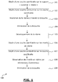
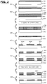
- the process 100 represented on the Figure 1 comprises a step 101 of deposition by a PVD method of a sacrificial layer 203 consisting of molybdenum oxide, on a support consisting of an insulating substrate 202 made of glass covered with a layer of PMMA resin 201 (polymethyl methacrylate).
- the thickness of the sacrificial layer 203 may be typically between 3 and 30 nm and preferably between 5 and 20 nm.
- This step 101 is followed by a step 102 of depositing a conductive layer 204 of molybdenum by a PVD process.
- the thickness of the conductive layer may be typically between 3 and 30 nm and preferably between 3 and 20 nm.
- the resin 201 is insolated in step 103 through the bilayer by interposing a mask to define the areas to be exposed to the electron beam.
- step 104 the bilayer is removed with water, to be able to develop the resin 201 in step 105.
- the method has already made it possible to produce the electronic part 103 of the lithography in the presence of the conducting layer 204, and therefore with a better precision.
- Step 106 is again a step of depositing a sacrificial layer 203 ', but this time on the resin patterns 201a to 201c obtained.
- This sacrificial layer 203 'with a thickness of 5 nm is molybdenum oxide.
- a conductive layer 204 ' On this layer of molybdenum oxide is deposited in step 107 a conductive layer 204 'with a thickness of 5 nm made of metal.
- This metal may be molybdenum, which then has the advantage of good compatibility with the sacrificial layer.
- the conductive layer 204 ' may also be made of gold, which has the advantage of being a better conductor than molybdenum.
- step 108 the resin patterns 201a to 201c are observed by scanning electron microscopy in the presence of the conductive layer 204 ', thus allowing an improvement in the quality of the image obtained.
- step 109 the bilayer is dissolved in water.
- the sample is stripped of the bilayer 203 ', 204', and thus ready for use, which makes the previous step 108 of observation non-destructive.
- this observation 108 may be used on an intermediate state without interfering with the overall manufacturing process. It is then possible to continue a manufacturing process, for example with a deposit of new layers followed by new stages of lithography.
- the figure 3 is an example of observation of resin patterns obtained according to the method 100, during the observation step 108.
- An interest of the bilayer is based on the fact that the resin patterns are then "reusable" because not altered by the elimination of the bilayer.
- the figure 4 is an optical microscope image of a lithographed glass sample after preparation of the resin patterns according to method 100.
Landscapes
- Physics & Mathematics (AREA)
- General Physics & Mathematics (AREA)
- Engineering & Computer Science (AREA)
- Architecture (AREA)
- Structural Engineering (AREA)
- Health & Medical Sciences (AREA)
- Toxicology (AREA)
- Electron Beam Exposure (AREA)
Description
- La présente invention concerne un procédé de traitement appliqué à des matériaux isolants qui a pour but d'éviter ou de limiter les effets de charge se produisant sur ces matériaux lorsqu'ils sont exposés à un faisceau électronique. Elle concerne également un système comprenant des moyens agencés pour mettre en oeuvre un tel procédé.
- L'invention est applicable pour traiter des matériaux plus ou moins isolants soumis à un faisceau d'électrons de façon générale, et plus particulièrement pour la lithographie électronique des résines sur des substrats isolants et pour l'observation par microscopie électronique à balayage de motifs isolants et/ou de résine sur tous types de substrats.
- Le caractère plus ou moins isolant de certains substrats et de nombres de résines et de motifs isolants peut causer des difficultés lors de leur irradiation par un faisceau d'électrons, que ce soit par exemple pour l'écriture électronique en lithographie, ou pour l'observation par microscopie électronique à balayage. En effet, une partie des électrons du faisceau est piégée par le substrat isolant ou la résine et crée de ce fait un champ électrique qui dévie les électrons incidents. Cette déviation peut entraîner, dans le cas de l'écriture électronique directe, des erreurs de positionnement des motifs sur le substrat isolant, ou, dans le cas de l'observation, une distorsion dans l'image obtenue. Ces difficultés peuvent être gênantes pour la fiabilité et la précision, et peuvent constituer un facteur limitant pour l'amélioration des résolutions.
- Pour remédier à ce problème, un procédé consistant à couvrir l'échantillon d'une fine couche conductrice pour augmenter sa conductivité est utilisé. En particulier, il est d'usage de déposer une fine couche conductrice d'une épaisseur de quelques nm, sur le substrat isolant ou la résine.
- Cette technique est utilisable aussi bien pour la lithographie à faisceau d'électrons que pour la microscopie électronique à balayage.
- Pour la lithographie, la fine couche conductrice déposée peut être de deux types :
- une couche métallique qui peut être placée soit sous la résine, soit au-dessus de la résine.
- Une résine conductrice (Exemple de l'ESPACER 300 commercialisé par la société Denko Showa), à placer sur le substrat isolant ou la résine, qui présente l'avantage d'être soluble dans l'eau.
- Mais ces techniques présentent des inconvénients. Dans le cas d'une couche métallique, l'utilisation d'une solution chimique pour l'éliminer est nécessaire et peut entrainer une altération de l'échantillon. Concernant les résines conductrices, ce sont des solutions chimiques corrosives et toxiques, qui ne sont pas compatibles avec tous les types de support. De plus, leurs conditions de stockage et d'utilisation sont très contraignantes pour des raisons de sécurité, ce qui entraîne des complexités et des coûts supplémentaires.
- Pour l'observation par microscopie électronique, une fine couche métallique est déposée sur les matériaux isolants. Mais cette technique peut être considérée comme destructrice pour l'échantillon puisqu'elle en change la nature, ou parce qu'il faudrait là aussi une solution corrosive pour la retirer.
- Un but de l'invention est de pallier les inconvénients de l'état de la technique.
- Plus particulièrement, un but de l'invention est de proposer une méthode non destructrice pour l'échantillon qui soit moins contraignante à mettre en oeuvre, tout en visant une annulation ou une limitation des effets de charge, et en particulier :
- une annulation ou une diminution des erreurs de positionnement des motifs sur le substrat,
- un meilleur réglage lors de la mise au point du faisceau électronique sur l'échantillon.
- L'invention propose d'atteindre au moins l'un de ces buts par un procédé de traitement pour éviter ou limiter les effets de charge sur un support formé par un substrat isolant ou une résine et destiné à être soumis à une irradiation électronique, caractérisé en ce qu'il comprend les étapes suivantes :
- dépôt d'une couche sacrificielle non conductrice sur le substrat ou la résine,
- dépôt d'une couche conductrice sur la couche sacrificielle,
- irradiation électronique pour lithographie ou observation,
- élimination de la couche sacrificielle et de la couche conductrice.
- L'invention propose donc de réaliser le dépôt d'une bicouche de matériaux distincts sur un support formé par un substrat isolant ou une résine. Un intérêt que présente la couche sacrificielle est son élimination possible par un moyen simple sans entrainer d'altération de l'échantillon, et que son élimination entraîne également celle de la couche conductrice supérieure. C'est donc un moyen simple, non contraignant et non destructeur pour l'échantillon pour diminuer les effets de charge lors de l'irradiation par le faisceau d'électrons.
- Cette méthode peut être avantageuse en particulier pour deux types d'utilisations :
- a) la lithographie électronique sur matériaux isolants,
- b) l'observation par microscopie électronique à balayage de matériaux isolants.
- Le dépôt de la bicouche peut être réalisé par des procédés connus, par exemple un procédé de type PVD (« Physical Vapor Deposition »).
- Dans le cas de la lithographie électronique, la bicouche est déposée sur le substrat isolant recouvert de résine, puis après insolation, la bicouche est éliminée en solubilisant la couche sacrificielle dans un bain approprié.
- Dans le cas de l'observation, la bicouche est déposée sur le matériau isolant avant son observation par microscopie électronique à balayage. Après observation, la bicouche est éliminée par solubilisation de la couche sacrificielle. Dans le cas particulier où le matériau isolant est une résine, l'avantage que présente cette technique est de laisser la résine intacte pour pouvoir ensuite en faire une autre utilisation. Un autre avantage est la possibilité d'utiliser tous types de substrats, isolants ou non, ce qui apporte souplesse et homogénéité des processus.
- Selon l'invention, la couche sacrificielle peut être constituée d'oxyde de molybdène ou d'oxyde de germanium, pur ou en concentration majoritaire.
- Dans le cas où la couche sacrificielle est constituée majoritairement de :
- oxyde de molybdène, l'étape d'élimination de la couche sacrificielle peut être réalisée avec de l'eau,
- oxyde de germanium, l'agent d'élimination peut être du peroxyde d'hydrogène.
- L'élimination de la couche sacrificielle peut se réaliser de la température ambiante. Pour faciliter l'élimination de la couche sacrificielle par l'eau lorsque la couche sacrificielle est particulièrement fine (< 10 nm), il peut être utile d'augmenter la température de dissolution, par exemple jusqu'à 40 °C.
- Selon l'invention, la couche conductrice peut être majoritairement, voire exclusivement, constituée d'un métal, par exemple le molybdène, l'or, l'argent, le carbone ou l'aluminium.
- Avantageusement, la couche sacrificielle et la couche métallique sont majoritairement, voire exclusivement, formées à partir d'un même métal de base.
- Selon un exemple de réalisation préféré, la couche sacrificielle est majoritairement constituée d'oxyde de molybdène et la couche métallique majoritairement de molybdène. L'oxyde de molybdène présente l'avantage d'être éliminable à l'eau.
- Selon un autre mode de réalisation, couche sacrificielle et couche métallique peuvent être confondues en une seule couche majoritairement voire exclusivement constituée de molybdène éliminable au peroxyde d'hydrogène.
- Des modes de réalisation variés de l'invention sont prévus, intégrant selon l'ensemble de leurs combinaisons possibles les différentes caractéristiques optionnelles exposées ici.
- D'autres particularités et avantages de l'invention ressortiront de la description détaillée d'un mode de mise en oeuvre nullement limitatif, et des dessins annexés sur lesquels :
- la
Figure 1 est une représentation sous la forme d'un diagramme d'un exemple de mise en oeuvre du procédé selon l'invention. - la
Figure 2 est une représentation schématique, selon une vue en coupe non à l'échelle, de différentes étapes d'un exemple de mise en oeuvre du procédé selon l'invention. - la
Figure 3 est une photo d'un exemple d'observation à deux échelles différentes de motifs en résine obtenus selon le procédé présenté en exemple dans laFigure 1 . - la
Figure 4 est un exemple de résultat obtenu sur un substrat de verre lithographié selon le procédé présenté en exemple dans laFigure 1 . - Le procédé 100 représenté sur la
Figure 1 comprend une étape 101 de dépôt par un procédé PVD d'une couche sacrificielle 203 constituée d'oxyde de molybdène, sur un support constitué d'un substrat isolant 202 en verre recouvert d'une couche de résine PMMA 201 (polyméthacrylate de méthyle). L'épaisseur de la couche sacrificielle 203 peut être comprise typiquement entre 3 et 30 nm et de préférence entre 5 et 20 nm. - Cette étape 101 est suivie d'une étape 102 de dépôt d'une couche conductrice 204 en molybdène par un procédé PVD. L'épaisseur de la couche conductrice peut être comprise typiquement entre 3 et 30 nm et de préférence entre 3 et 20 nm.
- Une fois la bicouche 203, 204 déposée sur le support 202, la résine 201 est insolée à l'étape 103 à travers la bicouche en intercalant un masque pour définir les zones à exposer au faisceau électronique.
- A l'étape 104, la bicouche est éliminée à l'eau, pour pouvoir développer la résine 201 à l'étape 105.
- A ce stade, on voit que le procédé a déjà permis de réaliser la partie électronique 103 de la lithographie en présence de la couche conductrice 204, et donc avec une meilleure précision.
- L'étape 106 est à nouveau une étape de dépôt d'une couche sacrificielle 203', mais cette fois-ci sur les motifs en résine obtenus 201a à 201c. Cette couche sacrificielle 203' d'une épaisseur de 5 nm est de l'oxyde de molybdène.
- Sur cette couche d'oxyde de molybdène, est déposée à l'étape 107 une couche conductrice 204' d'une épaisseur de 5 nm constituée de métal. Ce métal peut être du molybdène, qui présente alors l'avantage d'une bonne compatibilité avec la couche sacrificielle. La couche conductrice 204' peut aussi être faite d'or, qui présente l'avantage d'être meilleur conducteur que le molybdène.
- A l'étape 108, les motifs en résine 201a à 201c sont observés par microscopie électronique à balayage en présence de la couche conductrice 204', permettant ainsi une amélioration de la qualité de l'image obtenue.
- A l'étape 109, la bicouche est dissoute dans l'eau.
- A ce stade, l'échantillon est débarrassé de la bicouche 203', 204', et donc prêt à être utilisé, ce qui rend bien non destructive l'étape précédente 108 d'observation.
- Par exemple, cette observation 108 peut être utilisée sur un état intermédiaire sans interférer avec le processus global de fabrication. Il est alors possible de continuer un processus de fabrication, par exemple avec un dépôt de nouvelles couches suivi de nouvelles étapes de lithographie.
- La
figure 3 est un exemple d'observation de motifs en résine obtenus selon le procédé 100, lors de l'étape d'observation 108. Un intérêt de la bicouche repose sur le fait que les motifs en résine sont ensuite « réutilisables » car non altérés par l'élimination de la bicouche. - La
figure 4 est une image au microscope optique d'un échantillon en verre lithographié après préparation des motifs en résine selon le procédé 100. - Bien sûr, l'invention n'est pas limitée aux exemples qui viennent d'être décrits et de nombreux aménagements peuvent être apportés à ces exemples sans sortir du cadre de l'invention.
Claims (10)
- Procédé de traitement (100) pour éviter ou limiter les effets de charge sur un support formé par un substrat isolant ou une résine et destiné à être soumis à une irradiation électronique, caractérisé en ce qu'il comprend :- une étape de dépôt (101) d'une couche sacrificielle (203, 203') non conductrice,- une étape de dépôt (102) d'une couche conductrice (204, 204') sur ladite couche sacrificielle (203, 203'), lesdites couche sacrificielle et couche conductrice étant constituées de deux matériaux distincts,- une étape d'irradiation électronique (103),- une étape d'élimination(104) de la couche sacrificielle (203, 203').
- Procédé selon la revendication 1, caractérisé en ce que la couche sacrificielle (203, 203') est majoritairement constituée d'oxyde de molybdène.
- Procédé selon la revendication 2, caractérisé en ce que la couche sacrificielle (203, 203') est éliminée à l'eau.
- Procédé selon la revendication 3 caractérisé en ce que l'étape d'élimination (104, 109) de la couche sacrificielle (203, 203') est réalisée à une température comprise entre 25 et 40°C.
- Procédé selon la revendication 1, caractérisé en ce que la couche sacrificielle (203, 203') est majoritairement constituée d'oxyde de germanium.
- Procédé selon l'une quelconque des revendications 2 à 4, caractérisé en ce que la couche sacrificielle (203, 203') est éliminée au peroxyde d'hydrogène.
- Procédé selon l'une quelconque des revendications précédentes, caractérisé en ce que la couche conductrice (204, 204') est majoritairement constituée de métal.
- Procédé selon l'une quelconque des revendications précédentes, caractérisé en ce que la couche sacrificielle (203, 203') et la couche conductrice (204, 204') sont majoritairement formées à partir d'un même métal de base.
- Procédé selon l'une quelconque des revendications précédentes, caractérisé en ce que la couche sacrificielle (203, 203') est de l'oxyde de molybdène éliminable à l'eau et la couche conductrice (204, 204') est majoritairement constituée de molybdène.
- Système comprenant des moyens agencés pour mettre en oeuvre le procédé (100) selon l'une quelconque des revendications 1 à 9.
Applications Claiming Priority (2)
| Application Number | Priority Date | Filing Date | Title |
|---|---|---|---|
| FR1159890A FR2982044B1 (fr) | 2011-11-02 | 2011-11-02 | Procede anti-effets de charge pour la lithographie et la microscopie electronique. |
| PCT/FR2012/052520 WO2013064782A1 (fr) | 2011-11-02 | 2012-10-30 | Procede anti-effets de charge pour la lithographie et la microscopie electronique |
Publications (2)
| Publication Number | Publication Date |
|---|---|
| EP2774000A1 EP2774000A1 (fr) | 2014-09-10 |
| EP2774000B1 true EP2774000B1 (fr) | 2017-09-06 |
Family
ID=47291091
Family Applications (1)
| Application Number | Title | Priority Date | Filing Date |
|---|---|---|---|
| EP12795496.4A Active EP2774000B1 (fr) | 2011-11-02 | 2012-10-30 | Procede anti-effets de charge pour la lithographie et la microscopie electronique |
Country Status (3)
| Country | Link |
|---|---|
| EP (1) | EP2774000B1 (fr) |
| FR (1) | FR2982044B1 (fr) |
| WO (1) | WO2013064782A1 (fr) |
Families Citing this family (1)
| Publication number | Priority date | Publication date | Assignee | Title |
|---|---|---|---|---|
| CN121596464A (zh) * | 2026-01-21 | 2026-03-03 | 中国科学院上海微系统与信息技术研究所 | 一种基于铁电薄膜的光学波导结构及其制备方法 |
-
2011
- 2011-11-02 FR FR1159890A patent/FR2982044B1/fr active Active
-
2012
- 2012-10-30 WO PCT/FR2012/052520 patent/WO2013064782A1/fr not_active Ceased
- 2012-10-30 EP EP12795496.4A patent/EP2774000B1/fr active Active
Non-Patent Citations (1)
| Title |
|---|
| None * |
Also Published As
| Publication number | Publication date |
|---|---|
| FR2982044B1 (fr) | 2015-06-19 |
| FR2982044A1 (fr) | 2013-05-03 |
| WO2013064782A1 (fr) | 2013-05-10 |
| EP2774000A1 (fr) | 2014-09-10 |
Similar Documents
| Publication | Publication Date | Title |
|---|---|---|
| Cheliotis et al. | A review on transfer methods of two-dimensional materials | |
| EP1435111B1 (fr) | Procede de fabrication de couches minces contenant des microcomposants | |
| FR3046155A1 (fr) | Procede de realisation de nanocristaux a dimensions et densite controlees | |
| US20140043605A1 (en) | Sers-active structure, fabrication method thereof, and sers system comprising the same | |
| EP4000090A1 (fr) | Procédé de collage hydrophile de substrats | |
| FR2963476A1 (fr) | Procede de realisation d'un condensateur comprenant un reseau de nano-capacites | |
| WO2024079421A2 (fr) | Substrat comportant des nanofils | |
| FR3068510B1 (fr) | Procede de realisation d'une interface destinee a assembler temporairement un support microelectronique et une poignee de manipulation, et interface d'assemblage temporaire | |
| EP2865738A1 (fr) | Produit noble épilamé | |
| Merino et al. | Ethanol solvation of polymer residues in graphene solution-gated field effect transistors | |
| WO2013064782A1 (fr) | Procede anti-effets de charge pour la lithographie et la microscopie electronique | |
| EP3579151B1 (fr) | Procede de fabrication d'un calculateur a reseaux de neurones recurrents | |
| EP1299902A1 (fr) | Procede de realisation d'une grille pour une structure de transistor cmos a canal de longueur reduite | |
| EP3631044A1 (fr) | Procede de preparation d'une membrane conductrice, transparente et flexible | |
| FR3053046A1 (fr) | Procede de collage reversible entre deux elements | |
| FR2972461A1 (fr) | Procede de fabrication de nanoparticules semi-conductrices | |
| EP3453787A1 (fr) | Procede de fabrication d'un lot de pieces de micromecanique multi-niveau en metal | |
| EP2883110B1 (fr) | Substrat pour lithographie electronique a haute resolution et procede de lithographie correspondant | |
| WO2014001510A1 (fr) | Procédé de fabrication d'un assemblage electrode/membrane échangeuse de protons | |
| EP3258510B1 (fr) | Procédé de fabrication d'un contact électrique sur une structure | |
| EP3753047B1 (fr) | Structure démontable et procédé de démontage utilisant ladite structure | |
| FR2857954A1 (fr) | Procede de croissance localisee de nanofils ou nanotubes | |
| EP3548431B1 (fr) | Procede d'exfoliation de graphene | |
| Chen et al. | Enhanced photolithography with Al film insertion for large-scale patterning of CVD graphene | |
| EP3023386B1 (fr) | Procédé de réalisation d'un réseau de nanostructures comprenant une étape de désoxydation et une étape de renforcement de la liaison entre les nanostructures. |
Legal Events
| Date | Code | Title | Description |
|---|---|---|---|
| PUAI | Public reference made under article 153(3) epc to a published international application that has entered the european phase |
Free format text: ORIGINAL CODE: 0009012 |
|
| 17P | Request for examination filed |
Effective date: 20140507 |
|
| AK | Designated contracting states |
Kind code of ref document: A1 Designated state(s): AL AT BE BG CH CY CZ DE DK EE ES FI FR GB GR HR HU IE IS IT LI LT LU LV MC MK MT NL NO PL PT RO RS SE SI SK SM TR |
|
| DAX | Request for extension of the european patent (deleted) | ||
| 17Q | First examination report despatched |
Effective date: 20150319 |
|
| REG | Reference to a national code |
Ref country code: DE Ref legal event code: R079 Ref document number: 602012037038 Country of ref document: DE Free format text: PREVIOUS MAIN CLASS: G03F0007090000 Ipc: G03F0007110000 |
|
| RIC1 | Information provided on ipc code assigned before grant |
Ipc: G03F 7/11 20060101AFI20170223BHEP Ipc: G03F 7/20 20060101ALI20170223BHEP |
|
| GRAP | Despatch of communication of intention to grant a patent |
Free format text: ORIGINAL CODE: EPIDOSNIGR1 |
|
| STAA | Information on the status of an ep patent application or granted ep patent |
Free format text: STATUS: GRANT OF PATENT IS INTENDED |
|
| INTG | Intention to grant announced |
Effective date: 20170403 |
|
| GRAS | Grant fee paid |
Free format text: ORIGINAL CODE: EPIDOSNIGR3 |
|
| GRAA | (expected) grant |
Free format text: ORIGINAL CODE: 0009210 |
|
| STAA | Information on the status of an ep patent application or granted ep patent |
Free format text: STATUS: THE PATENT HAS BEEN GRANTED |
|
| AK | Designated contracting states |
Kind code of ref document: B1 Designated state(s): AL AT BE BG CH CY CZ DE DK EE ES FI FR GB GR HR HU IE IS IT LI LT LU LV MC MK MT NL NO PL PT RO RS SE SI SK SM TR |
|
| REG | Reference to a national code |
Ref country code: GB Ref legal event code: FG4D Free format text: NOT ENGLISH |
|
| REG | Reference to a national code |
Ref country code: CH Ref legal event code: EP Ref country code: AT Ref legal event code: REF Ref document number: 926495 Country of ref document: AT Kind code of ref document: T Effective date: 20170915 |
|
| REG | Reference to a national code |
Ref country code: IE Ref legal event code: FG4D Free format text: LANGUAGE OF EP DOCUMENT: FRENCH |
|
| REG | Reference to a national code |
Ref country code: FR Ref legal event code: PLFP Year of fee payment: 6 |
|
| REG | Reference to a national code |
Ref country code: DE Ref legal event code: R096 Ref document number: 602012037038 Country of ref document: DE |
|
| REG | Reference to a national code |
Ref country code: NL Ref legal event code: MP Effective date: 20170906 |
|
| REG | Reference to a national code |
Ref country code: LT Ref legal event code: MG4D |
|
| PG25 | Lapsed in a contracting state [announced via postgrant information from national office to epo] |
Ref country code: HR Free format text: LAPSE BECAUSE OF FAILURE TO SUBMIT A TRANSLATION OF THE DESCRIPTION OR TO PAY THE FEE WITHIN THE PRESCRIBED TIME-LIMIT Effective date: 20170906 Ref country code: LT Free format text: LAPSE BECAUSE OF FAILURE TO SUBMIT A TRANSLATION OF THE DESCRIPTION OR TO PAY THE FEE WITHIN THE PRESCRIBED TIME-LIMIT Effective date: 20170906 Ref country code: NO Free format text: LAPSE BECAUSE OF FAILURE TO SUBMIT A TRANSLATION OF THE DESCRIPTION OR TO PAY THE FEE WITHIN THE PRESCRIBED TIME-LIMIT Effective date: 20171206 Ref country code: FI Free format text: LAPSE BECAUSE OF FAILURE TO SUBMIT A TRANSLATION OF THE DESCRIPTION OR TO PAY THE FEE WITHIN THE PRESCRIBED TIME-LIMIT Effective date: 20170906 Ref country code: SE Free format text: LAPSE BECAUSE OF FAILURE TO SUBMIT A TRANSLATION OF THE DESCRIPTION OR TO PAY THE FEE WITHIN THE PRESCRIBED TIME-LIMIT Effective date: 20170906 |
|
| REG | Reference to a national code |
Ref country code: AT Ref legal event code: MK05 Ref document number: 926495 Country of ref document: AT Kind code of ref document: T Effective date: 20170906 |
|
| PG25 | Lapsed in a contracting state [announced via postgrant information from national office to epo] |
Ref country code: RS Free format text: LAPSE BECAUSE OF FAILURE TO SUBMIT A TRANSLATION OF THE DESCRIPTION OR TO PAY THE FEE WITHIN THE PRESCRIBED TIME-LIMIT Effective date: 20170906 Ref country code: ES Free format text: LAPSE BECAUSE OF FAILURE TO SUBMIT A TRANSLATION OF THE DESCRIPTION OR TO PAY THE FEE WITHIN THE PRESCRIBED TIME-LIMIT Effective date: 20170906 Ref country code: BG Free format text: LAPSE BECAUSE OF FAILURE TO SUBMIT A TRANSLATION OF THE DESCRIPTION OR TO PAY THE FEE WITHIN THE PRESCRIBED TIME-LIMIT Effective date: 20171206 Ref country code: LV Free format text: LAPSE BECAUSE OF FAILURE TO SUBMIT A TRANSLATION OF THE DESCRIPTION OR TO PAY THE FEE WITHIN THE PRESCRIBED TIME-LIMIT Effective date: 20170906 Ref country code: GR Free format text: LAPSE BECAUSE OF FAILURE TO SUBMIT A TRANSLATION OF THE DESCRIPTION OR TO PAY THE FEE WITHIN THE PRESCRIBED TIME-LIMIT Effective date: 20171207 |
|
| PG25 | Lapsed in a contracting state [announced via postgrant information from national office to epo] |
Ref country code: NL Free format text: LAPSE BECAUSE OF FAILURE TO SUBMIT A TRANSLATION OF THE DESCRIPTION OR TO PAY THE FEE WITHIN THE PRESCRIBED TIME-LIMIT Effective date: 20170906 |
|
| PG25 | Lapsed in a contracting state [announced via postgrant information from national office to epo] |
Ref country code: PL Free format text: LAPSE BECAUSE OF FAILURE TO SUBMIT A TRANSLATION OF THE DESCRIPTION OR TO PAY THE FEE WITHIN THE PRESCRIBED TIME-LIMIT Effective date: 20170906 Ref country code: CZ Free format text: LAPSE BECAUSE OF FAILURE TO SUBMIT A TRANSLATION OF THE DESCRIPTION OR TO PAY THE FEE WITHIN THE PRESCRIBED TIME-LIMIT Effective date: 20170906 Ref country code: RO Free format text: LAPSE BECAUSE OF FAILURE TO SUBMIT A TRANSLATION OF THE DESCRIPTION OR TO PAY THE FEE WITHIN THE PRESCRIBED TIME-LIMIT Effective date: 20170906 |
|
| PG25 | Lapsed in a contracting state [announced via postgrant information from national office to epo] |
Ref country code: EE Free format text: LAPSE BECAUSE OF FAILURE TO SUBMIT A TRANSLATION OF THE DESCRIPTION OR TO PAY THE FEE WITHIN THE PRESCRIBED TIME-LIMIT Effective date: 20170906 Ref country code: SK Free format text: LAPSE BECAUSE OF FAILURE TO SUBMIT A TRANSLATION OF THE DESCRIPTION OR TO PAY THE FEE WITHIN THE PRESCRIBED TIME-LIMIT Effective date: 20170906 Ref country code: SM Free format text: LAPSE BECAUSE OF FAILURE TO SUBMIT A TRANSLATION OF THE DESCRIPTION OR TO PAY THE FEE WITHIN THE PRESCRIBED TIME-LIMIT Effective date: 20170906 Ref country code: IT Free format text: LAPSE BECAUSE OF FAILURE TO SUBMIT A TRANSLATION OF THE DESCRIPTION OR TO PAY THE FEE WITHIN THE PRESCRIBED TIME-LIMIT Effective date: 20170906 Ref country code: AT Free format text: LAPSE BECAUSE OF FAILURE TO SUBMIT A TRANSLATION OF THE DESCRIPTION OR TO PAY THE FEE WITHIN THE PRESCRIBED TIME-LIMIT Effective date: 20170906 Ref country code: IS Free format text: LAPSE BECAUSE OF FAILURE TO SUBMIT A TRANSLATION OF THE DESCRIPTION OR TO PAY THE FEE WITHIN THE PRESCRIBED TIME-LIMIT Effective date: 20180106 |
|
| REG | Reference to a national code |
Ref country code: CH Ref legal event code: PL |
|
| REG | Reference to a national code |
Ref country code: DE Ref legal event code: R097 Ref document number: 602012037038 Country of ref document: DE |
|
| PG25 | Lapsed in a contracting state [announced via postgrant information from national office to epo] |
Ref country code: MC Free format text: LAPSE BECAUSE OF FAILURE TO SUBMIT A TRANSLATION OF THE DESCRIPTION OR TO PAY THE FEE WITHIN THE PRESCRIBED TIME-LIMIT Effective date: 20170906 |
|
| PLBE | No opposition filed within time limit |
Free format text: ORIGINAL CODE: 0009261 |
|
| STAA | Information on the status of an ep patent application or granted ep patent |
Free format text: STATUS: NO OPPOSITION FILED WITHIN TIME LIMIT |
|
| REG | Reference to a national code |
Ref country code: IE Ref legal event code: MM4A |
|
| PG25 | Lapsed in a contracting state [announced via postgrant information from national office to epo] |
Ref country code: DK Free format text: LAPSE BECAUSE OF FAILURE TO SUBMIT A TRANSLATION OF THE DESCRIPTION OR TO PAY THE FEE WITHIN THE PRESCRIBED TIME-LIMIT Effective date: 20170906 Ref country code: CH Free format text: LAPSE BECAUSE OF NON-PAYMENT OF DUE FEES Effective date: 20171031 Ref country code: LU Free format text: LAPSE BECAUSE OF NON-PAYMENT OF DUE FEES Effective date: 20171030 Ref country code: LI Free format text: LAPSE BECAUSE OF NON-PAYMENT OF DUE FEES Effective date: 20171031 |
|
| 26N | No opposition filed |
Effective date: 20180607 |
|
| REG | Reference to a national code |
Ref country code: BE Ref legal event code: MM Effective date: 20171031 |
|
| PG25 | Lapsed in a contracting state [announced via postgrant information from national office to epo] |
Ref country code: SI Free format text: LAPSE BECAUSE OF FAILURE TO SUBMIT A TRANSLATION OF THE DESCRIPTION OR TO PAY THE FEE WITHIN THE PRESCRIBED TIME-LIMIT Effective date: 20170906 Ref country code: BE Free format text: LAPSE BECAUSE OF NON-PAYMENT OF DUE FEES Effective date: 20171031 |
|
| PG25 | Lapsed in a contracting state [announced via postgrant information from national office to epo] |
Ref country code: MT Free format text: LAPSE BECAUSE OF FAILURE TO SUBMIT A TRANSLATION OF THE DESCRIPTION OR TO PAY THE FEE WITHIN THE PRESCRIBED TIME-LIMIT Effective date: 20170906 |
|
| REG | Reference to a national code |
Ref country code: FR Ref legal event code: PLFP Year of fee payment: 7 |
|
| PG25 | Lapsed in a contracting state [announced via postgrant information from national office to epo] |
Ref country code: IE Free format text: LAPSE BECAUSE OF NON-PAYMENT OF DUE FEES Effective date: 20171030 |
|
| PG25 | Lapsed in a contracting state [announced via postgrant information from national office to epo] |
Ref country code: HU Free format text: LAPSE BECAUSE OF FAILURE TO SUBMIT A TRANSLATION OF THE DESCRIPTION OR TO PAY THE FEE WITHIN THE PRESCRIBED TIME-LIMIT; INVALID AB INITIO Effective date: 20121030 |
|
| PG25 | Lapsed in a contracting state [announced via postgrant information from national office to epo] |
Ref country code: CY Free format text: LAPSE BECAUSE OF NON-PAYMENT OF DUE FEES Effective date: 20170906 |
|
| PG25 | Lapsed in a contracting state [announced via postgrant information from national office to epo] |
Ref country code: MK Free format text: LAPSE BECAUSE OF FAILURE TO SUBMIT A TRANSLATION OF THE DESCRIPTION OR TO PAY THE FEE WITHIN THE PRESCRIBED TIME-LIMIT Effective date: 20170906 |
|
| PG25 | Lapsed in a contracting state [announced via postgrant information from national office to epo] |
Ref country code: TR Free format text: LAPSE BECAUSE OF FAILURE TO SUBMIT A TRANSLATION OF THE DESCRIPTION OR TO PAY THE FEE WITHIN THE PRESCRIBED TIME-LIMIT Effective date: 20170906 |
|
| PG25 | Lapsed in a contracting state [announced via postgrant information from national office to epo] |
Ref country code: PT Free format text: LAPSE BECAUSE OF FAILURE TO SUBMIT A TRANSLATION OF THE DESCRIPTION OR TO PAY THE FEE WITHIN THE PRESCRIBED TIME-LIMIT Effective date: 20170906 |
|
| PG25 | Lapsed in a contracting state [announced via postgrant information from national office to epo] |
Ref country code: AL Free format text: LAPSE BECAUSE OF FAILURE TO SUBMIT A TRANSLATION OF THE DESCRIPTION OR TO PAY THE FEE WITHIN THE PRESCRIBED TIME-LIMIT Effective date: 20170906 |
|
| REG | Reference to a national code |
Ref country code: DE Ref legal event code: R081 Ref document number: 602012037038 Country of ref document: DE Owner name: UNIVERSITE PARIS-SACLAY, FR Free format text: FORMER OWNERS: CENTRE NATIONAL DE LA RECHERCHE SCIENTIFIQUE, PARIS, FR; UNIVERSITE PARIS-SUD 11, ORSAY, FR Ref country code: DE Ref legal event code: R081 Ref document number: 602012037038 Country of ref document: DE Owner name: CENTRE NATIONAL DE LA RECHERCHE SCIENTIFIQUE, FR Free format text: FORMER OWNERS: CENTRE NATIONAL DE LA RECHERCHE SCIENTIFIQUE, PARIS, FR; UNIVERSITE PARIS-SUD 11, ORSAY, FR |
|
| PGFP | Annual fee paid to national office [announced via postgrant information from national office to epo] |
Ref country code: DE Payment date: 20241105 Year of fee payment: 13 |
|
| PGFP | Annual fee paid to national office [announced via postgrant information from national office to epo] |
Ref country code: GB Payment date: 20241028 Year of fee payment: 13 |
|
| PGFP | Annual fee paid to national office [announced via postgrant information from national office to epo] |
Ref country code: FR Payment date: 20241024 Year of fee payment: 13 |