EP2773038A1 - Receiving device - Google Patents
Receiving device Download PDFInfo
- Publication number
- EP2773038A1 EP2773038A1 EP20140152448 EP14152448A EP2773038A1 EP 2773038 A1 EP2773038 A1 EP 2773038A1 EP 20140152448 EP20140152448 EP 20140152448 EP 14152448 A EP14152448 A EP 14152448A EP 2773038 A1 EP2773038 A1 EP 2773038A1
- Authority
- EP
- European Patent Office
- Prior art keywords
- receiving device
- signal
- pieces
- detector
- output
- Prior art date
- Legal status (The legal status is an assumption and is not a legal conclusion. Google has not performed a legal analysis and makes no representation as to the accuracy of the status listed.)
- Granted
Links
Images




Classifications
-
- H—ELECTRICITY
- H03—ELECTRONIC CIRCUITRY
- H03D—DEMODULATION OR TRANSFERENCE OF MODULATION FROM ONE CARRIER TO ANOTHER
- H03D1/00—Demodulation of amplitude-modulated oscillations
- H03D1/08—Demodulation of amplitude-modulated oscillations by means of non-linear two-pole elements
- H03D1/10—Demodulation of amplitude-modulated oscillations by means of non-linear two-pole elements of diodes
-
- H—ELECTRICITY
- H03—ELECTRONIC CIRCUITRY
- H03D—DEMODULATION OR TRANSFERENCE OF MODULATION FROM ONE CARRIER TO ANOTHER
- H03D7/00—Transference of modulation from one carrier to another, e.g. frequency-changing
- H03D7/02—Transference of modulation from one carrier to another, e.g. frequency-changing by means of diodes
-
- H—ELECTRICITY
- H03—ELECTRONIC CIRCUITRY
- H03D—DEMODULATION OR TRANSFERENCE OF MODULATION FROM ONE CARRIER TO ANOTHER
- H03D7/00—Transference of modulation from one carrier to another, e.g. frequency-changing
- H03D7/16—Multiple-frequency-changing
- H03D7/165—Multiple-frequency-changing at least two frequency changers being located in different paths, e.g. in two paths with carriers in quadrature
-
- H—ELECTRICITY
- H03—ELECTRONIC CIRCUITRY
- H03G—CONTROL OF AMPLIFICATION
- H03G3/00—Gain control in amplifiers or frequency changers
- H03G3/20—Automatic control
- H03G3/30—Automatic control in amplifiers having semiconductor devices
- H03G3/3052—Automatic control in amplifiers having semiconductor devices in bandpass amplifiers (H.F. or I.F.) or in frequency-changers used in a (super)heterodyne receiver
Definitions
- the embodiments discussed herein are related to a receiving device.
- wireless communication technologies are applied in various fields.
- a demodulator of a communication device such as a cellular phone, a wireless LAN (Local Area Network), a radar, a spectrum analyzer, or the like
- a receiving device which detects an input signal is used.
- a signal received by an antenna is demodulated by an internal circuit (detector), and the demodulated signal is processed by a voltmeter, an AD (Analog-to-Digital) converter, a digital circuit, or the like.
- a range of a proper input signal intensity (input power) for operating the detector is called a dynamic range of the detector.
- the output voltage (detected voltage) of the detector is output, the voltage is too low. Therefore, for example, it is difficult to detect the voltage by a voltmeter at the subsequent stage.
- an amplifier is provided at the preceding stage of the detector so that the input power becomes larger than the lower limit of the usable range of the detector.
- the upper and lower limits of the usable range exist for the input power of the detector.
- an amplifier or a resistor is provided at the preceding stage of the detector so that a process of making the input power lie in the dynamic range is performed.
- an amplifier or a resistor may be provided at the subsequent stage of the detector.
- a receiving device including a dividing circuit, N pieces of internal circuits, and an averaging circuit.
- the dividing circuit is configured to divide an input signal into N pieces of divided signals (where N is an integer of two or larger), and the N pieces of internal circuits are configured to receive and process the N pieces of divided signals.
- the averaging circuit is configured to receive N pieces of output signals from the N pieces of internal circuits, averaging the output signals, and output an averaged signal.
- FIG. 1 is a block diagram illustrating an example of a receiving device and illustrates a receiving device to be applied to, for example, a communication device, a radar, a spectrum analyzer, or the like, for example as an AM demodulator using a diode detector.
- reference numeral 100 denotes an antenna
- 101 denotes a diode detector (envelope detector, detector)
- 102 denotes a voltmeter (or AD (Analog-to-Digital) converter, digital circuit, or the like).
- a receiving device includes the detector 101 for receiving a reception signal (input signal) Sin from the antenna 100 and detects an envelope, and the voltmeter 102.
- the voltmeter 102 receives a demodulation signal (output signal) So from the detector 101, detects a voltage Vo of the signal, and outputs the voltage Vo.
- FIG. 1 reference character Tin denotes one cycle of a carrier wave (carrier) of the input signal Sin, and To/2 denotes a half cycle of the output signal So of the detector 101. Therefore, one cycle of the output signal So corresponds to a cycle is about twice To/2 in FIG. 1.
- FIG. 2 is a diagram for explaining a dynamic range of a detector in the receiving device illustrated in FIG. 1 .
- the vertical axis denotes the voltage (output of the voltmeter 102, detected output voltage) Vo of the output signal So of the detector 101
- the horizontal axis denotes power (input signal intensity, input power) Pin of the input signal Sin of the detector 101.
- the detected output voltage Vo of the detector 101 increases as the input power Pin increases.
- the detector 101 when the input power Pin of the detector 101 is smaller than IP0, the detector 101 is difficult to detect the input signal Sin.
- the voltmeter 102 at the subsequent stage is difficult to detect the voltage of the output signal, and the detected output voltage Vo becomes lower than voltage DVO as the detection limit of the detector 101.
- the detector 101 when the input power Pin of the detector 101 is larger than IP1, the detector 101 is difficult to detect the input signal Sin and the output signal So of the detector 101 is saturated.
- the input power Pin of the detector 101 is larger than IP1, even when the detector 101 outputs an output signal, the voltmeter 102 at the subsequent stage is saturated by the output voltage.
- the detector 101 includes a predetermined range DYR specified by the upper and lower limits of the usable range in the input power (input signal) Pin, and the predetermined range DYR of the input power Pin is called a dynamic range.
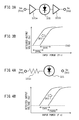
- FIGS. 3A and 3B are diagrams for explaining a modification of the receiving device.
- FIG. 3A is a block diagram of the modification of the receiving device
- FIG. 3B is a diagram for explaining the characteristic of the receiving device of FIG. 3A .
- an amplifier 101a is provided at a preceding stage of the detector 101. Even when the input power Pin of the input signal Sin is small, the input power Pin is amplified to a power which may be detected by the detector 101, and the amplified power is supplied to the detector 101.
- FIG. 3A also illustrates the case where, for example, an output signal of the detector 101 is difficult to be processed by an AD converter (102) at the subsequent stage and, in this case, an amplifier 101b is provided at the subsequent stage of the detector 101 (the preceding stage of the AD converter 102).
- the amplifier 101b is provided at the subsequent stage of the detector 101 so that, for example, even when the input power Pin is small and the output signal of the detector 101 is small, the power is amplified to a level at which the AD converter 102 at the subsequent stage may accurately perform AD conversion. Note that when the amplifier 101b is provided at the subsequent stage of the detector 101, the detected output voltage Vo is the output of the amplifier 101b.
- the dynamic range DYR simply shifts to DYRL on the low level side of the input signal (the left side in the diagram), and the dynamic range itself is difficult to be enlarged.
- FIGS. 4A and 4B are diagrams for explaining a receiving device in another modification.
- FIG. 4A is a block diagram illustrating the receiving device in another modification
- FIG. 4B is a diagram for explaining the characteristic of the receiving device of FIG. 4A .
- the receiving device in another modification is provided with an attenuator (resistor) 101c at the preceding stage of the detector 101.
- the attenuator resistor
- the power is decreased to power which may be detected by the detector 101, and the resultant power is supplied to the detector 101.
- the output signal So from the detector 101 is decreased to a level at which the AD converter 102 at the subsequent stage may accurately perform AD conversion without causing saturation.
- a resistor may be provided at the subsequent stage of the detector 101.
- the dynamic range DYR simply shifts to DYRR on the high level side of the input signal (the right side in the diagram), and the dynamic range itself is difficult to be enlarged.
- FIG. 5 is a block diagram illustrating a receiving device of a first embodiment and illustrates a receiving device to be applied to, for example, a communication device, a radar, a spectrum analyzer, or the like, for example as an AM demodulator using a diode detector.
- reference numerals 11 and 12 denote diode detectors (envelope detectors, detectors), reference numeral 2 denotes a voltmeter (or AD converter, digital circuit, or the like), 3 denotes a dividing circuit (power divider, coupler), and 4 denotes an averaging circuit.
- the receiving device includes the coupler 3 receiving the input signal Sin and dividing the signal into two divided signals Sin1 and Sin2, two detectors 11 and 12, the averaging circuit 4, and the voltmeter 2.
- the coupler 3 receives the input signal Sin and divides the input signal into the two divided signals Sin1 and Sin2 having powers different from each other in accordance with a predetermined dividing ratio.
- the coupler 3 does not equally divide the input signal Sin (1:1) but divides the input signal Sin into the two divided signals Sin1 and Sin2 so that the maximum value/minimum value, i.e., Pin1/Pin2 becomes 10, 100, 1,000, or the like.
- the input signal Sin of the input power Pin is divided to the two divided signals Sin1 and Sin2, and the ratio between the power Pin1 of the divided signal Sin1 and the power Pin2 of the divided signal Sin2 becomes 10:1.
- the input signal Sin of the input power Pin is divided to the two divided signals Sin1 and Sin2, and the ratio between the power Pin1 of the divided signal Sin1 and the power Pin2 of the divided signal Sin2 becomes 100:1.
- the input signal Sin of the input power Pin is divided to the two divided signals Sin1 and Sin2, and the ratio between the power Pin1 of the divided signal Sin1 and the power Pin2 of the divided signal Sin2 becomes 1000:1.
- the two divided signals Sin1 and Sin2 divided by the coupler 3 are supplied to the corresponding detectors 11 and 12, respectively.
- the detectors 11 and 12 have equivalent circuit configurations, equivalent characteristics, i.e., the same dynamic range.
- the coupler 3 whose dividing ratio is 10 dB is applied.
- the coupler 3 whose dividing ratio is 20 dB is applied.
- the coupler 3 whose dividing ratio is 30 dB is applied.
- the coupler 3 having a dividing ratio which is equal to or nearly equal to the dynamic range of the detectors 11 and 12. As will be specifically described later, this is because that the dynamic range of the detector 11 and that of the detector 12 may be enlarged while reducing the overlap range.
- the output signal So1 of the detector 11 and the output signal So2 of the detector 12 are supplied to the averaging circuit 4 and an averaging process is performed in the averaging circuit 4.
- An output signal of the averaging circuit 4 is supplied to the voltmeter 2 where voltage is detected.
- the voltmeter 2 may be an AD converter, a digital circuit, or the like.
- FIG. 6 is a block diagram illustrating a receiving device of a second embodiment.
- the receiving device of the second embodiment is constructed by providing an amplifier 11a between the coupler 3 and the detector 11 and providing an amplifier 12a between the coupler 3 and the detector 12.
- the amplification factors (gains) of the amplifiers 11a and 12a are equal to each other.
- the input signal Sin is divided to the two divided signals Sin1 and Sin2 by the coupler 3. Consequently, even when the power ratio between the divided signals Sin1 and Sin2 is 10:1, the power Pin1 of the divided signal Sin1 is decreased in comparison with the input power Pin.
- the amplifiers 11a and 12a are provided in order to make the general dynamic range proper.
- the amplifiers 11a and 12a are provided in the preceding stage of the detectors 11 and 12, respectively.
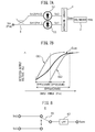
- FIGS. 7A and 7B are diagrams for explaining operation of the receiving device of the first embodiment illustrated in FIG. 5 .
- FIG. 7A corresponds to the above-described FIG. 5
- FIG. 7B is a diagram for explaining the dynamic range of a detector in the receiving device illustrated in FIG. 7A , i.e., the dynamic range of the input power Pin in the receiving device of the first embodiment.
- the detectors 11 and 12 have an equivalent circuit configuration and use, for example, the same dynamic range of 10 dB, i.e., the ratio of the upper and lower limits which may be used in the input powers Pin1 and Pin2 is 10:1.
- the coupler 3 whose dividing ratio of 10 dB is applied, and the power ratio of the input signals (the divided signals Sin1 and Sin2) of the detectors 11 and 12 divided by the coupler 3, i.e., Pin1:Pin2 is 10:1.
- a dynamic range DYRav of an output Soav of the averaging circuit 4 is, for example, obtained by adding the dynamic range DYR1 of 10 dB of the detector 11 and the dynamic range DYR2 of 10 dB of the detector 12.
- the dynamic range DYR2 of the detector 12 corresponds to, for example, DYRR in FIG. 4B described above.
- a curve CLav of the dynamic range DYRav of the receiving device is obtained by averaging a curve CL1 of DYR1 by the detector 11 and a curve CL2 of DYR2 by the detector 12 by the averaging circuit 4, so that the dynamic range DYRav is enlarged to 20 dB.
- the dividing ratio of the coupler 3 is 10 dB
- most of the input power Pin Pin1: 90%
- the detector 11 is supplied to the detector 11 and subjected to detecting process, and the output signal So1 is output.
- the curve CL1 (DYR1) of the output signal So1 is substantially same as that described with reference to FIG. 2 .
- the detector 11 is difficult to appropriately perform the detecting process.
- Pin is larger than IP1, it is saturated.
- a part (Pin2: 10%) of the input power Pin is supplied to the detector 12 and subjected to the detecting process, and the output signal So2 is output.
- the curve CL2 (DYR2) of the output signal So2 is, for example, substantially same as that described with reference to FIG. 4B .
- the detector 12 may perform the detecting process.
- the dynamic range DYRav of the receiving device is obtained by seamlessly connecting the dynamic ranges DYR1 and DYR2 of the detectors 11 and 12 and may be enlarged twice as large as the dynamic range (10 dB) of the detectors 11 and 12.
- the dynamic range DYRav of the receiving device may be enlarged to 40 dB.
- the dynamic range of the detectors 11 and 12 is 20 dB and the coupler 3 whose dividing ratio is 10 dB is applied, the dynamic ranges of the detectors 11 and 12 overlap only by 10 dB, so that the dynamic range DYRav of the receiving device becomes 30 dB.
- the dynamic range of the detectors 11 and 12 is 20 dB and the coupler 3 whose dividing ratio is 30 dB is applied, the dynamic ranges of the detectors 11 and 12 are discontinuous, so that it is not preferable.
- the dynamic range of the internal circuit may be enlarged.
- the dynamic range of the internal circuit (detector) may be enlarged, for example, the sensitivity of the detector decreases more or less due to the averaging.
- the embodiment it is preferable to apply the embodiment to a receiving device which is demanded to enlarge the dynamic range of the input power in spite of a certain amount of decrease of the sensitivity.
- a receiving device using frequency exceeding GHz band particularly, a receiving device using frequency (carrier frequency) higher than 10 GHz.
- FIG. 8 is a block diagram illustrating an example of the averaging circuit
- FIGS. 9A, 9B, 9C, and 9D are diagrams for explaining operation of a device obtained by applying the averaging circuit illustrated in FIG. 8 to the receiving device of the second embodiment illustrated in FIG. 6 .
- FIG. 9A is a block diagram of a device obtained by applying the averaging circuit 4 illustrated in FIG. 8 to the receiving device of the second embodiment
- FIG. 9B is a diagram illustrating output signals So1 and So2 of the detectors 11 and 12 and an output signal Soav of the averaging circuit 4 when a weak signal is received (when the input power Pin is weak).
- FIG. 9C is a diagram illustrating the output signals So1, So2, and Soav when the input power Pin is moderate
- FIG. 9D is a diagram illustrating the output signals So1, So2, and Soav when the input power Pin is large.
- the operations illustrated in FIGS. 9B to 9D may be applied to the receiving device of the first embodiment shown in FIG. 5 .
- the averaging circuit 4 includes a switch 41 switching between the output signals So1 and So2 of the detectors 11 and 12 at a predetermined timing and a low-pass filter 42 receiving the signal selected by the switch 41 and processing the signal.
- the low-pass filter 42 receives the output signals So1 and So2 of the detectors 11 and 12 switched at the predetermined timing by the switch 41 and performs a process of filtering high-frequency components and passing low-frequency components.
- the predetermined timing of switching the switch 41 is, for example, longer than one cycle (tin) of a carrier signal of the input signal Sin and shorter than the half of one cycle (To) of the output signals So1 and So2 of the detectors 11 and 12.
- the frequency of a switching clock of the switch 41 is sufficiently higher than that of an input signal (for example, about ten times).
- the passing frequency of the low-pass filter 42 is set so that, for example, the frequency of the switching clock of the switch 41 may be cut off.
- reference character SLd denotes a detection limit level
- SLs denotes a saturation level
- Reference numeral SLo1 denotes a detection output level of the output signal So1 of the detector 11, which corresponds to a detection output level when the switch 41 in the averaging circuit 4 selects the output signal So1 of the detector 11.
- reference numeral SLo2 denotes a detection output level of the output signal So2 of the detector 12, which corresponds to a detection output level when the switch 41 in the averaging circuit 4 selects the output signal So2 of the detector 12.
- Reference character SLoav denotes a detection output level of the output signal Soav of the averaging circuit 4, i.e., a level obtained by averaging the detection output levels SLo1 and SLo2 of the detectors 11 and 12.
- the detection output level SLo1 of the detector 11 corresponds to the input power Pin. Therefore, the average value of output signals of the detectors 11 and 12, i.e., the detection output level SLoav of the averaging circuit 4 becomes a voltage value according to the input power Pin.
- the detection output level SLoav of the averaging circuit 4 also become a voltage value according to the input power Pin.
- the detection output level SLo2 of the detector 12 becomes a voltage value according to the input power Pin. Therefore, the detection output level SLoav of the averaging circuit 4 becomes a voltage value according to the input power Pin.
- the dynamic range of the detectors 11 and 12 may be enlarged.
- FIG. 10 is a block diagram illustrating still another example of the averaging circuit.
- the averaging circuit 4 includes a differential amplifier 43 and an inverter 44.
- the differential amplifier 43 receives a signal obtained by inverting the output signal So1 output from the detector 11 (first internal circuit) by the inverter 44 and the output signal So2 output from the detector 12 (second internal circuit) by differential input terminals (+ and -) and differential-amplifies the signals.
- the differential amplifier 43 obtains the difference between the output signal So1 of the detector 11 and the output signal So2 of the detector 12 and averages the signals.
- the inverter 44 may be provided at the subsequent stage of the detector 12, invert the output signal So2 of the detector 12, and supply the resultant signal to the differential amplifier 43.
- FIG. 11 is a block diagram illustrating a receiving device of a third embodiment.
- the number of the above-described two detectors 11 and 12 is increased to N (N is an integer of two or larger).
- the receiving device of the third embodiment includes a dividing circuit 3, N pieces of detectors 11 to 1N, the averaging circuit 4, and the voltmeter (or AD converter, digital circuit, or the like).
- the N pieces of detectors 11 to 1N have equivalent circuit configurations and have the same dynamic range of, for example, 10 dB.
- the dividing circuit 3 includes N-1 pieces of dividers (power dividers, couplers) 31 to 3(N-1), and each of the couplers 31 to 3(N-1) has a dividing ratio equivalent to the dynamic range of each of the detectors 11 to 1N.
- the power Pin1 which is 90% of the input power Pin is supplied to the detector 11
- the residual power Pin2 which is 10% of the input power Pin is supplied to the detector 12.
- power PinN which is (1/10) N-1 of the input power Pin is supplied to the detector 1N.
- the detectors 11 to 1N receive corresponding divided signals Sin1 to SinN divided by the dividing circuit 3 (couplers 31 to 3(N-1)) and perform the detecting process.
- the output signals So1 to SoN of the detectors 11 to 1N are supplied to the averaging circuit 4 and subjected to the averaging process, and the resultant signal is supplied as the output signal Soav to the voltmeter 2.
- a circuit obtained by modifying the circuit in FIG. 8 may be applied. Specifically, the switch 41 switches among the output signals So1 to SoN of the N pieces of detectors 11 to 1N at a predetermined timing, and the low-pass filter 42 receives a signal selected by the switch 41 and performs a process of filtering high-frequency components and passing low-frequency components.
- the predetermined timing of switching the switch 41 is, for example, longer than one cycle (tin) of a carrier signal of the input signal Sin and shorter than 1/N of one cycle (To) of the output signals So1 to SoN of the detectors 11 to 1N.
- the switch 41 may not be switched according to the magnitude of the power of the input signal like the detectors 11, 12, ..., and 1N. In other words, it is sufficient to select output signals of all of the detectors 11 to 1N in one cycle (To) of the output signals So1 to SoN of the detectors 11 to 1N, and the order is not limited.
- the averaging circuit 4 including the differential amplifier 43 and the inverter 44 described with reference to FIG. 10 is suitable to average output signals of the two detectors 11 and 12.
- the averaging circuit 4 in FIG. 8 is preferable.
- FIG. 12 is a diagram for explaining the operation of the receiving device of the third embodiment illustrated in FIG. 11 .
- the dynamic range may be further enlarged by using N pieces (for example, N is an integer of three or larger) of detectors.
- the number of detectors which may be applied is limited.
- FIG. 13 is a block diagram illustrating a receiving device of a fourth embodiment.
- detectors are used as the internal circuits.
- mixers frequency mixers
- FIG. 13 reference numerals 51 and 52 denote mixers and 6 denotes a local oscillator (LO).
- the input signal Sin of high frequency (RF) having the input power Pin is divided by the coupler 3 into two divided signals Sin1 and Sin2 having powers different from each other in accordance with a predetermined dividing ratio of the coupler 3, and the two divided signals are supplied to respective mixers 51 and 52.
- the mixer 51 mixes the input RF signal Sin1 and a local signal from the local oscillator 6 and outputs a signal So1 of intermediate frequency (IF).
- the mixer 52 mixes the input RF signal Sin2 and a local signal from the local oscillator 6 and outputs a signal So2 of intermediate frequency.
- the output signals So1 and So2 of the mixers 51 and 52 are averaged by the averaging circuit 4 and an averaged output signal Soav is output.
- the mixers 51 and 52 also have the dynamic range for the input signal Sin (input power Pin), for example like in the detectors 11 and 12 in the foregoing embodiments, the dynamic range may be enlarged by applying the fourth embodiment.
- FIGS. 14A and 14B are diagrams for explaining the operation of a receiving device of a fifth embodiment.
- the receiving device of the fifth embodiment corresponds to a receiving device obtained by providing amplifiers 51a and 52a whose gains are equal at the preceding stage of the mixers 51 and 52 in the receiving device of the fourth embodiment illustrated in FIG. 13 .
- FIG. 14A is a block diagram of the receiving device of the fifth embodiment
- FIG. 14B is a diagram for explaining the dynamic range of the input power Pin in the receiving device of the fifth embodiment illustrated in FIG. 14A
- the mixers 51 and 52 have equivalent circuit configurations and have the same conversion loss of, for example, 10 dB (-10 dB).
- the amplifiers 51a and 52a each having the gain of 10 dB are provided at the preceding stage of the mixers 51 an 52, respectively.
- the dividing ratio of the coupler 3 is 10 dB, and the ratio between the power Pin1 of the divided signal Sin1 and the power Pin2 of the divided signal Sin2 is 10:1.
- the mixer output power according to the input power is output in a region that the input power Pin is from -30 dBm to -5 dBm.
- the dynamic range DYRm1 of the mixer 51 is 25 dB.
- the mixer 52 to which 10% of the input power Pin is supplied by the coupler 3 via the amplifier 52a outputs a mixer output power according to the input power in a region that the input power Pin is from -20 dBm to 5 dBm.
- the dynamic range DYRm2 of the mixer 52 is also 25 dB.
- the dynamic range DYRmav by the output Soav obtained by averaging the output signals So1 and So2 of the mixers 51 and 52 by the averaging circuit 4 is, for example, a region that the input power Pin is from -27 dBm to 5 dBm.
- the dynamic range DYRmav of the input power Pin which may be used, may be enlarged to 32 dB.
- FIG. 15 is a diagram schematically illustrating an example of a divider and illustrates an example of a microstrip line coupler.
- reference numeral 301 denotes a dielectric substrate
- 302 denotes an earth conductor
- 303 and 304 denote strip conductors
- 305 denotes a solder resist.
- the strip conductors 303 and 304 are formed so as to be partially parallel to each other.
- the earth conductor 302 is formed on the entire back side of the dielectric substrate 301.
- the solder resists 305 made of dielectric are formed so as to obtain a predetermined dividing ratio.
- the input signal Sin is supplied from the left side of the strip conductor 303, the divided signal Sin1 is taken out from the right side of the strip conductor 303 and, further, the divided signal Sin2 is taken out from the right side of the strip conductor 304.
- the microstrip line coupler illustrated in FIG. 15 is preferable, for example, when the application frequency (carrier frequency of the input signal Sin) is in GHz band or higher. Obviously, the microstrip line coupler illustrated in FIG. 15 is just an example, and various microstrip line couplers may be applied.
Landscapes
- Engineering & Computer Science (AREA)
- Power Engineering (AREA)
- Physics & Mathematics (AREA)
- Nonlinear Science (AREA)
- Circuits Of Receivers In General (AREA)
- Amplifiers (AREA)
Abstract
Description
- The embodiments discussed herein are related to a receiving device.
- In recent years, wireless communication technologies are applied in various fields. For example, in a demodulator of a communication device such as a cellular phone, a wireless LAN (Local Area Network), a radar, a spectrum analyzer, or the like, a receiving device which detects an input signal is used.
- For example, in a circuit (receiving device) which demodulates a signal subjected to signal amplitude modulation (AM: Amplitude Modulation), a signal received by an antenna is demodulated by an internal circuit (detector), and the demodulated signal is processed by a voltmeter, an AD (Analog-to-Digital) converter, a digital circuit, or the like. In the receiving device, for example, a range of a proper input signal intensity (input power) for operating the detector is called a dynamic range of the detector.
- For example, when the input power is smaller than the lower limit of the usable range of the detector, although the output voltage (detected voltage) of the detector is output, the voltage is too low. Therefore, for example, it is difficult to detect the voltage by a voltmeter at the subsequent stage. When input power is small, for example, an amplifier is provided at the preceding stage of the detector so that the input power becomes larger than the lower limit of the usable range of the detector.
- On the other hand, when the input power is larger than the upper limit of the usable range of the detector, an output of the detector is saturated and, for example, it becomes difficult to detect a detected voltage according to the input power by a voltmeter at the subsequent stage. Consequently, when the input power is large, for example, an attenuator (resistor) is provided at the preceding stage of the detector so that the input power becomes smaller than the upper limit of the usable range of the detector.
- As described above, the upper and lower limits of the usable range (dynamic range) exist for the input power of the detector. When the input power of the detector lies out of the dynamic range, for example, an amplifier or a resistor is provided at the preceding stage of the detector so that a process of making the input power lie in the dynamic range is performed. In some cases, an amplifier or a resistor may be provided at the subsequent stage of the detector.
- However, even when an amplifier or a resistor is provided at the preceding stage (subsequent stage) of the detector, the dynamic range itself is difficult to be enlarged. This is an issue not only for the detector but also for, for example, another internal circuit (receiving device) such as a mixer.
- Conventionally, various receiving devices with a characteristic improved by processing an input signal of a detector are being proposed.
- Patent Document 1: Japanese Laid-open Patent Publication No.
S59-133749 - Patent Document 2: Japanese Laid-open Utility Model Publication No.
S62-164410 - Patent Document 3: Japanese Laid-open Patent Publication No.
H02-078306 - Accordingly, it is an object of one aspect of the embodiments to provide a receiving device enabling to enlarge a dynamic range of the internal circuit.
- According to an aspect of the embodiments, there is provided a receiving device including a dividing circuit, N pieces of internal circuits, and an averaging circuit.
- The dividing circuit is configured to divide an input signal into N pieces of divided signals (where N is an integer of two or larger), and the N pieces of internal circuits are configured to receive and process the N pieces of divided signals. The averaging circuit is configured to receive N pieces of output signals from the N pieces of internal circuits, averaging the output signals, and output an averaged signal.
-
-
FIG. 1 is a block diagram illustrating an example of a receiving device; -
FIG. 2 is a diagram for explaining a dynamic range of a detector in the receiving device illustrated inFIG. 1 ; -
FIGS. 3A and 3B are diagrams for explaining a modification of the receiving device; -
FIGS. 4A and 4B are diagrams for explaining another modification of the receiving device; -
FIG. 5 is a block diagram illustrating a receiving device of a first embodiment; -
FIG. 6 is a block diagram illustrating a receiving device of a second embodiment; -
FIGS. 7A and 7B are diagrams for explaining operation of the receiving device of the first embodiment illustrated inFIG. 5 ; -
FIG. 8 is a block diagram illustrating an example of an averaging circuit; -
FIGS. 9A, 9B, 9C, and 9D are diagrams for explaining operation of a device obtained by applying the averaging circuit illustrated inFIG. 8 to the receiving device of the second embodiment illustrated inFIG. 6 ; -
FIG. 10 is a block diagram illustrating another example of the averaging circuit; -
FIG. 11 is a block diagram illustrating a receiving device of a third embodiment; -
FIG. 12 is a diagram for explaining the operation of the receiving device of the third embodiment illustrated inFIG. 11 ; -
FIG. 13 is a block diagram illustrating a receiving device of a fourth embodiment; -
FIGS. 14A and 14B are diagrams for explaining the operation of a receiving device of a fifth embodiment; and -
FIG. 15 is a diagram schematically illustrating an example of a divider. - Before describing embodiments of a receiving device, examples of a receiving device and their problems will be described with reference to
FIG. 1 to FIGS. 4A and4B .FIG. 1 is a block diagram illustrating an example of a receiving device and illustrates a receiving device to be applied to, for example, a communication device, a radar, a spectrum analyzer, or the like, for example as an AM demodulator using a diode detector. - In
FIG. 1 ,reference numeral 100 denotes an antenna, 101 denotes a diode detector (envelope detector, detector), and 102 denotes a voltmeter (or AD (Analog-to-Digital) converter, digital circuit, or the like). - As illustrated in
FIG. 1 , a receiving device (AM demodulator) includes thedetector 101 for receiving a reception signal (input signal) Sin from theantenna 100 and detects an envelope, and thevoltmeter 102. Thevoltmeter 102 receives a demodulation signal (output signal) So from thedetector 101, detects a voltage Vo of the signal, and outputs the voltage Vo. - In
FIG. 1 , reference character Tin denotes one cycle of a carrier wave (carrier) of the input signal Sin, and To/2 denotes a half cycle of the output signal So of thedetector 101. Therefore, one cycle of the output signal So corresponds to a cycle is about twice To/2 inFIG. 1. FIG. 2 is a diagram for explaining a dynamic range of a detector in the receiving device illustrated inFIG. 1 . InFIG. 2 , the vertical axis denotes the voltage (output of thevoltmeter 102, detected output voltage) Vo of the output signal So of thedetector 101, and the horizontal axis denotes power (input signal intensity, input power) Pin of the input signal Sin of thedetector 101. - As illustrated in
FIG. 2 , in a range where the input power Pin of thedetector 101 is from IPO to IP1, the detected output voltage Vo of thedetector 101 increases as the input power Pin increases. - However, for example, when the input power Pin of the
detector 101 is smaller than IP0, thedetector 101 is difficult to detect the input signal Sin. Alternatively, for example, when the input power Pin is smaller than IP0, even when thedetector 101 outputs an output signal, thevoltmeter 102 at the subsequent stage is difficult to detect the voltage of the output signal, and the detected output voltage Vo becomes lower than voltage DVO as the detection limit of thedetector 101. - On the other hand, for example, when the input power Pin of the
detector 101 is larger than IP1, thedetector 101 is difficult to detect the input signal Sin and the output signal So of thedetector 101 is saturated. Alternatively, when the input power Pin of thedetector 101 is larger than IP1, even when thedetector 101 outputs an output signal, thevoltmeter 102 at the subsequent stage is saturated by the output voltage. - As described above, the
detector 101 includes a predetermined range DYR specified by the upper and lower limits of the usable range in the input power (input signal) Pin, and the predetermined range DYR of the input power Pin is called a dynamic range. -
FIGS. 3A and 3B are diagrams for explaining a modification of the receiving device.FIG. 3A is a block diagram of the modification of the receiving device, andFIG. 3B is a diagram for explaining the characteristic of the receiving device ofFIG. 3A . - As illustrated in
FIG. 3A , in the modification of the receiving device, anamplifier 101a is provided at a preceding stage of thedetector 101. Even when the input power Pin of the input signal Sin is small, the input power Pin is amplified to a power which may be detected by thedetector 101, and the amplified power is supplied to thedetector 101. -
FIG. 3A also illustrates the case where, for example, an output signal of thedetector 101 is difficult to be processed by an AD converter (102) at the subsequent stage and, in this case, anamplifier 101b is provided at the subsequent stage of the detector 101 (the preceding stage of the AD converter 102). - In other words, the
amplifier 101b is provided at the subsequent stage of thedetector 101 so that, for example, even when the input power Pin is small and the output signal of thedetector 101 is small, the power is amplified to a level at which theAD converter 102 at the subsequent stage may accurately perform AD conversion. Note that when theamplifier 101b is provided at the subsequent stage of thedetector 101, the detected output voltage Vo is the output of theamplifier 101b. - However, as illustrated in
FIG. 3B , even when the amplifier is provided at the preceding stage or the subsequent stage of thedetector 101, the dynamic range DYR simply shifts to DYRL on the low level side of the input signal (the left side in the diagram), and the dynamic range itself is difficult to be enlarged. -
FIGS. 4A and 4B are diagrams for explaining a receiving device in another modification.FIG. 4A is a block diagram illustrating the receiving device in another modification, andFIG. 4B is a diagram for explaining the characteristic of the receiving device ofFIG. 4A . - As illustrated in
FIG. 4A , the receiving device in another modification is provided with an attenuator (resistor) 101c at the preceding stage of thedetector 101. For example, when the input power Pin of the input signal Sin is large, the power is decreased to power which may be detected by thedetector 101, and the resultant power is supplied to thedetector 101. - Alternatively, the output signal So from the
detector 101 is decreased to a level at which theAD converter 102 at the subsequent stage may accurately perform AD conversion without causing saturation. A resistor may be provided at the subsequent stage of thedetector 101. - However, as illustrated in
FIG. 4B , even when a resistor is provided at the preceding stage (subsequent stage) of thedetector 101, the dynamic range DYR simply shifts to DYRR on the high level side of the input signal (the right side in the diagram), and the dynamic range itself is difficult to be enlarged. - Hereinbelow, a receiving device of the embodiments will be described in detail with reference to the accompanying drawings.
FIG. 5 is a block diagram illustrating a receiving device of a first embodiment and illustrates a receiving device to be applied to, for example, a communication device, a radar, a spectrum analyzer, or the like, for example as an AM demodulator using a diode detector. - In
FIG. 5 ,reference numerals reference numeral 2 denotes a voltmeter (or AD converter, digital circuit, or the like), 3 denotes a dividing circuit (power divider, coupler), and 4 denotes an averaging circuit. - As illustrated in
FIG. 5 , the receiving device (AM demodulator) includes thecoupler 3 receiving the input signal Sin and dividing the signal into two divided signals Sin1 and Sin2, twodetectors circuit 4, and thevoltmeter 2. - The
coupler 3 receives the input signal Sin and divides the input signal into the two divided signals Sin1 and Sin2 having powers different from each other in accordance with a predetermined dividing ratio. - In other words, the
coupler 3 does not equally divide the input signal Sin (1:1) but divides the input signal Sin into the two divided signals Sin1 and Sin2 so that the maximum value/minimum value, i.e., Pin1/Pin2 becomes 10, 100, 1,000, or the like. - Concretely, for example, when the
coupler 3 having the dividing ratio of 10 dB is used, the input signal Sin of the input power Pin is divided to the two divided signals Sin1 and Sin2, and the ratio between the power Pin1 of the divided signal Sin1 and the power Pin2 of the divided signal Sin2 becomes 10:1. - For example, when the
coupler 3 having the dividing ratio of 20 dB is used, the input signal Sin of the input power Pin is divided to the two divided signals Sin1 and Sin2, and the ratio between the power Pin1 of the divided signal Sin1 and the power Pin2 of the divided signal Sin2 becomes 100:1. - Further, for example, when the
coupler 3 having the dividing ratio of 30 dB is used, the input signal Sin of the input power Pin is divided to the two divided signals Sin1 and Sin2, and the ratio between the power Pin1 of the divided signal Sin1 and the power Pin2 of the divided signal Sin2 becomes 1000:1. - As described above, the two divided signals Sin1 and Sin2 divided by the
coupler 3 are supplied to the correspondingdetectors detectors - When the dynamic range of the
detectors coupler 3 whose dividing ratio is 10 dB is applied. When the dynamic range of thedetectors coupler 3 whose dividing ratio is 20 dB is applied. Further, when the dynamic range of thedetectors coupler 3 whose dividing ratio is 30 dB is applied. - In other words, it is preferable to apply the
coupler 3 having a dividing ratio which is equal to or nearly equal to the dynamic range of thedetectors detector 11 and that of thedetector 12 may be enlarged while reducing the overlap range. - The output signal So1 of the
detector 11 and the output signal So2 of thedetector 12 are supplied to the averagingcircuit 4 and an averaging process is performed in the averagingcircuit 4. An output signal of the averagingcircuit 4 is supplied to thevoltmeter 2 where voltage is detected. Thevoltmeter 2 may be an AD converter, a digital circuit, or the like. -
FIG. 6 is a block diagram illustrating a receiving device of a second embodiment. As is clear from comparison betweenFIG. 6 and FIG. 5 described above, the receiving device of the second embodiment is constructed by providing anamplifier 11a between thecoupler 3 and thedetector 11 and providing anamplifier 12a between thecoupler 3 and thedetector 12. The amplification factors (gains) of theamplifiers - In other words, for example, in the receiving device of the first embodiment, the input signal Sin is divided to the two divided signals Sin1 and Sin2 by the
coupler 3. Consequently, even when the power ratio between the divided signals Sin1 and Sin2 is 10:1, the power Pin1 of the divided signal Sin1 is decreased in comparison with the input power Pin. - Further, since the power Pin2 of the divided signal Sin2 is significantly decreased in comparison with the input power Pin, the
amplifiers - In the receiving device of the second embodiment, the
amplifiers detectors -
FIGS. 7A and 7B are diagrams for explaining operation of the receiving device of the first embodiment illustrated inFIG. 5 .FIG. 7A corresponds to the above-describedFIG. 5 , andFIG. 7B is a diagram for explaining the dynamic range of a detector in the receiving device illustrated inFIG. 7A , i.e., the dynamic range of the input power Pin in the receiving device of the first embodiment. - It is now assumed that the
detectors - Therefore, the
coupler 3 whose dividing ratio of 10 dB is applied, and the power ratio of the input signals (the divided signals Sin1 and Sin2) of thedetectors coupler 3, i.e., Pin1:Pin2 is 10:1. - As illustrated in
FIG. 7B , a dynamic range DYRav of an output Soav of the averagingcircuit 4 is, for example, obtained by adding the dynamic range DYR1 of 10 dB of thedetector 11 and the dynamic range DYR2 of 10 dB of thedetector 12. The dynamic range DYR2 of thedetector 12 corresponds to, for example, DYRR inFIG. 4B described above. - In other words, a curve CLav of the dynamic range DYRav of the receiving device is obtained by averaging a curve CL1 of DYR1 by the
detector 11 and a curve CL2 of DYR2 by thedetector 12 by the averagingcircuit 4, so that the dynamic range DYRav is enlarged to 20 dB. - Specifically, when the dividing ratio of the
coupler 3 is 10 dB, most of the input power Pin (Pin1: 90%) is supplied to thedetector 11 and subjected to detecting process, and the output signal So1 is output. The curve CL1 (DYR1) of the output signal So1 is substantially same as that described with reference toFIG. 2 . For example, when the input power Pin is smaller than IP0, thedetector 11 is difficult to appropriately perform the detecting process. When Pin is larger than IP1, it is saturated. - A part (Pin2: 10%) of the input power Pin is supplied to the
detector 12 and subjected to the detecting process, and the output signal So2 is output. The curve CL2 (DYR2) of the output signal So2 is, for example, substantially same as that described with reference toFIG. 4B . For example, even when the input power Pin is larger than IP1, thedetector 12 may perform the detecting process. - Therefore, the dynamic range DYRav of the receiving device is obtained by seamlessly connecting the dynamic ranges DYR1 and DYR2 of the
detectors detectors - For example, when the dynamic range of the
detectors coupler 3 whose dividing ratio is 20 dB, the dynamic range DYRav of the receiving device may be enlarged to 40 dB. - When the dynamic range of the
detectors coupler 3 whose dividing ratio is 10 dB is applied, the dynamic ranges of thedetectors - However, when the dynamic range of the
detectors coupler 3 whose dividing ratio is 30 dB is applied, the dynamic ranges of thedetectors - As described above, in the receiving device of the embodiment, the dynamic range of the internal circuit may be enlarged. In the receiving device of the embodiment, although the dynamic range of the internal circuit (detector) may be enlarged, for example, the sensitivity of the detector decreases more or less due to the averaging.
- Consequently, it is preferable to apply the embodiment to a receiving device which is demanded to enlarge the dynamic range of the input power in spite of a certain amount of decrease of the sensitivity. Concretely, it is preferable to apply the embodiment to, for example, a receiving device using frequency exceeding GHz band, particularly, a receiving device using frequency (carrier frequency) higher than 10 GHz.
-
FIG. 8 is a block diagram illustrating an example of the averaging circuit, andFIGS. 9A, 9B, 9C, and 9D are diagrams for explaining operation of a device obtained by applying the averaging circuit illustrated inFIG. 8 to the receiving device of the second embodiment illustrated inFIG. 6 . -
FIG. 9A is a block diagram of a device obtained by applying the averagingcircuit 4 illustrated inFIG. 8 to the receiving device of the second embodiment, andFIG. 9B is a diagram illustrating output signals So1 and So2 of thedetectors circuit 4 when a weak signal is received (when the input power Pin is weak). -
FIG. 9C is a diagram illustrating the output signals So1, So2, and Soav when the input power Pin is moderate, andFIG. 9D is a diagram illustrating the output signals So1, So2, and Soav when the input power Pin is large. Obviously, the operations illustrated inFIGS. 9B to 9D may be applied to the receiving device of the first embodiment shown inFIG. 5 . - As illustrated in
FIGS. 8 and9A , the averagingcircuit 4 includes aswitch 41 switching between the output signals So1 and So2 of thedetectors pass filter 42 receiving the signal selected by theswitch 41 and processing the signal. - The low-
pass filter 42 receives the output signals So1 and So2 of thedetectors switch 41 and performs a process of filtering high-frequency components and passing low-frequency components. - The predetermined timing of switching the
switch 41 is, for example, longer than one cycle (tin) of a carrier signal of the input signal Sin and shorter than the half of one cycle (To) of the output signals So1 and So2 of thedetectors - In other words, the frequency of a switching clock of the
switch 41 is sufficiently higher than that of an input signal (for example, about ten times). The passing frequency of the low-pass filter 42 is set so that, for example, the frequency of the switching clock of theswitch 41 may be cut off. - Referring now to
FIGS. 9B to 9D , the relations among the magnitude of the input power Pin, the output signals So1 and So2 of thedetectors circuit 4 will be described. InFIGS. 9B to 9D , reference character SLd denotes a detection limit level, and SLs denotes a saturation level. - Reference numeral SLo1 denotes a detection output level of the output signal So1 of the
detector 11, which corresponds to a detection output level when theswitch 41 in the averagingcircuit 4 selects the output signal So1 of thedetector 11. - Further, reference numeral SLo2 denotes a detection output level of the output signal So2 of the
detector 12, which corresponds to a detection output level when theswitch 41 in the averagingcircuit 4 selects the output signal So2 of thedetector 12. Reference character SLoav denotes a detection output level of the output signal Soav of the averagingcircuit 4, i.e., a level obtained by averaging the detection output levels SLo1 and SLo2 of thedetectors - First, as illustrated in
FIG. 9B , when the input signal Sin is weak, for example, a signal smaller than the dynamic range is supplied to thedetector 12. Consequently, the detection output level SLo2 of thedetector 12 becomes a very small level which is almost equal to the detection limit level SLd. - On the other hand, for example, a signal at an operable level is supplied to the
detector 11. Consequently, the detection output level SLo1 of thedetector 11 corresponds to the input power Pin. Therefore, the average value of output signals of thedetectors circuit 4 becomes a voltage value according to the input power Pin. - Next, as illustrated in
FIG. 9C , when the input signal Sin is moderate, signals at operable levels are supplied to both of thedetectors detectors circuit 4 also become a voltage value according to the input power Pin. - Further, as illustrated in
FIG. 9D , when the input signal Sin is large, for example, a signal larger than the dynamic range is supplied to thedetector 11. Consequently, the detection output level SLo1 of thedetector 11 becomes almost the saturation level SLs. - However, since the
detector 12 is not saturated, the detection output level SLo2 of thedetector 12 becomes a voltage value according to the input power Pin. Therefore, the detection output level SLoav of the averagingcircuit 4 becomes a voltage value according to the input power Pin. - In such a manner, it is understood that, according to the receiving device of the embodiment, the dynamic range of the
detectors 11 and 12 (internal circuits) may be enlarged. -
FIG. 10 is a block diagram illustrating still another example of the averaging circuit. As illustrated inFIG. 10 , the averagingcircuit 4 includes adifferential amplifier 43 and an inverter 44. Thedifferential amplifier 43 receives a signal obtained by inverting the output signal So1 output from the detector 11 (first internal circuit) by the inverter 44 and the output signal So2 output from the detector 12 (second internal circuit) by differential input terminals (+ and -) and differential-amplifies the signals. - In other words, the
differential amplifier 43 obtains the difference between the output signal So1 of thedetector 11 and the output signal So2 of thedetector 12 and averages the signals. Obviously, the inverter 44 may be provided at the subsequent stage of thedetector 12, invert the output signal So2 of thedetector 12, and supply the resultant signal to thedifferential amplifier 43. -
FIG. 11 is a block diagram illustrating a receiving device of a third embodiment. The number of the above-described twodetectors - As illustrated in
FIG. 11 , the receiving device of the third embodiment includes adividing circuit 3, N pieces ofdetectors 11 to 1N, the averagingcircuit 4, and the voltmeter (or AD converter, digital circuit, or the like). The N pieces ofdetectors 11 to 1N have equivalent circuit configurations and have the same dynamic range of, for example, 10 dB. - The dividing
circuit 3 includes N-1 pieces of dividers (power dividers, couplers) 31 to 3(N-1), and each of thecouplers 31 to 3(N-1) has a dividing ratio equivalent to the dynamic range of each of thedetectors 11 to 1N. - Therefore, for example, the power Pin1 which is 90% of the input power Pin is supplied to the
detector 11, and the residual power Pin2 which is 10% of the input power Pin is supplied to thedetector 12. To thedetector 1N, power PinN which is (1/10)N-1 of the input power Pin is supplied. - In such a manner, the
detectors 11 to 1N receive corresponding divided signals Sin1 to SinN divided by the dividing circuit 3 (couplers 31 to 3(N-1)) and perform the detecting process. The output signals So1 to SoN of thedetectors 11 to 1N are supplied to the averagingcircuit 4 and subjected to the averaging process, and the resultant signal is supplied as the output signal Soav to thevoltmeter 2. - As the averaging
circuit 4, a circuit obtained by modifying the circuit inFIG. 8 may be applied. Specifically, theswitch 41 switches among the output signals So1 to SoN of the N pieces ofdetectors 11 to 1N at a predetermined timing, and the low-pass filter 42 receives a signal selected by theswitch 41 and performs a process of filtering high-frequency components and passing low-frequency components. - The predetermined timing of switching the
switch 41 is, for example, longer than one cycle (tin) of a carrier signal of the input signal Sin and shorter than 1/N of one cycle (To) of the output signals So1 to SoN of thedetectors 11 to 1N. - In the switching operation of the
switch 41, theswitch 41 may not be switched according to the magnitude of the power of the input signal like thedetectors detectors 11 to 1N in one cycle (To) of the output signals So1 to SoN of thedetectors 11 to 1N, and the order is not limited. - The averaging
circuit 4 including thedifferential amplifier 43 and the inverter 44 described with reference toFIG. 10 is suitable to average output signals of the twodetectors detectors 11 to 1N (N is an integer of three or larger), the averagingcircuit 4 inFIG. 8 is preferable. -
FIG. 12 is a diagram for explaining the operation of the receiving device of the third embodiment illustrated inFIG. 11 . As is clear from comparison betweenFIG. 12 andFIG. 8B described above, the dynamic range may be further enlarged by using N pieces (for example, N is an integer of three or larger) of detectors. - Obviously, due to various factors such as noise included in the input signal Sin, the characteristics of the coupler, or the characteristics of the detectors and the averaging circuit, the number of detectors which may be applied is limited.
-
FIG. 13 is a block diagram illustrating a receiving device of a fourth embodiment. In the foregoing embodiments, detectors are used as the internal circuits. In the receiving device of the fourth embodiment, mixers (frequency mixers) are applied as the internal circuit. InFIG. 13 ,reference numerals - As illustrated in
FIG. 13 , for example, the input signal Sin of high frequency (RF) having the input power Pin is divided by thecoupler 3 into two divided signals Sin1 and Sin2 having powers different from each other in accordance with a predetermined dividing ratio of thecoupler 3, and the two divided signals are supplied torespective mixers - The
mixer 51 mixes the input RF signal Sin1 and a local signal from thelocal oscillator 6 and outputs a signal So1 of intermediate frequency (IF). Similarly, themixer 52 mixes the input RF signal Sin2 and a local signal from thelocal oscillator 6 and outputs a signal So2 of intermediate frequency. - The output signals So1 and So2 of the
mixers circuit 4 and an averaged output signal Soav is output. Although themixers detectors -
FIGS. 14A and 14B are diagrams for explaining the operation of a receiving device of a fifth embodiment. The receiving device of the fifth embodiment corresponds to a receiving device obtained by providingamplifiers mixers FIG. 13 . -
FIG. 14A is a block diagram of the receiving device of the fifth embodiment, andFIG. 14B is a diagram for explaining the dynamic range of the input power Pin in the receiving device of the fifth embodiment illustrated inFIG. 14A . Themixers - As illustrated in
FIGS. 14A and 14B , theamplifiers mixers 51 an 52, respectively. The dividing ratio of thecoupler 3 is 10 dB, and the ratio between the power Pin1 of the divided signal Sin1 and the power Pin2 of the divided signal Sin2 is 10:1. - In other words, power (Pin1) of 90% of the input power Pin is led to the
amplifier 51a, and power (Pin2) of 10% of the input power Pin is led to theamplifier 52a. The gain of each of theamplifiers mixers FIG. 14B . - Concretely, as illustrated by a curve CLm1 in
FIG. 14B , in a dynamic range DYRm1 of themixer 51, for example, the mixer output power according to the input power is output in a region that the input power Pin is from -30 dBm to -5 dBm. In other words, the dynamic range DYRm1 of themixer 51 is 25 dB. - As illustrated by a curve CLm2 in
FIG. 14B , themixer 52 to which 10% of the input power Pin is supplied by thecoupler 3 via theamplifier 52a outputs a mixer output power according to the input power in a region that the input power Pin is from -20 dBm to 5 dBm. In other words, the dynamic range DYRm2 of themixer 52 is also 25 dB. - As illustrated by a curve CLmav in
FIG. 14B , the dynamic range DYRmav by the output Soav obtained by averaging the output signals So1 and So2 of themixers circuit 4 is, for example, a region that the input power Pin is from -27 dBm to 5 dBm. In other words, by the receiving device of the fifth embodiment, the dynamic range DYRmav of the input power Pin, which may be used, may be enlarged to 32 dB. -
FIG. 15 is a diagram schematically illustrating an example of a divider and illustrates an example of a microstrip line coupler. InFIG. 15 ,reference numeral 301 denotes a dielectric substrate, 302 denotes an earth conductor, 303 and 304 denote strip conductors, and 305 denotes a solder resist. - As illustrated in
FIG. 15 , on the surface of thedielectric substrate 301, thestrip conductors dielectric substrate 301, theearth conductor 302 is formed. - For example, in places of the parallel-disposed parts of the
strip conductors dielectric substrate 301, the solder resists 305 made of dielectric are formed so as to obtain a predetermined dividing ratio. - To the
coupler 3, for example, the input signal Sin is supplied from the left side of thestrip conductor 303, the divided signal Sin1 is taken out from the right side of thestrip conductor 303 and, further, the divided signal Sin2 is taken out from the right side of thestrip conductor 304. - The microstrip line coupler illustrated in
FIG. 15 is preferable, for example, when the application frequency (carrier frequency of the input signal Sin) is in GHz band or higher. Obviously, the microstrip line coupler illustrated inFIG. 15 is just an example, and various microstrip line couplers may be applied.
Claims (15)
- A receiving device comprising:a dividing circuit configured to divide an input signal into N pieces of divided signals (where N is an integer of two or larger);N pieces of internal circuits configured to receive and process the N pieces of divided signals; andan averaging circuit configured to receive N pieces of output signals from the N pieces of internal circuits, averaging the output signals, and output an averaged signal.
- The receiving device according to claim 1, wherein the dividing circuit divides the input signal into the N pieces of divided signals so that the divided signals have powers different from each other.
- The receiving device according to claim 2, wherein the dividing circuit includes N-1 pieces of dividers, and
each of the dividers divides a dividing-target signal which is supplied into two divided signals having powers different from each other in accordance with a predetermined dividing ratio. - The receiving device according to claim 3, wherein when N is an integer of three or larger, the divider in the (N-1)th stage receives, as the dividing-target signal, one of two divided signals divided from the divider in the (N-2)th stage.
- The receiving device according to claim 3 or 4, wherein the N pieces of internal circuits are equivalent circuits each other, and
the predetermined dividing ratio is equal to a dynamic range of each of the internal circuits. - The receiving device according to any one of claims 3 to 5, wherein each of the dividers is a microstrip line divider.
- The receiving device according to any one of claims 1 to 6, wherein the averaging circuit comprises:a switch switching among the N pieces of output signals; anda low-pass filter receiving a signal selected by the switch, filtering high-frequency components, and passing low-frequency components.
- The receiving device according to claim 7, wherein the switch is switched at a timing shorter than 1/N of one cycle in the N pieces of output signal and longer than one cycle of a carrier signal of the input signal.
- The receiving device according to claim 8, wherein the low-pass filter cuts off frequency of a switching clock used for switch-control on the switch.
- The receiving device according to any one of claims 1 to 9, wherein the N pieces of internal circuits are two internal circuits which are first and second internal circuits.
- The receiving device according to claim 10, wherein the averaging circuit includes a differential amplifier and an inverter, and
the differential amplifier receives, through differential input terminals, a signal obtained by inverting a first output signal which is output from the first internal circuit by the inverter and a second output signal which is output from the second internal circuit. - The receiving device according to any one of claims 1 to 11, the receiving device further comprising N pieces of amplifiers provided at the preceding stages of the N pieces of internal circuits.
- The receiving device according to any one of claims 1 to 12, wherein each of the internal circuits is a detector.
- The receiving device according to any one of claims 1 to 12, wherein each of the internal circuits is a mixer.
- The receiving device according to any one of claims 1 to 14, wherein the input signal is a signal of 10 GHz or higher.
Applications Claiming Priority (1)
| Application Number | Priority Date | Filing Date | Title |
|---|---|---|---|
| JP2013040621A JP6175805B2 (en) | 2013-03-01 | 2013-03-01 | Receiver |
Publications (2)
| Publication Number | Publication Date |
|---|---|
| EP2773038A1 true EP2773038A1 (en) | 2014-09-03 |
| EP2773038B1 EP2773038B1 (en) | 2017-09-13 |
Family
ID=50002551
Family Applications (1)
| Application Number | Title | Priority Date | Filing Date |
|---|---|---|---|
| EP14152448.8A Not-in-force EP2773038B1 (en) | 2013-03-01 | 2014-01-24 | Receiving device |
Country Status (3)
| Country | Link |
|---|---|
| US (1) | US9490748B2 (en) |
| EP (1) | EP2773038B1 (en) |
| JP (1) | JP6175805B2 (en) |
Citations (4)
| Publication number | Priority date | Publication date | Assignee | Title |
|---|---|---|---|---|
| JPS59133749A (en) | 1983-01-21 | 1984-08-01 | Fujitsu Ltd | Radio communication system |
| JPS62164410U (en) | 1986-04-08 | 1987-10-19 | ||
| JPH0278306A (en) | 1988-09-14 | 1990-03-19 | Nec Corp | Phase detection circuit |
| US7619468B1 (en) * | 2008-09-30 | 2009-11-17 | Nortel Networks Limited | Doherty amplifier with drain bias supply modulation |
Family Cites Families (11)
| Publication number | Priority date | Publication date | Assignee | Title |
|---|---|---|---|---|
| JPS61207128A (en) * | 1985-03-07 | 1986-09-13 | 三菱電機株式会社 | Anti-time limiting relay |
| JPH03125506A (en) * | 1989-10-11 | 1991-05-28 | Furuno Electric Co Ltd | Dynamic range magnification device for detection circuit |
| JPH05114294A (en) * | 1991-10-22 | 1993-05-07 | Mitsubishi Electric Corp | Synapse expressing circuit and semiconductor neural network device |
| JP3828879B2 (en) * | 2003-05-23 | 2006-10-04 | 松下電器産業株式会社 | Detection circuit |
| KR100605587B1 (en) * | 2005-03-31 | 2006-07-28 | 주식회사 하이닉스반도체 | Semiconductor memory device that can adjust the driving force of output driver internally |
| KR20070024342A (en) * | 2005-08-25 | 2007-03-02 | 엘지.필립스 엘시디 주식회사 | Data voltage generating circuit and generating method |
| JP2007235804A (en) * | 2006-03-03 | 2007-09-13 | Matsushita Electric Ind Co Ltd | Reception field strength detection circuit and reception field strength detection method |
| JP4821639B2 (en) * | 2007-02-09 | 2011-11-24 | 富士通株式会社 | Amplitude detector |
| US7760013B2 (en) * | 2008-02-06 | 2010-07-20 | Analog Devices, Inc. | Transadmittance and filter having a gain function |
| JP5741579B2 (en) * | 2010-06-22 | 2015-07-01 | 日本電気株式会社 | Power detection circuit |
| JP2012227809A (en) * | 2011-04-21 | 2012-11-15 | Nec Corp | Detection circuit and detection method |
-
2013
- 2013-03-01 JP JP2013040621A patent/JP6175805B2/en not_active Expired - Fee Related
-
2014
- 2014-01-24 EP EP14152448.8A patent/EP2773038B1/en not_active Not-in-force
- 2014-01-27 US US14/164,390 patent/US9490748B2/en not_active Expired - Fee Related
Patent Citations (5)
| Publication number | Priority date | Publication date | Assignee | Title |
|---|---|---|---|---|
| JPS59133749A (en) | 1983-01-21 | 1984-08-01 | Fujitsu Ltd | Radio communication system |
| EP0115385A2 (en) * | 1983-01-21 | 1984-08-08 | Fujitsu Limited | Radio communication system |
| JPS62164410U (en) | 1986-04-08 | 1987-10-19 | ||
| JPH0278306A (en) | 1988-09-14 | 1990-03-19 | Nec Corp | Phase detection circuit |
| US7619468B1 (en) * | 2008-09-30 | 2009-11-17 | Nortel Networks Limited | Doherty amplifier with drain bias supply modulation |
Also Published As
| Publication number | Publication date |
|---|---|
| US9490748B2 (en) | 2016-11-08 |
| JP6175805B2 (en) | 2017-08-09 |
| JP2014171006A (en) | 2014-09-18 |
| EP2773038B1 (en) | 2017-09-13 |
| US20140247083A1 (en) | 2014-09-04 |
Similar Documents
| Publication | Publication Date | Title |
|---|---|---|
| US8351490B2 (en) | Radio frequency identification transceiver | |
| US7873342B2 (en) | Low IF receiver of rejecting image signal and image signal rejection method | |
| KR20000075616A (en) | Receiver if system with active filters | |
| US6356746B1 (en) | Direct converting receiver | |
| CN101257465A (en) | Signal conversion method, quadrature demodulator and zero-IF receiver | |
| US8736249B2 (en) | High frequency power detector circuit and radio communication device | |
| EP2688214A1 (en) | Gain control circuit, communication apparatus, electronic device, and gain control method | |
| US10425071B2 (en) | Fast settling peak detector | |
| Ahmed et al. | A SiGe-based wideband 220–310-GHz subharmonic receiver front-end for high resolution radar applications | |
| EP2773038B1 (en) | Receiving device | |
| El-Shennawy et al. | A dual band FMCW radar receiver with integrated active balun and baseband AGC loop | |
| US6987957B2 (en) | Dual-band frequency converter unit with high operability | |
| CN110764061B (en) | Orthogonal frequency conversion receiver | |
| US9148103B2 (en) | Gain measurement circuit, gain measurement method, and communication apparatus | |
| Tran et al. | Design of a front-end for satellite receiver | |
| CN215641523U (en) | Novel millimeter wave large dynamic high linear logarithm detector | |
| CN215575356U (en) | Frequency spectrograph system with Tuner chip | |
| JP2009231883A (en) | Radio receiver | |
| CN115668816B (en) | Wireless receiving circuit | |
| Zhang et al. | An e band wideband superheterodyne receiver front-end using large-dynamic-range automatic-gain-control loop | |
| US7511557B2 (en) | Quadrature mixer circuit and RF communication semiconductor integrated circuit | |
| CN108183876B (en) | FSK signal demodulation and pulse recovery system and method | |
| CN223207110U (en) | Frequency conversion module under high stray bandwidth of 18GHz ~40GHz | |
| Chi et al. | A 60-GHz wireless transceiver with dual-mode power amplifier for IEEE 802.11 ad in 65nm CMOS | |
| Ha et al. | A 3-5GHz IR-UWB CMOS RF transceiver with RF notch filter |
Legal Events
| Date | Code | Title | Description |
|---|---|---|---|
| PUAI | Public reference made under article 153(3) epc to a published international application that has entered the european phase |
Free format text: ORIGINAL CODE: 0009012 |
|
| 17P | Request for examination filed |
Effective date: 20140124 |
|
| AK | Designated contracting states |
Kind code of ref document: A1 Designated state(s): AL AT BE BG CH CY CZ DE DK EE ES FI FR GB GR HR HU IE IS IT LI LT LU LV MC MK MT NL NO PL PT RO RS SE SI SK SM TR |
|
| AX | Request for extension of the european patent |
Extension state: BA ME |
|
| R17P | Request for examination filed (corrected) |
Effective date: 20140811 |
|
| RBV | Designated contracting states (corrected) |
Designated state(s): AL AT BE BG CH CY CZ DE DK EE ES FI FR GB GR HR HU IE IS IT LI LT LU LV MC MK MT NL NO PL PT RO RS SE SI SK SM TR |
|
| GRAP | Despatch of communication of intention to grant a patent |
Free format text: ORIGINAL CODE: EPIDOSNIGR1 |
|
| INTG | Intention to grant announced |
Effective date: 20170406 |
|
| GRAS | Grant fee paid |
Free format text: ORIGINAL CODE: EPIDOSNIGR3 |
|
| GRAA | (expected) grant |
Free format text: ORIGINAL CODE: 0009210 |
|
| AK | Designated contracting states |
Kind code of ref document: B1 Designated state(s): AL AT BE BG CH CY CZ DE DK EE ES FI FR GB GR HR HU IE IS IT LI LT LU LV MC MK MT NL NO PL PT RO RS SE SI SK SM TR |
|
| REG | Reference to a national code |
Ref country code: GB Ref legal event code: FG4D |
|
| REG | Reference to a national code |
Ref country code: CH Ref legal event code: EP |
|
| REG | Reference to a national code |
Ref country code: IE Ref legal event code: FG4D |
|
| REG | Reference to a national code |
Ref country code: AT Ref legal event code: REF Ref document number: 929073 Country of ref document: AT Kind code of ref document: T Effective date: 20171015 |
|
| REG | Reference to a national code |
Ref country code: DE Ref legal event code: R096 Ref document number: 602014014424 Country of ref document: DE |
|
| REG | Reference to a national code |
Ref country code: FR Ref legal event code: PLFP Year of fee payment: 5 |
|
| REG | Reference to a national code |
Ref country code: NL Ref legal event code: MP Effective date: 20170913 |
|
| REG | Reference to a national code |
Ref country code: LT Ref legal event code: MG4D |
|
| PG25 | Lapsed in a contracting state [announced via postgrant information from national office to epo] |
Ref country code: HR Free format text: LAPSE BECAUSE OF FAILURE TO SUBMIT A TRANSLATION OF THE DESCRIPTION OR TO PAY THE FEE WITHIN THE PRESCRIBED TIME-LIMIT Effective date: 20170913 Ref country code: SE Free format text: LAPSE BECAUSE OF FAILURE TO SUBMIT A TRANSLATION OF THE DESCRIPTION OR TO PAY THE FEE WITHIN THE PRESCRIBED TIME-LIMIT Effective date: 20170913 Ref country code: LT Free format text: LAPSE BECAUSE OF FAILURE TO SUBMIT A TRANSLATION OF THE DESCRIPTION OR TO PAY THE FEE WITHIN THE PRESCRIBED TIME-LIMIT Effective date: 20170913 Ref country code: NO Free format text: LAPSE BECAUSE OF FAILURE TO SUBMIT A TRANSLATION OF THE DESCRIPTION OR TO PAY THE FEE WITHIN THE PRESCRIBED TIME-LIMIT Effective date: 20171213 Ref country code: FI Free format text: LAPSE BECAUSE OF FAILURE TO SUBMIT A TRANSLATION OF THE DESCRIPTION OR TO PAY THE FEE WITHIN THE PRESCRIBED TIME-LIMIT Effective date: 20170913 |
|
| REG | Reference to a national code |
Ref country code: AT Ref legal event code: MK05 Ref document number: 929073 Country of ref document: AT Kind code of ref document: T Effective date: 20170913 |
|
| PG25 | Lapsed in a contracting state [announced via postgrant information from national office to epo] |
Ref country code: GR Free format text: LAPSE BECAUSE OF FAILURE TO SUBMIT A TRANSLATION OF THE DESCRIPTION OR TO PAY THE FEE WITHIN THE PRESCRIBED TIME-LIMIT Effective date: 20171214 Ref country code: BG Free format text: LAPSE BECAUSE OF FAILURE TO SUBMIT A TRANSLATION OF THE DESCRIPTION OR TO PAY THE FEE WITHIN THE PRESCRIBED TIME-LIMIT Effective date: 20171213 Ref country code: ES Free format text: LAPSE BECAUSE OF FAILURE TO SUBMIT A TRANSLATION OF THE DESCRIPTION OR TO PAY THE FEE WITHIN THE PRESCRIBED TIME-LIMIT Effective date: 20170913 Ref country code: RS Free format text: LAPSE BECAUSE OF FAILURE TO SUBMIT A TRANSLATION OF THE DESCRIPTION OR TO PAY THE FEE WITHIN THE PRESCRIBED TIME-LIMIT Effective date: 20170913 Ref country code: LV Free format text: LAPSE BECAUSE OF FAILURE TO SUBMIT A TRANSLATION OF THE DESCRIPTION OR TO PAY THE FEE WITHIN THE PRESCRIBED TIME-LIMIT Effective date: 20170913 |
|
| PG25 | Lapsed in a contracting state [announced via postgrant information from national office to epo] |
Ref country code: NL Free format text: LAPSE BECAUSE OF FAILURE TO SUBMIT A TRANSLATION OF THE DESCRIPTION OR TO PAY THE FEE WITHIN THE PRESCRIBED TIME-LIMIT Effective date: 20170913 |
|
| PG25 | Lapsed in a contracting state [announced via postgrant information from national office to epo] |
Ref country code: CZ Free format text: LAPSE BECAUSE OF FAILURE TO SUBMIT A TRANSLATION OF THE DESCRIPTION OR TO PAY THE FEE WITHIN THE PRESCRIBED TIME-LIMIT Effective date: 20170913 Ref country code: RO Free format text: LAPSE BECAUSE OF FAILURE TO SUBMIT A TRANSLATION OF THE DESCRIPTION OR TO PAY THE FEE WITHIN THE PRESCRIBED TIME-LIMIT Effective date: 20170913 Ref country code: PL Free format text: LAPSE BECAUSE OF FAILURE TO SUBMIT A TRANSLATION OF THE DESCRIPTION OR TO PAY THE FEE WITHIN THE PRESCRIBED TIME-LIMIT Effective date: 20170913 |
|
| PG25 | Lapsed in a contracting state [announced via postgrant information from national office to epo] |
Ref country code: EE Free format text: LAPSE BECAUSE OF FAILURE TO SUBMIT A TRANSLATION OF THE DESCRIPTION OR TO PAY THE FEE WITHIN THE PRESCRIBED TIME-LIMIT Effective date: 20170913 Ref country code: SK Free format text: LAPSE BECAUSE OF FAILURE TO SUBMIT A TRANSLATION OF THE DESCRIPTION OR TO PAY THE FEE WITHIN THE PRESCRIBED TIME-LIMIT Effective date: 20170913 Ref country code: AT Free format text: LAPSE BECAUSE OF FAILURE TO SUBMIT A TRANSLATION OF THE DESCRIPTION OR TO PAY THE FEE WITHIN THE PRESCRIBED TIME-LIMIT Effective date: 20170913 Ref country code: SM Free format text: LAPSE BECAUSE OF FAILURE TO SUBMIT A TRANSLATION OF THE DESCRIPTION OR TO PAY THE FEE WITHIN THE PRESCRIBED TIME-LIMIT Effective date: 20170913 Ref country code: IS Free format text: LAPSE BECAUSE OF FAILURE TO SUBMIT A TRANSLATION OF THE DESCRIPTION OR TO PAY THE FEE WITHIN THE PRESCRIBED TIME-LIMIT Effective date: 20180113 Ref country code: IT Free format text: LAPSE BECAUSE OF FAILURE TO SUBMIT A TRANSLATION OF THE DESCRIPTION OR TO PAY THE FEE WITHIN THE PRESCRIBED TIME-LIMIT Effective date: 20170913 |
|
| REG | Reference to a national code |
Ref country code: DE Ref legal event code: R097 Ref document number: 602014014424 Country of ref document: DE |
|
| PLBE | No opposition filed within time limit |
Free format text: ORIGINAL CODE: 0009261 |
|
| STAA | Information on the status of an ep patent application or granted ep patent |
Free format text: STATUS: NO OPPOSITION FILED WITHIN TIME LIMIT |
|
| PG25 | Lapsed in a contracting state [announced via postgrant information from national office to epo] |
Ref country code: DK Free format text: LAPSE BECAUSE OF FAILURE TO SUBMIT A TRANSLATION OF THE DESCRIPTION OR TO PAY THE FEE WITHIN THE PRESCRIBED TIME-LIMIT Effective date: 20170913 |
|
| 26N | No opposition filed |
Effective date: 20180614 |
|
| REG | Reference to a national code |
Ref country code: CH Ref legal event code: PL |
|
| PG25 | Lapsed in a contracting state [announced via postgrant information from national office to epo] |
Ref country code: LU Free format text: LAPSE BECAUSE OF NON-PAYMENT OF DUE FEES Effective date: 20180124 |
|
| REG | Reference to a national code |
Ref country code: IE Ref legal event code: MM4A |
|
| REG | Reference to a national code |
Ref country code: BE Ref legal event code: MM Effective date: 20180131 |
|
| PG25 | Lapsed in a contracting state [announced via postgrant information from national office to epo] |
Ref country code: LI Free format text: LAPSE BECAUSE OF NON-PAYMENT OF DUE FEES Effective date: 20180131 Ref country code: CH Free format text: LAPSE BECAUSE OF NON-PAYMENT OF DUE FEES Effective date: 20180131 Ref country code: BE Free format text: LAPSE BECAUSE OF NON-PAYMENT OF DUE FEES Effective date: 20180131 Ref country code: SI Free format text: LAPSE BECAUSE OF FAILURE TO SUBMIT A TRANSLATION OF THE DESCRIPTION OR TO PAY THE FEE WITHIN THE PRESCRIBED TIME-LIMIT Effective date: 20170913 |
|
| PG25 | Lapsed in a contracting state [announced via postgrant information from national office to epo] |
Ref country code: IE Free format text: LAPSE BECAUSE OF NON-PAYMENT OF DUE FEES Effective date: 20180124 |
|
| PG25 | Lapsed in a contracting state [announced via postgrant information from national office to epo] |
Ref country code: MC Free format text: LAPSE BECAUSE OF FAILURE TO SUBMIT A TRANSLATION OF THE DESCRIPTION OR TO PAY THE FEE WITHIN THE PRESCRIBED TIME-LIMIT Effective date: 20170913 |
|
| PG25 | Lapsed in a contracting state [announced via postgrant information from national office to epo] |
Ref country code: MT Free format text: LAPSE BECAUSE OF NON-PAYMENT OF DUE FEES Effective date: 20180124 |
|
| PG25 | Lapsed in a contracting state [announced via postgrant information from national office to epo] |
Ref country code: TR Free format text: LAPSE BECAUSE OF FAILURE TO SUBMIT A TRANSLATION OF THE DESCRIPTION OR TO PAY THE FEE WITHIN THE PRESCRIBED TIME-LIMIT Effective date: 20170913 |
|
| PG25 | Lapsed in a contracting state [announced via postgrant information from national office to epo] |
Ref country code: HU Free format text: LAPSE BECAUSE OF FAILURE TO SUBMIT A TRANSLATION OF THE DESCRIPTION OR TO PAY THE FEE WITHIN THE PRESCRIBED TIME-LIMIT; INVALID AB INITIO Effective date: 20140124 Ref country code: PT Free format text: LAPSE BECAUSE OF FAILURE TO SUBMIT A TRANSLATION OF THE DESCRIPTION OR TO PAY THE FEE WITHIN THE PRESCRIBED TIME-LIMIT Effective date: 20170913 |
|
| PG25 | Lapsed in a contracting state [announced via postgrant information from national office to epo] |
Ref country code: CY Free format text: LAPSE BECAUSE OF FAILURE TO SUBMIT A TRANSLATION OF THE DESCRIPTION OR TO PAY THE FEE WITHIN THE PRESCRIBED TIME-LIMIT Effective date: 20170913 Ref country code: MK Free format text: LAPSE BECAUSE OF NON-PAYMENT OF DUE FEES Effective date: 20170913 |
|
| PG25 | Lapsed in a contracting state [announced via postgrant information from national office to epo] |
Ref country code: AL Free format text: LAPSE BECAUSE OF FAILURE TO SUBMIT A TRANSLATION OF THE DESCRIPTION OR TO PAY THE FEE WITHIN THE PRESCRIBED TIME-LIMIT Effective date: 20170913 |
|
| REG | Reference to a national code |
Ref country code: DE Ref legal event code: R082 Ref document number: 602014014424 Country of ref document: DE Representative=s name: HL KEMPNER PATENTANWAELTE, SOLICITORS (ENGLAND, DE Ref country code: DE Ref legal event code: R082 Ref document number: 602014014424 Country of ref document: DE Representative=s name: HL KEMPNER PATENTANWALT, RECHTSANWALT, SOLICIT, DE |
|
| PGFP | Annual fee paid to national office [announced via postgrant information from national office to epo] |
Ref country code: GB Payment date: 20221201 Year of fee payment: 10 Ref country code: FR Payment date: 20221208 Year of fee payment: 10 |
|
| PGFP | Annual fee paid to national office [announced via postgrant information from national office to epo] |
Ref country code: DE Payment date: 20221130 Year of fee payment: 10 |
|
| REG | Reference to a national code |
Ref country code: DE Ref legal event code: R119 Ref document number: 602014014424 Country of ref document: DE |
|
| GBPC | Gb: european patent ceased through non-payment of renewal fee |
Effective date: 20240124 |
|
| PG25 | Lapsed in a contracting state [announced via postgrant information from national office to epo] |
Ref country code: DE Free format text: LAPSE BECAUSE OF NON-PAYMENT OF DUE FEES Effective date: 20240801 |
|
| PG25 | Lapsed in a contracting state [announced via postgrant information from national office to epo] |
Ref country code: GB Free format text: LAPSE BECAUSE OF NON-PAYMENT OF DUE FEES Effective date: 20240124 |
|
| PG25 | Lapsed in a contracting state [announced via postgrant information from national office to epo] |
Ref country code: FR Free format text: LAPSE BECAUSE OF NON-PAYMENT OF DUE FEES Effective date: 20240131 |
|
| PG25 | Lapsed in a contracting state [announced via postgrant information from national office to epo] |
Ref country code: GB Free format text: LAPSE BECAUSE OF NON-PAYMENT OF DUE FEES Effective date: 20240124 Ref country code: FR Free format text: LAPSE BECAUSE OF NON-PAYMENT OF DUE FEES Effective date: 20240131 Ref country code: DE Free format text: LAPSE BECAUSE OF NON-PAYMENT OF DUE FEES Effective date: 20240801 |