EP2773013A1 - Charging circuit and charger - Google Patents
Charging circuit and charger Download PDFInfo
- Publication number
- EP2773013A1 EP2773013A1 EP13738047.3A EP13738047A EP2773013A1 EP 2773013 A1 EP2773013 A1 EP 2773013A1 EP 13738047 A EP13738047 A EP 13738047A EP 2773013 A1 EP2773013 A1 EP 2773013A1
- Authority
- EP
- European Patent Office
- Prior art keywords
- charging
- temperature
- product
- charged
- charger
- Prior art date
- Legal status (The legal status is an assumption and is not a legal conclusion. Google has not performed a legal analysis and makes no representation as to the accuracy of the status listed.)
- Granted
Links
- 238000001514 detection method Methods 0.000 claims abstract description 37
- 230000002708 enhancing effect Effects 0.000 abstract description 3
- 238000010586 diagram Methods 0.000 description 2
- 125000004122 cyclic group Chemical group 0.000 description 1
- 230000004048 modification Effects 0.000 description 1
- 238000012986 modification Methods 0.000 description 1
Images
Classifications
-
- H—ELECTRICITY
- H01—ELECTRIC ELEMENTS
- H01M—PROCESSES OR MEANS, e.g. BATTERIES, FOR THE DIRECT CONVERSION OF CHEMICAL ENERGY INTO ELECTRICAL ENERGY
- H01M10/00—Secondary cells; Manufacture thereof
- H01M10/42—Methods or arrangements for servicing or maintenance of secondary cells or secondary half-cells
- H01M10/44—Methods for charging or discharging
- H01M10/443—Methods for charging or discharging in response to temperature
-
- H—ELECTRICITY
- H01—ELECTRIC ELEMENTS
- H01M—PROCESSES OR MEANS, e.g. BATTERIES, FOR THE DIRECT CONVERSION OF CHEMICAL ENERGY INTO ELECTRICAL ENERGY
- H01M10/00—Secondary cells; Manufacture thereof
- H01M10/42—Methods or arrangements for servicing or maintenance of secondary cells or secondary half-cells
- H01M10/48—Accumulators combined with arrangements for measuring, testing or indicating the condition of cells, e.g. the level or density of the electrolyte
- H01M10/486—Accumulators combined with arrangements for measuring, testing or indicating the condition of cells, e.g. the level or density of the electrolyte for measuring temperature
-
- H—ELECTRICITY
- H02—GENERATION; CONVERSION OR DISTRIBUTION OF ELECTRIC POWER
- H02J—CIRCUIT ARRANGEMENTS OR SYSTEMS FOR SUPPLYING OR DISTRIBUTING ELECTRIC POWER; SYSTEMS FOR STORING ELECTRIC ENERGY
- H02J7/00—Circuit arrangements for charging or depolarising batteries or for supplying loads from batteries
- H02J7/0029—Circuit arrangements for charging or depolarising batteries or for supplying loads from batteries with safety or protection devices or circuits
- H02J7/00309—Overheat or overtemperature protection
-
- H—ELECTRICITY
- H02—GENERATION; CONVERSION OR DISTRIBUTION OF ELECTRIC POWER
- H02J—CIRCUIT ARRANGEMENTS OR SYSTEMS FOR SUPPLYING OR DISTRIBUTING ELECTRIC POWER; SYSTEMS FOR STORING ELECTRIC ENERGY
- H02J7/00—Circuit arrangements for charging or depolarising batteries or for supplying loads from batteries
- H02J7/007—Regulation of charging or discharging current or voltage
- H02J7/007188—Regulation of charging or discharging current or voltage the charge cycle being controlled or terminated in response to non-electric parameters
- H02J7/007192—Regulation of charging or discharging current or voltage the charge cycle being controlled or terminated in response to non-electric parameters in response to temperature
-
- H—ELECTRICITY
- H02—GENERATION; CONVERSION OR DISTRIBUTION OF ELECTRIC POWER
- H02J—CIRCUIT ARRANGEMENTS OR SYSTEMS FOR SUPPLYING OR DISTRIBUTING ELECTRIC POWER; SYSTEMS FOR STORING ELECTRIC ENERGY
- H02J7/00—Circuit arrangements for charging or depolarising batteries or for supplying loads from batteries
- H02J7/02—Circuit arrangements for charging or depolarising batteries or for supplying loads from batteries for charging batteries from ac mains by converters
- H02J7/04—Regulation of charging current or voltage
-
- Y—GENERAL TAGGING OF NEW TECHNOLOGICAL DEVELOPMENTS; GENERAL TAGGING OF CROSS-SECTIONAL TECHNOLOGIES SPANNING OVER SEVERAL SECTIONS OF THE IPC; TECHNICAL SUBJECTS COVERED BY FORMER USPC CROSS-REFERENCE ART COLLECTIONS [XRACs] AND DIGESTS
- Y02—TECHNOLOGIES OR APPLICATIONS FOR MITIGATION OR ADAPTATION AGAINST CLIMATE CHANGE
- Y02E—REDUCTION OF GREENHOUSE GAS [GHG] EMISSIONS, RELATED TO ENERGY GENERATION, TRANSMISSION OR DISTRIBUTION
- Y02E60/00—Enabling technologies; Technologies with a potential or indirect contribution to GHG emissions mitigation
- Y02E60/10—Energy storage using batteries
Definitions
- the present invention relates to the field of charging circuits, and in particular, to a charging circuit and a charger.
- chargers for charging the electronic terminals are also widely used.
- an existing charger provides overvoltage protection or over-current protection during charging.
- An objective of embodiments of the present invention is to provide a charging circuit to resolve a problem that a thermal safety accident may be caused by considerable heat generated by a product being charged or a charger because of an excessively high charging current during charging.
- An embodiment of the present invention is implemented as follows: a charging circuit, where the charging circuit includes:
- Another objective of the embodiments of the present invention is to provide a charger, where the charger includes a charging circuit, and the charging circuit includes:
- a charging circuit adjusts magnitude of a charging current according to a temperature of a product being charged or a charger, and then controls the temperature of the product being charged or the charger, thereby greatly improving user experience, and enhancing safety performance of the product with a heat protection function.
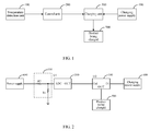
- FIG. 1 illustrates a module structure of a charging circuit according to an embodiment of the present invention. For ease of description, only a part related to this embodiment of the present invention is illustrated.
- the charging circuit includes:
- FIG. 2 illustrates a circuit structure of the charging circuit according to the embodiments of the present invention. For ease of description, only a part related to the embodiments of the present invention is illustrated.
- the temperature detection unit 100 includes:
- the power supply 600 is a power supply terminal of a board power manager (PMU) or a charger.
- PMU board power manager
- control unit 200 includes a main processing chip U1, where a detection terminal ADC of the main processing chip U1 connects to the common connection terminal between the voltage divider resistor R2 and the thermistor R1, and an output terminal OUT of the main processing chip U1 connects to the charging unit 300.
- the charging unit 300 includes a charging chip U2, where an input terminal IN of the charging chip U2 connects to the charging power supply 400, a control terminal Ctrl of the charging chip U2 connects to the output terminal OUT of the main processing chip U1, and an output terminal OUT of the charging chip U2 connects to the product 500 being charged.
- the thermistor R1 is located on a board in a superheated area of the charger's housing or a board in a superheated area of a housing of the product 500 being charged.
- An embodiment of the present invention further provides a charger, where the charger includes a charging circuit.
- the charging circuit includes:
- the temperature detection unit 100 includes:
- the power supply 600 is a power supply terminal of a board power manager (PMU) or the charger.
- PMU board power manager
- control unit 200 includes a main processing chip U1, where a detection terminal ADC of the main processing chip U1 connects to the common connection terminal between the voltage divider resistor R2 and the thermistor R1, and an output terminal OUT of the main processing chip U1 connects to the charging unit 300.
- the charging unit 300 includes a charging chip U2, where an input terminal IN of the charging chip U2 connects to the charging power supply 400, a control terminal Ctrl of the charging chip U2 connects to the output terminal OUT of the main processing chip U1, and an output terminal OUT of the charging chip U2 connects to the product 500 being charged.
- the thermistor R1 is located on a board in a superheated area of the charger's housing or a board in a superheated area of a housing of the product 500 being charged.
- An operating principle of a charging circuit is as follows:
- the main processing chip U1 controls the charging chip U2 so as to increase the charging current, thereby quickening a charging speed.
- a cyclic control may achieve an objective of both ensuring a charging speed and improving thermal experience of a user (or thermal safety of the product).
- a charging circuit with heat protection adjusts magnitude of a charging current according to a temperature of a product being charged or a charger, and then controls the temperature of the product being charged or the charger, thereby greatly improving user experience, and enhancing safety performance of the product with the heat protection function.
Abstract
Description
- The present invention relates to the field of charging circuits, and in particular, to a charging circuit and a charger.
- Nowadays, with widespread use of electronic terminals, chargers for charging the electronic terminals are also widely used. In general, an existing charger provides overvoltage protection or over-current protection during charging.
- However, when a user charges the electronic terminal such as a mobile phone, a product being charged or the charger may generate considerable heat because of an excessively high charging current. This affects user experience and the heat may even lead to a thermal safety accident.
- An objective of embodiments of the present invention is to provide a charging circuit to resolve a problem that a thermal safety accident may be caused by considerable heat generated by a product being charged or a charger because of an excessively high charging current during charging.
- An embodiment of the present invention is implemented as follows: a charging circuit, where the charging circuit includes:
- a temperature detection unit, configured to detect a temperature of a product being charged or a charger and generate detection temperature information;
- a charging unit, disposed between a charging power supply and the product being charged, and configured to provide a charging current for the product being charged; and
- a control unit, separately connected to the temperature detection unit and the charging unit, and configured to: separately compare the temperature detection information with a preset temperature upper limit and a preset temperature lower limit, control the charging unit so as to reduce the charging current when the temperature of the product being charged or the charger reaches the temperature upper limit, and control the charging unit so as to increase the charging current when the temperature of the product being charged or the charger reaches the temperature lower limit.
- Another objective of the embodiments of the present invention is to provide a charger, where the charger includes a charging circuit, and the charging circuit includes:
- a temperature detection unit, configured to detect a temperature of a product being charged or the charger and generate detection temperature information;
- a charging unit, disposed between a charging power supply and the product being charged, and configured to provide a charging current for the product being charged; and
- a control unit, separately connected to the temperature detection unit and the charging unit, and configured to: separately compare the temperature detection information with a preset temperature upper limit and a preset temperature lower limit, control the charging unit so as to reduce the charging current when the temperature of the product being charged or the charger reaches the temperature upper limit, and control the charging unit so as to increase the charging current when the temperature of the product being charged or the charger reaches the temperature lower limit.
- In the embodiments of the present invention, a charging circuit adjusts magnitude of a charging current according to a temperature of a product being charged or a charger, and then controls the temperature of the product being charged or the charger, thereby greatly improving user experience, and enhancing safety performance of the product with a heat protection function.
-
-
FIG. 1 is a module structural diagram of a charging circuit according to an embodiment of the present invention; and -
FIG. 2 is a circuit structural diagram of a charging circuit according to an embodiment of the present invention. - To make the objectives, technical solutions, and advantages of the present invention clearer and more comprehensible, the following further describes the present invention in detail with reference to the accompanying drawings and embodiments. It should be understood that the specific embodiments described herein are merely used to explain the present invention but are not intended to limit the present invention.
FIG. 1 illustrates a module structure of a charging circuit according to an embodiment of the present invention. For ease of description, only a part related to this embodiment of the present invention is illustrated. - The charging circuit includes:
- a
temperature detection unit 100, configured to detect a temperature of aproduct 500 being charged or a charger and generate detection temperature information; - a
charging unit 300, disposed between acharging power supply 400 and theproduct 500 being charged, and configured to provide a charging current for theproduct 500 being charged; and - a
control unit 200, separately connected to thetemperature detection unit 100 and thecharging unit 300, and configured to: separately compare the temperature detection information with a preset temperature upper limit and a preset temperature lower limit, control thecharging unit 300 so as to reduce the charging current when the temperature of theproduct 500 being charged or the charger reaches the temperature upper limit, and control thecharging unit 300 so as to increase the charging current when the temperature of theproduct 500 being charged or the charger reaches the temperature lower limit. -
FIG. 2 illustrates a circuit structure of the charging circuit according to the embodiments of the present invention. For ease of description, only a part related to the embodiments of the present invention is illustrated. - In one embodiment of the present invention, the
temperature detection unit 100 includes: - a thermistor R1 and a voltage divider resistor R2, where:
- a first terminal of the voltage divider resistor R2 connects to a
power supply 600, a second terminal of the voltage divider resistor R2 is grounded by using the thermistor R1, and a common connection terminal between the voltage divider resistor R2 and the thermistor R1 connects to thecontrol unit 200.
- a first terminal of the voltage divider resistor R2 connects to a
- The
power supply 600 is a power supply terminal of a board power manager (PMU) or a charger. - In one embodiment of the present invention, the
control unit 200 includes a main processing chip U1, where a detection terminal ADC of the main processing chip U1 connects to the common connection terminal between the voltage divider resistor R2 and the thermistor R1, and an output terminal OUT of the main processing chip U1 connects to thecharging unit 300. - In one embodiment of the present invention, the
charging unit 300 includes a charging chip U2, where an input terminal IN of the charging chip U2 connects to thecharging power supply 400, a control terminal Ctrl of the charging chip U2 connects to the output terminal OUT of the main processing chip U1, and an output terminal OUT of the charging chip U2 connects to theproduct 500 being charged. - In one embodiment of the present invention, the thermistor R1 is located on a board in a superheated area of the charger's housing or a board in a superheated area of a housing of the
product 500 being charged. - An embodiment of the present invention further provides a charger, where the charger includes a charging circuit. As shown in
FIG. 1 , the charging circuit includes: - a
temperature detection unit 100, configured to detect a temperature of aproduct 500 being charged or the charger and generate detection temperature information; - a
charging unit 300, disposed between acharging power supply 400 and theproduct 500 being charged, and configured to provide a charging current for theproduct 500 being charged; and - a
control unit 200, separately connected to thetemperature detection unit 100 and thecharging unit 300, and configured to: separately compare the temperature detection information with a preset temperature upper limit and a preset temperature lower limit, control thecharging unit 300 so as to reduce the charging current when the temperature of theproduct 500 being charged or the charger reaches the temperature upper limit, and control thecharging unit 300 so as to increase the charging current when the temperature of theproduct 500 being charged or the charger reaches the temperature lower limit. - As shown in
FIG. 2 , in one embodiment of the present invention, thetemperature detection unit 100 includes: - a thermistor R1 and a voltage divider resistor R2, where:
- a first terminal of the voltage divider resistor R2 connects to a
power supply 600, a second terminal of the voltage divider resistor R2 is grounded by using the thermistor R1, and a common connection terminal between the voltage divider resistor R2 and the thermistor R1 connects to thecontrol unit 200.
- a first terminal of the voltage divider resistor R2 connects to a
- The
power supply 600 is a power supply terminal of a board power manager (PMU) or the charger. - In one embodiment of the present invention, the
control unit 200 includes a main processing chip U1, where a detection terminal ADC of the main processing chip U1 connects to the common connection terminal between the voltage divider resistor R2 and the thermistor R1, and an output terminal OUT of the main processing chip U1 connects to thecharging unit 300. - In one embodiment of the present invention, the
charging unit 300 includes a charging chip U2, where an input terminal IN of the charging chip U2 connects to thecharging power supply 400, a control terminal Ctrl of the charging chip U2 connects to the output terminal OUT of the main processing chip U1, and an output terminal OUT of the charging chip U2 connects to theproduct 500 being charged. - In one embodiment of the present invention, the thermistor R1 is located on a board in a superheated area of the charger's housing or a board in a superheated area of a housing of the
product 500 being charged. - An operating principle of a charging circuit is as follows:
- First, a thermistor R1 is installed on a board in a superheated area of a charger's housing or on a board in a superheated area of a housing of a product being charged, where the thermistor R1 is configured to detect a temperature of the charger or a
product 500 being charged; power is supplied to the thermistor R1 via a voltage divider resistor R2 and by using a power supply terminal of a board power manager (PMU) or the charger to form a temperature detection circuit. A main processing chip U1 obtains detection temperature information detected by the thermistor R1 by using a detection terminal ADC, the main processing chip U1 sets a temperature upper limit and a temperature lower limit in advance by using software, and compares the temperature detection information with the preset temperature upper limit and the preset temperature lower limit; when the temperature of theproduct 500 being charged or the charger reaches the temperature upper limit, the main processing chip U1 outputs a control signal from an output terminal OUT, and controls a charging chip U2 so as to reduce a charging current for theproduct 500 being charged, thereby reducing heat consumption during charging and achieving an objective of reducing the temperature of the charger or theproduct 500 being charged. - With adjustment of the charging current, when the temperature of the
product 500 being charged or the charger reaches the temperature lower limit, the main processing chip U1 controls the charging chip U2 so as to increase the charging current, thereby quickening a charging speed. In this way, a cyclic control may achieve an objective of both ensuring a charging speed and improving thermal experience of a user (or thermal safety of the product). - In the embodiments of the present invention, a charging circuit with heat protection adjusts magnitude of a charging current according to a temperature of a product being charged or a charger, and then controls the temperature of the product being charged or the charger, thereby greatly improving user experience, and enhancing safety performance of the product with the heat protection function.
- The foregoing descriptions are merely exemplary embodiments of the present invention, but are not intended to limit the present invention. Any modification, equivalent replacement, or improvement made without departing from the spirit and principle of the present invention should fall within the protection scope of the present invention.
Claims (10)
- A charging circuit, wherein the charging circuit comprises:a temperature detection unit, configured to detect a temperature of a product being charged or a charger and generate detection temperature information;a charging unit, disposed between a charging power supply and the product being charged, and configured to provide a charging current for the product being charged; anda control unit, separately connected to the temperature detection unit and the charging unit, and configured to: separately compare the temperature detection information with a preset temperature upper limit and a preset temperature lower limit, control the charging unit so as to reduce the charging current when the temperature of the product being charged or the charger reaches the temperature upper limit, and control the charging unit so as to increase the charging current when the temperature of the product being charged or the charger reaches the temperature lower limit.
- The charging circuit according to claim 1, wherein the temperature detection unit comprises:a thermistor R1 and a voltage divider resistor R2, wherein:a first terminal of the voltage divider resistor R2 connects to a power supply, a second terminal of the voltage divider resistor R2 is grounded by using the thermistor R1, and a common connection terminal between the voltage divider resistor R2 and the thermistor R1 connects to the control unit.
- The charging circuit according to claim 2, wherein the control unit comprises a main processing chip U1, wherein a detection terminal ADC of the main processing chip U1 connects to the common connection terminal between the voltage divider resistor R2 and the thermistor R1, and an output terminal OUT of the main processing chip U1 connects to the charging unit.
- The charging circuit according to claim 3, wherein the charging unit comprises a charging chip U2, wherein an input terminal IN of the charging chip U2 connects to the charging power supply, a control terminal Ctrl of the charging chip U2 connects to the output terminal OUT of the main processing chip U1, and an output terminal OUT of the charging chip U2 connects to the product being charged.
- The charging circuit according to claim 2, wherein the thermistor R1 is located on a board in a superheated area of the charger's housing or a board in a superheated area of a housing of the product being charged.
- A charger, wherein the charger comprises a charging circuit, and the charging circuit comprises:a temperature detection unit, configured to detect a temperature of a product being charged or the charger and generate detection temperature information;a charging unit, disposed between a charging power supply and the product being charged, and configured to provide a charging current for the product being charged; anda control unit, separately connected to the temperature detection unit and the charging unit, and configured to: separately compare the temperature detection information with a preset temperature upper limit and a preset temperature lower limit, control the charging unit so as to reduce the charging current when the temperature of the product being charged or the charger reaches the temperature upper limit, and control the charging unit so as to increase the charging current when the temperature of the product being charged or the charger reaches the temperature lower limit.
- The charger according to claim 6, wherein the temperature detection unit comprises:a thermistor R1 and a voltage divider resistor R2, wherein:a first terminal of the voltage divider resistor R2 connects to a power supply, a second terminal of the voltage divider resistor R2 is grounded by using the thermistor R1, and a common connection terminal between the voltage divider resistor R2 and the thermistor R1 connects to the control unit.
- The charger according to claim 7, wherein the control unit comprises a main processing chip U1, wherein a detection terminal ADC of the main processing chip U1 connects to the common connection terminal between the voltage divider resistor R2 and the thermistor R1, and an output terminal OUT of the main processing chip U1 connects to the charging unit.
- The charger according to claim 8, wherein the charging unit comprises a charging chip U2, wherein an input terminal IN of the charging chip U2 connects to the charging power supply, a control terminal Ctrl of the charging chip U2 connects to the output terminal OUT of the main processing chip U1, and an output terminal OUT of the charging chip U2 connects to the product being charged.
- The charger according to claim 7, wherein the thermistor R1 is located on a board in a superheated area of the charger's housing or a board in a superheated area of a housing of the product being charged.
Applications Claiming Priority (2)
| Application Number | Priority Date | Filing Date | Title |
|---|---|---|---|
| CN201210013672.7A CN103208824B (en) | 2012-01-16 | 2012-01-16 | A kind of charging circuit and charger |
| PCT/CN2013/070091 WO2013107303A1 (en) | 2012-01-16 | 2013-01-06 | Charging circuit and charger |
Publications (3)
| Publication Number | Publication Date |
|---|---|
| EP2773013A1 true EP2773013A1 (en) | 2014-09-03 |
| EP2773013A4 EP2773013A4 (en) | 2015-07-15 |
| EP2773013B1 EP2773013B1 (en) | 2019-04-03 |
Family
ID=48755951
Family Applications (1)
| Application Number | Title | Priority Date | Filing Date |
|---|---|---|---|
| EP13738047.3A Active EP2773013B1 (en) | 2012-01-16 | 2013-01-06 | Charging circuit and charger |
Country Status (5)
| Country | Link |
|---|---|
| US (1) | US20140266016A1 (en) |
| EP (1) | EP2773013B1 (en) |
| JP (1) | JP2015507457A (en) |
| CN (1) | CN103208824B (en) |
| WO (1) | WO2013107303A1 (en) |
Cited By (1)
| Publication number | Priority date | Publication date | Assignee | Title |
|---|---|---|---|---|
| CN106598105A (en) * | 2016-12-22 | 2017-04-26 | 上海与德信息技术有限公司 | Temperature control circuit and temperature control method based on mobile terminal |
Families Citing this family (22)
| Publication number | Priority date | Publication date | Assignee | Title |
|---|---|---|---|---|
| CN104348196B (en) * | 2013-07-29 | 2018-07-13 | 华为终端有限公司 | A kind of mobile communication terminal and its external charging method |
| CN104377660B (en) * | 2013-08-13 | 2019-11-26 | 中兴通讯股份有限公司 | A kind of mobile terminal charging temperature guard method and device |
| CN104638712B (en) * | 2013-11-15 | 2018-10-16 | 维沃移动通信有限公司 | A kind of mobile handsets for preventing USB socket from being overheated in charging process and method |
| CN104718739B (en) * | 2013-12-31 | 2018-09-07 | 华为终端有限公司 | Adjusting method, the apparatus and system of voltage are carried on a kind of phone |
| CN104795847A (en) * | 2014-01-22 | 2015-07-22 | 华为终端有限公司 | Power supply method, power supply device and terminal device |
| JP6264162B2 (en) * | 2014-04-04 | 2018-01-24 | 株式会社村田製作所 | Charging device, charging control method, power storage device, power storage device, power system, and electric vehicle |
| CN105846486A (en) * | 2015-06-30 | 2016-08-10 | 维沃移动通信有限公司 | Method and device for adjusting heating value of charging circuit |
| CN105140986A (en) * | 2015-08-26 | 2015-12-09 | 苏州市博得立电源科技有限公司 | Temperature detection based charging protection device of charger |
| CN105071501A (en) * | 2015-09-08 | 2015-11-18 | 上海传英信息技术有限公司 | Large-current fast charging system with temperature control function and charging method of large-current fast charging system |
| KR101734704B1 (en) * | 2015-11-05 | 2017-05-11 | 한양대학교 산학협력단 | Method for charging battery and battery charger using temperature detection |
| CN105356543A (en) * | 2015-11-25 | 2016-02-24 | Tcl移动通信科技(宁波)有限公司 | Charging current setting and processing method and system for mobile terminal |
| CN107240937A (en) * | 2016-03-28 | 2017-10-10 | 中兴通讯股份有限公司 | The charging method and device of a kind of ferric phosphate lithium cell |
| CN106100054B (en) * | 2016-07-25 | 2019-08-23 | 沈阳工程学院 | The efficiency-timed circuit of charge and discharge |
| CN106208315B (en) * | 2016-07-25 | 2019-08-23 | 沈阳工程学院 | The efficiency-timed power supply system of charge and discharge |
| CN106450533A (en) * | 2016-09-21 | 2017-02-22 | 奇酷互联网络科技(深圳)有限公司 | Charging method, charging device and terminal equipment |
| CN107959314A (en) * | 2016-10-17 | 2018-04-24 | 中兴通讯股份有限公司 | A kind of trickle charge method for electrically and intelligent terminal |
| CN107037839A (en) * | 2016-11-11 | 2017-08-11 | 上海与德信息技术有限公司 | A kind of mobile device temperature-control circuit |
| CN106712192A (en) * | 2017-01-11 | 2017-05-24 | 上海传英信息技术有限公司 | Charging method for mobile terminal |
| CN108429304B (en) * | 2018-02-27 | 2021-04-27 | 漳州科华技术有限责任公司 | Charging current control method and device, computer device and readable storage medium |
| CN111293736B (en) * | 2018-12-07 | 2023-11-03 | 青岛海信移动通信技术有限公司 | Method and equipment for controlling temperature |
| CN113036247A (en) * | 2021-04-30 | 2021-06-25 | 哈尔滨工业大学 | Quick charging method for alkali metal battery |
| CN113840362B (en) | 2021-11-26 | 2022-03-04 | 华中科技大学 | Mobile phone terminal optimization method based on energy consumption interruption probability |
Family Cites Families (18)
| Publication number | Priority date | Publication date | Assignee | Title |
|---|---|---|---|---|
| US6075342A (en) * | 1989-12-05 | 2000-06-13 | Intermec Ip Corp. | Fast battery charging system and method |
| JPH0714261B2 (en) * | 1988-11-19 | 1995-02-15 | 松下電工株式会社 | Charger |
| US5623195A (en) * | 1994-06-22 | 1997-04-22 | Lucent Technologies Inc. | Apparatus and method for controlling a charging voltage of a battery based on battery temperature |
| JP3509382B2 (en) * | 1995-04-27 | 2004-03-22 | 日産自動車株式会社 | Charge control system |
| CN1118916C (en) * | 1999-10-18 | 2003-08-20 | 神基科技股份有限公司 | Charge control device and method |
| JP2001145274A (en) * | 1999-11-15 | 2001-05-25 | Matsushita Electric Ind Co Ltd | Portable device including a charger |
| CN1153052C (en) * | 1999-11-16 | 2004-06-09 | 威盛电子股份有限公司 | Method and device for testing temp. of notebook computer |
| JP2005065476A (en) * | 2003-07-25 | 2005-03-10 | Sanyo Electric Co Ltd | Method for charging battery |
| JP2006271136A (en) * | 2005-03-24 | 2006-10-05 | Denso Corp | Dc-dc converter device |
| JP2006288150A (en) * | 2005-04-04 | 2006-10-19 | Hitachi Koki Co Ltd | Charging device for lithium battery |
| JP2008067426A (en) * | 2006-09-04 | 2008-03-21 | Yamaha Motor Electronics Co Ltd | Vehicular charge control method |
| JP2009017703A (en) * | 2007-07-05 | 2009-01-22 | Mitsumi Electric Co Ltd | Charge control circuit of secondary battery and charge control device using the circuit |
| JP4660523B2 (en) * | 2007-09-19 | 2011-03-30 | レノボ・シンガポール・プライベート・リミテッド | Charging system that controls charging at the surface temperature of the battery cell |
| JP5363740B2 (en) * | 2008-01-31 | 2013-12-11 | パナソニック株式会社 | Charge control circuit, battery pack, and charging system |
| JP4692554B2 (en) * | 2008-02-06 | 2011-06-01 | ソニー株式会社 | Charger |
| JP5309641B2 (en) * | 2008-03-24 | 2013-10-09 | ミツミ電機株式会社 | Semiconductor integrated circuit for charge control |
| JP2009268345A (en) * | 2008-04-01 | 2009-11-12 | Panasonic Corp | Charging equipment for secondary-battery pack |
| CN201584763U (en) * | 2009-12-04 | 2010-09-15 | 上海复鑫电源科技有限公司 | Intelligent charger with temperature sensor |
-
2012
- 2012-01-16 CN CN201210013672.7A patent/CN103208824B/en active Active
-
2013
- 2013-01-06 JP JP2014546304A patent/JP2015507457A/en active Pending
- 2013-01-06 EP EP13738047.3A patent/EP2773013B1/en active Active
- 2013-01-06 WO PCT/CN2013/070091 patent/WO2013107303A1/en active Application Filing
-
2014
- 2014-05-30 US US14/291,530 patent/US20140266016A1/en not_active Abandoned
Cited By (1)
| Publication number | Priority date | Publication date | Assignee | Title |
|---|---|---|---|---|
| CN106598105A (en) * | 2016-12-22 | 2017-04-26 | 上海与德信息技术有限公司 | Temperature control circuit and temperature control method based on mobile terminal |
Also Published As
| Publication number | Publication date |
|---|---|
| EP2773013B1 (en) | 2019-04-03 |
| US20140266016A1 (en) | 2014-09-18 |
| JP2015507457A (en) | 2015-03-05 |
| CN103208824A (en) | 2013-07-17 |
| EP2773013A4 (en) | 2015-07-15 |
| WO2013107303A1 (en) | 2013-07-25 |
| CN103208824B (en) | 2016-12-07 |
Similar Documents
| Publication | Publication Date | Title |
|---|---|---|
| EP2773013A1 (en) | Charging circuit and charger | |
| US9906061B2 (en) | Quick charging mobile terminal, method and system | |
| JP5791007B2 (en) | Power supply apparatus and method, and user apparatus | |
| US9268381B2 (en) | Terminal device and power supply method for terminal device | |
| EP3098931B1 (en) | Charging circuit and terminal | |
| US8368359B2 (en) | Power management unit for portable electronic devices | |
| EP2991156B1 (en) | Method and device for performing large-current charging on intelligent terminal | |
| US20150236522A1 (en) | Usb charging system with variable charging voltage, charger and smart terminal | |
| US8654493B2 (en) | Protection circuit and input/output circuit | |
| US8324867B2 (en) | Protection structure for battery charging | |
| US20130257356A1 (en) | Electronic device having charging current setting unit and charging method | |
| CN105337374A (en) | Method for prolonging power supply time | |
| JP2012182987A (en) | Electronic apparatus | |
| CN102738765B (en) | Circuit protection device and protection method | |
| US20140253016A1 (en) | Mobile power supply device and power supply system thereof | |
| US9420657B2 (en) | Flat panel electronic device and current control system thereof | |
| CN105098871A (en) | Portable device and method for controlling charging current thereof | |
| CN104753034B (en) | Electronic device and its charge protector | |
| CN106058798B (en) | Voltage protection, method and wearable device | |
| CN103246336A (en) | Electronic apparatus and driving control method thereof | |
| US10312701B2 (en) | Charging method and portable electronic device using the same | |
| WO2016188301A1 (en) | Charging detection circuit, mobile terminal and charging detection system | |
| WO2017201735A1 (en) | Battery protecting board, battery, and mobile terminal | |
| CN203798986U (en) | Automatic detection device for lithium battery | |
| CN102412610B (en) | Linear-charging circuit and intelligent charging method thereof |
Legal Events
| Date | Code | Title | Description |
|---|---|---|---|
| PUAI | Public reference made under article 153(3) epc to a published international application that has entered the european phase |
Free format text: ORIGINAL CODE: 0009012 |
|
| 17P | Request for examination filed |
Effective date: 20140528 |
|
| AK | Designated contracting states |
Kind code of ref document: A1 Designated state(s): AL AT BE BG CH CY CZ DE DK EE ES FI FR GB GR HR HU IE IS IT LI LT LU LV MC MK MT NL NO PL PT RO RS SE SI SK SM TR |
|
| DAX | Request for extension of the european patent (deleted) | ||
| RA4 | Supplementary search report drawn up and despatched (corrected) |
Effective date: 20150612 |
|
| RIC1 | Information provided on ipc code assigned before grant |
Ipc: H01M 10/44 20060101ALI20150608BHEP Ipc: H02J 7/04 20060101ALI20150608BHEP Ipc: H02J 7/00 20060101AFI20150608BHEP |
|
| 17Q | First examination report despatched |
Effective date: 20160321 |
|
| RAP1 | Party data changed (applicant data changed or rights of an application transferred) |
Owner name: HUAWEI DEVICE (DONGGUAN) CO., LTD. |
|
| REG | Reference to a national code |
Ref country code: DE Ref legal event code: R079 Ref document number: 602013053293 Country of ref document: DE Free format text: PREVIOUS MAIN CLASS: H02J0007000000 Ipc: H01M0010480000 |
|
| RIC1 | Information provided on ipc code assigned before grant |
Ipc: H02J 7/00 20060101ALI20180823BHEP Ipc: H01M 10/48 20060101AFI20180823BHEP |
|
| GRAP | Despatch of communication of intention to grant a patent |
Free format text: ORIGINAL CODE: EPIDOSNIGR1 |
|
| STAA | Information on the status of an ep patent application or granted ep patent |
Free format text: STATUS: GRANT OF PATENT IS INTENDED |
|
| INTG | Intention to grant announced |
Effective date: 20181024 |
|
| GRAS | Grant fee paid |
Free format text: ORIGINAL CODE: EPIDOSNIGR3 |
|
| GRAA | (expected) grant |
Free format text: ORIGINAL CODE: 0009210 |
|
| STAA | Information on the status of an ep patent application or granted ep patent |
Free format text: STATUS: THE PATENT HAS BEEN GRANTED |
|
| AK | Designated contracting states |
Kind code of ref document: B1 Designated state(s): AL AT BE BG CH CY CZ DE DK EE ES FI FR GB GR HR HU IE IS IT LI LT LU LV MC MK MT NL NO PL PT RO RS SE SI SK SM TR |
|
| REG | Reference to a national code |
Ref country code: GB Ref legal event code: FG4D |
|
| REG | Reference to a national code |
Ref country code: CH Ref legal event code: EP Ref country code: AT Ref legal event code: REF Ref document number: 1116884 Country of ref document: AT Kind code of ref document: T Effective date: 20190415 |
|
| REG | Reference to a national code |
Ref country code: DE Ref legal event code: R096 Ref document number: 602013053293 Country of ref document: DE |
|
| REG | Reference to a national code |
Ref country code: IE Ref legal event code: FG4D |
|
| RAP2 | Party data changed (patent owner data changed or rights of a patent transferred) |
Owner name: HUAWEI DEVICE CO., LTD. |
|
| REG | Reference to a national code |
Ref country code: NL Ref legal event code: HC Owner name: HUAWEI DEVICE CO., LTD.; CN Free format text: DETAILS ASSIGNMENT: CHANGE OF OWNER(S), CHANGE OF OWNER(S) NAME; FORMER OWNER NAME: HUAWEI DEVICE (DONGGUAN) CO., LTD. Effective date: 20190514 |
|
| REG | Reference to a national code |
Ref country code: NL Ref legal event code: FP |
|
| REG | Reference to a national code |
Ref country code: LT Ref legal event code: MG4D |
|
| REG | Reference to a national code |
Ref country code: AT Ref legal event code: MK05 Ref document number: 1116884 Country of ref document: AT Kind code of ref document: T Effective date: 20190403 |
|
| PG25 | Lapsed in a contracting state [announced via postgrant information from national office to epo] |
Ref country code: NO Free format text: LAPSE BECAUSE OF FAILURE TO SUBMIT A TRANSLATION OF THE DESCRIPTION OR TO PAY THE FEE WITHIN THE PRESCRIBED TIME-LIMIT Effective date: 20190703 Ref country code: HR Free format text: LAPSE BECAUSE OF FAILURE TO SUBMIT A TRANSLATION OF THE DESCRIPTION OR TO PAY THE FEE WITHIN THE PRESCRIBED TIME-LIMIT Effective date: 20190403 Ref country code: CZ Free format text: LAPSE BECAUSE OF FAILURE TO SUBMIT A TRANSLATION OF THE DESCRIPTION OR TO PAY THE FEE WITHIN THE PRESCRIBED TIME-LIMIT Effective date: 20190403 Ref country code: LT Free format text: LAPSE BECAUSE OF FAILURE TO SUBMIT A TRANSLATION OF THE DESCRIPTION OR TO PAY THE FEE WITHIN THE PRESCRIBED TIME-LIMIT Effective date: 20190403 Ref country code: ES Free format text: LAPSE BECAUSE OF FAILURE TO SUBMIT A TRANSLATION OF THE DESCRIPTION OR TO PAY THE FEE WITHIN THE PRESCRIBED TIME-LIMIT Effective date: 20190403 Ref country code: AL Free format text: LAPSE BECAUSE OF FAILURE TO SUBMIT A TRANSLATION OF THE DESCRIPTION OR TO PAY THE FEE WITHIN THE PRESCRIBED TIME-LIMIT Effective date: 20190403 Ref country code: PT Free format text: LAPSE BECAUSE OF FAILURE TO SUBMIT A TRANSLATION OF THE DESCRIPTION OR TO PAY THE FEE WITHIN THE PRESCRIBED TIME-LIMIT Effective date: 20190803 Ref country code: SE Free format text: LAPSE BECAUSE OF FAILURE TO SUBMIT A TRANSLATION OF THE DESCRIPTION OR TO PAY THE FEE WITHIN THE PRESCRIBED TIME-LIMIT Effective date: 20190403 Ref country code: FI Free format text: LAPSE BECAUSE OF FAILURE TO SUBMIT A TRANSLATION OF THE DESCRIPTION OR TO PAY THE FEE WITHIN THE PRESCRIBED TIME-LIMIT Effective date: 20190403 |
|
| PG25 | Lapsed in a contracting state [announced via postgrant information from national office to epo] |
Ref country code: LV Free format text: LAPSE BECAUSE OF FAILURE TO SUBMIT A TRANSLATION OF THE DESCRIPTION OR TO PAY THE FEE WITHIN THE PRESCRIBED TIME-LIMIT Effective date: 20190403 Ref country code: GR Free format text: LAPSE BECAUSE OF FAILURE TO SUBMIT A TRANSLATION OF THE DESCRIPTION OR TO PAY THE FEE WITHIN THE PRESCRIBED TIME-LIMIT Effective date: 20190704 Ref country code: RS Free format text: LAPSE BECAUSE OF FAILURE TO SUBMIT A TRANSLATION OF THE DESCRIPTION OR TO PAY THE FEE WITHIN THE PRESCRIBED TIME-LIMIT Effective date: 20190403 Ref country code: PL Free format text: LAPSE BECAUSE OF FAILURE TO SUBMIT A TRANSLATION OF THE DESCRIPTION OR TO PAY THE FEE WITHIN THE PRESCRIBED TIME-LIMIT Effective date: 20190403 Ref country code: BG Free format text: LAPSE BECAUSE OF FAILURE TO SUBMIT A TRANSLATION OF THE DESCRIPTION OR TO PAY THE FEE WITHIN THE PRESCRIBED TIME-LIMIT Effective date: 20190703 |
|
| PG25 | Lapsed in a contracting state [announced via postgrant information from national office to epo] |
Ref country code: AT Free format text: LAPSE BECAUSE OF FAILURE TO SUBMIT A TRANSLATION OF THE DESCRIPTION OR TO PAY THE FEE WITHIN THE PRESCRIBED TIME-LIMIT Effective date: 20190403 Ref country code: IS Free format text: LAPSE BECAUSE OF FAILURE TO SUBMIT A TRANSLATION OF THE DESCRIPTION OR TO PAY THE FEE WITHIN THE PRESCRIBED TIME-LIMIT Effective date: 20190803 |
|
| REG | Reference to a national code |
Ref country code: DE Ref legal event code: R097 Ref document number: 602013053293 Country of ref document: DE |
|
| PG25 | Lapsed in a contracting state [announced via postgrant information from national office to epo] |
Ref country code: SK Free format text: LAPSE BECAUSE OF FAILURE TO SUBMIT A TRANSLATION OF THE DESCRIPTION OR TO PAY THE FEE WITHIN THE PRESCRIBED TIME-LIMIT Effective date: 20190403 Ref country code: RO Free format text: LAPSE BECAUSE OF FAILURE TO SUBMIT A TRANSLATION OF THE DESCRIPTION OR TO PAY THE FEE WITHIN THE PRESCRIBED TIME-LIMIT Effective date: 20190403 Ref country code: EE Free format text: LAPSE BECAUSE OF FAILURE TO SUBMIT A TRANSLATION OF THE DESCRIPTION OR TO PAY THE FEE WITHIN THE PRESCRIBED TIME-LIMIT Effective date: 20190403 Ref country code: DK Free format text: LAPSE BECAUSE OF FAILURE TO SUBMIT A TRANSLATION OF THE DESCRIPTION OR TO PAY THE FEE WITHIN THE PRESCRIBED TIME-LIMIT Effective date: 20190403 |
|
| PLBE | No opposition filed within time limit |
Free format text: ORIGINAL CODE: 0009261 |
|
| STAA | Information on the status of an ep patent application or granted ep patent |
Free format text: STATUS: NO OPPOSITION FILED WITHIN TIME LIMIT |
|
| PG25 | Lapsed in a contracting state [announced via postgrant information from national office to epo] |
Ref country code: SM Free format text: LAPSE BECAUSE OF FAILURE TO SUBMIT A TRANSLATION OF THE DESCRIPTION OR TO PAY THE FEE WITHIN THE PRESCRIBED TIME-LIMIT Effective date: 20190403 Ref country code: IT Free format text: LAPSE BECAUSE OF FAILURE TO SUBMIT A TRANSLATION OF THE DESCRIPTION OR TO PAY THE FEE WITHIN THE PRESCRIBED TIME-LIMIT Effective date: 20190403 |
|
| 26N | No opposition filed |
Effective date: 20200106 |
|
| PG25 | Lapsed in a contracting state [announced via postgrant information from national office to epo] |
Ref country code: TR Free format text: LAPSE BECAUSE OF FAILURE TO SUBMIT A TRANSLATION OF THE DESCRIPTION OR TO PAY THE FEE WITHIN THE PRESCRIBED TIME-LIMIT Effective date: 20190403 |
|
| PG25 | Lapsed in a contracting state [announced via postgrant information from national office to epo] |
Ref country code: SI Free format text: LAPSE BECAUSE OF FAILURE TO SUBMIT A TRANSLATION OF THE DESCRIPTION OR TO PAY THE FEE WITHIN THE PRESCRIBED TIME-LIMIT Effective date: 20190403 |
|
| PG25 | Lapsed in a contracting state [announced via postgrant information from national office to epo] |
Ref country code: MC Free format text: LAPSE BECAUSE OF FAILURE TO SUBMIT A TRANSLATION OF THE DESCRIPTION OR TO PAY THE FEE WITHIN THE PRESCRIBED TIME-LIMIT Effective date: 20190403 |
|
| REG | Reference to a national code |
Ref country code: CH Ref legal event code: PL |
|
| REG | Reference to a national code |
Ref country code: BE Ref legal event code: MM Effective date: 20200131 |
|
| PG25 | Lapsed in a contracting state [announced via postgrant information from national office to epo] |
Ref country code: LU Free format text: LAPSE BECAUSE OF NON-PAYMENT OF DUE FEES Effective date: 20200106 |
|
| PG25 | Lapsed in a contracting state [announced via postgrant information from national office to epo] |
Ref country code: BE Free format text: LAPSE BECAUSE OF NON-PAYMENT OF DUE FEES Effective date: 20200131 Ref country code: LI Free format text: LAPSE BECAUSE OF NON-PAYMENT OF DUE FEES Effective date: 20200131 Ref country code: CH Free format text: LAPSE BECAUSE OF NON-PAYMENT OF DUE FEES Effective date: 20200131 |
|
| PG25 | Lapsed in a contracting state [announced via postgrant information from national office to epo] |
Ref country code: IE Free format text: LAPSE BECAUSE OF NON-PAYMENT OF DUE FEES Effective date: 20200106 |
|
| REG | Reference to a national code |
Ref country code: DE Ref legal event code: R081 Ref document number: 602013053293 Country of ref document: DE Owner name: HUAWEI DEVICE CO., LTD., DONGGUAN, CN Free format text: FORMER OWNER: HUAWEI DEVICE (DONGGUAN) CO., LTD., DONGGUAN, GUANGDONG, CN |
|
| PG25 | Lapsed in a contracting state [announced via postgrant information from national office to epo] |
Ref country code: MT Free format text: LAPSE BECAUSE OF FAILURE TO SUBMIT A TRANSLATION OF THE DESCRIPTION OR TO PAY THE FEE WITHIN THE PRESCRIBED TIME-LIMIT Effective date: 20190403 Ref country code: CY Free format text: LAPSE BECAUSE OF FAILURE TO SUBMIT A TRANSLATION OF THE DESCRIPTION OR TO PAY THE FEE WITHIN THE PRESCRIBED TIME-LIMIT Effective date: 20190403 |
|
| PG25 | Lapsed in a contracting state [announced via postgrant information from national office to epo] |
Ref country code: MK Free format text: LAPSE BECAUSE OF FAILURE TO SUBMIT A TRANSLATION OF THE DESCRIPTION OR TO PAY THE FEE WITHIN THE PRESCRIBED TIME-LIMIT Effective date: 20190403 |
|
| PGFP | Annual fee paid to national office [announced via postgrant information from national office to epo] |
Ref country code: DE Payment date: 20221130 Year of fee payment: 11 |
|
| P01 | Opt-out of the competence of the unified patent court (upc) registered |
Effective date: 20230510 |
|
| PGFP | Annual fee paid to national office [announced via postgrant information from national office to epo] |
Ref country code: GB Payment date: 20231130 Year of fee payment: 12 |
|
| PGFP | Annual fee paid to national office [announced via postgrant information from national office to epo] |
Ref country code: NL Payment date: 20231215 Year of fee payment: 12 Ref country code: FR Payment date: 20231212 Year of fee payment: 12 |