EP2771306B1 - Preparation of cementitious articles with a high surface finish for use in electrical devices - Google Patents
Preparation of cementitious articles with a high surface finish for use in electrical devices Download PDFInfo
- Publication number
- EP2771306B1 EP2771306B1 EP12790399.5A EP12790399A EP2771306B1 EP 2771306 B1 EP2771306 B1 EP 2771306B1 EP 12790399 A EP12790399 A EP 12790399A EP 2771306 B1 EP2771306 B1 EP 2771306B1
- Authority
- EP
- European Patent Office
- Prior art keywords
- article
- cementitious
- process according
- articles
- electrical
- Prior art date
- Legal status (The legal status is an assumption and is not a legal conclusion. Google has not performed a legal analysis and makes no representation as to the accuracy of the status listed.)
- Not-in-force
Links
- 238000002360 preparation method Methods 0.000 title claims description 7
- 238000000034 method Methods 0.000 claims description 26
- 239000011248 coating agent Substances 0.000 claims description 17
- 238000000576 coating method Methods 0.000 claims description 17
- 229920000642 polymer Polymers 0.000 claims description 16
- 230000003746 surface roughness Effects 0.000 claims description 11
- 238000004519 manufacturing process Methods 0.000 claims description 10
- 229920001721 polyimide Polymers 0.000 claims description 9
- 229920006254 polymer film Polymers 0.000 claims description 8
- 239000004642 Polyimide Substances 0.000 claims description 7
- 238000007596 consolidation process Methods 0.000 claims description 6
- 238000001035 drying Methods 0.000 claims description 6
- 238000004528 spin coating Methods 0.000 claims description 6
- 238000011065 in-situ storage Methods 0.000 claims description 4
- 239000003822 epoxy resin Substances 0.000 claims description 3
- LNEPOXFFQSENCJ-UHFFFAOYSA-N haloperidol Chemical compound C1CC(O)(C=2C=CC(Cl)=CC=2)CCN1CCCC(=O)C1=CC=C(F)C=C1 LNEPOXFFQSENCJ-UHFFFAOYSA-N 0.000 claims description 3
- 229920000647 polyepoxide Polymers 0.000 claims description 3
- 239000010408 film Substances 0.000 description 26
- 239000000758 substrate Substances 0.000 description 14
- 238000010438 heat treatment Methods 0.000 description 8
- 238000000151 deposition Methods 0.000 description 7
- ZOKXTWBITQBERF-UHFFFAOYSA-N Molybdenum Chemical compound [Mo] ZOKXTWBITQBERF-UHFFFAOYSA-N 0.000 description 6
- 239000002253 acid Substances 0.000 description 6
- 230000008021 deposition Effects 0.000 description 6
- 239000000463 material Substances 0.000 description 6
- 229910052750 molybdenum Inorganic materials 0.000 description 6
- 239000011733 molybdenum Substances 0.000 description 6
- 239000010409 thin film Substances 0.000 description 6
- 239000002250 absorbent Substances 0.000 description 5
- 230000002745 absorbent Effects 0.000 description 5
- 230000003287 optical effect Effects 0.000 description 5
- 238000002203 pretreatment Methods 0.000 description 5
- 229920005989 resin Polymers 0.000 description 5
- 239000011347 resin Substances 0.000 description 5
- 238000004544 sputter deposition Methods 0.000 description 5
- 238000005259 measurement Methods 0.000 description 4
- 239000002243 precursor Substances 0.000 description 4
- GEYOCULIXLDCMW-UHFFFAOYSA-N 1,2-phenylenediamine Chemical compound NC1=CC=CC=C1N GEYOCULIXLDCMW-UHFFFAOYSA-N 0.000 description 3
- JVERADGGGBYHNP-UHFFFAOYSA-N 5-phenylbenzene-1,2,3,4-tetracarboxylic acid Chemical compound OC(=O)C1=C(C(O)=O)C(C(=O)O)=CC(C=2C=CC=CC=2)=C1C(O)=O JVERADGGGBYHNP-UHFFFAOYSA-N 0.000 description 3
- RYGMFSIKBFXOCR-UHFFFAOYSA-N Copper Chemical compound [Cu] RYGMFSIKBFXOCR-UHFFFAOYSA-N 0.000 description 3
- 239000004952 Polyamide Substances 0.000 description 3
- GTDPSWPPOUPBNX-UHFFFAOYSA-N ac1mqpva Chemical compound CC12C(=O)OC(=O)C1(C)C1(C)C2(C)C(=O)OC1=O GTDPSWPPOUPBNX-UHFFFAOYSA-N 0.000 description 3
- 238000004458 analytical method Methods 0.000 description 3
- 238000010276 construction Methods 0.000 description 3
- 229910052802 copper Inorganic materials 0.000 description 3
- 239000010949 copper Substances 0.000 description 3
- 230000007547 defect Effects 0.000 description 3
- 238000005516 engineering process Methods 0.000 description 3
- 230000010354 integration Effects 0.000 description 3
- 239000004570 mortar (masonry) Substances 0.000 description 3
- 229920002647 polyamide Polymers 0.000 description 3
- HLBLWEWZXPIGSM-UHFFFAOYSA-N 4-Aminophenyl ether Chemical compound C1=CC(N)=CC=C1OC1=CC=C(N)C=C1 HLBLWEWZXPIGSM-UHFFFAOYSA-N 0.000 description 2
- GYHNNYVSQQEPJS-UHFFFAOYSA-N Gallium Chemical compound [Ga] GYHNNYVSQQEPJS-UHFFFAOYSA-N 0.000 description 2
- MMVYPOCJESWGTC-UHFFFAOYSA-N Molybdenum(2+) Chemical compound [Mo+2] MMVYPOCJESWGTC-UHFFFAOYSA-N 0.000 description 2
- SECXISVLQFMRJM-UHFFFAOYSA-N N-Methylpyrrolidone Chemical compound CN1CCCC1=O SECXISVLQFMRJM-UHFFFAOYSA-N 0.000 description 2
- 238000009825 accumulation Methods 0.000 description 2
- 238000005266 casting Methods 0.000 description 2
- 239000004568 cement Substances 0.000 description 2
- 229920001688 coating polymer Polymers 0.000 description 2
- 150000003959 diselenides Chemical class 0.000 description 2
- 239000000428 dust Substances 0.000 description 2
- 239000003344 environmental pollutant Substances 0.000 description 2
- ANSXAPJVJOKRDJ-UHFFFAOYSA-N furo[3,4-f][2]benzofuran-1,3,5,7-tetrone Chemical compound C1=C2C(=O)OC(=O)C2=CC2=C1C(=O)OC2=O ANSXAPJVJOKRDJ-UHFFFAOYSA-N 0.000 description 2
- 229910052733 gallium Inorganic materials 0.000 description 2
- 239000011521 glass Substances 0.000 description 2
- 229910052738 indium Inorganic materials 0.000 description 2
- APFVFJFRJDLVQX-UHFFFAOYSA-N indium atom Chemical compound [In] APFVFJFRJDLVQX-UHFFFAOYSA-N 0.000 description 2
- 238000005305 interferometry Methods 0.000 description 2
- BASFCYQUMIYNBI-UHFFFAOYSA-N platinum Chemical compound [Pt] BASFCYQUMIYNBI-UHFFFAOYSA-N 0.000 description 2
- 231100000719 pollutant Toxicity 0.000 description 2
- 238000006068 polycondensation reaction Methods 0.000 description 2
- 101001029799 Homo sapiens Protein Flattop Proteins 0.000 description 1
- 102100039031 Protein Flattop Human genes 0.000 description 1
- BQCADISMDOOEFD-UHFFFAOYSA-N Silver Chemical compound [Ag] BQCADISMDOOEFD-UHFFFAOYSA-N 0.000 description 1
- 230000001944 accentuation Effects 0.000 description 1
- 230000004075 alteration Effects 0.000 description 1
- 239000004411 aluminium Substances 0.000 description 1
- 229910052782 aluminium Inorganic materials 0.000 description 1
- XAGFODPZIPBFFR-UHFFFAOYSA-N aluminium Chemical compound [Al] XAGFODPZIPBFFR-UHFFFAOYSA-N 0.000 description 1
- 238000013459 approach Methods 0.000 description 1
- 238000000889 atomisation Methods 0.000 description 1
- 230000015572 biosynthetic process Effects 0.000 description 1
- 239000011449 brick Substances 0.000 description 1
- 238000005253 cladding Methods 0.000 description 1
- 230000006835 compression Effects 0.000 description 1
- 238000007906 compression Methods 0.000 description 1
- 239000004035 construction material Substances 0.000 description 1
- 238000007334 copolymerization reaction Methods 0.000 description 1
- 230000018044 dehydration Effects 0.000 description 1
- 238000006297 dehydration reaction Methods 0.000 description 1
- 230000001419 dependent effect Effects 0.000 description 1
- 230000008020 evaporation Effects 0.000 description 1
- 238000001704 evaporation Methods 0.000 description 1
- 239000002803 fossil fuel Substances 0.000 description 1
- 230000006870 function Effects 0.000 description 1
- PCHJSUWPFVWCPO-UHFFFAOYSA-N gold Chemical compound [Au] PCHJSUWPFVWCPO-UHFFFAOYSA-N 0.000 description 1
- 229910052737 gold Inorganic materials 0.000 description 1
- 239000010931 gold Substances 0.000 description 1
- 229920006015 heat resistant resin Polymers 0.000 description 1
- 230000036571 hydration Effects 0.000 description 1
- 238000006703 hydration reaction Methods 0.000 description 1
- 238000012432 intermediate storage Methods 0.000 description 1
- 230000001788 irregular Effects 0.000 description 1
- 239000011159 matrix material Substances 0.000 description 1
- 229910052751 metal Inorganic materials 0.000 description 1
- 239000002184 metal Substances 0.000 description 1
- 239000000203 mixture Substances 0.000 description 1
- 239000000178 monomer Substances 0.000 description 1
- 229910052697 platinum Inorganic materials 0.000 description 1
- 238000006116 polymerization reaction Methods 0.000 description 1
- 230000005855 radiation Effects 0.000 description 1
- 238000011160 research Methods 0.000 description 1
- 229910052709 silver Inorganic materials 0.000 description 1
- 239000004332 silver Substances 0.000 description 1
- 239000011343 solid material Substances 0.000 description 1
- 238000012360 testing method Methods 0.000 description 1
- 238000000427 thin-film deposition Methods 0.000 description 1
- 230000000007 visual effect Effects 0.000 description 1
- XLYOFNOQVPJJNP-UHFFFAOYSA-N water Substances O XLYOFNOQVPJJNP-UHFFFAOYSA-N 0.000 description 1
- 239000002023 wood Substances 0.000 description 1
Images
Classifications
-
- H—ELECTRICITY
- H10—SEMICONDUCTOR DEVICES; ELECTRIC SOLID-STATE DEVICES NOT OTHERWISE PROVIDED FOR
- H10F—INORGANIC SEMICONDUCTOR DEVICES SENSITIVE TO INFRARED RADIATION, LIGHT, ELECTROMAGNETIC RADIATION OF SHORTER WAVELENGTH OR CORPUSCULAR RADIATION
- H10F77/00—Constructional details of devices covered by this subclass
- H10F77/30—Coatings
- H10F77/306—Coatings for devices having potential barriers
- H10F77/311—Coatings for devices having potential barriers for photovoltaic cells
-
- C—CHEMISTRY; METALLURGY
- C04—CEMENTS; CONCRETE; ARTIFICIAL STONE; CERAMICS; REFRACTORIES
- C04B—LIME, MAGNESIA; SLAG; CEMENTS; COMPOSITIONS THEREOF, e.g. MORTARS, CONCRETE OR LIKE BUILDING MATERIALS; ARTIFICIAL STONE; CERAMICS; REFRACTORIES; TREATMENT OF NATURAL STONE
- C04B40/00—Processes, in general, for influencing or modifying the properties of mortars, concrete or artificial stone compositions, e.g. their setting or hardening ability
- C04B40/02—Selection of the hardening environment
- C04B40/0263—Hardening promoted by a rise in temperature
-
- C—CHEMISTRY; METALLURGY
- C04—CEMENTS; CONCRETE; ARTIFICIAL STONE; CERAMICS; REFRACTORIES
- C04B—LIME, MAGNESIA; SLAG; CEMENTS; COMPOSITIONS THEREOF, e.g. MORTARS, CONCRETE OR LIKE BUILDING MATERIALS; ARTIFICIAL STONE; CERAMICS; REFRACTORIES; TREATMENT OF NATURAL STONE
- C04B41/00—After-treatment of mortars, concrete, artificial stone or ceramics; Treatment of natural stone
- C04B41/009—After-treatment of mortars, concrete, artificial stone or ceramics; Treatment of natural stone characterised by the material treated
-
- C—CHEMISTRY; METALLURGY
- C04—CEMENTS; CONCRETE; ARTIFICIAL STONE; CERAMICS; REFRACTORIES
- C04B—LIME, MAGNESIA; SLAG; CEMENTS; COMPOSITIONS THEREOF, e.g. MORTARS, CONCRETE OR LIKE BUILDING MATERIALS; ARTIFICIAL STONE; CERAMICS; REFRACTORIES; TREATMENT OF NATURAL STONE
- C04B41/00—After-treatment of mortars, concrete, artificial stone or ceramics; Treatment of natural stone
- C04B41/45—Coating or impregnating, e.g. injection in masonry, partial coating of green or fired ceramics, organic coating compositions for adhering together two concrete elements
- C04B41/46—Coating or impregnating, e.g. injection in masonry, partial coating of green or fired ceramics, organic coating compositions for adhering together two concrete elements with organic materials
- C04B41/48—Macromolecular compounds
- C04B41/488—Other macromolecular compounds obtained otherwise than by reactions only involving unsaturated carbon-to-carbon bonds
-
- C—CHEMISTRY; METALLURGY
- C04—CEMENTS; CONCRETE; ARTIFICIAL STONE; CERAMICS; REFRACTORIES
- C04B—LIME, MAGNESIA; SLAG; CEMENTS; COMPOSITIONS THEREOF, e.g. MORTARS, CONCRETE OR LIKE BUILDING MATERIALS; ARTIFICIAL STONE; CERAMICS; REFRACTORIES; TREATMENT OF NATURAL STONE
- C04B41/00—After-treatment of mortars, concrete, artificial stone or ceramics; Treatment of natural stone
- C04B41/45—Coating or impregnating, e.g. injection in masonry, partial coating of green or fired ceramics, organic coating compositions for adhering together two concrete elements
- C04B41/46—Coating or impregnating, e.g. injection in masonry, partial coating of green or fired ceramics, organic coating compositions for adhering together two concrete elements with organic materials
- C04B41/48—Macromolecular compounds
- C04B41/488—Other macromolecular compounds obtained otherwise than by reactions only involving unsaturated carbon-to-carbon bonds
- C04B41/4884—Polyurethanes; Polyisocyanates
-
- C—CHEMISTRY; METALLURGY
- C04—CEMENTS; CONCRETE; ARTIFICIAL STONE; CERAMICS; REFRACTORIES
- C04B—LIME, MAGNESIA; SLAG; CEMENTS; COMPOSITIONS THEREOF, e.g. MORTARS, CONCRETE OR LIKE BUILDING MATERIALS; ARTIFICIAL STONE; CERAMICS; REFRACTORIES; TREATMENT OF NATURAL STONE
- C04B41/00—After-treatment of mortars, concrete, artificial stone or ceramics; Treatment of natural stone
- C04B41/60—After-treatment of mortars, concrete, artificial stone or ceramics; Treatment of natural stone of only artificial stone
- C04B41/61—Coating or impregnation
- C04B41/62—Coating or impregnation with organic materials
- C04B41/63—Macromolecular compounds
-
- H—ELECTRICITY
- H02—GENERATION; CONVERSION OR DISTRIBUTION OF ELECTRIC POWER
- H02S—GENERATION OF ELECTRIC POWER BY CONVERSION OF INFRARED RADIATION, VISIBLE LIGHT OR ULTRAVIOLET LIGHT, e.g. USING PHOTOVOLTAIC [PV] MODULES
- H02S20/00—Supporting structures for PV modules
-
- H—ELECTRICITY
- H02—GENERATION; CONVERSION OR DISTRIBUTION OF ELECTRIC POWER
- H02S—GENERATION OF ELECTRIC POWER BY CONVERSION OF INFRARED RADIATION, VISIBLE LIGHT OR ULTRAVIOLET LIGHT, e.g. USING PHOTOVOLTAIC [PV] MODULES
- H02S20/00—Supporting structures for PV modules
- H02S20/20—Supporting structures directly fixed to an immovable object
- H02S20/22—Supporting structures directly fixed to an immovable object specially adapted for buildings
- H02S20/23—Supporting structures directly fixed to an immovable object specially adapted for buildings specially adapted for roof structures
-
- H—ELECTRICITY
- H02—GENERATION; CONVERSION OR DISTRIBUTION OF ELECTRIC POWER
- H02S—GENERATION OF ELECTRIC POWER BY CONVERSION OF INFRARED RADIATION, VISIBLE LIGHT OR ULTRAVIOLET LIGHT, e.g. USING PHOTOVOLTAIC [PV] MODULES
- H02S20/00—Supporting structures for PV modules
- H02S20/20—Supporting structures directly fixed to an immovable object
- H02S20/22—Supporting structures directly fixed to an immovable object specially adapted for buildings
- H02S20/26—Building materials integrated with PV modules, e.g. façade elements
-
- H—ELECTRICITY
- H10—SEMICONDUCTOR DEVICES; ELECTRIC SOLID-STATE DEVICES NOT OTHERWISE PROVIDED FOR
- H10F—INORGANIC SEMICONDUCTOR DEVICES SENSITIVE TO INFRARED RADIATION, LIGHT, ELECTROMAGNETIC RADIATION OF SHORTER WAVELENGTH OR CORPUSCULAR RADIATION
- H10F71/00—Manufacture or treatment of devices covered by this subclass
-
- H—ELECTRICITY
- H10—SEMICONDUCTOR DEVICES; ELECTRIC SOLID-STATE DEVICES NOT OTHERWISE PROVIDED FOR
- H10F—INORGANIC SEMICONDUCTOR DEVICES SENSITIVE TO INFRARED RADIATION, LIGHT, ELECTROMAGNETIC RADIATION OF SHORTER WAVELENGTH OR CORPUSCULAR RADIATION
- H10F77/00—Constructional details of devices covered by this subclass
- H10F77/10—Semiconductor bodies
- H10F77/12—Active materials
- H10F77/126—Active materials comprising only Group I-III-VI chalcopyrite materials, e.g. CuInSe2, CuGaSe2 or CuInGaSe2 [CIGS]
-
- H—ELECTRICITY
- H10—SEMICONDUCTOR DEVICES; ELECTRIC SOLID-STATE DEVICES NOT OTHERWISE PROVIDED FOR
- H10F—INORGANIC SEMICONDUCTOR DEVICES SENSITIVE TO INFRARED RADIATION, LIGHT, ELECTROMAGNETIC RADIATION OF SHORTER WAVELENGTH OR CORPUSCULAR RADIATION
- H10F77/00—Constructional details of devices covered by this subclass
- H10F77/20—Electrodes
- H10F77/206—Electrodes for devices having potential barriers
- H10F77/211—Electrodes for devices having potential barriers for photovoltaic cells
-
- C—CHEMISTRY; METALLURGY
- C04—CEMENTS; CONCRETE; ARTIFICIAL STONE; CERAMICS; REFRACTORIES
- C04B—LIME, MAGNESIA; SLAG; CEMENTS; COMPOSITIONS THEREOF, e.g. MORTARS, CONCRETE OR LIKE BUILDING MATERIALS; ARTIFICIAL STONE; CERAMICS; REFRACTORIES; TREATMENT OF NATURAL STONE
- C04B2111/00—Mortars, concrete or artificial stone or mixtures to prepare them, characterised by specific function, property or use
- C04B2111/00241—Physical properties of the materials not provided for elsewhere in C04B2111/00
- C04B2111/00336—Materials with a smooth surface, e.g. obtained by using glass-surfaced moulds
-
- C—CHEMISTRY; METALLURGY
- C04—CEMENTS; CONCRETE; ARTIFICIAL STONE; CERAMICS; REFRACTORIES
- C04B—LIME, MAGNESIA; SLAG; CEMENTS; COMPOSITIONS THEREOF, e.g. MORTARS, CONCRETE OR LIKE BUILDING MATERIALS; ARTIFICIAL STONE; CERAMICS; REFRACTORIES; TREATMENT OF NATURAL STONE
- C04B2111/00—Mortars, concrete or artificial stone or mixtures to prepare them, characterised by specific function, property or use
- C04B2111/00474—Uses not provided for elsewhere in C04B2111/00
- C04B2111/00844—Uses not provided for elsewhere in C04B2111/00 for electronic applications
-
- Y—GENERAL TAGGING OF NEW TECHNOLOGICAL DEVELOPMENTS; GENERAL TAGGING OF CROSS-SECTIONAL TECHNOLOGIES SPANNING OVER SEVERAL SECTIONS OF THE IPC; TECHNICAL SUBJECTS COVERED BY FORMER USPC CROSS-REFERENCE ART COLLECTIONS [XRACs] AND DIGESTS
- Y02—TECHNOLOGIES OR APPLICATIONS FOR MITIGATION OR ADAPTATION AGAINST CLIMATE CHANGE
- Y02B—CLIMATE CHANGE MITIGATION TECHNOLOGIES RELATED TO BUILDINGS, e.g. HOUSING, HOUSE APPLIANCES OR RELATED END-USER APPLICATIONS
- Y02B10/00—Integration of renewable energy sources in buildings
- Y02B10/10—Photovoltaic [PV]
-
- Y—GENERAL TAGGING OF NEW TECHNOLOGICAL DEVELOPMENTS; GENERAL TAGGING OF CROSS-SECTIONAL TECHNOLOGIES SPANNING OVER SEVERAL SECTIONS OF THE IPC; TECHNICAL SUBJECTS COVERED BY FORMER USPC CROSS-REFERENCE ART COLLECTIONS [XRACs] AND DIGESTS
- Y02—TECHNOLOGIES OR APPLICATIONS FOR MITIGATION OR ADAPTATION AGAINST CLIMATE CHANGE
- Y02E—REDUCTION OF GREENHOUSE GAS [GHG] EMISSIONS, RELATED TO ENERGY GENERATION, TRANSMISSION OR DISTRIBUTION
- Y02E10/00—Energy generation through renewable energy sources
- Y02E10/50—Photovoltaic [PV] energy
- Y02E10/541—CuInSe2 material PV cells
-
- Y—GENERAL TAGGING OF NEW TECHNOLOGICAL DEVELOPMENTS; GENERAL TAGGING OF CROSS-SECTIONAL TECHNOLOGIES SPANNING OVER SEVERAL SECTIONS OF THE IPC; TECHNICAL SUBJECTS COVERED BY FORMER USPC CROSS-REFERENCE ART COLLECTIONS [XRACs] AND DIGESTS
- Y02—TECHNOLOGIES OR APPLICATIONS FOR MITIGATION OR ADAPTATION AGAINST CLIMATE CHANGE
- Y02P—CLIMATE CHANGE MITIGATION TECHNOLOGIES IN THE PRODUCTION OR PROCESSING OF GOODS
- Y02P70/00—Climate change mitigation technologies in the production process for final industrial or consumer products
- Y02P70/50—Manufacturing or production processes characterised by the final manufactured product
Definitions
- the present invention relates in general to the field of cementitious articles and their use in the energy sector. Described herein are: a process for coating prefabricated cement articles, the articles obtained with said process, and their use in the construction sector, for non-structural applications, preferably as cladding and covering elements, both of the horizontal type and of the vertical type, with the aim of generating and/or transporting energy; said coated articles, having a small thickness and very low surface roughness, are in fact useful as substrates for deposition of metallic films and other thin films, during the construction of electrical devices such as solar cells, for example.
- the resultant products are of particular interest for applications in the field of Building Integrated Photovoltaics (BIPV), for aesthetic purposes and optimum integration of the photovoltaic modules in an urban context.
- BIPV Building Integrated Photovoltaics
- Photovoltaic devices are being increasingly used in an urban context, as an integrative element in the construction sector, in order to produce useful amounts of alternative energy, thereby reducing the consumption of fossil fuels and the associated polluting emissions.
- the Applicant has since long been engaged in research into new methods useful for converting materials which are traditionally used in the building sector, into photovoltaic elements or parts thereof. Such an approach would improve the continuity between the constructional components and the photovoltaic elements, while improving the overall aesthetic appearance of the buildings.
- Japanese patent JP 6184731 describes a process for coating hard materials such as wood, resins, glass, bricks and tiles with a heat-resistant resin and an additional metallic layer formed by means of sputtering or other methods.
- Such technology which has not been designed for the preparation of photovoltaic devices, produces articles coated with a high surface memory, resulting in an irregular surface with raised patterns, which may be increased with ad hoc incisions formed on the coating after application to the substrate; the article is then coated with a metallic film which maintains the underlying pattern.
- the accentuation of the surface reliefs in the form of given patterns may satisfy a number of aesthetic requirements; however, the resultant products, which are somewhat rough, are not very suitable for electrically conductive applications, in particular photovoltaic applications: the latter envisage coating substrates with very thin metallic films, often in extreme heat and pressure conditions; priority is therefore given to substrates which are as smooth and uniform as possible so as to maximize over time the homogeneity and the stability of adhesion between metal and substrate; a smooth substrate transmits its surface regularity also to the thin superimposed (metallic and absorbent) films, resulting in a smooth external surface which is less prone to the surface accumulation of dust and pollutants which could damage the aesthetic appearance of the surface with time and/or reduce its energy efficiency.
- These characteristics are at present satisfied by particular materials, for example glass.
- the present invention relates to a process for the preparation of cementitious articles with a high surface finish, useful for the preparation of electrical, in particular photovoltaic devices, which are highly suitable for integration in the urban building sector.
- the process envisages the treatment of a prefabricated starting article, at specific temperature and pressure intervals, for a given time period, followed by coating of the article with a film based on a polymer selected from polyimide, polyarylketones or epoxy resins.
- Heat-resistant cementitious surfaces with an arithmetic mean surface roughness Ra which is very low, controlled and regular, without point-like defects, suitable for the deposition of additional thin films, are obtained.
- the polymer coating applied according to the invention maintains unaltered the aforementioned surface properties even after exposure to the temperature and pressure process conditions required for the deposition of thin films of a metallic nature, for example based on molybdenum, and thin absorbent films, for example based on copper, indium (and gallium) diselenides, so-called CI(G)S, for the manufacture of thin-film photovoltaic devices.
- CI(G)S copper, indium (and gallium) diselenides
- low-thickness cementitious articles coated with polymer films having a high surface quality are understood as meaning prefabricated three-dimensional objects which are to be used in the building sector for non-structural applications, coated with a suitable polymer film, synthesized on a solid material obtained from the hydration of cementitious compositions.
- Low thickness or “small thickness” is understood as meaning a thickness of between 0.1 cm and 5 cm, preferably between 0.2 and 1 cm, more preferably between 0.3 and 0.5 cm.
- the form of the cementitious starting article, used in the present invention may vary greatly depending on the constructional needs; by way of a non-limiting example such forms may include those suitable for the manufacture of flat slabs, sunshade elements ventilated-façade elements, etc.
- the cementitious starting article is not coated as such, but undergoes a pre-treatment in selected pressure conditions, of between 13 and 100 kPa (10 and 750 mmHg), preferably between 6.7 and 80 kPa (50 and 600 mmHg), more preferably between 13 and 67 kPa (100 and 500 mmHg), at a temperature of between 80 and 160°C, preferably between 100 and 150°C, more preferably between 110°C and 130°C, for a time period of between of 40 and 120 minutes, preferably between 45 and 90 minutes, more preferably between 50 and 70 minutes.
- selected pressure conditions of between 13 and 100 kPa (10 and 750 mmHg), preferably between 6.7 and 80 kPa (50 and 600 mmHg), more preferably between 13 and 67 kPa (100 and 500 mmHg), at a temperature of between 80 and 160°C, preferably between 100 and 150°C, more preferably between 110°C and 130°C, for a time period of between of 40
- the article is coated with a polymer coating; preferably, this step follows directly the pre-treatment, namely without intermediate storage.
- the polymer coating may be applied in solution form, using techniques known per se, such as spin coating, atomization, sputtering, etc. A preferred technique is spin coating.
- the polymer of the coating is preferably polyimide. Alternative polymers which may be used are polyarylketones and epoxy resins.
- the surface of the article, which contains the polymer solution layer, is then consolidated and dried by subjecting the article to a heat treatment using known methods depending on the nature of the polymer.
- the coating polymer is obtained directly on the surface of the article, depositing onto it a solution of a suitable precursor, which can be converted into said polymer by means of treatment in situ;
- the precursor used is polyamide acid (obtained for example by means of copolymerization of suitable monomers such as biphenyltetracarboxylic dianhydride copolymerized with phenylenediamine, or from pyromellitic anhydride copolymerized with oxydianiline);
- the polyamide acid is converted in situ into polyimide by means of heat treatment, which involves dehydration of the polyamide acid and evaporation of the water formed; this treatment generally requires an initial heating at about 120°C, at a pressure of about 67 kPa (500 mmHg), for about 1 hour, followed by a secondary heating at about 300°C, at ambient pressure, for 1-2 hours.
- the thickness of the coating polymer solution applicable to the article is dependent on the roughness of the latter: for example, articles with an arithmetic mean surface roughness Ra of about 500 micrometres, coated with a thickness of 300 micrometres (or more) of a 5% by weight polymer coating solution result in the formation of surfaces with the required degree of regularity / uniformity for photovoltaic applications; the amount of coating required for articles with a different Ra may be calculated in a directly proportional manner from the aforementioned data.
- the arithmetic mean surface roughness ( Ra ) is a standard parameter which can be measured in an automated and reproducible manner by means of profilometers.
- the Ra values referred to here are obtained by means of a 3D Talysurf CCI optical profilometer, of the noncontact type, made by Taylor-Hobson, provided with automatic stage and autofocus. Alternative profilometers provide equivalent results.
- the system uses green-light scanning interferometry in order to obtain images and measurements of the parts analyzed, providing quantitive information on the structure of surfaces without physically contacting them.
- the light beam, after passing along the optical path of the microscope, is divided into two inside the interferometric lens. One part is reflected by the sample, while the other part is reflected by a high-quality reference surface present in the lens.
- the two beams are recombined and the resultant light is directed onto a solid-state telecamera.
- the interference between the two wave fronts generates an image formed by light and dark bands, called interference fringes, which are indicative of the surface structure of the analyzed part. Since the interference fringes originate only when the analyzed surface is in focus, it is necessary to perform a vertical scanning in order to be able to acquire the interferograms which characterize the height of each pixel forming the matrix of the CCD telecamera. Scanning is performed by means of a piezoelectric transducer situated at the base of the optical head of the microscope.
- the system is equipped with different types of lenses (50x, 20x, 10x, 5x, 2.5x), to be used in function of the surface characteristics of the sample to be examined.
- the telecamera records images of the intensity of the interference fringes.
- the measurements obtained are both three-dimensional and two-dimensional: the vertical measurement (perpendicular to the surface being examined) is obtained by means of interferometry, while the lateral measurements (in the plane of the sample) are obtained by means of calibration of the enlargement generated by the lens.
- the 3D data which characterize the surface and can be obtained using the technique described are as follows:
- Ra the arithmetic mean surface roughness.
- Substrates which are useful for photovoltaic applications have Ra values preferably of between 10 and 150 nanometres, more preferably 30 and 90 nanometres. These values are advantageously obtained by the present invention, as shown in the tests below.
- the article coated with the consolidated polymer film may be coated with an additional metallic film, for example consisting of molybdenum, copper, aluminium, platinum, silver, gold, etc., and with an absorbent film, for example so-called CI(G)S, i.e. films based on copper, indium, (gallium), diselenides, for the manufacture of thin-film photovoltaic devices.
- additional metallic film for example consisting of molybdenum, copper, aluminium, platinum, silver, gold, etc.
- an absorbent film for example so-called CI(G)S, i.e. films based on copper, indium, (gallium), diselenides, for the manufacture of thin-film photovoltaic devices.
- CI(G)S i.e. films based on copper, indium, (gallium), diselenides
- the cementitious article does not require special production technologies and surface-finishing post-treatment in order to apply subsequently thin films for the manufacture of photovoltaic modules.
- the coating applied in accordance with the invention withstands effectively the vacuum and heating conditions which are typical of the thin-film deposition processes for photovoltaic applications, without losing the characteristics of adhesion to the cementitious substrate and without alteration of the surface properties thereof.
- the low roughness of the substrate coated in accordance with the invention is transferred to the superimposed thin (metallic, absorbent) films, resulting in a smooth and uniform final surface, of high value from an aesthetic point of view, stable over time in terms of adhesion, and resistant to the accumulation of dust and surface pollutants, with a performance which is reproducible over time.
- the present invention comprises cementitious articles as defined in claim 9 coated with a polymer film and optionally with further superimposed films, having a high surface finish, obtained by means of the process according to the invention.
- the articles have preferably a small thickness, in particular of between 0.1 and 5 cm.
- the invention is also applicable to the use of said articles for the preparation of electrical devices, in particular photovoltaic devices.
- the invention also includes the use of said articles for the manufacture of photocatalytically active cementitious building elements, for example slabs, sunshade elements, ventilated-façade elements, etc.
- the polyimide covering film was obtained by polycondensation from a solution of polyamidic acid in N-methylpyrrolidone, obtained from biphenyltetracarboxylic dianhydride copolymerized with phenylenediamine.
- the solution of the precursor at a concentration of 5% by weight, was applied by spin coating, onto the cementitious article in an amount proportional to the dimensions of the article itself, obtaining a layer of polymer solution with thickness of about 400 micrometres.
- the material was placed in an oven at a temperature of 120°C, in vacuum conditions of 67 kPa (500 mmHg), for a duration of one hour.
- the sample was then subjected to a further heat treatment at 300°C, at atmospheric pressure, for two hours.
- the product, obtained according to the invention, has therefore ideal characteristics for photovoltaic applications.
- the coated cementitious substrate obtained in Example 1 was introduced into a vacuum chamber of a sputtering device for deposition of a homogeneous film of metallic molybdenum, in order to produce a solar cell with a thin CIGS-based film.
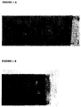
- the thickness of the film was equal to 500 nanometres. Owing to the absence of surface defects, a continuous and homogeneous coating of the sample with the metallic molybdenum film was possible, as shown in Figure 1A .
- the polyimide covering film was obtained by polycondensation from a solution of polyamidic acid in N-methylpyrrolidone, obtained from pyromellitic anhydride copolymerized with oxydianiline.
- the solution of the precursor at a concentration of 5% by weight, was applied by spin coating, onto the cementitious article in an amount proportional to the dimensions of the article itself, obtaining a layer of polymer solution with thickness of about 400 micrometres.
- the material was placed in an oven at a temperature of 120°C, in vacuum conditions of 67 kPa (500 mmHg), for a duration of one hour. Then the sample was subjected to a further heat treatment at 300°C, at atmospheric pressure, for two hours.
- the product, obtained according to the invention, has therefore ideal characteristics for photovoltaic applications.
- the sample was then subjected to a further heat treatment at 300°C, at atmospheric pressure, for two hours, in order to complete the in situ polymerization reaction.
- the article thus obtained without the pre-treatment according to the invention, was discontinuous and not homogeneous; the arithmetic mean surface roughness was equal to 530 micrometres, being therefore totally unsuitable for the manufacture of photovoltaic devices.
- the coated cementitious substrate obtained in Example 3 was introduced into a vacuum chamber of a sputtering device for deposition of a homogeneous film of metallic molybdenum, in order to produce a solar cell with a thin CIGS-based film. Owing to the presence of surface defects due to the lack of pre-treatment of the sample, a continuous and homogeneous coating of the sample with the metallic molybdenum film could not be obtained, as shown in Figure 1B .
Landscapes
- Chemical & Material Sciences (AREA)
- Engineering & Computer Science (AREA)
- Ceramic Engineering (AREA)
- Structural Engineering (AREA)
- Organic Chemistry (AREA)
- Materials Engineering (AREA)
- Civil Engineering (AREA)
- Architecture (AREA)
- Chemical Kinetics & Catalysis (AREA)
- Health & Medical Sciences (AREA)
- Toxicology (AREA)
- Photovoltaic Devices (AREA)
- Application Of Or Painting With Fluid Materials (AREA)
- Life Sciences & Earth Sciences (AREA)
- Sustainable Development (AREA)
- Sustainable Energy (AREA)
- Curing Cements, Concrete, And Artificial Stone (AREA)
- Manufacturing & Machinery (AREA)
Description
- The present invention relates in general to the field of cementitious articles and their use in the energy sector. Described herein are: a process for coating prefabricated cement articles, the articles obtained with said process, and their use in the construction sector, for non-structural applications, preferably as cladding and covering elements, both of the horizontal type and of the vertical type, with the aim of generating and/or transporting energy; said coated articles, having a small thickness and very low surface roughness, are in fact useful as substrates for deposition of metallic films and other thin films, during the construction of electrical devices such as solar cells, for example. The resultant products are of particular interest for applications in the field of Building Integrated Photovoltaics (BIPV), for aesthetic purposes and optimum integration of the photovoltaic modules in an urban context.
- Photovoltaic devices are being increasingly used in an urban context, as an integrative element in the construction sector, in order to produce useful amounts of alternative energy, thereby reducing the consumption of fossil fuels and the associated polluting emissions.
- For this purpose, for some time it has been widespread practice to mount solar panels on the external surfaces of buildings. This solution gives rise to significant problems from an aesthetic point of view, considering the poor imitative capacity of photovoltaic panels and the extensive surface area which must be exposed to solar radiation in order to obtain an appreciable return in energy terms.
- The solutions which have been proposed hitherto have been mainly aimed at improving the visual impact of the panel by improving its suitability for integration with the building components, for example by means of the inset arrangement of a panelled area within a roof. In such cases the negative aesthetic impact of the panel is only partially reduced. Moreover, a marked distinction between panel and construction material still remains, which obliges the builder to make specific constructional choices, limiting the freedom of choice as regards possible architectural solutions.
- The Applicant has since long been engaged in research into new methods useful for converting materials which are traditionally used in the building sector, into photovoltaic elements or parts thereof. Such an approach would improve the continuity between the constructional components and the photovoltaic elements, while improving the overall aesthetic appearance of the buildings.
- Japanese patent
JP 6184731 - The present invention relates to a process for the preparation of cementitious articles with a high surface finish, useful for the preparation of electrical, in particular photovoltaic devices, which are highly suitable for integration in the urban building sector. The process envisages the treatment of a prefabricated starting article, at specific temperature and pressure intervals, for a given time period, followed by coating of the article with a film based on a polymer selected from polyimide, polyarylketones or epoxy resins. Heat-resistant cementitious surfaces with an arithmetic mean surface roughness Ra which is very low, controlled and regular, without point-like defects, suitable for the deposition of additional thin films, are obtained. This solution is particularly advantageous where, as in most cases, the original cementitious articles do not satisfy the surface roughness requisites of the photovoltaic application. With the invention it is possible to produce cementitious articles such as flat slabs, sunshade elements, ventilated-façade elements, etc., which are obtained from cement-based mortars, cast or formed by means of compression in moulds, said articles being suitable for the deposition of additional thin, metallic and absorbent films, and therefore useful for the manufacture of photovoltaic cells and/or modules. In particular, the polymer coating applied according to the invention maintains unaltered the aforementioned surface properties even after exposure to the temperature and pressure process conditions required for the deposition of thin films of a metallic nature, for example based on molybdenum, and thin absorbent films, for example based on copper, indium (and gallium) diselenides, so-called CI(G)S, for the manufacture of thin-film photovoltaic devices.
-
-
Figure 1a shows the surface of a cementitious article coated with polyimide film and molybdenum metallic film, prepared in accordance with the treatment of the present invention. -
Figure 1b shows the surface of a cementitious article coated with polyimide film and molybdenum metallic film, obtained without the treatment according to the present invention. - In the context of the present invention, "low-thickness cementitious articles coated with polymer films having a high surface quality" are understood as meaning prefabricated three-dimensional objects which are to be used in the building sector for non-structural applications, coated with a suitable polymer film, synthesized on a solid material obtained from the hydration of cementitious compositions. "Low thickness" or "small thickness" is understood as meaning a thickness of between 0.1 cm and 5 cm, preferably between 0.2 and 1 cm, more preferably between 0.3 and 0.5 cm.
- The form of the cementitious starting article, used in the present invention, may vary greatly depending on the constructional needs; by way of a non-limiting example such forms may include those suitable for the manufacture of flat slabs, sunshade elements ventilated-façade elements, etc.
- In the process according to the invention, the cementitious starting article is not coated as such, but undergoes a pre-treatment in selected pressure conditions, of between 13 and 100 kPa (10 and 750 mmHg), preferably between 6.7 and 80 kPa (50 and 600 mmHg), more preferably between 13 and 67 kPa (100 and 500 mmHg), at a temperature of between 80 and 160°C, preferably between 100 and 150°C, more preferably between 110°C and 130°C, for a time period of between of 40 and 120 minutes, preferably between 45 and 90 minutes, more preferably between 50 and 70 minutes.
- Subsequently the article is coated with a polymer coating; preferably, this step follows directly the pre-treatment, namely without intermediate storage. The polymer coating may be applied in solution form, using techniques known per se, such as spin coating, atomization, sputtering, etc. A preferred technique is spin coating. The polymer of the coating is preferably polyimide. Alternative polymers which may be used are polyarylketones and epoxy resins.
- The surface of the article, which contains the polymer solution layer, is then consolidated and dried by subjecting the article to a heat treatment using known methods depending on the nature of the polymer.
- In a preferred method, the coating polymer is obtained directly on the surface of the article, depositing onto it a solution of a suitable precursor, which can be converted into said polymer by means of treatment in situ; in the case of polyimide, the precursor used is polyamide acid (obtained for example by means of copolymerization of suitable monomers such as biphenyltetracarboxylic dianhydride copolymerized with phenylenediamine, or from pyromellitic anhydride copolymerized with oxydianiline); the polyamide acid is converted in situ into polyimide by means of heat treatment, which involves dehydration of the polyamide acid and evaporation of the water formed; this treatment generally requires an initial heating at about 120°C, at a pressure of about 67 kPa (500 mmHg), for about 1 hour, followed by a secondary heating at about 300°C, at ambient pressure, for 1-2 hours.
- The thickness of the coating polymer solution applicable to the article is dependent on the roughness of the latter: for example, articles with an arithmetic mean surface roughness Ra of about 500 micrometres, coated with a thickness of 300 micrometres (or more) of a 5% by weight polymer coating solution result in the formation of surfaces with the required degree of regularity / uniformity for photovoltaic applications; the amount of coating required for articles with a different Ra may be calculated in a directly proportional manner from the aforementioned data.
- The arithmetic mean surface roughness (Ra) is a standard parameter which can be measured in an automated and reproducible manner by means of profilometers. The Ra values referred to here are obtained by means of a 3D Talysurf CCI optical profilometer, of the noncontact type, made by Taylor-Hobson, provided with automatic stage and autofocus. Alternative profilometers provide equivalent results. The system uses green-light scanning interferometry in order to obtain images and measurements of the parts analyzed, providing quantitive information on the structure of surfaces without physically contacting them. The light beam, after passing along the optical path of the microscope, is divided into two inside the interferometric lens. One part is reflected by the sample, while the other part is reflected by a high-quality reference surface present in the lens. The two beams are recombined and the resultant light is directed onto a solid-state telecamera. The interference between the two wave fronts generates an image formed by light and dark bands, called interference fringes, which are indicative of the surface structure of the analyzed part. Since the interference fringes originate only when the analyzed surface is in focus, it is necessary to perform a vertical scanning in order to be able to acquire the interferograms which characterize the height of each pixel forming the matrix of the CCD telecamera. Scanning is performed by means of a piezoelectric transducer situated at the base of the optical head of the microscope. The system is equipped with different types of lenses (50x, 20x, 10x, 5x, 2.5x), to be used in function of the surface characteristics of the sample to be examined. As the lens performs scanning, the telecamera records images of the intensity of the interference fringes. By means of an analysis of the frequency domain it is possible to locate the height for each pixel in a highly precise and specific manner. The measurements obtained are both three-dimensional and two-dimensional: the vertical measurement (perpendicular to the surface being examined) is obtained by means of interferometry, while the lateral measurements (in the plane of the sample) are obtained by means of calibration of the enlargement generated by the lens. The 3D data which characterize the surface and can be obtained using the technique described are as follows:
- height parameters: Sq, SSk, Sku, Sp, Sv, Sz, Sa, as defined according to the standard ISO 25178;
- planarity parameters: FLTt, FLTp, FLTv, FLTq, as defined according to the standard ISO 12781;
- The 2D data which characterize the surface and can be obtained using the technique described are as follows:
- height parameters: Rp, Rv, Rz, Rc, Rt, Ra, Rq, Rsk, Rku, as defined according to the standard ISO 4287;
- spacing parameters: RSm, Rdq, as defined according to the standard ISO 4287;
- peak parameters: RPc, as defined according to the standard ISO 4287.
- The value indicated above by Ra, among the height parameters, is the arithmetic mean surface roughness. Substrates which are useful for photovoltaic applications have Ra values preferably of between 10 and 150 nanometres, more preferably 30 and 90 nanometres. These values are advantageously obtained by the present invention, as shown in the tests below.
- The article coated with the consolidated polymer film may be coated with an additional metallic film, for example consisting of molybdenum, copper, aluminium, platinum, silver, gold, etc., and with an absorbent film, for example so-called CI(G)S, i.e. films based on copper, indium, (gallium), diselenides, for the manufacture of thin-film photovoltaic devices. The application of these additional films may be performed using technologies which are known per se, for example sputtering.
- As a result of the polymer coating applied in accordance with the present invention, the cementitious article does not require special production technologies and surface-finishing post-treatment in order to apply subsequently thin films for the manufacture of photovoltaic modules. The coating applied in accordance with the invention withstands effectively the vacuum and heating conditions which are typical of the thin-film deposition processes for photovoltaic applications, without losing the characteristics of adhesion to the cementitious substrate and without alteration of the surface properties thereof. The low roughness of the substrate coated in accordance with the invention is transferred to the superimposed thin (metallic, absorbent) films, resulting in a smooth and uniform final surface, of high value from an aesthetic point of view, stable over time in terms of adhesion, and resistant to the accumulation of dust and surface pollutants, with a performance which is reproducible over time.
- The present invention comprises cementitious articles as defined in claim 9 coated with a polymer film and optionally with further superimposed films, having a high surface finish, obtained by means of the process according to the invention. The articles have preferably a small thickness, in particular of between 0.1 and 5 cm. The invention is also applicable to the use of said articles for the preparation of electrical devices, in particular photovoltaic devices. The invention also includes the use of said articles for the manufacture of photocatalytically active cementitious building elements, for example slabs, sunshade elements, ventilated-façade elements, etc.
- The invention is now described in a non-limiting manner by the following examples.
- A prefabricated cementitious substrate with a thickness of 0.4 cm, previously obtained by casting a suitable mortar in moulds, was exposed to a pressure of 27 kPa (200 mmHg), at 120°C, for a time period of one hour.
- The polyimide covering film was obtained by polycondensation from a solution of polyamidic acid in N-methylpyrrolidone, obtained from biphenyltetracarboxylic dianhydride copolymerized with phenylenediamine.
- The solution of the precursor, at a concentration of 5% by weight, was applied by spin coating, onto the cementitious article in an amount proportional to the dimensions of the article itself, obtaining a layer of polymer solution with thickness of about 400 micrometres. After application, the material was placed in an oven at a temperature of 120°C, in vacuum conditions of 67 kPa (500 mmHg), for a duration of one hour. The sample was then subjected to a further heat treatment at 300°C, at atmospheric pressure, for two hours.
- After consolidation and drying, the analysis on an optical profilometer revealed a homogeneous and continuous resin layer. The thickness of the applied resin film was equal to 20 micrometres and its arithmetic mean surface roughness equal to 40 nanometres. The product, obtained according to the invention, has therefore ideal characteristics for photovoltaic applications.
- The coated cementitious substrate obtained in Example 1 was introduced into a vacuum chamber of a sputtering device for deposition of a homogeneous film of metallic molybdenum, in order to produce a solar cell with a thin CIGS-based film. The thickness of the film was equal to 500 nanometres. Owing to the absence of surface defects, a continuous and homogeneous coating of the sample with the metallic molybdenum film was possible, as shown in
Figure 1A . - A prefabricated cementitious substrate with thickness of 0.4 cm, previously obtained by casting a suitable mortar in moulds, was exposed to a pressure of 27 kPa (200 mmHg), at 120°C, for a time period of one hour.
- The polyimide covering film was obtained by polycondensation from a solution of polyamidic acid in N-methylpyrrolidone, obtained from pyromellitic anhydride copolymerized with oxydianiline.
- The solution of the precursor, at a concentration of 5% by weight, was applied by spin coating, onto the cementitious article in an amount proportional to the dimensions of the article itself, obtaining a layer of polymer solution with thickness of about 400 micrometres. The material was placed in an oven at a temperature of 120°C, in vacuum conditions of 67 kPa (500 mmHg), for a duration of one hour. Then the sample was subjected to a further heat treatment at 300°C, at atmospheric pressure, for two hours.
- After consolidation and drying, the analysis on a optical profilometer revealed a homogeneous and continuous resin layer. The thickness of the applied resin film was equal to 25 micrometres and its arithmetic mean surface roughness equal to 80 nanometres. The product, obtained according to the invention, has therefore ideal characteristics for photovoltaic applications.
- A solution of polyamidic acid, at a concentration of 5% by weight, obtained from biphenyltetracarboxylic dianhydride copolymerized with phenylenediamine, was directly applied by spin coating, in an amount proportional to the dimensions of the article itself, onto a cementitious substrate similar to the preceding ones, but not subjected to the pre-treatment according to the invention, obtaining a polymer solution layer with a thickness of about 400 micrometres. The material, after application, was placed in an oven at 120°C, in vacuum conditions of 67 kPa (500 mmHg), for a duration of one hour. The sample was then subjected to a further heat treatment at 300°C, at atmospheric pressure, for two hours, in order to complete the in situ polymerization reaction.
- The article thus obtained, without the pre-treatment according to the invention, was discontinuous and not homogeneous; the arithmetic mean surface roughness was equal to 530 micrometres, being therefore totally unsuitable for the manufacture of photovoltaic devices.
- The coated cementitious substrate obtained in Example 3 was introduced into a vacuum chamber of a sputtering device for deposition of a homogeneous film of metallic molybdenum, in order to produce a solar cell with a thin CIGS-based film. Owing to the presence of surface defects due to the lack of pre-treatment of the sample, a continuous and homogeneous coating of the sample with the metallic molybdenum film could not be obtained, as shown in
Figure 1B .
Claims (17)
- Process for the preparation of cementitious articles, with a high surface finish, suitable for the production of electrical devices, comprising:a) treating a cementitious article at pressure conditions of between 1.3 and 100 kPa (10 and 750 mmHg), at a temperature of between 80 and 160°C, for a time period of between 40 and 120 minutes and subsequentlyb) coating the surface of the article requiring finish with a film of a polymer selected from polyimide, polyarylketones or epoxy resins.
- Process according to claim 1, wherein step a) is carried out at a pressure of between 6.7 and 80 kPa (50 and 600 mmHg), at a temperature of between 100 and 150°C, for a time period of between 45 and 90 minutes.
- Process according to claim 1, wherein step a) is carried out at a pressure of between 13 and 67 kPa (100 and 500 mmHg), at a temperature of between 110 and 130°C, for a time period of between 50 and 70 minutes.
- Process according to any one of claims 1-3, wherein the coating in step b) is applied by spin coating.
- Process according to any one of claims 1-4, wherein the polymer in step b) is formed in situ on the surface of the cementitious article.
- Process according to any one of claims 1-5, wherein the article obtained in step b) is coated with one or more additional films, useful for electrical, in particular photovoltaic applications.
- Process according to any one of claims 1-6, wherein the polymer film obtained in b) has, after consolidation and drying, an arithmetic mean surface roughness Ra of between 30 and 90 nanometres.
- Process according to any one of claims 1-7, wherein the polymer film obtained in b) has, after consolidation and drying, a thickness of between 5 and 150 micrometres.
- Cementitious article with a high surface finish, suitable for the production of electrical devices, obtained by the process of claims 1-8, wherein the polymer film has, after consolidation and drying, an arithmetic mean surface roughness Ra of between 30 and 90 nanometres.
- Article according to claims 9, wherein the polymer film has, after consolidation and drying, a thickness of between 5 and 150 micrometres.
- Article according to any one of claims 9-10, with a thickness of between 0.1 and 5 cm.
- Article according to any one of claims 9-11, coated with one or more additional films, useful for electrical, in particular photovoltaic applications.
- Article according to any one of claims 9-12, in the form of a slab, sunshade element, ventilated-façade element, or any other element useful for application in Building Integrated Photovoltaics (BIPV).
- Electrical device comprising one or more articles according to claims 9-13.
- Device according to claim 14, said device being a photovoltaic device.
- Use of one or more articles according to claims 9-13 in the preparation of electrical, in particular photovoltaic devices.
- Use according to claim 16, wherein said devices are used in the field of Building Integrated Photovoltaics (BIPV).
Priority Applications (1)
| Application Number | Priority Date | Filing Date | Title |
|---|---|---|---|
| CY20161100377T CY1117572T1 (en) | 2011-10-27 | 2016-05-06 | PREPARATION OF Cementitious Objects with a High-Surface Surface Finish for Use in Electrical Devices |
Applications Claiming Priority (2)
| Application Number | Priority Date | Filing Date | Title |
|---|---|---|---|
| IT001950A ITMI20111950A1 (en) | 2011-10-27 | 2011-10-27 | PREPARATION OF CEMENT-BASED FINISHES WITH HIGH SURFACE FINISH FOR USE IN ELECTRICAL DEVICES |
| PCT/EP2012/004506 WO2013060477A1 (en) | 2011-10-27 | 2012-10-26 | Preparation of cementitious articles with a high surface finish for use in electrical devices |
Publications (2)
| Publication Number | Publication Date |
|---|---|
| EP2771306A1 EP2771306A1 (en) | 2014-09-03 |
| EP2771306B1 true EP2771306B1 (en) | 2016-02-24 |
Family
ID=44993732
Family Applications (1)
| Application Number | Title | Priority Date | Filing Date |
|---|---|---|---|
| EP12790399.5A Not-in-force EP2771306B1 (en) | 2011-10-27 | 2012-10-26 | Preparation of cementitious articles with a high surface finish for use in electrical devices |
Country Status (8)
| Country | Link |
|---|---|
| US (1) | US20140338740A1 (en) |
| EP (1) | EP2771306B1 (en) |
| CA (1) | CA2849550A1 (en) |
| CY (1) | CY1117572T1 (en) |
| ES (1) | ES2572971T3 (en) |
| IT (1) | ITMI20111950A1 (en) |
| MA (1) | MA35644B1 (en) |
| WO (1) | WO2013060477A1 (en) |
Families Citing this family (4)
| Publication number | Priority date | Publication date | Assignee | Title |
|---|---|---|---|---|
| FR3022240A1 (en) * | 2014-06-13 | 2015-12-18 | Lafarge Sa | CONCRETE COATED WITH A THIN PHOTOVOLTAIC THIN LAYER, PROCESS FOR PRODUCING THE SAME, AND CONSTRUCTION ELEMENT COMPRISING SUCH A CONCRETE |
| FR3025794A1 (en) * | 2014-09-15 | 2016-03-18 | Lafarge Sa | CONCRETE COATED WITH POLYMER LAYER DEPOSITED BY PLASMA TECHNOLOGY AND PROCESS FOR PRODUCING THE SAME |
| EP3205634A1 (en) | 2016-02-09 | 2017-08-16 | Holcim Technology Ltd. | Method of manufacturing a photovoltaic concrete |
| EP3453506A1 (en) | 2017-09-11 | 2019-03-13 | Holcim Technology Ltd. | Method of manufacturing a concrete element |
Family Cites Families (5)
| Publication number | Priority date | Publication date | Assignee | Title |
|---|---|---|---|---|
| DE1954013A1 (en) * | 1969-10-27 | 1971-05-06 | Incentive Aktiebolag | Plastic-coated concrete units with smooth - weather proof surface |
| JPH06184731A (en) | 1992-12-17 | 1994-07-05 | Mitsui Toatsu Chem Inc | Hard material having excellent design characteristic |
| US8438796B2 (en) * | 2007-11-06 | 2013-05-14 | Certainteed Corporation | Photovoltaic roofing elements including tie layer systems, and roofs using them, and methods for making them |
| JP2010095655A (en) * | 2008-10-17 | 2010-04-30 | Fujifilm Corp | Hydrophilic composition and hydrophilic member each having antifungal effect |
| IT1399627B1 (en) * | 2010-04-20 | 2013-04-26 | Italcementi Spa | CEMENTITIOUS MANUFACTURE SUITABLE FOR A PARTICULAR WHICH SUPPORT FOR A PHOTOVOLTAIC THIN FILM MODULE, AND METHOD FOR ITS PRODUCTION |
-
2011
- 2011-10-27 IT IT001950A patent/ITMI20111950A1/en unknown
-
2012
- 2012-10-26 EP EP12790399.5A patent/EP2771306B1/en not_active Not-in-force
- 2012-10-26 WO PCT/EP2012/004506 patent/WO2013060477A1/en not_active Ceased
- 2012-10-26 CA CA2849550A patent/CA2849550A1/en not_active Abandoned
- 2012-10-26 US US14/354,288 patent/US20140338740A1/en not_active Abandoned
- 2012-10-26 ES ES12790399.5T patent/ES2572971T3/en active Active
-
2014
- 2014-05-13 MA MA37026A patent/MA35644B1/en unknown
-
2016
- 2016-05-06 CY CY20161100377T patent/CY1117572T1/en unknown
Also Published As
| Publication number | Publication date |
|---|---|
| ES2572971T3 (en) | 2016-06-03 |
| CA2849550A1 (en) | 2013-05-02 |
| EP2771306A1 (en) | 2014-09-03 |
| US20140338740A1 (en) | 2014-11-20 |
| MA35644B1 (en) | 2014-11-01 |
| WO2013060477A1 (en) | 2013-05-02 |
| ITMI20111950A1 (en) | 2013-04-28 |
| CY1117572T1 (en) | 2017-04-26 |
Similar Documents
| Publication | Publication Date | Title |
|---|---|---|
| Lin et al. | High performance thin film solar cells on plastic substrates with nanostructure-enhanced flexibility | |
| Li et al. | Aqueous solution-chemical derived Ni–Al2O3 solar selective absorbing coatings | |
| US20140338740A1 (en) | Preparation of cementitious articles with a high surface finish for use in electrical devices | |
| Jyothi et al. | Optical properties of TiAlC/TiAlCN/TiAlSiCN/TiAlSiCO/TiAlSiO tandem absorber coatings by phase-modulated spectroscopic ellipsometry | |
| Sai et al. | Back surface reflectors with periodic textures fabricated by self-ordering process for light trapping in thin-film microcrystalline silicon solar cells | |
| Dan et al. | Temperature-and angle-dependent emissivity and thermal shock resistance of the W/WAlN/WAlON/Al2O3-based spectrally selective absorber | |
| AU2015396661B9 (en) | A polarization-independent SERS substrate | |
| Malwad et al. | Development and performance testing of reflector materials for concentrated solar power: A review | |
| Ji et al. | Flexible broadband plasmonic absorber on moth-eye substrate | |
| US20170148939A1 (en) | Cementitious product suitable in particular as substrate for a thin film photovoltaic module, and method of production thereof | |
| Sai et al. | Spectrally selective thermal radiators and absorbers with periodic microstructured surface for high-temperature applications | |
| EP2898113A2 (en) | Method for hardening a coating of a solar collector element, and elements produced by means of said method | |
| Volkan et al. | Optical and surface properties of LiFePO4 thin films prepared by RF magnetron sputtering | |
| Kalkowski et al. | Glass-glass direct bonding | |
| Avila-García et al. | Thermally and air–plasma-oxidized titanium and stainless steel plates as solar selective absorbers | |
| CN115513382A (en) | Perovskite thin film and preparation method thereof | |
| CN114799528A (en) | Method for remotely and rapidly preparing corrosion-resistant structure on irregular metal surface in large area | |
| CN116180009B (en) | Infrared broadband wave-absorbing metamaterial based on two-photon 3D printing and preparation method | |
| CN119036992B (en) | A low solar light absorption rate, high infrared emissivity aerospace thermal control film and its preparation method | |
| Abid et al. | Silver nano islands enhanced Raman scattering on large area grating substrates fabricated by two beam laser interference | |
| Ouyang et al. | Challenges of evaporated solid-phase-crystallised poly-Si thin-film solar cells on textured glass | |
| Shimizu et al. | High-temperature solar selective absorbers based on a transparent conductive oxide film coated periodic micro-hole array | |
| CN201292402Y (en) | Low-radiation film coating glass sputtering protection grooved bottom board | |
| Semchenko et al. | Reflectance of Black Silicon with Sol-Gel ZnO Passivation Films: Optical Simulation and Experimental Correlation | |
| CN117169850A (en) | A phase gradient metasurface and its preparation method and application |
Legal Events
| Date | Code | Title | Description |
|---|---|---|---|
| PUAI | Public reference made under article 153(3) epc to a published international application that has entered the european phase |
Free format text: ORIGINAL CODE: 0009012 |
|
| 17P | Request for examination filed |
Effective date: 20140416 |
|
| AK | Designated contracting states |
Kind code of ref document: A1 Designated state(s): AL AT BE BG CH CY CZ DE DK EE ES FI FR GB GR HR HU IE IS IT LI LT LU LV MC MK MT NL NO PL PT RO RS SE SI SK SM TR |
|
| DAX | Request for extension of the european patent (deleted) | ||
| GRAP | Despatch of communication of intention to grant a patent |
Free format text: ORIGINAL CODE: EPIDOSNIGR1 |
|
| INTG | Intention to grant announced |
Effective date: 20150608 |
|
| GRAS | Grant fee paid |
Free format text: ORIGINAL CODE: EPIDOSNIGR3 |
|
| GRAP | Despatch of communication of intention to grant a patent |
Free format text: ORIGINAL CODE: EPIDOSNIGR1 |
|
| INTG | Intention to grant announced |
Effective date: 20151030 |
|
| GRAA | (expected) grant |
Free format text: ORIGINAL CODE: 0009210 |
|
| AK | Designated contracting states |
Kind code of ref document: B1 Designated state(s): AL AT BE BG CH CY CZ DE DK EE ES FI FR GB GR HR HU IE IS IT LI LT LU LV MC MK MT NL NO PL PT RO RS SE SI SK SM TR |
|
| REG | Reference to a national code |
Ref country code: GB Ref legal event code: FG4D |
|
| REG | Reference to a national code |
Ref country code: CH Ref legal event code: EP |
|
| REG | Reference to a national code |
Ref country code: AT Ref legal event code: REF Ref document number: 776614 Country of ref document: AT Kind code of ref document: T Effective date: 20160315 |
|
| REG | Reference to a national code |
Ref country code: IE Ref legal event code: FG4D |
|
| REG | Reference to a national code |
Ref country code: DE Ref legal event code: R096 Ref document number: 602012015000 Country of ref document: DE |
|
| REG | Reference to a national code |
Ref country code: ES Ref legal event code: FG2A Ref document number: 2572971 Country of ref document: ES Kind code of ref document: T3 Effective date: 20160603 |
|
| REG | Reference to a national code |
Ref country code: LT Ref legal event code: MG4D |
|
| REG | Reference to a national code |
Ref country code: NL Ref legal event code: MP Effective date: 20160224 |
|
| REG | Reference to a national code |
Ref country code: AT Ref legal event code: MK05 Ref document number: 776614 Country of ref document: AT Kind code of ref document: T Effective date: 20160224 |
|
| PG25 | Lapsed in a contracting state [announced via postgrant information from national office to epo] |
Ref country code: FI Free format text: LAPSE BECAUSE OF FAILURE TO SUBMIT A TRANSLATION OF THE DESCRIPTION OR TO PAY THE FEE WITHIN THE PRESCRIBED TIME-LIMIT Effective date: 20160224 Ref country code: HR Free format text: LAPSE BECAUSE OF FAILURE TO SUBMIT A TRANSLATION OF THE DESCRIPTION OR TO PAY THE FEE WITHIN THE PRESCRIBED TIME-LIMIT Effective date: 20160224 Ref country code: NO Free format text: LAPSE BECAUSE OF FAILURE TO SUBMIT A TRANSLATION OF THE DESCRIPTION OR TO PAY THE FEE WITHIN THE PRESCRIBED TIME-LIMIT Effective date: 20160524 |
|
| PG25 | Lapsed in a contracting state [announced via postgrant information from national office to epo] |
Ref country code: LV Free format text: LAPSE BECAUSE OF FAILURE TO SUBMIT A TRANSLATION OF THE DESCRIPTION OR TO PAY THE FEE WITHIN THE PRESCRIBED TIME-LIMIT Effective date: 20160224 Ref country code: RS Free format text: LAPSE BECAUSE OF FAILURE TO SUBMIT A TRANSLATION OF THE DESCRIPTION OR TO PAY THE FEE WITHIN THE PRESCRIBED TIME-LIMIT Effective date: 20160224 Ref country code: PT Free format text: LAPSE BECAUSE OF FAILURE TO SUBMIT A TRANSLATION OF THE DESCRIPTION OR TO PAY THE FEE WITHIN THE PRESCRIBED TIME-LIMIT Effective date: 20160624 Ref country code: SE Free format text: LAPSE BECAUSE OF FAILURE TO SUBMIT A TRANSLATION OF THE DESCRIPTION OR TO PAY THE FEE WITHIN THE PRESCRIBED TIME-LIMIT Effective date: 20160224 Ref country code: LT Free format text: LAPSE BECAUSE OF FAILURE TO SUBMIT A TRANSLATION OF THE DESCRIPTION OR TO PAY THE FEE WITHIN THE PRESCRIBED TIME-LIMIT Effective date: 20160224 Ref country code: NL Free format text: LAPSE BECAUSE OF FAILURE TO SUBMIT A TRANSLATION OF THE DESCRIPTION OR TO PAY THE FEE WITHIN THE PRESCRIBED TIME-LIMIT Effective date: 20160224 Ref country code: AT Free format text: LAPSE BECAUSE OF FAILURE TO SUBMIT A TRANSLATION OF THE DESCRIPTION OR TO PAY THE FEE WITHIN THE PRESCRIBED TIME-LIMIT Effective date: 20160224 Ref country code: PL Free format text: LAPSE BECAUSE OF FAILURE TO SUBMIT A TRANSLATION OF THE DESCRIPTION OR TO PAY THE FEE WITHIN THE PRESCRIBED TIME-LIMIT Effective date: 20160224 |
|
| REG | Reference to a national code |
Ref country code: FR Ref legal event code: PLFP Year of fee payment: 5 |
|
| REG | Reference to a national code |
Ref country code: GR Ref legal event code: EP Ref document number: 20160400837 Country of ref document: GR Effective date: 20160601 |
|
| PG25 | Lapsed in a contracting state [announced via postgrant information from national office to epo] |
Ref country code: EE Free format text: LAPSE BECAUSE OF FAILURE TO SUBMIT A TRANSLATION OF THE DESCRIPTION OR TO PAY THE FEE WITHIN THE PRESCRIBED TIME-LIMIT Effective date: 20160224 Ref country code: DK Free format text: LAPSE BECAUSE OF FAILURE TO SUBMIT A TRANSLATION OF THE DESCRIPTION OR TO PAY THE FEE WITHIN THE PRESCRIBED TIME-LIMIT Effective date: 20160224 |
|
| REG | Reference to a national code |
Ref country code: DE Ref legal event code: R097 Ref document number: 602012015000 Country of ref document: DE |
|
| PG25 | Lapsed in a contracting state [announced via postgrant information from national office to epo] |
Ref country code: RO Free format text: LAPSE BECAUSE OF FAILURE TO SUBMIT A TRANSLATION OF THE DESCRIPTION OR TO PAY THE FEE WITHIN THE PRESCRIBED TIME-LIMIT Effective date: 20160224 Ref country code: SK Free format text: LAPSE BECAUSE OF FAILURE TO SUBMIT A TRANSLATION OF THE DESCRIPTION OR TO PAY THE FEE WITHIN THE PRESCRIBED TIME-LIMIT Effective date: 20160224 Ref country code: SM Free format text: LAPSE BECAUSE OF FAILURE TO SUBMIT A TRANSLATION OF THE DESCRIPTION OR TO PAY THE FEE WITHIN THE PRESCRIBED TIME-LIMIT Effective date: 20160224 Ref country code: CZ Free format text: LAPSE BECAUSE OF FAILURE TO SUBMIT A TRANSLATION OF THE DESCRIPTION OR TO PAY THE FEE WITHIN THE PRESCRIBED TIME-LIMIT Effective date: 20160224 |
|
| PLBE | No opposition filed within time limit |
Free format text: ORIGINAL CODE: 0009261 |
|
| STAA | Information on the status of an ep patent application or granted ep patent |
Free format text: STATUS: NO OPPOSITION FILED WITHIN TIME LIMIT |
|
| 26N | No opposition filed |
Effective date: 20161125 |
|
| PG25 | Lapsed in a contracting state [announced via postgrant information from national office to epo] |
Ref country code: SI Free format text: LAPSE BECAUSE OF FAILURE TO SUBMIT A TRANSLATION OF THE DESCRIPTION OR TO PAY THE FEE WITHIN THE PRESCRIBED TIME-LIMIT Effective date: 20160224 |
|
| REG | Reference to a national code |
Ref country code: CH Ref legal event code: PL |
|
| GBPC | Gb: european patent ceased through non-payment of renewal fee |
Effective date: 20161026 |
|
| REG | Reference to a national code |
Ref country code: IE Ref legal event code: MM4A |
|
| PG25 | Lapsed in a contracting state [announced via postgrant information from national office to epo] |
Ref country code: CH Free format text: LAPSE BECAUSE OF NON-PAYMENT OF DUE FEES Effective date: 20161031 Ref country code: GB Free format text: LAPSE BECAUSE OF NON-PAYMENT OF DUE FEES Effective date: 20161026 Ref country code: LI Free format text: LAPSE BECAUSE OF NON-PAYMENT OF DUE FEES Effective date: 20161031 |
|
| PG25 | Lapsed in a contracting state [announced via postgrant information from national office to epo] |
Ref country code: LU Free format text: LAPSE BECAUSE OF NON-PAYMENT OF DUE FEES Effective date: 20161026 |
|
| REG | Reference to a national code |
Ref country code: FR Ref legal event code: PLFP Year of fee payment: 6 |
|
| PGFP | Annual fee paid to national office [announced via postgrant information from national office to epo] |
Ref country code: IT Payment date: 20170921 Year of fee payment: 6 Ref country code: GR Payment date: 20170929 Year of fee payment: 6 Ref country code: FR Payment date: 20170921 Year of fee payment: 6 |
|
| PG25 | Lapsed in a contracting state [announced via postgrant information from national office to epo] |
Ref country code: IE Free format text: LAPSE BECAUSE OF NON-PAYMENT OF DUE FEES Effective date: 20161026 |
|
| PGFP | Annual fee paid to national office [announced via postgrant information from national office to epo] |
Ref country code: BG Payment date: 20170921 Year of fee payment: 6 Ref country code: BE Payment date: 20170922 Year of fee payment: 6 |
|
| PGFP | Annual fee paid to national office [announced via postgrant information from national office to epo] |
Ref country code: DE Payment date: 20170920 Year of fee payment: 6 |
|
| PGFP | Annual fee paid to national office [announced via postgrant information from national office to epo] |
Ref country code: CY Payment date: 20170920 Year of fee payment: 6 Ref country code: ES Payment date: 20171103 Year of fee payment: 6 |
|
| PG25 | Lapsed in a contracting state [announced via postgrant information from national office to epo] |
Ref country code: HU Free format text: LAPSE BECAUSE OF FAILURE TO SUBMIT A TRANSLATION OF THE DESCRIPTION OR TO PAY THE FEE WITHIN THE PRESCRIBED TIME-LIMIT; INVALID AB INITIO Effective date: 20121026 |
|
| PG25 | Lapsed in a contracting state [announced via postgrant information from national office to epo] |
Ref country code: IS Free format text: LAPSE BECAUSE OF FAILURE TO SUBMIT A TRANSLATION OF THE DESCRIPTION OR TO PAY THE FEE WITHIN THE PRESCRIBED TIME-LIMIT Effective date: 20160224 Ref country code: MK Free format text: LAPSE BECAUSE OF FAILURE TO SUBMIT A TRANSLATION OF THE DESCRIPTION OR TO PAY THE FEE WITHIN THE PRESCRIBED TIME-LIMIT Effective date: 20160224 Ref country code: MT Free format text: LAPSE BECAUSE OF NON-PAYMENT OF DUE FEES Effective date: 20161031 Ref country code: MC Free format text: LAPSE BECAUSE OF FAILURE TO SUBMIT A TRANSLATION OF THE DESCRIPTION OR TO PAY THE FEE WITHIN THE PRESCRIBED TIME-LIMIT Effective date: 20160224 |
|
| PG25 | Lapsed in a contracting state [announced via postgrant information from national office to epo] |
Ref country code: TR Free format text: LAPSE BECAUSE OF FAILURE TO SUBMIT A TRANSLATION OF THE DESCRIPTION OR TO PAY THE FEE WITHIN THE PRESCRIBED TIME-LIMIT Effective date: 20160224 Ref country code: AL Free format text: LAPSE BECAUSE OF FAILURE TO SUBMIT A TRANSLATION OF THE DESCRIPTION OR TO PAY THE FEE WITHIN THE PRESCRIBED TIME-LIMIT Effective date: 20160224 |
|
| REG | Reference to a national code |
Ref country code: DE Ref legal event code: R119 Ref document number: 602012015000 Country of ref document: DE |
|
| REG | Reference to a national code |
Ref country code: BE Ref legal event code: FP Effective date: 20160511 Ref country code: BE Ref legal event code: MM Effective date: 20181031 |
|
| PG25 | Lapsed in a contracting state [announced via postgrant information from national office to epo] |
Ref country code: DE Free format text: LAPSE BECAUSE OF NON-PAYMENT OF DUE FEES Effective date: 20190501 Ref country code: CY Free format text: LAPSE BECAUSE OF NON-PAYMENT OF DUE FEES Effective date: 20181026 |
|
| PG25 | Lapsed in a contracting state [announced via postgrant information from national office to epo] |
Ref country code: GR Free format text: LAPSE BECAUSE OF NON-PAYMENT OF DUE FEES Effective date: 20190506 Ref country code: BE Free format text: LAPSE BECAUSE OF NON-PAYMENT OF DUE FEES Effective date: 20181031 Ref country code: FR Free format text: LAPSE BECAUSE OF NON-PAYMENT OF DUE FEES Effective date: 20181031 Ref country code: BG Free format text: LAPSE BECAUSE OF NON-PAYMENT OF DUE FEES Effective date: 20190430 |
|
| PG25 | Lapsed in a contracting state [announced via postgrant information from national office to epo] |
Ref country code: IT Free format text: LAPSE BECAUSE OF NON-PAYMENT OF DUE FEES Effective date: 20181026 |
|
| REG | Reference to a national code |
Ref country code: ES Ref legal event code: FD2A Effective date: 20191203 |
|
| PG25 | Lapsed in a contracting state [announced via postgrant information from national office to epo] |
Ref country code: ES Free format text: LAPSE BECAUSE OF NON-PAYMENT OF DUE FEES Effective date: 20181027 |