EP2769467B1 - Resonator with reduced acceleration sensitivity and phase noise using time domain switch - Google Patents
Resonator with reduced acceleration sensitivity and phase noise using time domain switch Download PDFInfo
- Publication number
- EP2769467B1 EP2769467B1 EP12842190.6A EP12842190A EP2769467B1 EP 2769467 B1 EP2769467 B1 EP 2769467B1 EP 12842190 A EP12842190 A EP 12842190A EP 2769467 B1 EP2769467 B1 EP 2769467B1
- Authority
- EP
- European Patent Office
- Prior art keywords
- oscillator
- position switch
- relative position
- resonator
- oscillation
- Prior art date
- Legal status (The legal status is an assumption and is not a legal conclusion. Google has not performed a legal analysis and makes no representation as to the accuracy of the status listed.)
- Not-in-force
Links
Images








Classifications
-
- H—ELECTRICITY
- H03—ELECTRONIC CIRCUITRY
- H03H—IMPEDANCE NETWORKS, e.g. RESONANT CIRCUITS; RESONATORS
- H03H9/00—Networks comprising electromechanical or electro-acoustic elements; Electromechanical resonators
- H03H9/02—Details
- H03H9/02244—Details of microelectro-mechanical resonators
- H03H9/02433—Means for compensation or elimination of undesired effects
-
- H—ELECTRICITY
- H03—ELECTRONIC CIRCUITRY
- H03H—IMPEDANCE NETWORKS, e.g. RESONANT CIRCUITS; RESONATORS
- H03H9/00—Networks comprising electromechanical or electro-acoustic elements; Electromechanical resonators
- H03H9/24—Constructional features of resonators of material which is not piezoelectric, electrostrictive, or magnetostrictive
- H03H9/2405—Constructional features of resonators of material which is not piezoelectric, electrostrictive, or magnetostrictive of microelectro-mechanical resonators
-
- H—ELECTRICITY
- H03—ELECTRONIC CIRCUITRY
- H03H—IMPEDANCE NETWORKS, e.g. RESONANT CIRCUITS; RESONATORS
- H03H9/00—Networks comprising electromechanical or electro-acoustic elements; Electromechanical resonators
- H03H9/02—Details
- H03H9/02244—Details of microelectro-mechanical resonators
- H03H9/02259—Driving or detection means
- H03H2009/02267—Driving or detection means having dimensions of atomic scale, e.g. involving electron transfer across vibration gap
Definitions
- Existing resonators employ a variety of physical mechanisms to create usable resonance for timing applications. Examples include structural mode resonance and bulk acoustic wave resonance for example. Existing technologies, however, all suffer in timing accuracy due to sensitivities to external vibrations (i.e., perturbations, accelerations, etc.) and contain a time-dependent phase noise. These drawbacks reduce the accuracy and usefulness of resonators for timing applications either as discrete components or embedded within existing electronic circuitry fabricated on a semiconducting substrate for example. Phase noise, or jitter of the output resonator frequency, can be due to the capacitive method of sensing the resonance thus resulting in a sinusoidal output. This sinusoidal output can be noisy in nature due to noise introduced by the transduction technique, for example.
- US 2004/187577 discloses a vibration type angular velocity sensor which, to cancel inphase components acting on vibrators of first and second sensor units in an angular velocity sensing direction, comprises a differential amplification circuit that obtains a differential waveform between a first angular velocity sensing waveform and a second angular velocity sensing waveform.
- the present invention provides a resonator and a method for providing a resonator with a relative position switch, as set out in claims 1 and 12 respectively.
- a robust, low-cost and high resolution dual oscillator resonator and methods of implementing and using the same.
- One embodiment of the resonator which comprises a frame, first and second oscillators, first and second relative position switch halves, and a driver.
- the first oscillator is configured to oscillate with respect to the frame and the first driver is configured to drive the first oscillator at the first oscillator's resonant frequency.
- the first and second oscillators have the same resonant frequency and are designed to respond in substantially the same manner to external perturbations to the frame.
- the first and second halves of the relative position switch are mounted to the first and second oscillators respectively. As the first oscillator oscillates there is relative motion between the first and second oscillators such that the relative position switch passes through a closed state in each oscillation when the first and second switch halves pass by each other.
- Also described herein is a method for providing a resonator with a relative position switch.
- the method begins by providing a frame and configuring a first oscillator to oscillate with respect to the frame. Next the first oscillator is driven at the first oscillator's resonant frequency. In other steps, a first half of a relative position switch is mounted to the first oscillator and a second oscillator is provided which has the same resonant frequency as the first oscillator.
- the first and second oscillators are designed to respond in substantially the same manner to external perturbations to the frame. When the first oscillator oscillates there is relative motion between the first and second oscillators.
- a second half of the relative position switch is mounted to the second oscillator such that as the first and second switch halves pass by each other in each oscillation the relative position switch passes through a closed state. Then a period of oscillation is determined as the difference between successive closed states of the relative position switch.
- top,” bottom, side, up,” “down”, “left,” “right,” and the like merely connote a relative position or geometry of one component to another, and in no way connote an absolute frame of reference or any required orientation.
- a “top” portion of a component may actually reside below a “bottom” portion when the component is mounted to another device (e.g., to the underside of a PCB).
- Figure 1 depict a top view of an embodiment of a resonator 10 that has reduced phase noise and minimal sensitivity to external perturbations and/or other phenomena.
- the resonator 10 comprises a frame 12, first and second oscillators 14 and 16 respectively, first and second relative position switch halves i 8 and 20 respectively, and a driver 22 (shown in Figs. 2A-2C ).
- the driver 22 is configured to drive the first oscillator 14 at the first oscillator's resonant frequency.
- the resonator 10 is configured such that when the first oscillator 14 oscillates with respect to the frame 12 there is relative motion between the first and second oscillators 14 and 16.
- the first and second relative position switch halves 18 and 20 are mounted to the first and second oscillators 14 and 16 respectively in any configuration such that during each oscillation of the first oscillator 14 the relative position switch passes through a closed state when the first and second relative position switch halves 18 and 20 pass by each other.
- the first and second oscillators 14 and 16, which have substantially the same resonant frequency, are designed to respond in substantially the same manner to external perturbations to the frame 12.
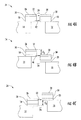
- Figures 2A-2C are side/cross-sectional views of one embodiment of the resonator 10 showing various possible positions of the first oscillator 14 as it oscillates with respect to the frame 12.
- Figure 2B depicts the first and second relative position switch halves 18 and 20 in the closed state.
- Figures 2A and 2C depict the first and second relative position switch halves 18 and 20 in an open state.
- Figures 2A-2C also show an embodiment of the driver 22 where the driver 22 is an electrode positioned above the first oscillator 14.
- the frame 12 may have any desired size and/or shape and may have any structure that is capable of supporting the first and second oscillators 14 and 16.
- the resonator 10 and its components may all be monolithically manufactured as a micro-electro-mechanical system (MEMS).
- MEMS micro-electro-mechanical system
- Suitable materials out of which the frame may be constructed include, but are not limited to silicon, Gallium Arsenide (GaAs), and other semiconductor materials, as well as quartz, PZT, and other piezoelectric materials.
- first and second oscillators 14 and 16 may be coupled to the frame 12 in any way that allows them to oscillate with respect to the frame 12 such that there is relative motion between the first and second oscillators 14 and 16.
- oscillator refers generally, and without limitation, to an assembly configured for periodic or aperiodic displacement with respect to a reference position.
- first and second oscillators 14 and 16 include, but are not limited to, clamped-clamped beam resonators, tuning fork resonators, asymmetric resonators, symmetrically anchored resonators, bulk disk resonators, and lateral-mode resonators.
- One or both of the first and second oscillators 14 and 16 may be driven.
- both resonators may be locked 180 degrees out of phase with one another.
- only the first oscillator 14 is driven by the driver 22 to oscillate at its resonant frequency and the second oscillator 16 remains substantially stationary except for external perturbations and vibrations from the first oscillator 14 which are communicated through the frame 12 to the second resonator 16.
- the first and second relative position switch halves 18 and 20 are thin planar scanning tunneling microscopy (STM) tips fabricated on the edges of the first and second oscillators 14 and 16.
- STM scanning tunneling microscopy
- the relative position switch halves 18 and 20 may be any two elements capable of generating a detectable impulse or change in reference during each oscillation as the first and second relative position switch halves 18 and 20 pass by each other.
- the purpose of the relative position switch is to localize the position of the first and second oscillators 14 and 16 such that an accurate acceleration-independent phase measurement can be performed thereby increasing stability of a phased-locked loop closure and reducing overall phase noise and jitter of the resonator 10.
- the relative position switch is an electron tunneling switch a finite width pulse is generated.
- the current pulse itself can be amplified to the rails via a transimpedance amplifier and the leading and or trailing edges of the pulse used to localize the position and provide information with regards to the time dependent position of the resonator, as is described more fully with respect to Figures 6A and 6B and Table 1 below.
- the relative position switch may also be a capacitive switch, which would work by generating a time-dependent charge as the first and second relative position switch halves 18 and 20 change overlap area with one another. This change can be integrated and amplified to the rails in a similar fashion as the tunneling current previously described.
- switches could be used such as optical shuttering between a light source and a detector or magnetic switches disposed on the first and second oscillators 14 and 16.
- the relative position switch may also function by sensing the field emission of electrons or the thermionic emission between the first and second relative position switch halves 18 and 20.
- an optical light source may be used to provide photo-assisted tunneling to enhance tunneling currents or thermionic currents in the relative position switch. To save power the light source could be pulsed synchronously with the resonant frequency such that light is only emitted during a period of time in which the first and second relative position switch halves 18 and 20 are aligned or are close to being in alignment.
- the first and second relative position switch halves 18 and 20 are thin planar STM tips such as is shown in Figures 1 and 2A-2B
- the first and second relative position switch halves 18 and 20 are separated by a narrow gap 24 which represents a high potential region.
- Any differential voltage on the first relative position switch half 18 should produce a pulse of current when it passes a grounded conductive plane of the second relative position switch half 20.
- the width W of the gap 24 may be, but is not limited to, less than ten angstroms. This configuration (i.e. tip-to-tip and/or edge to edge) differs from other typical STM configurations where current "tunnels" between a charged planar surface of atoms and a point tip.
- the driver 22 may be any device capable of driving the first oscillator 14 to oscillate with respect to the frame 12.
- the driver 22 may be a driving circuit which provides a driving signal configured to induce the oscillatory motion in the first oscillator 14 which, turn, displaces the first switch half 18 with respect to the second half 20.
- Another suitable example of the driver 22 includes, but is not limited to, an electrode positioned above and below the first oscillator 14, such as is shown in Figures 2A-2C .
- the first oscillator 14 may also be driven by a constant electrical signal generated through feedback circuitry to maintain resonant oscillation.
- Yet another example of the driver 22 includes a device for applying a short duration electrical voltage to an electrode positioned either above or below the first oscillator 14.
- the driving signal from the driver 22 includes a time-gated (or "pinged") signal that is turned on and off (e.g., periodically).
- the oscillation of the oscillator 14 is caused by using a stepped electrostatic force to initiate harmonic oscillation.
- the electrostatic force is short in duration compared to the resonant frequency of the oscillator 14 thus providing a "pushing" reinforcement that keeps the oscillator 14 in resonance. This force is periodically repeated as necessary to ensure that the amplitude of the oscillator stays above a minimum value at which point another electrostatic pulse or "ping" is applied.
- the first oscillator 14 is driven in a continuous fashion, such as via a time-varying wave function.
- the driver 22 could also comprise a piezoelectric transducer deposited on a cantilever spring embodiment of the resonator 10.
- the resonator 10 is configured to provide digital (time-based) output, rather than an analog signal output. Such configuration ensures that the accuracy of the resonator 10 is only dependent on the consistency of the triggering events, the nature of the oscillation (whether harmonic, or alternatively non-harmonic), and the accuracy of the time measurement of adjacent triggered events. Since the triggering events are based on the physical dimensions established during fabrication, the proposed design advantageously does not require continuing calibration; i.e., is "self calibrating".
- Resonators that rely on time-varying displacement of a mass at a characteristic frequency can be modeled as mass-spring systems. Accordingly, such systems are subject to external accelerations and forces, which can perturb the accuracy of the phase and periodicity of the resonance-thereby impacting the closed-loop control circuitry. This situation leads to an acceleration-dependence for all MEMS-based resonators.
- the resonator 10 addresses these shortcomings.
- Figures 3A-3D show various example embodiments of first and second relative position switch halves 18 and 20 as electron tunneling tips.
- a trigger signal may be generated by a sensing circuit, indicating a closed switch state.
- two electron tunneling electrodes (one fixed to each of the first and second oscillators 14 and 16) are used as the two switch halves and the signal includes a tunneling discharge pulse caused by the close proximity of electrode tips when the electrodes are aligned in the closed switch position.
- Figure 3A depicts rectangular tips.
- Figure 3B depicts circular tips.
- Figure 3C depicts triangular tips.
- Figure 3D depicts isosceles trapezoidal tips.
- the shape of the tunneling tips may be anything that produces a geometric field enhancement or that increases the tunneling area.
- Figures 4A-4C show side-view illustrations of multiple relative position switches stacked on top of one another, wherein the first and second oscillators 14 and 16 are in various trigger positions.
- Figures 4A-4C show third and fourth relative position switch halves 26 and 28 stacked on top of the first and second relative position switch halves 18 and 20 respectively.
- the stacked switch halves are separated by a dielectric material 30.
- Standard monolithic printed circuit fabrication techniques may be used to fabricate this embodiment of the resonator 10. For every oscillation cycle of the oscillator 14, whenever the relative position switch halves 18, 20, 26. and 28 pass through any of the three trigger positions, tunneling discharge current pulses are induced across the gaps 24 between two or more relative position switch halves, or electrodes.
- the three trigger positions in this embodiment include a zero force point position 34, a positive displacement (+ d 0) position 36, and a negative displacement (- d 0) position 38 (shown in Figures 4A, 4B, and 4C respectively).
- tunneling discharge current pulses 40, 42, and 44 When the first and second oscillators 14 and 16 are aligned in the positive displacement position 36, the zero force point position 34, or the negative displacement position 38, tunneling discharge current pulses 40, 42, and 44 are induced respectively.
- the tunneling discharge current pulses 40, 42, and 44 may be sensed and may be amplified by low-noise current amplifiers as described in further detail with respect to Figure 5 , below.
- Figure 5 shows how the tunneling discharge current pulses 40, 42, and 44 may be amplified to the rails.
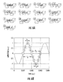
- FIGS 6A-6B illustrate an exemplary sequence of a tunneling pulse generation for the embodiment of resonator 10 shown in Figure 4A-4C .
- This sequence comprises one complete cycle of oscillation of the first oscillator 14.
- the position-indicator circles with white backgrounds 1, 3, 5, 7, 9, 11, and 13 in Figures 6A and 6B indicate the tip positions where a conducting path is established for current flow (i.e., trigger positions 34, 36, and 38), which may be equated to instances of logical "1s.”
- the position indicator circles with shaded backgrounds 2, 4, 6, 8, 10, and 12 correspond to positions where there is no conducting current, which may be equated to instances of logical "0s.”
- the oscillator 14 is in the zero force position 34 (e.g., positions 1, 7, and 13) both relative position switches are aligned, hence causing current pulses 42 between relative position switch halves 18 and 20 and between switch halves 26 and 28.
- the current pulse 40 is generated between the first relative position switch half 18 and the fourth relative position switch half 28.
- the current pulse 44 is generated between the third relative position switch half 26 and the second relative position switch half 20.
- Figures 7-8 are plots of the oscillation amplitude over time of the first and second oscillators 14 and 16 wherein the first oscillator 14 is driven on resonance and the second oscillator 16 is not driven.
- Trace 52 represents the oscillation of the first oscillator 14.
- Trace 54 represents the oscillation of the second oscillator 16.
- Figure 7 shows how the first and second oscillators 14 and 16 respond similarly to an external perturbation.
- Figure 8 shows that the crossing points of the first and second oscillators 14 and 16 always results in substantially the same measured time period, T .
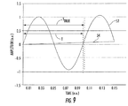
- Figure 9 is a plot of the oscillation amplitude over time of the first and second oscillators 14 and 16. This figure shows that when the period, T , of the first oscillator 14 is measured with respect to the frame 12 an error in measured period occurs.
- the true period, Tirue is given be the crossings of the two oscillators.
- the driving frequency ⁇ drv is configured to match the natural resonance frequency ⁇ 0 of the first oscillator 14 causing a sinusoidal motion of the first oscillator 14, as shown in Figures 7-9 .
- a system driven-in-resonance typically requires a high-quality factor ( Q ) oscillating proof-mass system. It will be appreciated, however, that for this embodiment, literally any driving signal that maintains the oscillator in resonance may be used.
- the first oscillator 14 is driven "off-resonance", which provides, inter alia, precise control of the oscillation period and, hence, control of sensor accuracy. Off-resonance driven systems typically require a lower Q oscillator.
- Non-harmonic embodiments of the first and second oscillators 14 and 16 may also be used with this invention as long as they are driven at the same frequency and out of phase with one another.
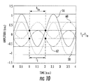
- Figure 10 is a plot showing the oscillations of the first and second oscillators 14 and 16 with and without applied external acceleration.
- the oscillation amplitude over time of the first oscillator 14 when the frame 12 is subject to applied external acceleration is represented by the solid trace 56.
- the oscillation amplitude over time of the first oscillator 14 without applied external acceleration to the frame 12 is represented by the dotted line 58.
- the oscillation amplitude over time of the second oscillator 16 when the frame 12 is subject to applied external acceleration is represented by the sinusoidal dashed line 60.
- the oscillation amplitude over time of the second oscillator 16 without applied external acceleration to the frame 12 is represented by the dotted-dashed line 62.
- the period, T1a represents the distance between oscillation crossing points of the first and second oscillators 14 and 16 when subjected to external acceleration.
- the period T1 represents the distance between oscillation crossing points of the first and second oscillators 14 and 16 without applied external acceleration.
- T 1a substantially equals T1.
- the frequency of oscillation of the first oscillator 14 and the second oscillator 16 may thus be determined by recording the time between two successive triggering events.
- Typical MEMS resonators are driven and sensed capacitively or with a piezoelectric transducer which means the ability to implement a phased locked loop (PLL) is dependent on the ability to accurately measure the precise phase, i.e. the amplitude of the sinusoidal charge generated from a capacitive signal or a sinusoidal voltage generated from a piezoelectric transducer.
- the resonator 10 has a well defined trigger between the first and second oscillators 14 and 16 at a known moment in time that is substantially independent of acceleration, as shown in Figure 10 , thus allowing the PLL to be closed more accurately and in a more robust manner than previous resonators.
- Figure 11 shows a top view of another embodiment of the resonator 10.
- the first and second oscillators 14 and 16 are mounted to the same side of the frame 12 and the first and second relative position switch halves 18 and 20 are planar conductors having parallel edges separated from each other by the gap 24.
- first and second absolute position switch halves 64 and 66 are also shown in this embodiment.
- the first half 64 of the absolute position switch is mounted to the frame 12 and the second half 66 is mounted to the first oscillator 14. In this manner, acceleration of the frame 12 can be independently measured.
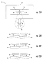
- Figures 12A-12D show another embodiment of the resonator 10.
- Figure 12A is a top view showing the first and second oscillators 14 and 16 mounted to opposite sides of the frame 12.
- Figures 12B-12D are side views of the embodiment of the resonator 10 shown in Figure 12A which show exaggerated illustrations of the relative motion between the first and second oscillators 14 and 16. In this embodiment, both oscillators 14 and 16 are driven 180 out of phase with each other by the driver 22.
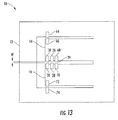
- Figure 13 portrays a top view of another embodiment of the resonator 10.
- the first relative position switch comprises the first and second switch halves 18 and 20.
- the second relative position switch comprises the third and forth switch halves 26 and 28.
- the third relative position switch comprises fifth and sixth relative position switch halves 68 and 70.
- the first absolute position switch comprises the first and second switch halves 64 and 66.
- the first absolute position switch half 64 is mounted to the frame 12 and the second absolute position switch half 66 is mounted to an edge of the first oscillator 14.
- the second absolute position switch comprises third and fourth switch halves 72 and 74.
- the third absolute position switch half 72 is mounted to an edge of the second oscillator 16.
- the fourth absolute position switch half 74 is mounted to the frame.
- Figures 14A-14B are operational block diagrams of two different embodiments of the resonator 10.
- Figure 14A illustrates the operation of the resonator 10 where only the first oscillator 14 is driven.
- the driver 22 drives the first oscillator 14 and produces a voltage bias 75 as an analog output. That analog output 75 may be fed into a frequency detector 76 which produces an output 78.
- the output 78 is received by a low pass filter 80 which in turn, produces a filtered signal 82. which is then received by the driver 22.
- the relative position switch 80 produces a current pulse 82 during every closed state of the relative position switch 80.
- the current pulse 82 is a digital output which may be fed back into the frequency detector 76.
- Figure 14B illustrates the operation of the embodiment of the resonator 10 where the second oscillator 16 is also driven by the driver 22. As shown in Figure 14B , the driving output 75 is phase shifted by a phase shifter 84 before it reaches the second oscillator 16.
- Figures 15A, 15B, 16A, 16B, and 17 show several plots of the oscillation amplitudes over time of an embodiment of the resonator 10 where both the first and second oscillators 14 and 16 are driven by the driver 22. When both oscillators are driven there does not need to be 180 degrees phase difference between them, but merely a phase difference.
- Figure 15A shows the oscillations of the first and second oscillators 14 and 16 with a phase difference of ⁇ radians.
- Figure 15B shows the oscillations of the first and second oscillators 14 and 16 with a phase difference of ⁇ /1.2 radians.
- Figure 16A shows the oscillations of the first and second oscillators 14 and 16 with a phase difference of ⁇ /1.4 radians.
- Figure 16B shows the oscillations of the first and second oscillators 14 and 16 with a phase difference of ⁇ /2 radians.
- Figure 17 shows the oscillations of the first and second oscillators 14 and 16 with a phase difference of ⁇ /4
- the resonator 10 may be implemented as a printed circuit with no moving parts.
- various features of the resonator 10 may be implemented as software routines or instructions to be executed on a processing device (e.g. a general purpose processor, application specific integrated circuit (ASIC), field programmable gate array (FPGA), etc.)
- ASIC application specific integrated circuit
- FPGA field programmable gate array
Landscapes
- Physics & Mathematics (AREA)
- Acoustics & Sound (AREA)
- Oscillators With Electromechanical Resonators (AREA)
- Piezo-Electric Or Mechanical Vibrators, Or Delay Or Filter Circuits (AREA)
- Micromachines (AREA)
- Gyroscopes (AREA)
Description
- Existing resonators employ a variety of physical mechanisms to create usable resonance for timing applications. Examples include structural mode resonance and bulk acoustic wave resonance for example. Existing technologies, however, all suffer in timing accuracy due to sensitivities to external vibrations (i.e., perturbations, accelerations, etc.) and contain a time-dependent phase noise. These drawbacks reduce the accuracy and usefulness of resonators for timing applications either as discrete components or embedded within existing electronic circuitry fabricated on a semiconducting substrate for example. Phase noise, or jitter of the output resonator frequency, can be due to the capacitive method of sensing the resonance thus resulting in a sinusoidal output. This sinusoidal output can be noisy in nature due to noise introduced by the transduction technique, for example. When a noise sinusoidal output is fed back into the resonator via a phase-locked loop (PLL) or delay- locked loop (DLL) control loop the result is instability in the feedback circuitry. In addition, because the signals are measured capacitively or based on the piezoelectric effect they can be sensitive to external vibrations or anything that may cause a time-dependent deformation of the resonant mode-shape, frequency or phase of the signal. Current resonators lack effective means to independently measure or cancel-out this environmental noise contribution.
-
US 2004/187577 discloses a vibration type angular velocity sensor which, to cancel inphase components acting on vibrators of first and second sensor units in an angular velocity sensing direction, comprises a differential amplification circuit that obtains a differential waveform between a first angular velocity sensing waveform and a second angular velocity sensing waveform. - The present invention provides a resonator and a method for providing a resonator with a relative position switch, as set out in
claims - Described herein are several embodiments of a robust, low-cost and high resolution dual oscillator resonator, and methods of implementing and using the same. One embodiment of the resonator is disclosed which comprises a frame, first and second oscillators, first and second relative position switch halves, and a driver. The first oscillator is configured to oscillate with respect to the frame and the first driver is configured to drive the first oscillator at the first oscillator's resonant frequency. The first and second oscillators have the same resonant frequency and are designed to respond in substantially the same manner to external perturbations to the frame. The first and second halves of the relative position switch are mounted to the first and second oscillators respectively. As the first oscillator oscillates there is relative motion between the first and second oscillators such that the relative position switch passes through a closed state in each oscillation when the first and second switch halves pass by each other.
- Also described herein is a method for providing a resonator with a relative position switch. The method begins by providing a frame and configuring a first oscillator to oscillate with respect to the frame. Next the first oscillator is driven at the first oscillator's resonant frequency. In other steps, a first half of a relative position switch is mounted to the first oscillator and a second oscillator is provided which has the same resonant frequency as the first oscillator. The first and second oscillators are designed to respond in substantially the same manner to external perturbations to the frame. When the first oscillator oscillates there is relative motion between the first and second oscillators. A second half of the relative position switch is mounted to the second oscillator such that as the first and second switch halves pass by each other in each oscillation the relative position switch passes through a closed state. Then a period of oscillation is determined as the difference between successive closed states of the relative position switch.
- Other features and advantages of the present disclosure will immediately be recognized by persons of ordinary skill in the art with reference to the attached drawings and detailed description of exemplary embodiments as given below.
- Throughout the several views, like elements are referenced using like references. The elements in the figures are not drawn to scale and some dimensions are exaggerated for clarity. As used herein, the terms "top," "bottom," "side," "up," "down", "left," "right," and the like merely connote a relative position or geometry of one component to another, and in no way connote an absolute frame of reference or any required orientation. For example, a "top" portion of a component may actually reside below a "bottom" portion when the component is mounted to another device (e.g., to the underside of a PCB).
-
Figure 1 is a top view of an embodiment of a resonator. -
Figure 2A is a side view of an embodiment of a resonator showing deflection of oscillators. -
Figure 2B is a side view of an embodiment of a resonator showing aligned oscillators. -
Figure 2C is a side view of an embodiment of a resonator showing deflection of oscillators. -
Figures 3A-3D are top views of various embodiments of electron tunneling tips. -
Figures 4A-4C are side views of an embodiment of a resonator having stacked relative position switch halves. -
Figure 5 is a plot of the oscillation amplitude over time of an oscillator with stacked relative position switch halves. -
Figure 6A is an illustration showing various relative positions of two oscillators during the oscillation of one of the oscillators. -
Figure 6B is a plot of the oscillation amplitude over time of the resonator depicted inFigure 6A . -
Figure 7 is a plot of the oscillation amplitude over time of one embodiment of a dual-oscillator resonator. -
Figure 8 is a plot of the oscillation amplitude over time of another embodiment of a dual-oscillator resonator. -
Figure 9 is a plot of the oscillation amplitude over time of another embodiment of a dual-oscillator resonator. -
Figure 10 is a plot of the oscillation amplitude over time of another embodiment of a dual-oscillator resonator. -
Figure 11 is a top view of another embodiment of a dual-oscillator resonator. -
Figure 12A is a top view of another embodiment of a dual-oscillator resonator. -
Figures 12B-12C are side views of the embodiment of the dual-oscillator resonator depicted inFigure 12A . -
Figure 13 is a top view of another embodiment of a dual-oscillator resonator. -
Figures 14A and 14B are operational block diagrams of different embodiments of a dual-oscillator resonator. -
Figures 15A-15B are plots of the oscillation amplitudes over time of two oscillators from different embodiments of a dual-oscillator resonator. -
Figures 16A-16B are plots of the oscillation amplitudes over time of two oscillators from different embodiments of a dual-oscillator resonator. -
Figure 17 is a plot of the oscillation amplitudes over time of two oscillators from an embodiment of a dual-oscillator resonator. -
Figure 1 depict a top view of an embodiment of aresonator 10 that has reduced phase noise and minimal sensitivity to external perturbations and/or other phenomena. Theresonator 10 comprises aframe 12, first andsecond oscillators Figs. 2A-2C ). Thedriver 22 is configured to drive thefirst oscillator 14 at the first oscillator's resonant frequency. Theresonator 10 is configured such that when thefirst oscillator 14 oscillates with respect to theframe 12 there is relative motion between the first andsecond oscillators position switch halves second oscillators first oscillator 14 the relative position switch passes through a closed state when the first and second relativeposition switch halves second oscillators frame 12. -
Figures 2A-2C are side/cross-sectional views of one embodiment of theresonator 10 showing various possible positions of thefirst oscillator 14 as it oscillates with respect to theframe 12.Figure 2B depicts the first and second relativeposition switch halves Figures 2A and 2C depict the first and second relativeposition switch halves Figures 2A-2C also show an embodiment of thedriver 22 where thedriver 22 is an electrode positioned above thefirst oscillator 14. - The
frame 12 may have any desired size and/or shape and may have any structure that is capable of supporting the first andsecond oscillators resonator 10 and its components may all be monolithically manufactured as a micro-electro-mechanical system (MEMS). Suitable materials out of which the frame may be constructed include, but are not limited to silicon, Gallium Arsenide (GaAs), and other semiconductor materials, as well as quartz, PZT, and other piezoelectric materials. - It is to be understood that the first and
second oscillators Figures 1 and 2A-2C as cantilever spring elements, may be coupled to theframe 12 in any way that allows them to oscillate with respect to theframe 12 such that there is relative motion between the first andsecond oscillators second oscillators second oscillators second oscillators first oscillator 14 is driven by thedriver 22 to oscillate at its resonant frequency and thesecond oscillator 16 remains substantially stationary except for external perturbations and vibrations from thefirst oscillator 14 which are communicated through theframe 12 to thesecond resonator 16. - In the embodiment of the
resonator 10 shown inFigures 1 and 2A-2C , the first and second relative position switch halves 18 and 20 are thin planar scanning tunneling microscopy (STM) tips fabricated on the edges of the first andsecond oscillators second oscillators resonator 10. In the embodiment of theresonator 10 where the relative position switch is an electron tunneling switch a finite width pulse is generated. The current pulse itself can be amplified to the rails via a transimpedance amplifier and the leading and or trailing edges of the pulse used to localize the position and provide information with regards to the time dependent position of the resonator, as is described more fully with respect toFigures 6A and 6B and Table 1 below. The relative position switch may also be a capacitive switch, which would work by generating a time-dependent charge as the first and second relative position switch halves 18 and 20 change overlap area with one another. This change can be integrated and amplified to the rails in a similar fashion as the tunneling current previously described. Other switches could be used such as optical shuttering between a light source and a detector or magnetic switches disposed on the first andsecond oscillators - Continuing now with the embodiment of the
resonator 10 where the first and second relative position switch halves 18 and 20 are thin planar STM tips such as is shown inFigures 1 and 2A-2B , when the relative position switch is in the closed state, the first and second relative position switch halves 18 and 20 are separated by anarrow gap 24 which represents a high potential region. Any differential voltage on the first relativeposition switch half 18 should produce a pulse of current when it passes a grounded conductive plane of the second relativeposition switch half 20. Only when the first andsecond oscillators Figure 2B would current "tunnel" across thegap 24. The width W of thegap 24 may be, but is not limited to, less than ten angstroms. This configuration (i.e. tip-to-tip and/or edge to edge) differs from other typical STM configurations where current "tunnels" between a charged planar surface of atoms and a point tip. - The
driver 22 may be any device capable of driving thefirst oscillator 14 to oscillate with respect to theframe 12. For example, thedriver 22 may be a driving circuit which provides a driving signal configured to induce the oscillatory motion in thefirst oscillator 14 which, turn, displaces thefirst switch half 18 with respect to thesecond half 20. Another suitable example of thedriver 22 includes, but is not limited to, an electrode positioned above and below thefirst oscillator 14, such as is shown inFigures 2A-2C . Thefirst oscillator 14 may also be driven by a constant electrical signal generated through feedback circuitry to maintain resonant oscillation. Yet another example of thedriver 22 includes a device for applying a short duration electrical voltage to an electrode positioned either above or below thefirst oscillator 14. In one approach, the driving signal from thedriver 22 includes a time-gated (or "pinged") signal that is turned on and off (e.g., periodically). In other words, the oscillation of theoscillator 14 is caused by using a stepped electrostatic force to initiate harmonic oscillation. The electrostatic force is short in duration compared to the resonant frequency of theoscillator 14 thus providing a "pushing" reinforcement that keeps theoscillator 14 in resonance. This force is periodically repeated as necessary to ensure that the amplitude of the oscillator stays above a minimum value at which point another electrostatic pulse or "ping" is applied. In another approach, thefirst oscillator 14 is driven in a continuous fashion, such as via a time-varying wave function. Thedriver 22 could also comprise a piezoelectric transducer deposited on a cantilever spring embodiment of theresonator 10. - The
resonator 10 is configured to provide digital (time-based) output, rather than an analog signal output. Such configuration ensures that the accuracy of theresonator 10 is only dependent on the consistency of the triggering events, the nature of the oscillation (whether harmonic, or alternatively non-harmonic), and the accuracy of the time measurement of adjacent triggered events. Since the triggering events are based on the physical dimensions established during fabrication, the proposed design advantageously does not require continuing calibration; i.e., is "self calibrating". - Resonators that rely on time-varying displacement of a mass at a characteristic frequency can be modeled as mass-spring systems. Accordingly, such systems are subject to external accelerations and forces, which can perturb the accuracy of the phase and periodicity of the resonance-thereby impacting the closed-loop control circuitry. This situation leads to an acceleration-dependence for all MEMS-based resonators. The
resonator 10 addresses these shortcomings. In classical mechanics, a harmonic oscillator is a system that, when displaced from its equilibrium position, experiences a restoring force F that is proportional to the displacement x as:

- k is the spring constant;
- m is the oscillator mass
- ƒ0 is the oscillator resonant frequency; and
- T0 is the corresponding period of oscillations.
-
Figures 3A-3D show various example embodiments of first and second relative position switch halves 18 and 20 as electron tunneling tips. When thefirst switch half 18 is aligned with thesecond switch half 20, a trigger signal may be generated by a sensing circuit, indicating a closed switch state. In one exemplary implementation, two electron tunneling electrodes (one fixed to each of the first andsecond oscillators 14 and 16) are used as the two switch halves and the signal includes a tunneling discharge pulse caused by the close proximity of electrode tips when the electrodes are aligned in the closed switch position.Figure 3A depicts rectangular tips.Figure 3B depicts circular tips.Figure 3C depicts triangular tips.Figure 3D depicts isosceles trapezoidal tips. However, it is to be understood that in the embodiment of theresonator 10 where the first and second relative position switch halves 18 and 20 are electron tunneling tips, the shape of the tunneling tips may be anything that produces a geometric field enhancement or that increases the tunneling area. -
Figures 4A-4C show side-view illustrations of multiple relative position switches stacked on top of one another, wherein the first andsecond oscillators Figures 4A-4C show third and fourth relative position switch halves 26 and 28 stacked on top of the first and second relative position switch halves 18 and 20 respectively. The stacked switch halves are separated by adielectric material 30. Standard monolithic printed circuit fabrication techniques may be used to fabricate this embodiment of theresonator 10. For every oscillation cycle of theoscillator 14, whenever the relative position switch halves 18, 20, 26. and 28 pass through any of the three trigger positions, tunneling discharge current pulses are induced across thegaps 24 between two or more relative position switch halves, or electrodes. The three trigger positions in this embodiment include a zeroforce point position 34, a positive displacement (+d0)position 36, and a negative displacement (-d0) position 38 (shown inFigures 4A, 4B, and 4C respectively). When the first andsecond oscillators positive displacement position 36, the zeroforce point position 34, or thenegative displacement position 38, tunneling dischargecurrent pulses current pulses Figure 5 , below. -
Figure 5 shows how the tunneling dischargecurrent pulses 
- I is output current;
- U is the applied tunneling bias voltage;
- d is the tunneling gap width;
- K is a constant describing density of available states both source and destination; and
- β is a constant describing the electron work function or the energy that is required to free an electron to vacuum potential.
-
Figures 6A-6B illustrate an exemplary sequence of a tunneling pulse generation for the embodiment ofresonator 10 shown inFigure 4A-4C . This sequence comprises one complete cycle of oscillation of thefirst oscillator 14. The position-indicator circles withwhite backgrounds Figures 6A and 6B indicate the tip positions where a conducting path is established for current flow (i.e., trigger positions 34, 36, and 38), which may be equated to instances of logical "1s." The position indicator circles withshaded backgrounds oscillator 14 is in the zero force position 34 (e.g., positions 1, 7, and 13) both relative position switches are aligned, hence causingcurrent pulses 42 between relative position switch halves 18 and 20 and between switch halves 26 and 28. When theoscillator 14 is in the positive displacement position 36 (denoted with thedesignators 3 and 5), thecurrent pulse 40 is generated between the first relativeposition switch half 18 and the fourth relativeposition switch half 28. Similarly, when theoscillator 14 is in the negative displacement position 38 (denoted with thedesignators 9 and 11), thecurrent pulse 44 is generated between the third relativeposition switch half 26 and the second relativeposition switch half 20. When theoscillator 14 is in the positions denoted with thedesignators -
Figures 7-8 are plots of the oscillation amplitude over time of the first andsecond oscillators first oscillator 14 is driven on resonance and thesecond oscillator 16 is not driven.Trace 52 represents the oscillation of thefirst oscillator 14.Trace 54 represents the oscillation of thesecond oscillator 16.Figure 7 shows how the first andsecond oscillators Figure 8 shows that the crossing points of the first andsecond oscillators -
Figure 9 is a plot of the oscillation amplitude over time of the first andsecond oscillators first oscillator 14 is measured with respect to theframe 12 an error in measured period occurs. The true period, Tirue, is given be the crossings of the two oscillators. - In one embodiment of the
resonator 10, the driving frequency ƒdrv is configured to match the natural resonance frequency ƒ0 of thefirst oscillator 14 causing a sinusoidal motion of thefirst oscillator 14, as shown inFigures 7-9 . A system driven-in-resonance typically requires a high-quality factor (Q) oscillating proof-mass system. It will be appreciated, however, that for this embodiment, literally any driving signal that maintains the oscillator in resonance may be used. In another embodiment (not shown), thefirst oscillator 14 is driven "off-resonance", which provides, inter alia, precise control of the oscillation period and, hence, control of sensor accuracy. Off-resonance driven systems typically require a lower Q oscillator. Non-harmonic embodiments of the first andsecond oscillators -
Figure 10 is a plot showing the oscillations of the first andsecond oscillators first oscillator 14 when theframe 12 is subject to applied external acceleration is represented by thesolid trace 56. The oscillation amplitude over time of thefirst oscillator 14 without applied external acceleration to theframe 12 is represented by the dottedline 58. The oscillation amplitude over time of thesecond oscillator 16 when theframe 12 is subject to applied external acceleration is represented by the sinusoidal dashedline 60. The oscillation amplitude over time of thesecond oscillator 16 without applied external acceleration to theframe 12 is represented by the dotted-dashedline 62. The period, T1a, represents the distance between oscillation crossing points of the first andsecond oscillators second oscillators Figure 10 , T 1a substantially equals T1. Thus, the application of an external force to theresonator 10 does not substantially affect the timing between crossings. The frequency of oscillation of thefirst oscillator 14 and thesecond oscillator 16 may thus be determined by recording the time between two successive triggering events. Typical MEMS resonators are driven and sensed capacitively or with a piezoelectric transducer which means the ability to implement a phased locked loop (PLL) is dependent on the ability to accurately measure the precise phase, i.e. the amplitude of the sinusoidal charge generated from a capacitive signal or a sinusoidal voltage generated from a piezoelectric transducer. Theresonator 10 has a well defined trigger between the first andsecond oscillators Figure 10 , thus allowing the PLL to be closed more accurately and in a more robust manner than previous resonators. -
Figure 11 shows a top view of another embodiment of theresonator 10. In this embodiment, the first andsecond oscillators frame 12 and the first and second relative position switch halves 18 and 20 are planar conductors having parallel edges separated from each other by thegap 24. Also shown in this embodiment are first and second absolute position switch halves 64 and 66. Thefirst half 64 of the absolute position switch is mounted to theframe 12 and thesecond half 66 is mounted to thefirst oscillator 14. In this manner, acceleration of theframe 12 can be independently measured. -
Figures 12A-12D show another embodiment of theresonator 10.Figure 12A is a top view showing the first andsecond oscillators frame 12.Figures 12B-12D are side views of the embodiment of theresonator 10 shown inFigure 12A which show exaggerated illustrations of the relative motion between the first andsecond oscillators oscillators driver 22. -
Figure 13 portrays a top view of another embodiment of theresonator 10. In this embodiment, there are three relative position switches mounted to the first andsecond oscillators halves position switch half 64 is mounted to theframe 12 and the second absoluteposition switch half 66 is mounted to an edge of thefirst oscillator 14. The second absolute position switch comprises third and fourth switch halves 72 and 74. The third absoluteposition switch half 72 is mounted to an edge of thesecond oscillator 16. The fourth absoluteposition switch half 74 is mounted to the frame. -
Figures 14A-14B are operational block diagrams of two different embodiments of theresonator 10.Figure 14A illustrates the operation of theresonator 10 where only thefirst oscillator 14 is driven. In this embodiment, thedriver 22 drives thefirst oscillator 14 and produces avoltage bias 75 as an analog output. Thatanalog output 75 may be fed into afrequency detector 76 which produces anoutput 78. Theoutput 78 is received by alow pass filter 80 which in turn, produces a filteredsignal 82. which is then received by thedriver 22. As thefirst oscillator 14 oscillates, therelative position switch 80 produces acurrent pulse 82 during every closed state of therelative position switch 80. Thecurrent pulse 82 is a digital output which may be fed back into thefrequency detector 76.Figure 14B illustrates the operation of the embodiment of theresonator 10 where thesecond oscillator 16 is also driven by thedriver 22. As shown inFigure 14B , the drivingoutput 75 is phase shifted by aphase shifter 84 before it reaches thesecond oscillator 16. -
Figures 15A, 15B, 16A, 16B, and 17 show several plots of the oscillation amplitudes over time of an embodiment of theresonator 10 where both the first andsecond oscillators driver 22. When both oscillators are driven there does not need to be 180 degrees phase difference between them, but merely a phase difference.Figure 15A shows the oscillations of the first andsecond oscillators Figure 15B shows the oscillations of the first andsecond oscillators Figure 16A shows the oscillations of the first andsecond oscillators Figure 16B shows the oscillations of the first andsecond oscillators Figure 17 shows the oscillations of the first andsecond oscillators - From the above description of the
resonator 10 it is manifest that various techniques may be used for implementing the concepts of theresonator 10 without departing from its scope. For example, in one embodiment, theresonator 10 may be implemented as a printed circuit with no moving parts. Further, various features of theresonator 10 may be implemented as software routines or instructions to be executed on a processing device (e.g. a general purpose processor, application specific integrated circuit (ASIC), field programmable gate array (FPGA), etc.) The described embodiments are to be considered in all respects as illustrative and not restrictive. It should also be understood that theresonator 10 is not limited to the particular embodiments described herein, but is capable of many embodiments without departing from the scope of the claims.
Claims (15)
- A resonator (10) comprising:a frame (12);a first oscillator (14) configured to oscillate with respect to the frame;a first driver (22) configured to drive the first oscillator at the first oscillator's resonant frequency;a first half (18) of a first relative position switch mounted to the first oscillator;a second oscillator (16) having the same resonant frequency as the first oscillator, wherein the first and second oscillators are designed to respond in substantially the same manner to external perturbations to the frame;a second half (20) of the first relative position switch mounted to the second oscillator,characterised in thatas the first oscillator oscillates there is relative motion between the first and second oscillators such that the first relative position switch passes through a closed state in each oscillation when the first and second switch halves of the first relative position switch pass by each other.
- The resonator of claim 1, further comprising a second driver configured to drive the second oscillator at the second oscillator's resonant frequency and out of phase with the first oscillator.
- The resonator of claim 1, wherein the second oscillator (16) is not driven.
- The resonator of claim 1, wherein the first relative position switch is configured to pass an electrical impulse when in its closed state during each oscillation.
- The resonator of claim 4, wherein the first (18) and second (20) halves of the first relative position switch comprise planar conductors.
- The resonator of claim 5,wherein the planar conductors each comprise a substantially straight edge and wherein the edges are substantially parallel, and wherein when the first relative position switch is in the closed state, the edges are separated from each other by a narrow gap (24).
- The resonator of claim 1, wherein the first relative position switch is a capacitive switch.
- The resonator of claim 1, wherein the first relative position switch is configured to produce a binary change of an electrical signal when in its closed state during each oscillation such that the output of the resonator is a digital signal.
- The resonator of claim 1, wherein the first driver comprises feedback circuitry configured to generate an electrical signal to maintain operation on resonance.
- The resonator of claim 1, further comprising an absolute position switch comprising first and second halves, wherein the first half of the absolute position switch is mounted to the first oscillator and the second half of the absolute position switch is mounted to the frame such that the absolute position switch passes through a closed state during each oscillation of the first oscillator.
- The resonator of claim 1, further comprising a second relative position switch having first and second halves, wherein the first and second halves of the second relative position switch are disposed above the first and second halves of the first relative position switch respectively such that a current may pass from any given relative position switch half on the first oscillator to any of the relative position switch halves on the second oscillator to which the given relative position switch half is aligned.
- A method for providing a resonator (10) with a relative position switch, the method comprising:providing a frame (12);configuring a first oscillator (14) to oscillate with respect to the frame;driving the first oscillator at the first oscillator's resonant frequency;mounting a first half (18) of a relative position switch to the first oscillator;providing a second oscillator (16) having the same resonant frequency as the first oscillator, wherein the first and second oscillators are designed to respond in substantially the same manner to external perturbations to the frame;mounting a second half (20) of the relative position switch to the second oscillator,characterised in thatwhen the first oscillator oscillates there is relative motion between the first and second oscillators, and as the first and second switch halves pass by each other in each oscillation the relative position switch passes through a closed state; anddetermining a period of oscillation as the difference between successive closed states of the relative position switch.
- The method of claim 12, further comprising the step of driving the second oscillator to oscillate at the second oscillator's resonant frequency out of phase with the first oscillator
- The method of claim 12, further comprising the step of mounting an absolute position switch to the first oscillator and the frame such that the absolute position switch passes through a closed state during each oscillation of the first oscillator.
- The method of claim 14, further comprising the step of determining a time-varying acceleration based on an output of the absolute position switch and compensating the oscillation period for skew based on the time-varying acceleration.
Applications Claiming Priority (2)
| Application Number | Priority Date | Filing Date | Title |
|---|---|---|---|
| US13/276,948 US8427249B1 (en) | 2011-10-19 | 2011-10-19 | Resonator with reduced acceleration sensitivity and phase noise using time domain switch |
| PCT/US2012/058794 WO2013058993A1 (en) | 2011-10-19 | 2012-10-04 | Resonator with reduced acceleration sensitivity and phase noise using time domain switch |
Publications (4)
| Publication Number | Publication Date |
|---|---|
| EP2769467A1 EP2769467A1 (en) | 2014-08-27 |
| EP2769467A4 EP2769467A4 (en) | 2015-04-22 |
| EP2769467B1 true EP2769467B1 (en) | 2016-09-28 |
| EP2769467B8 EP2769467B8 (en) | 2016-12-21 |
Family
ID=48094842
Family Applications (1)
| Application Number | Title | Priority Date | Filing Date |
|---|---|---|---|
| EP12842190.6A Not-in-force EP2769467B8 (en) | 2011-10-19 | 2012-10-04 | Resonator with reduced acceleration sensitivity and phase noise using time domain switch |
Country Status (5)
| Country | Link |
|---|---|
| US (1) | US8427249B1 (en) |
| EP (1) | EP2769467B8 (en) |
| JP (2) | JP2014533009A (en) |
| TW (2) | TWI536622B (en) |
| WO (1) | WO2013058993A1 (en) |
Families Citing this family (21)
| Publication number | Priority date | Publication date | Assignee | Title |
|---|---|---|---|---|
| US7956621B2 (en) * | 2008-06-11 | 2011-06-07 | Analog Devices, Inc. | Anti-capture method and apparatus for micromachined devices |
| US8505382B2 (en) * | 2011-02-10 | 2013-08-13 | Ut-Battelle, Llc | Nonlinear nanomechanical oscillators for ultrasensitive inertial detection |
| US9705450B2 (en) | 2011-06-24 | 2017-07-11 | The United States Of America As Represented By The Secretary Of The Navy | Apparatus and methods for time domain measurement of oscillation perturbations |
| US9128496B2 (en) | 2011-10-26 | 2015-09-08 | The United States Of America As Represented By Secretary Of The Navy | Auto-ranging for time domain extraction of perturbations to sinusoidal oscillation |
| US8683862B2 (en) * | 2011-11-03 | 2014-04-01 | The United States Of America As Represented By The Secretary Of The Navy | Oscillation apparatus with atomic-layer proximity switch |
| US8650955B2 (en) * | 2012-01-18 | 2014-02-18 | The United States Of America As Represented By The Secretary Of The Navy | Time domain switched gyroscope |
| US8991250B2 (en) * | 2012-09-11 | 2015-03-31 | The United States Of America As Represented By Secretary Of The Navy | Tuning fork gyroscope time domain inertial sensor |
| EP3103191B1 (en) * | 2014-02-07 | 2018-07-11 | The Regents of the University of California | Frequency tuning and/or frequency tracking of a mechanical system with low sensitivity to electrical feedthrough |
| FI126019B (en) * | 2014-02-12 | 2016-05-31 | Murata Manufacturing Co | Drive circuit for a MEMS resonator |
| FI126557B (en) * | 2014-05-07 | 2017-02-15 | Murata Manufacturing Co | Improved gyroscope structure and gyroscope |
| WO2015200846A2 (en) | 2014-06-26 | 2015-12-30 | Lumedyne Technologies Incorporated | Systems and methods for extracting system parameters from nonlinear periodic signals from sensors |
| CN107636473B (en) * | 2015-05-20 | 2020-09-01 | 卢米达因科技公司 | Extract inertial information from nonlinear periodic signals |
| WO2017004443A2 (en) * | 2015-06-30 | 2017-01-05 | Lumedyne Technologies Incorporated | Z-axis physical proximity switch |
| US9577633B1 (en) * | 2016-06-17 | 2017-02-21 | The United States Of America As Represented By Secretary Of The Navy | Capacitive charge triggered proximity switch for use with time domain switched inertial sensors |
| US20180031603A1 (en) * | 2016-07-27 | 2018-02-01 | Lumedyne Technologies Incorporated | Systems and methods for detecting inertial parameters using a vibratory accelerometer with multiple degrees of freedom |
| US10234477B2 (en) | 2016-07-27 | 2019-03-19 | Google Llc | Composite vibratory in-plane accelerometer |
| US9977046B2 (en) | 2016-08-08 | 2018-05-22 | The United States Of America As Represented By The Secretary Of The Navy | Pinch contact switch for determining bending surface states |
| CN112334867B (en) | 2018-05-24 | 2025-11-11 | 纽约州立大学研究基金会 | Capacitive sensor |
| US10823759B2 (en) * | 2018-11-05 | 2020-11-03 | Xilinx, Inc. | Test system and method of testing a wafer for integrated circuit devices |
| JP6961638B2 (en) * | 2019-03-14 | 2021-11-05 | 株式会社東芝 | Sensor module |
| CN113111527A (en) * | 2021-04-20 | 2021-07-13 | 华北电力大学 | Approximate analysis method for switching type frequency oscillation of single-machine hydroelectric system |
Family Cites Families (24)
| Publication number | Priority date | Publication date | Assignee | Title |
|---|---|---|---|---|
| JPS5545232A (en) * | 1978-09-26 | 1980-03-29 | Seiko Instr & Electronics Ltd | Piezo-electric vibrator |
| US5023503A (en) | 1990-01-03 | 1991-06-11 | Motorola, Inc. | Super high frequency oscillator/resonator |
| JP3158825B2 (en) * | 1993-12-21 | 2001-04-23 | 富士電機株式会社 | Acceleration sensor |
| WO1995019571A1 (en) * | 1994-01-18 | 1995-07-20 | Siemens Aktiengesellschaft | Tunnel effect sensor |
| GB9524241D0 (en) * | 1995-11-28 | 1996-01-31 | Smiths Industries Plc | Rate sensors |
| EP1313215B1 (en) * | 1999-11-02 | 2012-05-02 | ETA SA Manufacture Horlogère Suisse | Temperature compensation mechanism for a micromechanical ring resonator |
| US6636655B2 (en) * | 2000-08-29 | 2003-10-21 | Memscap S.A. | MEMS optical switches having obliquely angled inputs and outputs relative to a face thereof and moveable reflectors with parallel positions therein and methods of forming same |
| EP1217735B1 (en) * | 2000-12-21 | 2007-11-14 | ETA SA Manufacture Horlogère Suisse | Time base comprising an integrated micromechanical tuning fork resonator |
| GB0116393D0 (en) * | 2001-07-05 | 2001-08-29 | Druck Ltd | Improved sensor |
| US6718825B1 (en) * | 2003-01-17 | 2004-04-13 | Honeywell International Inc. | Methods and systems for reducing stick-down within MEMS structures |
| JP2004317484A (en) * | 2003-03-31 | 2004-11-11 | Denso Corp | Vibration type angular velocity sensor |
| KR100599115B1 (en) * | 2004-07-20 | 2006-07-12 | 삼성전자주식회사 | Vibration type MEMS switch and manufacturing method |
| US7280078B2 (en) * | 2004-11-20 | 2007-10-09 | Scenterra, Inc. | Sensor for detecting high frequency signals |
| WO2006055960A2 (en) * | 2004-11-20 | 2006-05-26 | Scenterra, Inc. | Device for emission of high frequency signals |
| JP4887034B2 (en) * | 2005-12-05 | 2012-02-29 | 日立オートモティブシステムズ株式会社 | Inertial sensor |
| US8502198B2 (en) * | 2006-04-28 | 2013-08-06 | Hewlett-Packard Development Company, L.P. | Switching device and methods for controlling electron tunneling therein |
| US7332849B2 (en) * | 2006-05-19 | 2008-02-19 | Nanyang Technological University | Method and transducers for dynamic testing of structures and materials |
| GB2439606B (en) * | 2006-06-29 | 2011-08-17 | C Mac Quartz Crystals Ltd | An oscillator |
| US7444868B2 (en) * | 2006-06-29 | 2008-11-04 | Honeywell International Inc. | Force rebalancing for MEMS inertial sensors using time-varying voltages |
| JP5105345B2 (en) * | 2006-09-04 | 2012-12-26 | セイコーインスツル株式会社 | Oscillator |
| JP4432990B2 (en) * | 2007-03-22 | 2010-03-17 | セイコーエプソン株式会社 | Sensor and electronic equipment |
| EP2375428A3 (en) | 2008-10-01 | 2012-12-05 | Joseph F. Pinkerton | Nanoelectromechanical tunneling current membraneswitch |
| US8188800B2 (en) * | 2008-11-07 | 2012-05-29 | Greenray Industries, Inc. | Crystal oscillator with reduced acceleration sensitivity |
| US8629795B2 (en) * | 2009-09-09 | 2014-01-14 | Taiwan Semiconductor Manufacturing Company, Ltd. | Micro-electro-mechanical systems (MEMS), systems, and operating methods thereof |
-
2011
- 2011-10-19 US US13/276,948 patent/US8427249B1/en active Active
-
2012
- 2012-10-04 JP JP2014537097A patent/JP2014533009A/en active Pending
- 2012-10-04 EP EP12842190.6A patent/EP2769467B8/en not_active Not-in-force
- 2012-10-04 WO PCT/US2012/058794 patent/WO2013058993A1/en not_active Ceased
- 2012-10-12 TW TW101137740A patent/TWI536622B/en not_active IP Right Cessation
- 2012-10-12 TW TW105106318A patent/TW201637251A/en unknown
-
2016
- 2016-02-19 JP JP2016030432A patent/JP2016154333A/en active Pending
Also Published As
| Publication number | Publication date |
|---|---|
| JP2016154333A (en) | 2016-08-25 |
| JP2014533009A (en) | 2014-12-08 |
| US8427249B1 (en) | 2013-04-23 |
| EP2769467A4 (en) | 2015-04-22 |
| TW201330339A (en) | 2013-07-16 |
| WO2013058993A1 (en) | 2013-04-25 |
| TW201637251A (en) | 2016-10-16 |
| EP2769467A1 (en) | 2014-08-27 |
| EP2769467B8 (en) | 2016-12-21 |
| TWI536622B (en) | 2016-06-01 |
Similar Documents
| Publication | Publication Date | Title |
|---|---|---|
| US8427249B1 (en) | Resonator with reduced acceleration sensitivity and phase noise using time domain switch | |
| US9705450B2 (en) | Apparatus and methods for time domain measurement of oscillation perturbations | |
| US8683862B2 (en) | Oscillation apparatus with atomic-layer proximity switch | |
| US8490462B2 (en) | Auto-ranging for time domain inertial sensor | |
| CN109642915B (en) | Composite Vibration In-Plane Accelerometer | |
| TWI495848B (en) | Time domain switched gyroscope | |
| JP3694028B2 (en) | Integrated resonant microbeam sensor and transistor oscillator | |
| US9128496B2 (en) | Auto-ranging for time domain extraction of perturbations to sinusoidal oscillation | |
| KR100896880B1 (en) | Time base with integrated microdynamic tuning fork resonator | |
| US9588190B2 (en) | Resonant MEMS lorentz-force magnetometer using force-feedback and frequency-locked coil excitation | |
| US10809280B2 (en) | FM inertial sensor and method for operating the FM inertial sensor | |
| US8875576B2 (en) | Apparatus and method for providing an in-plane inertial device with integrated clock | |
| EP2236982B1 (en) | MEMS gyroscope magnetic field gradient sensitivity recuction | |
| JP2012108148A (en) | Tuning fork gyroscopes, accelerometers, and other sensors with improved scale factor | |
| TW201418668A (en) | Tuning fork gyroscope time domain inertial sensor | |
| US11112246B2 (en) | Torsional oscillator micro electro mechanical systems accelerometer | |
| Miller et al. | Signal enhancement in mem resonant sensors using parametric suppression | |
| US7064541B2 (en) | Complementary metal-oxide semiconductor xylophone bar magnetometer with automatic resonance control | |
| Marra et al. | Single resonator, time-switched, low offset drift z-axis FM MEMS accelerometer | |
| Zheng et al. | Process flow improvement on a bulk micromachined gyroscope |
Legal Events
| Date | Code | Title | Description |
|---|---|---|---|
| PUAI | Public reference made under article 153(3) epc to a published international application that has entered the european phase |
Free format text: ORIGINAL CODE: 0009012 |
|
| 17P | Request for examination filed |
Effective date: 20140519 |
|
| AK | Designated contracting states |
Kind code of ref document: A1 Designated state(s): AL AT BE BG CH CY CZ DE DK EE ES FI FR GB GR HR HU IE IS IT LI LT LU LV MC MK MT NL NO PL PT RO RS SE SI SK SM TR |
|
| DAX | Request for extension of the european patent (deleted) | ||
| RA4 | Supplementary search report drawn up and despatched (corrected) |
Effective date: 20150320 |
|
| RIC1 | Information provided on ipc code assigned before grant |
Ipc: H03H 9/24 20060101AFI20150316BHEP |
|
| REG | Reference to a national code |
Ref country code: DE Ref legal event code: R079 Ref document number: 602012023613 Country of ref document: DE Free format text: PREVIOUS MAIN CLASS: H03B0005300000 Ipc: H03H0009020000 |
|
| GRAP | Despatch of communication of intention to grant a patent |
Free format text: ORIGINAL CODE: EPIDOSNIGR1 |
|
| RIC1 | Information provided on ipc code assigned before grant |
Ipc: H03H 9/02 20060101AFI20160322BHEP Ipc: H03H 9/24 20060101ALI20160322BHEP |
|
| INTG | Intention to grant announced |
Effective date: 20160406 |
|
| GRAS | Grant fee paid |
Free format text: ORIGINAL CODE: EPIDOSNIGR3 |
|
| GRAA | (expected) grant |
Free format text: ORIGINAL CODE: 0009210 |
|
| AK | Designated contracting states |
Kind code of ref document: B1 Designated state(s): AL AT BE BG CH CY CZ DE DK EE ES FI FR GB GR HR HU IE IS IT LI LT LU LV MC MK MT NL NO PL PT RO RS SE SI SK SM TR |
|
| REG | Reference to a national code |
Ref country code: GB Ref legal event code: FG4D |
|
| REG | Reference to a national code |
Ref country code: CH Ref legal event code: EP |
|
| REG | Reference to a national code |
Ref country code: AT Ref legal event code: REF Ref document number: 833512 Country of ref document: AT Kind code of ref document: T Effective date: 20161015 |
|
| REG | Reference to a national code |
Ref country code: FR Ref legal event code: PLFP Year of fee payment: 5 |
|
| RAP2 | Party data changed (patent owner data changed or rights of a patent transferred) |
Owner name: LUMEDYNE TECHNOLOGIES INCORPORATED Owner name: UNITED STATES OF AMERICA AS REPRESENTED BY THE SEC |
|
| REG | Reference to a national code |
Ref country code: IE Ref legal event code: FG4D |
|
| REG | Reference to a national code |
Ref country code: DE Ref legal event code: R096 Ref document number: 602012023613 Country of ref document: DE |
|
| REG | Reference to a national code |
Ref country code: NL Ref legal event code: FP |
|
| REG | Reference to a national code |
Ref country code: SE Ref legal event code: TRGR |
|
| REG | Reference to a national code |
Ref country code: LT Ref legal event code: MG4D |
|
| PG25 | Lapsed in a contracting state [announced via postgrant information from national office to epo] |
Ref country code: LT Free format text: LAPSE BECAUSE OF FAILURE TO SUBMIT A TRANSLATION OF THE DESCRIPTION OR TO PAY THE FEE WITHIN THE PRESCRIBED TIME-LIMIT Effective date: 20160928 Ref country code: NO Free format text: LAPSE BECAUSE OF FAILURE TO SUBMIT A TRANSLATION OF THE DESCRIPTION OR TO PAY THE FEE WITHIN THE PRESCRIBED TIME-LIMIT Effective date: 20161228 Ref country code: RS Free format text: LAPSE BECAUSE OF FAILURE TO SUBMIT A TRANSLATION OF THE DESCRIPTION OR TO PAY THE FEE WITHIN THE PRESCRIBED TIME-LIMIT Effective date: 20160928 Ref country code: FI Free format text: LAPSE BECAUSE OF FAILURE TO SUBMIT A TRANSLATION OF THE DESCRIPTION OR TO PAY THE FEE WITHIN THE PRESCRIBED TIME-LIMIT Effective date: 20160928 Ref country code: HR Free format text: LAPSE BECAUSE OF FAILURE TO SUBMIT A TRANSLATION OF THE DESCRIPTION OR TO PAY THE FEE WITHIN THE PRESCRIBED TIME-LIMIT Effective date: 20160928 |
|
| PGFP | Annual fee paid to national office [announced via postgrant information from national office to epo] |
Ref country code: NL Payment date: 20161026 Year of fee payment: 5 Ref country code: GB Payment date: 20161027 Year of fee payment: 5 Ref country code: DE Payment date: 20161027 Year of fee payment: 5 Ref country code: FR Payment date: 20161025 Year of fee payment: 5 |
|
| REG | Reference to a national code |
Ref country code: AT Ref legal event code: MK05 Ref document number: 833512 Country of ref document: AT Kind code of ref document: T Effective date: 20160928 |
|
| PG25 | Lapsed in a contracting state [announced via postgrant information from national office to epo] |
Ref country code: GR Free format text: LAPSE BECAUSE OF FAILURE TO SUBMIT A TRANSLATION OF THE DESCRIPTION OR TO PAY THE FEE WITHIN THE PRESCRIBED TIME-LIMIT Effective date: 20161229 Ref country code: LV Free format text: LAPSE BECAUSE OF FAILURE TO SUBMIT A TRANSLATION OF THE DESCRIPTION OR TO PAY THE FEE WITHIN THE PRESCRIBED TIME-LIMIT Effective date: 20160928 Ref country code: BE Free format text: LAPSE BECAUSE OF NON-PAYMENT OF DUE FEES Effective date: 20161031 |
|
| PGFP | Annual fee paid to national office [announced via postgrant information from national office to epo] |
Ref country code: SE Payment date: 20161027 Year of fee payment: 5 |
|
| PG25 | Lapsed in a contracting state [announced via postgrant information from national office to epo] |
Ref country code: RO Free format text: LAPSE BECAUSE OF FAILURE TO SUBMIT A TRANSLATION OF THE DESCRIPTION OR TO PAY THE FEE WITHIN THE PRESCRIBED TIME-LIMIT Effective date: 20160928 Ref country code: EE Free format text: LAPSE BECAUSE OF FAILURE TO SUBMIT A TRANSLATION OF THE DESCRIPTION OR TO PAY THE FEE WITHIN THE PRESCRIBED TIME-LIMIT Effective date: 20160928 |
|
| PG25 | Lapsed in a contracting state [announced via postgrant information from national office to epo] |
Ref country code: BE Free format text: LAPSE BECAUSE OF FAILURE TO SUBMIT A TRANSLATION OF THE DESCRIPTION OR TO PAY THE FEE WITHIN THE PRESCRIBED TIME-LIMIT Effective date: 20160928 Ref country code: PL Free format text: LAPSE BECAUSE OF FAILURE TO SUBMIT A TRANSLATION OF THE DESCRIPTION OR TO PAY THE FEE WITHIN THE PRESCRIBED TIME-LIMIT Effective date: 20160928 Ref country code: PT Free format text: LAPSE BECAUSE OF FAILURE TO SUBMIT A TRANSLATION OF THE DESCRIPTION OR TO PAY THE FEE WITHIN THE PRESCRIBED TIME-LIMIT Effective date: 20170130 Ref country code: IS Free format text: LAPSE BECAUSE OF FAILURE TO SUBMIT A TRANSLATION OF THE DESCRIPTION OR TO PAY THE FEE WITHIN THE PRESCRIBED TIME-LIMIT Effective date: 20170128 Ref country code: SK Free format text: LAPSE BECAUSE OF FAILURE TO SUBMIT A TRANSLATION OF THE DESCRIPTION OR TO PAY THE FEE WITHIN THE PRESCRIBED TIME-LIMIT Effective date: 20160928 Ref country code: BG Free format text: LAPSE BECAUSE OF FAILURE TO SUBMIT A TRANSLATION OF THE DESCRIPTION OR TO PAY THE FEE WITHIN THE PRESCRIBED TIME-LIMIT Effective date: 20161228 Ref country code: SM Free format text: LAPSE BECAUSE OF FAILURE TO SUBMIT A TRANSLATION OF THE DESCRIPTION OR TO PAY THE FEE WITHIN THE PRESCRIBED TIME-LIMIT Effective date: 20160928 Ref country code: AT Free format text: LAPSE BECAUSE OF FAILURE TO SUBMIT A TRANSLATION OF THE DESCRIPTION OR TO PAY THE FEE WITHIN THE PRESCRIBED TIME-LIMIT Effective date: 20160928 Ref country code: ES Free format text: LAPSE BECAUSE OF FAILURE TO SUBMIT A TRANSLATION OF THE DESCRIPTION OR TO PAY THE FEE WITHIN THE PRESCRIBED TIME-LIMIT Effective date: 20160928 Ref country code: CZ Free format text: LAPSE BECAUSE OF FAILURE TO SUBMIT A TRANSLATION OF THE DESCRIPTION OR TO PAY THE FEE WITHIN THE PRESCRIBED TIME-LIMIT Effective date: 20160928 |
|
| REG | Reference to a national code |
Ref country code: CH Ref legal event code: PL |
|
| REG | Reference to a national code |
Ref country code: DE Ref legal event code: R097 Ref document number: 602012023613 Country of ref document: DE |
|
| PG25 | Lapsed in a contracting state [announced via postgrant information from national office to epo] |
Ref country code: IT Free format text: LAPSE BECAUSE OF FAILURE TO SUBMIT A TRANSLATION OF THE DESCRIPTION OR TO PAY THE FEE WITHIN THE PRESCRIBED TIME-LIMIT Effective date: 20160928 |
|
| REG | Reference to a national code |
Ref country code: IE Ref legal event code: MM4A |
|
| PG25 | Lapsed in a contracting state [announced via postgrant information from national office to epo] |
Ref country code: CH Free format text: LAPSE BECAUSE OF NON-PAYMENT OF DUE FEES Effective date: 20161031 Ref country code: LI Free format text: LAPSE BECAUSE OF NON-PAYMENT OF DUE FEES Effective date: 20161031 Ref country code: DK Free format text: LAPSE BECAUSE OF FAILURE TO SUBMIT A TRANSLATION OF THE DESCRIPTION OR TO PAY THE FEE WITHIN THE PRESCRIBED TIME-LIMIT Effective date: 20160928 |
|
| PLBE | No opposition filed within time limit |
Free format text: ORIGINAL CODE: 0009261 |
|
| STAA | Information on the status of an ep patent application or granted ep patent |
Free format text: STATUS: NO OPPOSITION FILED WITHIN TIME LIMIT |
|
| PG25 | Lapsed in a contracting state [announced via postgrant information from national office to epo] |
Ref country code: LU Free format text: LAPSE BECAUSE OF NON-PAYMENT OF DUE FEES Effective date: 20161004 |
|
| 26N | No opposition filed |
Effective date: 20170629 |
|
| PG25 | Lapsed in a contracting state [announced via postgrant information from national office to epo] |
Ref country code: IE Free format text: LAPSE BECAUSE OF NON-PAYMENT OF DUE FEES Effective date: 20161004 Ref country code: SI Free format text: LAPSE BECAUSE OF FAILURE TO SUBMIT A TRANSLATION OF THE DESCRIPTION OR TO PAY THE FEE WITHIN THE PRESCRIBED TIME-LIMIT Effective date: 20160928 |
|
| REG | Reference to a national code |
Ref country code: DE Ref legal event code: R119 Ref document number: 602012023613 Country of ref document: DE |
|
| REG | Reference to a national code |
Ref country code: SE Ref legal event code: EUG |
|
| PG25 | Lapsed in a contracting state [announced via postgrant information from national office to epo] |
Ref country code: HU Free format text: LAPSE BECAUSE OF FAILURE TO SUBMIT A TRANSLATION OF THE DESCRIPTION OR TO PAY THE FEE WITHIN THE PRESCRIBED TIME-LIMIT; INVALID AB INITIO Effective date: 20121004 |
|
| REG | Reference to a national code |
Ref country code: NL Ref legal event code: MM Effective date: 20171101 |
|
| GBPC | Gb: european patent ceased through non-payment of renewal fee |
Effective date: 20171004 |
|
| PG25 | Lapsed in a contracting state [announced via postgrant information from national office to epo] |
Ref country code: CY Free format text: LAPSE BECAUSE OF FAILURE TO SUBMIT A TRANSLATION OF THE DESCRIPTION OR TO PAY THE FEE WITHIN THE PRESCRIBED TIME-LIMIT Effective date: 20160928 Ref country code: MK Free format text: LAPSE BECAUSE OF FAILURE TO SUBMIT A TRANSLATION OF THE DESCRIPTION OR TO PAY THE FEE WITHIN THE PRESCRIBED TIME-LIMIT Effective date: 20160928 Ref country code: MT Free format text: LAPSE BECAUSE OF NON-PAYMENT OF DUE FEES Effective date: 20161031 Ref country code: MC Free format text: LAPSE BECAUSE OF FAILURE TO SUBMIT A TRANSLATION OF THE DESCRIPTION OR TO PAY THE FEE WITHIN THE PRESCRIBED TIME-LIMIT Effective date: 20160928 |
|
| REG | Reference to a national code |
Ref country code: FR Ref legal event code: ST Effective date: 20180629 |
|
| PG25 | Lapsed in a contracting state [announced via postgrant information from national office to epo] |
Ref country code: DE Free format text: LAPSE BECAUSE OF NON-PAYMENT OF DUE FEES Effective date: 20180501 Ref country code: NL Free format text: LAPSE BECAUSE OF NON-PAYMENT OF DUE FEES Effective date: 20171101 Ref country code: GB Free format text: LAPSE BECAUSE OF NON-PAYMENT OF DUE FEES Effective date: 20171004 |
|
| PG25 | Lapsed in a contracting state [announced via postgrant information from national office to epo] |
Ref country code: FR Free format text: LAPSE BECAUSE OF NON-PAYMENT OF DUE FEES Effective date: 20171031 Ref country code: SE Free format text: LAPSE BECAUSE OF NON-PAYMENT OF DUE FEES Effective date: 20171005 |
|
| PG25 | Lapsed in a contracting state [announced via postgrant information from national office to epo] |
Ref country code: TR Free format text: LAPSE BECAUSE OF FAILURE TO SUBMIT A TRANSLATION OF THE DESCRIPTION OR TO PAY THE FEE WITHIN THE PRESCRIBED TIME-LIMIT Effective date: 20160928 Ref country code: AL Free format text: LAPSE BECAUSE OF FAILURE TO SUBMIT A TRANSLATION OF THE DESCRIPTION OR TO PAY THE FEE WITHIN THE PRESCRIBED TIME-LIMIT Effective date: 20160928 |
|
| P01 | Opt-out of the competence of the unified patent court (upc) registered |
Effective date: 20230520 |