EP2769410B1 - Power semiconductor module and power semiconductor module assembly with multiple power semiconductor modules - Google Patents
Power semiconductor module and power semiconductor module assembly with multiple power semiconductor modules Download PDFInfo
- Publication number
- EP2769410B1 EP2769410B1 EP12772970.5A EP12772970A EP2769410B1 EP 2769410 B1 EP2769410 B1 EP 2769410B1 EP 12772970 A EP12772970 A EP 12772970A EP 2769410 B1 EP2769410 B1 EP 2769410B1
- Authority
- EP
- European Patent Office
- Prior art keywords
- power semiconductor
- semiconductor module
- plate
- top plate
- contact
- Prior art date
- Legal status (The legal status is an assumption and is not a legal conclusion. Google has not performed a legal analysis and makes no representation as to the accuracy of the status listed.)
- Active
Links
Images



Classifications
-
- H—ELECTRICITY
- H10—SEMICONDUCTOR DEVICES; ELECTRIC SOLID-STATE DEVICES NOT OTHERWISE PROVIDED FOR
- H10W—GENERIC PACKAGES, INTERCONNECTIONS, CONNECTORS OR OTHER CONSTRUCTIONAL DETAILS OF DEVICES COVERED BY CLASS H10
- H10W70/00—Package substrates; Interposers; Redistribution layers [RDL]
- H10W70/20—Conductive package substrates serving as an interconnection, e.g. metal plates
-
- H—ELECTRICITY
- H10—SEMICONDUCTOR DEVICES; ELECTRIC SOLID-STATE DEVICES NOT OTHERWISE PROVIDED FOR
- H10W—GENERIC PACKAGES, INTERCONNECTIONS, CONNECTORS OR OTHER CONSTRUCTIONAL DETAILS OF DEVICES COVERED BY CLASS H10
- H10W42/00—Arrangements for protection of devices
-
- H—ELECTRICITY
- H10—SEMICONDUCTOR DEVICES; ELECTRIC SOLID-STATE DEVICES NOT OTHERWISE PROVIDED FOR
- H10W—GENERIC PACKAGES, INTERCONNECTIONS, CONNECTORS OR OTHER CONSTRUCTIONAL DETAILS OF DEVICES COVERED BY CLASS H10
- H10W42/00—Arrangements for protection of devices
- H10W42/80—Arrangements for protection of devices protecting against overcurrent or overload, e.g. fuses or shunts
-
- H—ELECTRICITY
- H10—SEMICONDUCTOR DEVICES; ELECTRIC SOLID-STATE DEVICES NOT OTHERWISE PROVIDED FOR
- H10W—GENERIC PACKAGES, INTERCONNECTIONS, CONNECTORS OR OTHER CONSTRUCTIONAL DETAILS OF DEVICES COVERED BY CLASS H10
- H10W72/00—Interconnections or connectors in packages
-
- H—ELECTRICITY
- H10—SEMICONDUCTOR DEVICES; ELECTRIC SOLID-STATE DEVICES NOT OTHERWISE PROVIDED FOR
- H10W—GENERIC PACKAGES, INTERCONNECTIONS, CONNECTORS OR OTHER CONSTRUCTIONAL DETAILS OF DEVICES COVERED BY CLASS H10
- H10W76/00—Containers; Fillings or auxiliary members therefor; Seals
- H10W76/10—Containers or parts thereof
- H10W76/12—Containers or parts thereof characterised by their shape
- H10W76/13—Containers comprising a conductive base serving as an interconnection
- H10W76/138—Containers comprising a conductive base serving as an interconnection having another interconnection being formed by a cover plate parallel to the conductive base, e.g. sandwich type
-
- H—ELECTRICITY
- H10—SEMICONDUCTOR DEVICES; ELECTRIC SOLID-STATE DEVICES NOT OTHERWISE PROVIDED FOR
- H10W—GENERIC PACKAGES, INTERCONNECTIONS, CONNECTORS OR OTHER CONSTRUCTIONAL DETAILS OF DEVICES COVERED BY CLASS H10
- H10W90/00—Package configurations
Definitions
- the present invention relates to a power semiconductor module comprising an electrically conducting base plate, an electrically conducting top plate, arranged in parallel to the base plate and spaced apart from the base plate, at least one power semiconductor device, which is arranged on the base plate in a space formed between the base plate and the top plate, and at least one presspin, which is arranged in the space formed between the base plate and the top plate to provide contact between the power semiconductor device and the top plate.
- the present invention further relates to a power semiconductor module assembly comprising multiple power semiconductor modules.
- Power semiconductors devices may deal with voltages of about 1.7 kV or higher.
- the semiconductor device and the base plate which is usually made of molybdenum or an alloy based on molybdenum, are in surface contact to allow conduction of electricity and heat transfer away from the semiconductor, i.e. the semiconductor device is thermally and electrically coupled to the base plate.
- Typical power semiconductor devices used in this area are power transistors like insulated gate bipolar transistors (IGBT), reverse conducting insulated gate bipolar transistors (reverse conducting IGBT), bi-mode insulated gate transistors (BIGT) or (power) diodes.
- Power semiconductor devices are frequently combined for forming power semiconductor modules, which can deal with currents of up to 100 A or more.
- the power semiconductor devices are arranged in parallel on a common base plate, which usually forms an electrically conducting base of the power semiconductor module.
- the power semiconductor module is usually covered by an electrically conducting top plate, which is usually a lid of a housing of the power semiconductor module.
- the top plate provides a further contact for the power semiconductor devices.
- the power semiconductor modules can comprise identical power semiconductor devices, e.g. power transistors, or different power semiconductor devices, e.g. a set of power transistors and at least one power diode.
- the power semiconductor devices are usually connected to the electrically conducting top plate by means of the presspins.
- the control contacts are connected to the lid by means of presspins, whereby the top plate is electrically isolated from the control contacts.
- Such power modules are known from EP1475832 and EP1263045 .
- Multiple power semiconductor modules can further be combined to form a power semiconductor module assembly.
- the power semiconductor modules are arranged mechanically and electrically in parallel to each other in a common housing.
- the base plates of the power semiconductor modules form an electrically conducting base of the power semiconductor module assembly.
- the housing of the power semiconductor module assembly is also covered by an electrically conducting lid, which is in contact with the lids of the power semiconductor modules arranged therein.
- the lid of the assembly is a common lid for the multiple power semiconductor modules therein.
- the power semiconductor module assembly can comprise identical power semiconductor modules, e.g. power semiconductor modules comprising power transistors and power diodes as described above, or different power semiconductor modules, e.g.
- a set of power semiconductor modules comprising power transistors and at least one power semiconductor module comprising power diodes.
- Such power semiconductor module assemblies are e.g. known as "Stakpak" from the applicant and can be used for forming stacked arrangements as used for example in HVDC applications, which deal with up to several hundred kV. Accordingly, the mechanical design of the power semiconductor module assembly is optimized in order to facilitate clamping in long stacks. In these stacked arrangements, mechanical and electrical stability of a single power semiconductor module assembly is essential to prevent failures of the entire stacked arrangement.
- the power semiconductor modules can also be stacked directly.
- a cooler In a stacked arrangement of power semiconductor modules or power semiconductor module assemblies, usually a cooler is provided between neighbouring power semiconductor modules or power semiconductor module assemblies. These coolers usually use water as heat transfer medium for cooling the stacked arrangements of power semiconductor modules or power semiconductor module assemblies. These coolers are very expensive to replace.
- SCFM short circuit failure mode
- Arcing within the power semiconductor device can also involve the top plate or lid.
- a typical top plate of a power semiconductor device is made of copper, which provides a good conductivity and can be produced at reasonable costs. Since the arcs can cause temperatures high enough to melt the top plate, the top plate underlies wearing and oxidation and can be even destroyed.
- the lid of the power semiconductor module assembly can be affected by the arcing and thereby be destroyed. Accordingly, a failure of a single power semiconductor module can propagate to neighboring power semiconductor modules and cause failure of the entire power semiconductor module.
- the present invention provides a power semiconductor module comprising an electrically conducting base plate, an electrically conducting top plate, arranged in parallel to the base plate and spaced apart from the base plate, at least one power semiconductor device, which is arranged on the base plate in a space formed between the base plate and the top plate, and at least one presspin, which is arranged in the space formed between the base plate and the top plate to provide contact between the power semiconductor device and the top plate, whereby a metallic protection plate is provided at an inner face of the top plate facing towards the base plate, whereby the material of the protection plate has a melting temperature higher than the melting temperature of the top plate and wherein the material of the protection plate is an alloy comprising molybdenum and copper.
- the present invention also provides a power semiconductor module assembly, comprising multiple power semiconductor modules as specified above, whereby the power semiconductor modules are arranged side by side to each other with electric connections between adjacent power semiconductor modules.
- the basic idea of the invention is to trap the electrical arcs between the base plate and the protection plate, so that the electrical arcs do not reach the top plate. Accordingly, the top plate is protected from the electrical arcs and shows an increased life time. Especially, the protection plate is protected from melting due to the high temperatures caused by arcing, so that the top plate is not subject to melting.
- the metal of the protection plate dissipates heat, which is further conducted by the protection plate and the top plate without affecting integrity of the top plate.
- the term metal also includes alloys, which have characteristics similar to metals.
- the top plate can be made of copper or other suitable materials, which are relatively cheap, and only the protection plate is made of a metal having an increased melting temperature compared to the top plate.
- the base plate is a common base plate made of molybdenum or other suitable materials, which is used for conducting heat and electricity and providing mechanical integrity of the power semiconductor module.
- the material of the protection plate also has a low electron emission, so that already the occurrence of electrical arcs is reduced.
- the material of the protection plate comprises molybdenum.
- the material of the base plate is an alloy comprising molybdenum and copper. These materials have a melting temperature higher than the melting temperature of a copper alone, which is a typical material for the top plate. Also the electron emission of such a protection plate is lower than the electron emission of a top plate made of copper. The use of alloys comprising molybdenum and copper reduces costs compared to a protection plate made of pure molybdenum.
- the material of the protection plate comprises tungsten.
- Tungsten has a high melting temperature and low electron emission rate compared to copper.
- the material of the top plate comprises aluminium or an alloy comprising aluminium.
- the material of the protection plate comprises nickel, chrome or an alloy thereof.
- the protection plate covers the surface of the top plate in the area of a head of the at least one presspin.
- the protection plate is provided to cover the top plate around the head of the presspin, and the head of the at least one press pin is in contact with the protection plate, which provides electrical contact with the top plate. Since arcing usually originates from the presspins, the area of the top plate around the presspin is frequently affected by arcing. Other areas of the top plate can be without coverage by the protection plate, when arcing does not occur frequently in these areas.
- multiple individual protection plates can be provided.
- a single protection plate is provided for a power semiconductor module. This simplifies mounting the power semiconductor module.
- the protection plate extends over essentially the entire surface of the top plate to provide a uniform protection of the top plate. Nevertheless, areas of the top plate can be spared, e.g. when arcing does not occur in these areas or presspins are to be electrically isolated from each other.
- the protection plate can be provided with electrically isolated regions depending on the kind electrical contact made by the presspin. In case the power semiconductor device being a power transistor, the gate of the power transistor is contacted by a presspin, which is isolated from the protection plate and the top plate. In contrast, those presspins, which are in contact with the top side of the power transistor, i.e. the emitter or collector, usually the emitter of the power transistor, are in direct electrical contact with the protection plate or the top plate.
- the protection plate is provided with at least one gap which is positioned to surround the head of the at least one presspin. Accordingly, the surface of the top plate is covered by the protection plate around the head of the presspin.
- the presspin can be either in contact with the gate or the emitter/collector, as described above. It is also possible, that the protection plate has gaps to surround only the head of a presspin contacting a gate contact, whereas the head of a presspin contacting the emitter/collector is in direct electrical contact with the protection plate.
- the protection plate is provided integral with the head of the at least one presspin. Accordingly, electrical contact from the presspin to the protection plate is improved.
- the power semiconductor devices being power transistors
- only the head of the presspins in contact with the emitter/collector will be provided integral with the protection plate, to maintain electrical isolation between gate and the emitter/collector.
- the at least one presspin has an inverse structure with its shaft fixed to its head and its foot moveable along its shaft. Accordingly, the foot is provided with an annular hole or through hole, which surrounds the shaft.
- the protection plate provides a common head for multiple presspins, whereby the shaft is fixed directly to the protection plate.
- the shaft can be fixed to the protection plate by means of any suitable connection type, e.g. soldering or others.
- the protection plate can also be provided with a hole for receiving an end region of the shaft.
- the hole is a through hole.
- the hole and the end region of the shaft can be provided with a corresponding thread to facilitate mounting of the shaft to the protection plate. Additional soldering or other connection techniques can be used.
- At least one power semiconductor device is an insulated gate bipolar transistor, a reverse conducting insulated gate bipolar transistor, a bi-mode insulated gate transistor, or a diode.
- These power semiconductor devices are suitable for being operated in high power conditions and can deal with high voltages and currents.
- multiple identical power semiconductor devices are combined in a single power semiconductor module.
- an arbitrary set of power semiconductor devices from the listed power semiconductor devices is combined in a single power semiconductor module.
- a diode anode and cathode are referred to as a first and second contact.
- emitter and collector are referred to as a first and second contact and the gate as control contact.
- the power semiconductor module comprises a housing, whereby the top plate forms a top side of the housing and provides a first contact of the power semiconductor module, the base plate forms a base of the housing and provides a second contact of the power semiconductor module.
- the top plate provides a common first contact of the power semiconductor module for contacting the first contacts of the power semiconductor devices
- the base plate provides a second contact of the power semiconductor module for contacting the second contacts of the power semiconductor devices.
- the first and second contact of the power semiconductor module can be contacted by other power semiconductor modules in the case of a stacked arrangement or by respective contacts of a power semiconductor module assembly.
- the first contact usually refers to an emitter contact
- the second contact usually refers the collector contact
- the control contact refers to a gate contact.
- the control contact is not in electric contact with the lid of the power semiconductor module and can be contacted e.g. through a gap in the lid or by a lateral contact element of the power semiconductor module.
- the base plates of the power semiconductor modules are electrically connected to each other.
- the connection can be made by wiring or by providing a contact plate for contacting the base plates and/or the lids of the semiconductor modules.
- the power semiconductor module assembly comprises a housing, whereby an electrically conducting lid forms a top side of the housing and provides a first contact of the power semiconductor module assembly, which is in contact with the first contacts of the power semiconductor modules, and the base plates of the power semiconductor modules extend through a base of the housing.
- the first and second contacts of the power semiconductor module assembly can be contacted by other power semiconductor module assemblies in the case of a stacked arrangement.
- the lid of the power semiconductor module assembly provides a first contact for contacting the first contacts of the power semiconductor modules and the base plates of the power semiconductor modules provide a common second contact of the power semiconductor modules.
- the power semiconductor modules have control contacts, they can also be electrically connected within the power semiconductor module assembly.
- the power semiconductor module assembly can have a lateral contact for contacting the connected control contacts of the power semiconductor modules, or the connected control contacts of the power semiconductor modules can be contacted through a gap in the lid.
- the first and second contact of the power semiconductor module assembly can be contacted by other power semiconductor module assemblies in the case of a stacked arrangement.
- the first contact refers to an emitter contact
- the second contact refers to a collector contact
- the control contact refers to a gate contact.
- Fig. 1 shows a top view of a power semiconductor module 1 according to the present invention.
- the power semiconductor module 1 comprises, as best seen in Figs. 2 and 3 as well as in Fig. 6 , a base plate 2 and multiple power semiconductor devices 3.
- the power semiconductor devices 3 in this embodiment of the invention are power transistors like IGBTs and
- the power diodes which are commonly arranged on the base plate 2.
- the power semiconductor devices 3 are on their bottom face in surface contact with the base plate 2 to provide mechanical connection as well as electrical and thermal conductivity there between.
- gate runners 4 are provided on the base plate 2. Gate runners 4 are electric contact plates isolated from the base plate 2 and commonly connected to the gates of the IGBTs.
- the gate runner 4 is contacted by a first presspin 5, also referred to as gate pin, which is a presspin known in the art and therefore not described in detail.
- the power semiconductor devices 3 are further contacted on their top face via an intermediate contact element 6, which is here shown as two-layer contact element 6, by second presspins 7, which are also referred to as chip pins.
- the chip pins 7 have an essentially inverse structure compared to the gate pins 5 and comprise a foot 8 with a through hole 9 and a shaft 10, which is moveable within the through hole 9.
- a protection plate 11 integrally forms a common head of the chip pins 7.
- the chip pins 7 further comprise the spring washer pack 12, which is arranged around the shaft 10 between the protection plate 11 and the foot 8 for exerting an outwardly directed force on the protection plate 11 and the foot 8, and a current bypass 13, which electrically connects the foot 8 and the protection plate 11.
- the protection plate 11 is provided with several through holes 14, in which an upper end region 15 of the shaft 10 is received.
- the through holes 14 and the upper end regions 15 of the shafts 10 are provided with a corresponding thread, so that the shafts 10 are fixed to the protection plate 11 by means of a thread connection.
- the shafts 10 are press-fitted into the through holes 14.
- the protection plate 11 and the base plate 2 are made of molybdenum.
- the protection plate 11 is provided below a top plate 20, which is shown in Fig. 6 , and covers the inner face of the top plate 20.
- the protection plate 11 is in electrical contact with the top plate 20.
- the protection plate 11 is provided with a number of gaps 16, which surround heads 17 of the gate pins 5.
- the gate pins 5 with their heads 17 are in mechanical contact with the top plate 20, whereby isolation means are provided between the head 17 and the top plate.
- the power semiconductor module 1 comprises a housing 18, whereby the base plate 2 forms a base of the housing 18.
- the electrically conducting top plate 20 forms a top side of the housing 18.
- the top plate provides a first contact of the power semiconductor module 1 and the base plate 2 provides a second contact of the power semiconductor module 1.
- the power semiconductor devices 3 are in mechanical and electrical contact with the top plate by means of the presspins 5, 7 and, in case of the chip pins 7, the protection plate 11, whereby the gate pins 5 are electrically isolated from the top plate 20.
- the base plate 2 is connected to the collectors, i.e. second contacts of the power semiconductor devices 3 and forms a second contact of the power semiconductor module 1, and the emitters, i.e. first contacts of the power semiconductor devices 3 are connected to the top plate.
- the gates of the power semiconductor devices 3 can be commonly contacted in the power semiconductor module 1 through a gap in the top plate or be provided by a gate conductor 21 provided at the top plate 20 and insulated from it on the side towards the base plate 2.
- a power semiconductor module assembly which is not explicitly shown in the figures, comprises multiple power semiconductor modules 1 as described above.
- the power semiconductor modules 1 are arranged side by side to each other within a housing, whereby the base plates 2 of the power semiconductor modules 1 extend through a base of the housing.
- An electrically conducting lid forms a top side of the housing and provides a common contact for the power semiconductor modules 1 with electric connections between adjacent power semiconductor modules 1.
- the lid provides a first contact of the power semiconductor module assembly for contacting the first contacts of the power semiconductor modules 1 and the base plates 2 commonly provide a second contact of the power semiconductor module assembly.
- the lid of the power semiconductor module assembly forms a common lid or a common top plate 20 for the modules arranged in the assembly.
- the control contacts of the power semiconductor modules 1 are connected to each other within the power semiconductor module assembly and to a lateral electric contact of the power semiconductor module assembly.
- the power semiconductor modules 1 as well as the power semiconductor module assemblies can be stacked, with coolers arranged between neighboring power semiconductor modules 1 or power semiconductor module assemblies.
Landscapes
- Cooling Or The Like Of Semiconductors Or Solid State Devices (AREA)
- Die Bonding (AREA)
Description
- The present invention relates to a power semiconductor module comprising an electrically conducting base plate, an electrically conducting top plate, arranged in parallel to the base plate and spaced apart from the base plate, at least one power semiconductor device, which is arranged on the base plate in a space formed between the base plate and the top plate, and at least one presspin, which is arranged in the space formed between the base plate and the top plate to provide contact between the power semiconductor device and the top plate. The present invention further relates to a power semiconductor module assembly comprising multiple power semiconductor modules.
- Power semiconductors devices may deal with voltages of about 1.7 kV or higher. The semiconductor device and the base plate, which is usually made of molybdenum or an alloy based on molybdenum, are in surface contact to allow conduction of electricity and heat transfer away from the semiconductor, i.e. the semiconductor device is thermally and electrically coupled to the base plate. Typical power semiconductor devices used in this area are power transistors like insulated gate bipolar transistors (IGBT), reverse conducting insulated gate bipolar transistors (reverse conducting IGBT), bi-mode insulated gate transistors (BIGT) or (power) diodes.
- Power semiconductor devices are frequently combined for forming power semiconductor modules, which can deal with currents of up to 100 A or more. The power semiconductor devices are arranged in parallel on a common base plate, which usually forms an electrically conducting base of the power semiconductor module. The power semiconductor module is usually covered by an electrically conducting top plate, which is usually a lid of a housing of the power semiconductor module. The top plate provides a further contact for the power semiconductor devices. The power semiconductor modules can comprise identical power semiconductor devices, e.g. power transistors, or different power semiconductor devices, e.g. a set of power transistors and at least one power diode. The power semiconductor devices are usually connected to the electrically conducting top plate by means of the presspins. In case of power transistors used in the power semiconductor modules, also the control contacts are connected to the lid by means of presspins, whereby the top plate is electrically isolated from the control contacts. Such power modules are known from
EP1475832 andEP1263045 . - Multiple power semiconductor modules can further be combined to form a power semiconductor module assembly. The power semiconductor modules are arranged mechanically and electrically in parallel to each other in a common housing. The base plates of the power semiconductor modules form an electrically conducting base of the power semiconductor module assembly. Additionally, the housing of the power semiconductor module assembly is also covered by an electrically conducting lid, which is in contact with the lids of the power semiconductor modules arranged therein. In another embodiment of the power semiconductor module assembly the lid of the assembly is a common lid for the multiple power semiconductor modules therein. The power semiconductor module assembly can comprise identical power semiconductor modules, e.g. power semiconductor modules comprising power transistors and power diodes as described above, or different power semiconductor modules, e.g. a set of power semiconductor modules comprising power transistors and at least one power semiconductor module comprising power diodes. Such power semiconductor module assemblies are e.g. known as "Stakpak" from the applicant and can be used for forming stacked arrangements as used for example in HVDC applications, which deal with up to several hundred kV. Accordingly, the mechanical design of the power semiconductor module assembly is optimized in order to facilitate clamping in long stacks. In these stacked arrangements, mechanical and electrical stability of a single power semiconductor module assembly is essential to prevent failures of the entire stacked arrangement.
- Instead of arranging the power semiconductor modules in power semiconductor module assemblies and stacking of the power semiconductor module assemblies, the power semiconductor modules can also be stacked directly.
- In a stacked arrangement of power semiconductor modules or power semiconductor module assemblies, usually a cooler is provided between neighbouring power semiconductor modules or power semiconductor module assemblies. These coolers usually use water as heat transfer medium for cooling the stacked arrangements of power semiconductor modules or power semiconductor module assemblies. These coolers are very expensive to replace.
- In the context of stacked arrangements, support of a short circuit failure mode (SCFM) of the individual power semiconductor devices is an essential feature. In case one of the power semiconductor devices fails, it fails by providing a short circuit to enable conduction from the base plate to the lid, which disables the power semiconductor device in SCFM. The same refers also to the power semiconductor module assemblies comprising the failing power semiconductor module. When multiple of the power semiconductor modules or the power semiconductor module assemblies are connected in series, e.g. forming the above-mentioned stacked arrangement, failure of a single power semiconductor device does not lead to a failure of the stacked arrangement as a whole.
- Especially in this short circuit failure mode, very high currents of up to 2000A can flow through a single power semiconductor device and the respective press pin in contact with the failing power semiconductor device, since the short circuit bridges all parallel power semiconductor devices. To achieve a high life time of these power semiconductor devices and accordingly a high life time of the power semiconductor modules and the power semiconductor module assemblies, it is desired that the short circuit failure mode can be maintained for a year or even more. In power semiconductor module assemblies, failure of a single power semiconductor module is uncritical, since a neighbouring power semiconductor module can provide electrical connection between the two contacts of the assembly. Accordingly, internal damage of a power semiconductor module is tolerated within a power semiconductor module assembly, even when all pins of a single module are consumed due to arcing.
- Arcing within the power semiconductor device can also involve the top plate or lid. A typical top plate of a power semiconductor device is made of copper, which provides a good conductivity and can be produced at reasonable costs. Since the arcs can cause temperatures high enough to melt the top plate, the top plate underlies wearing and oxidation and can be even destroyed. In a power semiconductor module assembly, when the top plate of a power semiconductor module is destroyed, also the lid of the power semiconductor module assembly can be affected by the arcing and thereby be destroyed. Accordingly, a failure of a single power semiconductor module can propagate to neighboring power semiconductor modules and cause failure of the entire power semiconductor module. Furthermore, in a stacked arrangement of power semiconductor modules or power semiconductor module assemblies, the problem can become even worse when the cooler between in contact with the top plate or the lid is affected by the arcing. When the cooler is destroyed, water leakage can occur and cause further failures. Water leakage in electrical installations is also a general safety problem, especially taking into account the high voltages and currents involved.
- It is an object of the present invention to provide a power semiconductor module according to
claim 1 and a power semiconductor module assembly according toclaim 8, which have a long life time, which are resistant to electrical arcing, which increase safety of stacked arrangements and which are available at low costs. - Advantageous embodiments are given in the dependent claims.
- In particular, the present invention provides a power semiconductor module comprising an electrically conducting base plate, an electrically conducting top plate, arranged in parallel to the base plate and spaced apart from the base plate, at least one power semiconductor device, which is arranged on the base plate in a space formed between the base plate and the top plate, and at least one presspin, which is arranged in the space formed between the base plate and the top plate to provide contact between the power semiconductor device and the top plate, whereby a metallic protection plate is provided at an inner face of the top plate facing towards the base plate, whereby the material of the protection plate has a melting temperature higher than the melting temperature of the top plate and wherein the material of the protection plate is an alloy comprising molybdenum and copper.
- The present invention also provides a power semiconductor module assembly, comprising multiple power semiconductor modules as specified above, whereby the power semiconductor modules are arranged side by side to each other with electric connections between adjacent power semiconductor modules.
- The basic idea of the invention is to trap the electrical arcs between the base plate and the protection plate, so that the electrical arcs do not reach the top plate. Accordingly, the top plate is protected from the electrical arcs and shows an increased life time. Especially, the protection plate is protected from melting due to the high temperatures caused by arcing, so that the top plate is not subject to melting. The metal of the protection plate dissipates heat, which is further conducted by the protection plate and the top plate without affecting integrity of the top plate. The term metal also includes alloys, which have characteristics similar to metals. The top plate can be made of copper or other suitable materials, which are relatively cheap, and only the protection plate is made of a metal having an increased melting temperature compared to the top plate. The base plate is a common base plate made of molybdenum or other suitable materials, which is used for conducting heat and electricity and providing mechanical integrity of the power semiconductor module. The material of the protection plate also has a low electron emission, so that already the occurrence of electrical arcs is reduced.
- In an example not forming part of the present invention but useful for understanding it, the material of the protection plate comprises molybdenum. In an embodiment of the present invention, the material of the base plate is an alloy comprising molybdenum and copper. These materials have a melting temperature higher than the melting temperature of a copper alone, which is a typical material for the top plate. Also the electron emission of such a protection plate is lower than the electron emission of a top plate made of copper. The use of alloys comprising molybdenum and copper reduces costs compared to a protection plate made of pure molybdenum.
- In another example not forming part of the present invention but useful for understanding it, the material of the protection plate comprises tungsten. Tungsten has a high melting temperature and low electron emission rate compared to copper.
- In yet another example not forming part of the present invention but useful for understanding it, the material of the top plate comprises aluminium or an alloy comprising aluminium.
- In yet another example not forming part of the present invention but useful for understanding it, the material of the protection plate comprises nickel, chrome or an alloy thereof.
- In a preferred embodiment of the present invention the the protection plate covers the surface of the top plate in the area of a head of the at least one presspin. In other words, the protection plate is provided to cover the top plate around the head of the presspin, and the head of the at least one press pin is in contact with the protection plate, which provides electrical contact with the top plate. Since arcing usually originates from the presspins, the area of the top plate around the presspin is frequently affected by arcing. Other areas of the top plate can be without coverage by the protection plate, when arcing does not occur frequently in these areas. In a power semiconductor device comprising multiple presspins, multiple individual protection plates can be provided. Preferably, a single protection plate is provided for a power semiconductor module. This simplifies mounting the power semiconductor module. Even more preferred, the protection plate extends over essentially the entire surface of the top plate to provide a uniform protection of the top plate. Nevertheless, areas of the top plate can be spared, e.g. when arcing does not occur in these areas or presspins are to be electrically isolated from each other. In accordance with the design of the top plate, also the protection plate can be provided with electrically isolated regions depending on the kind electrical contact made by the presspin. In case the power semiconductor device being a power transistor, the gate of the power transistor is contacted by a presspin, which is isolated from the protection plate and the top plate. In contrast, those presspins, which are in contact with the top side of the power transistor, i.e. the emitter or collector, usually the emitter of the power transistor, are in direct electrical contact with the protection plate or the top plate.
- In a modified embodiment of the invention the protection plate is provided with at least one gap which is positioned to surround the head of the at least one presspin. Accordingly, the surface of the top plate is covered by the protection plate around the head of the presspin. In the case of power transistors being used as power semiconductor devices, the presspin can be either in contact with the gate or the emitter/collector, as described above. It is also possible, that the protection plate has gaps to surround only the head of a presspin contacting a gate contact, whereas the head of a presspin contacting the emitter/collector is in direct electrical contact with the protection plate.
- In a preferred embodiment of the present invention the protection plate is provided integral with the head of the at least one presspin. Accordingly, electrical contact from the presspin to the protection plate is improved. In case of the power semiconductor devices being power transistors, only the head of the presspins in contact with the emitter/collector will be provided integral with the protection plate, to maintain electrical isolation between gate and the emitter/collector.
- In a preferred embodiment of the present invention the at least one presspin has an inverse structure with its shaft fixed to its head and its foot moveable along its shaft. Accordingly, the foot is provided with an annular hole or through hole, which surrounds the shaft. The protection plate provides a common head for multiple presspins, whereby the shaft is fixed directly to the protection plate. The shaft can be fixed to the protection plate by means of any suitable connection type, e.g. soldering or others. The protection plate can also be provided with a hole for receiving an end region of the shaft. Preferably, the hole is a through hole. Furthermore, the hole and the end region of the shaft can be provided with a corresponding thread to facilitate mounting of the shaft to the protection plate. Additional soldering or other connection techniques can be used.
- According to a modified embodiment of the invention, at least one power semiconductor device is an insulated gate bipolar transistor, a reverse conducting insulated gate bipolar transistor, a bi-mode insulated gate transistor, or a diode. These power semiconductor devices are suitable for being operated in high power conditions and can deal with high voltages and currents. Preferably, multiple identical power semiconductor devices are combined in a single power semiconductor module. Alternatively, an arbitrary set of power semiconductor devices from the listed power semiconductor devices is combined in a single power semiconductor module. In case of a diode, anode and cathode are referred to as a first and second contact. In case of power transistors, emitter and collector are referred to as a first and second contact and the gate as control contact.
- According to a modified embodiment of the invention, the power semiconductor module comprises a housing, whereby the top plate forms a top side of the housing and provides a first contact of the power semiconductor module, the base plate forms a base of the housing and provides a second contact of the power semiconductor module. Generally speaking, the top plate provides a common first contact of the power semiconductor module for contacting the first contacts of the power semiconductor devices, and the base plate provides a second contact of the power semiconductor module for contacting the second contacts of the power semiconductor devices. The first and second contact of the power semiconductor module can be contacted by other power semiconductor modules in the case of a stacked arrangement or by respective contacts of a power semiconductor module assembly. In the case of power transistors like IGBTs, the first contact usually refers to an emitter contact, the second contact usually refers the collector contact, and the control contact refers to a gate contact. The control contact is not in electric contact with the lid of the power semiconductor module and can be contacted e.g. through a gap in the lid or by a lateral contact element of the power semiconductor module.
- According to a preferred embodiment of the power semiconductor module assembly of the invention, the base plates of the power semiconductor modules are electrically connected to each other. The connection can be made by wiring or by providing a contact plate for contacting the base plates and/or the lids of the semiconductor modules.
- According to a preferred embodiment of the power semiconductor module assembly of the invention, the power semiconductor module assembly comprises a housing, whereby an electrically conducting lid forms a top side of the housing and provides a first contact of the power semiconductor module assembly, which is in contact with the first contacts of the power semiconductor modules, and the base plates of the power semiconductor modules extend through a base of the housing. The first and second contacts of the power semiconductor module assembly can be contacted by other power semiconductor module assemblies in the case of a stacked arrangement. Generally speaking, the lid of the power semiconductor module assembly provides a first contact for contacting the first contacts of the power semiconductor modules and the base plates of the power semiconductor modules provide a common second contact of the power semiconductor modules. In case the power semiconductor modules have control contacts, they can also be electrically connected within the power semiconductor module assembly. The power semiconductor module assembly can have a lateral contact for contacting the connected control contacts of the power semiconductor modules, or the connected control contacts of the power semiconductor modules can be contacted through a gap in the lid. The first and second contact of the power semiconductor module assembly can be contacted by other power semiconductor module assemblies in the case of a stacked arrangement. In the case of power transistors like IGBTs, the first contact refers to an emitter contact, the second contact refers to a collector contact, and the control contact refers to a gate contact.
- These and other aspects of the invention will be apparent from and elucidated with reference to the embodiments described hereinafter.
- In the drawings:
-
- Fig. 1
- shows a top view of a power semiconductor module according to the present invention with removed top plate,
- Fig.2
- shows a sectional view along the line G-G of the power semiconductor module shown in
Fig. 1 , - Fig. 3
- shows a perspective cross-sectional view of the protection plate and press pins of the power semiconductor module of
Fig. 1 , - Fig. 4
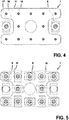
- shows the top view of the power semiconductor module of
Fig. 1 without its housing, - Fig. 5
- shows a bottom view of the arrangement of
Fig. 4 , and - Fig. 6
- shows another sectional view along the line G-G of the power semiconductor module shown in
Fig. 1 with the top plate. -
Fig. 1 shows a top view of apower semiconductor module 1 according to the present invention. Thepower semiconductor module 1 comprises, as best seen inFigs. 2 and3 as well as inFig. 6 , abase plate 2 and multiplepower semiconductor devices 3. Thepower semiconductor devices 3 in this embodiment of the invention are power transistors like IGBTs and - power diodes, which are commonly arranged on the
base plate 2. Thepower semiconductor devices 3 are on their bottom face in surface contact with thebase plate 2 to provide mechanical connection as well as electrical and thermal conductivity there between. For the IGBTs,gate runners 4 are provided on thebase plate 2.Gate runners 4 are electric contact plates isolated from thebase plate 2 and commonly connected to the gates of the IGBTs. - The
gate runner 4 is contacted by afirst presspin 5, also referred to as gate pin, which is a presspin known in the art and therefore not described in detail. Thepower semiconductor devices 3 are further contacted on their top face via anintermediate contact element 6, which is here shown as two-layer contact element 6, bysecond presspins 7, which are also referred to as chip pins. The chip pins 7 have an essentially inverse structure compared to the gate pins 5 and comprise afoot 8 with a throughhole 9 and ashaft 10, which is moveable within the throughhole 9. Aprotection plate 11 integrally forms a common head of the chip pins 7. The chip pins 7 further comprise thespring washer pack 12, which is arranged around theshaft 10 between theprotection plate 11 and thefoot 8 for exerting an outwardly directed force on theprotection plate 11 and thefoot 8, and acurrent bypass 13, which electrically connects thefoot 8 and theprotection plate 11. - For mounting the chip pins 7, the
protection plate 11 is provided with several throughholes 14, in which anupper end region 15 of theshaft 10 is received. The through holes 14 and theupper end regions 15 of theshafts 10 are provided with a corresponding thread, so that theshafts 10 are fixed to theprotection plate 11 by means of a thread connection. In an alternative embodiment, theshafts 10 are press-fitted into the through holes 14. - In an example not forming part of the present invention but useful for understanding it, the
protection plate 11 and thebase plate 2 are made of molybdenum. Theprotection plate 11 is provided below atop plate 20, which is shown inFig. 6 , and covers the inner face of thetop plate 20. Theprotection plate 11 is in electrical contact with thetop plate 20. Theprotection plate 11 is provided with a number ofgaps 16, which surround heads 17 of the gate pins 5. The gate pins 5 with theirheads 17 are in mechanical contact with thetop plate 20, whereby isolation means are provided between thehead 17 and the top plate. - The
power semiconductor module 1 comprises ahousing 18, whereby thebase plate 2 forms a base of thehousing 18. The electrically conductingtop plate 20 forms a top side of thehousing 18. The top plate provides a first contact of thepower semiconductor module 1 and thebase plate 2 provides a second contact of thepower semiconductor module 1. Thepower semiconductor devices 3 are in mechanical and electrical contact with the top plate by means of thepresspins protection plate 11, whereby the gate pins 5 are electrically isolated from thetop plate 20. Thebase plate 2 is connected to the collectors, i.e. second contacts of thepower semiconductor devices 3 and forms a second contact of thepower semiconductor module 1, and the emitters, i.e. first contacts of thepower semiconductor devices 3 are connected to the top plate. The gates of thepower semiconductor devices 3 can be commonly contacted in thepower semiconductor module 1 through a gap in the top plate or be provided by agate conductor 21 provided at thetop plate 20 and insulated from it on the side towards thebase plate 2. - A power semiconductor module assembly, which is not explicitly shown in the figures, comprises multiple
power semiconductor modules 1 as described above. Thepower semiconductor modules 1 are arranged side by side to each other within a housing, whereby thebase plates 2 of thepower semiconductor modules 1 extend through a base of the housing. An electrically conducting lid forms a top side of the housing and provides a common contact for thepower semiconductor modules 1 with electric connections between adjacentpower semiconductor modules 1. The lid provides a first contact of the power semiconductor module assembly for contacting the first contacts of thepower semiconductor modules 1 and thebase plates 2 commonly provide a second contact of the power semiconductor module assembly. Alternatively the lid of the power semiconductor module assembly forms a common lid or a commontop plate 20 for the modules arranged in the assembly. The control contacts of thepower semiconductor modules 1 are connected to each other within the power semiconductor module assembly and to a lateral electric contact of the power semiconductor module assembly. - The
power semiconductor modules 1 as well as the power semiconductor module assemblies can be stacked, with coolers arranged between neighboringpower semiconductor modules 1 or power semiconductor module assemblies. - While the invention has been illustrated and described in detail in the drawings and foregoing description, such illustration and description are to be considered illustrative or exemplary and not restrictive; the invention is not limited to the disclosed embodiments. Other variations to be disclosed embodiments can be understood and effected by those skilled in the art in practicing the claimed invention, from a study of the drawings, the disclosure, and the appended claims. In the claims, the word "comprising" does not exclude other elements or steps, and the indefinite article "a" or "an" does not exclude a plurality. The mere fact that certain measures are recited in mutually different dependent claims does not indicate that a combination of these measures cannot be used to advantage. Any reference signs in the claims should not be construed as limiting scope.
- Reference signs list
- 1
- power semiconductor module
- 2
- base plate
- 3
- power semiconductor device
- 4
- gate runner
- 5
- first presspin, gate pin
- 6
- contact element
- 7
- second presspin, chip pin
- 8
- foot
- 9
- through hole
- 10
- shaft
- 11
- protection plate
- 12
- spring washer pack
- 13
- current bypass
- 14
- through hole
- 15
- upper end region
- 16
- gap
- 17
- head
- 18
- housing
- 20
- top plate, lid
- 21
- gate conductor
Claims (10)
- Power semiconductor module (1) comprisingan electrically conducting base plate (2),an electrically conducting top plate (20), arranged in parallel to the base plate (2) and spaced apart from the base plate (2),at least one power semiconductor device (3), which is arranged on the base plate (2) in a space formed between the base plate (2) and the top plate, andat least one presspin (5, 7), which is arranged in the space formed between the base plate (2) and the top plate (20) to provide contact between the power semiconductor device (3) and the top plate,characterized in thata metallic protection plate (11) is provided at an inner face of the top plate facing towards the base plate (2), whereby the material of the protection plate (11) has a melting temperature higher than the melting temperature of the top plate (20), and wherein the material of the protection plate (11) is an alloy comprising molybdenum and copper.
- Power semiconductor module (1) according to any preceding claim, characterized in that
the protection plate (11) covers the surface of the top plate in the area of a head (17) of the at least one presspin (7). - Power semiconductor module (1) according to any preceding claim 1 to 2,
characterized in that
the protection plate (11) is provided with at least one gap (16) which is positioned to surround a head (17) of the at least one presspin (5). - Power semiconductor module (1) according to any preceding claim,
characterized in that
the protection plate (11) is provided integral with the head of the at least one presspin (7). - Power semiconductor module (1) according to preceding claim 4, characterized in that
the least one presspin (7) has a structure with its shaft (10) fixed to its head and its foot movable (8) along its shaft (10). - Power semiconductor module (1) according to any preceding claim,
characterized in that
the at least one power semiconductor device (3) is an insulated gate bipolar transistor, a reverse conducting insulated gate bipolar transistor, a bi-mode insulated gate transistor, or a diode. - Power semiconductor module (1) according to any preceding claim,
characterized in that
the power semiconductor module (1) comprises a housing (18), wherebythe top plate forms a top side of the housing (18) and provides a first contact of the power semiconductor module (1),the base plate (2) forms a base of the housing (18) and provides a second contact of the power semiconductor module (1). - Power semiconductor module assembly, comprising multiple power semiconductor modules (1) according to any of preceding claims 1 to 7, whereby
the power semiconductor modules (1) are arranged side by side to each other with electric connections between adjacent power semiconductor modules (1). - Power semiconductor module assembly according to preceding claim 8, characterized in that
the base plates (2) of the power semiconductor modules (1) are electrically connected to each other. - Power semiconductor module assembly according to any of preceding 8 or 9, characterized in thatthe power semiconductor module assembly comprises a housing, whereby an electrically conducting lid forms a top side of the housing and provides a first contact of the power semiconductor module assembly, which is in contact with the first contacts of the power semiconductor modules (1), andthe base plates (2) of the power semiconductor modules (1) extend through a base of the housing.
Priority Applications (1)
| Application Number | Priority Date | Filing Date | Title |
|---|---|---|---|
| EP12772970.5A EP2769410B8 (en) | 2011-10-21 | 2012-10-18 | Power semiconductor module and power semiconductor module assembly with multiple power semiconductor modules |
Applications Claiming Priority (3)
| Application Number | Priority Date | Filing Date | Title |
|---|---|---|---|
| EP11186101 | 2011-10-21 | ||
| PCT/EP2012/070621 WO2013057172A1 (en) | 2011-10-21 | 2012-10-18 | Power semiconducter module and power semiconductor module assembly with multiple power semiconducter modules |
| EP12772970.5A EP2769410B8 (en) | 2011-10-21 | 2012-10-18 | Power semiconductor module and power semiconductor module assembly with multiple power semiconductor modules |
Publications (3)
| Publication Number | Publication Date |
|---|---|
| EP2769410A1 EP2769410A1 (en) | 2014-08-27 |
| EP2769410B1 true EP2769410B1 (en) | 2021-12-01 |
| EP2769410B8 EP2769410B8 (en) | 2022-01-05 |
Family
ID=47022706
Family Applications (1)
| Application Number | Title | Priority Date | Filing Date |
|---|---|---|---|
| EP12772970.5A Active EP2769410B8 (en) | 2011-10-21 | 2012-10-18 | Power semiconductor module and power semiconductor module assembly with multiple power semiconductor modules |
Country Status (6)
| Country | Link |
|---|---|
| US (1) | US9035447B2 (en) |
| EP (1) | EP2769410B8 (en) |
| JP (1) | JP6109181B2 (en) |
| KR (1) | KR101871026B1 (en) |
| CN (1) | CN103890941B (en) |
| WO (1) | WO2013057172A1 (en) |
Families Citing this family (13)
| Publication number | Priority date | Publication date | Assignee | Title |
|---|---|---|---|---|
| EP3168873A1 (en) | 2015-11-11 | 2017-05-17 | ABB Technology AG | Power semiconductor module |
| DE112016007203B4 (en) | 2016-09-07 | 2025-07-17 | Mitsubishi Electric Corporation | semiconductor device |
| EP3352213B1 (en) * | 2017-01-23 | 2021-10-06 | ABB Power Grids Switzerland AG | Semiconductor power module comprising graphene |
| WO2018141811A1 (en) * | 2017-02-01 | 2018-08-09 | Abb Schweiz Ag | Power semiconductor device with active short circuit failure mode |
| CN110148574B (en) * | 2019-05-21 | 2024-12-13 | 全球能源互联网研究院有限公司 | Chip pressing structure and semiconductor packaging structure |
| CN110416194B (en) * | 2019-06-11 | 2025-08-22 | 全球能源互联网研究院有限公司 | An insulating frame structure for press-fit IGBT |
| CN110828433A (en) * | 2019-09-30 | 2020-02-21 | 全球能源互联网研究院有限公司 | An elastic crimping package structure |
| CN112992866A (en) * | 2019-12-18 | 2021-06-18 | 株洲中车时代半导体有限公司 | Current bypass structure and IGBT device |
| WO2021220351A1 (en) * | 2020-04-27 | 2021-11-04 | 三菱電機株式会社 | Electrical conduction structure and power semiconductor module |
| CN112636054B (en) * | 2020-11-27 | 2022-08-05 | 株洲中车时代半导体有限公司 | Semiconductor device assembly, pressure-contact power semiconductor module and manufacturing method |
| CN112490724B (en) * | 2020-11-27 | 2023-02-03 | 株洲中车时代半导体有限公司 | Disc spring assembly and power semiconductor module |
| US12587188B2 (en) * | 2022-03-01 | 2026-03-24 | Nutech Ventures | Power modules for circuit protection |
| EP4704147A1 (en) * | 2024-08-29 | 2026-03-04 | Hitachi Energy Ltd | Power semiconductor module and method for creating a current bypass in the power semiconductor module |
Citations (1)
| Publication number | Priority date | Publication date | Assignee | Title |
|---|---|---|---|---|
| FR2813440A1 (en) * | 2000-08-30 | 2002-03-01 | Mitsubishi Electric Corp | SEMICONDUCTOR DEVICE FOR DRIVING ELECTRICAL ENERGY |
Family Cites Families (24)
| Publication number | Priority date | Publication date | Assignee | Title |
|---|---|---|---|---|
| BE623873A (en) * | 1961-10-24 | 1900-01-01 | ||
| US4950554A (en) * | 1989-05-30 | 1990-08-21 | Amax Inc. | Composite copper-molybdenum sheet |
| DE59107655D1 (en) * | 1991-02-22 | 1996-05-09 | Asea Brown Boveri | High-performance semiconductor component that can be switched off |
| US5705873A (en) | 1993-12-22 | 1998-01-06 | Canon Denshi Kabushiki Kaisha | Light-quantity control device |
| DE19530264A1 (en) * | 1995-08-17 | 1997-02-20 | Abb Management Ag | Power semiconductor module |
| JPH09275186A (en) * | 1996-04-02 | 1997-10-21 | Fuji Electric Co Ltd | Semiconductor device |
| GB9725960D0 (en) | 1997-12-08 | 1998-02-04 | Westinghouse Brake & Signal | Encapsulating semiconductor chips |
| JP3617306B2 (en) * | 1998-04-15 | 2005-02-02 | 株式会社日立製作所 | Pressurized contact semiconductor device and converter using the same |
| DE19843309A1 (en) * | 1998-09-22 | 2000-03-23 | Asea Brown Boveri | Short-circuit proof IGBT module |
| JP3730428B2 (en) * | 1998-12-22 | 2006-01-05 | 富士通株式会社 | Manufacturing method of contactor for semiconductor device test |
| DE19903245A1 (en) * | 1999-01-27 | 2000-08-03 | Asea Brown Boveri | Power semiconductor module |
| JP2001036002A (en) * | 1999-07-23 | 2001-02-09 | Fuji Electric Co Ltd | Semiconductor device |
| EP1209742A1 (en) | 2000-11-22 | 2002-05-29 | ABB Schweiz AG | Power Semiconductor Module and application of such a Power Semiconductor Module |
| US20020074640A1 (en) * | 2000-12-20 | 2002-06-20 | Gamboa Rodolfo I. | Semiconductor test socket having pogo-pin contacts |
| EP1263046A1 (en) * | 2001-06-01 | 2002-12-04 | ABB Schweiz AG | Contact Arrangement |
| EP1263045A1 (en) * | 2001-06-01 | 2002-12-04 | ABB Schweiz AG | High power semiconductor module |
| EP1291914A1 (en) * | 2001-09-10 | 2003-03-12 | ABB Schweiz AG | Pressure-contactable power semiconductor module |
| JP3741995B2 (en) * | 2001-10-31 | 2006-02-01 | 株式会社ルネサステクノロジ | Device and method for removing tie bar after resin sealing of semiconductor device, and method for manufacturing semiconductor device |
| US6654250B1 (en) * | 2002-09-25 | 2003-11-25 | International Business Machines Corporation | Low-stress compressive heatsink structure |
| EP1403923A1 (en) * | 2002-09-27 | 2004-03-31 | Abb Research Ltd. | Press pack power semiconductor module |
| EP1475832A1 (en) * | 2003-05-05 | 2004-11-10 | ABB Technology AG | Pressure-contactable power semiconductor module |
| JP5253161B2 (en) * | 2006-06-07 | 2013-07-31 | 三菱電機株式会社 | Thermal resistor and semiconductor device and electrical device using the same |
| CN101231981A (en) * | 2007-01-24 | 2008-07-30 | 贵阳华翔半导体有限公司 | Structural Improvement of Lead Frame for Semiconductor Die Packaging |
| DE102010003367B4 (en) * | 2010-03-26 | 2015-06-25 | Infineon Technologies Ag | Press-fit connections for electronic modules |
-
2012
- 2012-10-18 EP EP12772970.5A patent/EP2769410B8/en active Active
- 2012-10-18 WO PCT/EP2012/070621 patent/WO2013057172A1/en not_active Ceased
- 2012-10-18 KR KR1020147010506A patent/KR101871026B1/en active Active
- 2012-10-18 CN CN201280051153.8A patent/CN103890941B/en active Active
- 2012-10-18 JP JP2014536228A patent/JP6109181B2/en active Active
-
2014
- 2014-04-21 US US14/257,397 patent/US9035447B2/en active Active
Patent Citations (1)
| Publication number | Priority date | Publication date | Assignee | Title |
|---|---|---|---|---|
| FR2813440A1 (en) * | 2000-08-30 | 2002-03-01 | Mitsubishi Electric Corp | SEMICONDUCTOR DEVICE FOR DRIVING ELECTRICAL ENERGY |
Also Published As
| Publication number | Publication date |
|---|---|
| KR101871026B1 (en) | 2018-06-25 |
| US20140225245A1 (en) | 2014-08-14 |
| CN103890941A (en) | 2014-06-25 |
| KR20140085455A (en) | 2014-07-07 |
| EP2769410B8 (en) | 2022-01-05 |
| CN103890941B (en) | 2016-10-26 |
| JP6109181B2 (en) | 2017-04-05 |
| JP2014531133A (en) | 2014-11-20 |
| EP2769410A1 (en) | 2014-08-27 |
| WO2013057172A1 (en) | 2013-04-25 |
| US9035447B2 (en) | 2015-05-19 |
Similar Documents
| Publication | Publication Date | Title |
|---|---|---|
| US9035447B2 (en) | Power semiconductor module and power semiconductor module assembly with multiple power semiconductor modules | |
| US10867980B2 (en) | Semiconductor equipment | |
| KR101375502B1 (en) | Power semiconductor module | |
| EP2560204A2 (en) | Power semiconducter module and semiconducter module assembly with multiple power semiconducter modules | |
| CN115241142B (en) | Semiconductor power modules including graphene | |
| CN103650137A (en) | Power semiconductor module | |
| JP2017162991A (en) | Switching element | |
| US20170236819A1 (en) | Semiconductor device and manufacturing method | |
| JP2013033812A (en) | Power semiconductor module | |
| KR102853786B1 (en) | Solid state circuit breaker(sscb) | |
| US20150138733A1 (en) | Semiconductor device | |
| CN100533764C (en) | Semiconductor device module structure | |
| JP4984485B2 (en) | Semiconductor device | |
| CN110892524A (en) | Bypass thyristor device with gas expansion chamber in contact plate | |
| US20130043579A1 (en) | Power semiconductor arrangement, power semiconductor module with multiple power semiconductor arrangements, and module assembly comprising multiple power semiconductor modules | |
| US20190189538A1 (en) | Semiconductor device | |
| EP2660863B1 (en) | Power semiconductor module | |
| EP2827366A1 (en) | Power semiconductor module | |
| JP2020136315A (en) | Semiconductor device | |
| EP2966681A1 (en) | Power semiconductor devices | |
| US11456736B2 (en) | Circuit arrangement, power converter module, and method for operating the power converter module | |
| EP3751600A1 (en) | Semiconductor device | |
| KR102564865B1 (en) | Thermoelectonic module | |
| CN216015420U (en) | Thermoelectric refrigerator and electronic equipment with same | |
| JP5817696B2 (en) | Semiconductor device |
Legal Events
| Date | Code | Title | Description |
|---|---|---|---|
| PUAI | Public reference made under article 153(3) epc to a published international application that has entered the european phase |
Free format text: ORIGINAL CODE: 0009012 |
|
| 17P | Request for examination filed |
Effective date: 20140401 |
|
| AK | Designated contracting states |
Kind code of ref document: A1 Designated state(s): AL AT BE BG CH CY CZ DE DK EE ES FI FR GB GR HR HU IE IS IT LI LT LU LV MC MK MT NL NO PL PT RO RS SE SI SK SM TR |
|
| DAX | Request for extension of the european patent (deleted) | ||
| RAP1 | Party data changed (applicant data changed or rights of an application transferred) |
Owner name: ABB SCHWEIZ AG |
|
| STAA | Information on the status of an ep patent application or granted ep patent |
Free format text: STATUS: EXAMINATION IS IN PROGRESS |
|
| 17Q | First examination report despatched |
Effective date: 20190508 |
|
| RAP1 | Party data changed (applicant data changed or rights of an application transferred) |
Owner name: ABB POWER GRIDS SWITZERLAND AG |
|
| RIC1 | Information provided on ipc code assigned before grant |
Ipc: H01L 25/07 20060101AFI20210422BHEP Ipc: H01L 23/051 20060101ALI20210422BHEP Ipc: H01L 23/48 20060101ALI20210422BHEP Ipc: H01L 23/62 20060101ALI20210422BHEP Ipc: H01L 23/492 20060101ALI20210422BHEP Ipc: H01L 23/00 20060101ALI20210422BHEP |
|
| GRAP | Despatch of communication of intention to grant a patent |
Free format text: ORIGINAL CODE: EPIDOSNIGR1 |
|
| STAA | Information on the status of an ep patent application or granted ep patent |
Free format text: STATUS: GRANT OF PATENT IS INTENDED |
|
| INTG | Intention to grant announced |
Effective date: 20210614 |
|
| GRAS | Grant fee paid |
Free format text: ORIGINAL CODE: EPIDOSNIGR3 |
|
| GRAA | (expected) grant |
Free format text: ORIGINAL CODE: 0009210 |
|
| STAA | Information on the status of an ep patent application or granted ep patent |
Free format text: STATUS: THE PATENT HAS BEEN GRANTED |
|
| GRAT | Correction requested after decision to grant or after decision to maintain patent in amended form |
Free format text: ORIGINAL CODE: EPIDOSNCDEC |
|
| REG | Reference to a national code |
Ref country code: DE Ref legal event code: R081 Ref document number: 602012077278 Country of ref document: DE Owner name: HITACHI ENERGY LTD, CH Free format text: FORMER OWNER: ABB POWER GRIDS SWITZERLAND AG, BADEN, CH |
|
| RIN1 | Information on inventor provided before grant (corrected) |
Inventor name: TRUESSEL, DOMINIK Inventor name: DUGAL, FRANC |
|
| AK | Designated contracting states |
Kind code of ref document: B1 Designated state(s): AL AT BE BG CH CY CZ DE DK EE ES FI FR GB GR HR HU IE IS IT LI LT LU LV MC MK MT NL NO PL PT RO RS SE SI SK SM TR |
|
| REG | Reference to a national code |
Ref country code: GB Ref legal event code: FG4D |
|
| RAP4 | Party data changed (patent owner data changed or rights of a patent transferred) |
Owner name: HITACHI ENERGY SWITZERLAND AG |
|
| REG | Reference to a national code |
Ref country code: AT Ref legal event code: REF Ref document number: 1452620 Country of ref document: AT Kind code of ref document: T Effective date: 20211215 Ref country code: CH Ref legal event code: PK Free format text: BERICHTIGUNG B8 Ref country code: CH Ref legal event code: EP |
|
| REG | Reference to a national code |
Ref country code: IE Ref legal event code: FG4D |
|
| REG | Reference to a national code |
Ref country code: DE Ref legal event code: R096 Ref document number: 602012077278 Country of ref document: DE |
|
| REG | Reference to a national code |
Ref country code: LT Ref legal event code: MG9D |
|
| REG | Reference to a national code |
Ref country code: NL Ref legal event code: MP Effective date: 20211201 |
|
| REG | Reference to a national code |
Ref country code: AT Ref legal event code: MK05 Ref document number: 1452620 Country of ref document: AT Kind code of ref document: T Effective date: 20211201 |
|
| PG25 | Lapsed in a contracting state [announced via postgrant information from national office to epo] |
Ref country code: RS Free format text: LAPSE BECAUSE OF FAILURE TO SUBMIT A TRANSLATION OF THE DESCRIPTION OR TO PAY THE FEE WITHIN THE PRESCRIBED TIME-LIMIT Effective date: 20211201 Ref country code: LT Free format text: LAPSE BECAUSE OF FAILURE TO SUBMIT A TRANSLATION OF THE DESCRIPTION OR TO PAY THE FEE WITHIN THE PRESCRIBED TIME-LIMIT Effective date: 20211201 Ref country code: FI Free format text: LAPSE BECAUSE OF FAILURE TO SUBMIT A TRANSLATION OF THE DESCRIPTION OR TO PAY THE FEE WITHIN THE PRESCRIBED TIME-LIMIT Effective date: 20211201 Ref country code: BG Free format text: LAPSE BECAUSE OF FAILURE TO SUBMIT A TRANSLATION OF THE DESCRIPTION OR TO PAY THE FEE WITHIN THE PRESCRIBED TIME-LIMIT Effective date: 20220301 Ref country code: AT Free format text: LAPSE BECAUSE OF FAILURE TO SUBMIT A TRANSLATION OF THE DESCRIPTION OR TO PAY THE FEE WITHIN THE PRESCRIBED TIME-LIMIT Effective date: 20211201 |
|
| PG25 | Lapsed in a contracting state [announced via postgrant information from national office to epo] |
Ref country code: SK Free format text: LAPSE BECAUSE OF FAILURE TO SUBMIT A TRANSLATION OF THE DESCRIPTION OR TO PAY THE FEE WITHIN THE PRESCRIBED TIME-LIMIT Effective date: 20211201 Ref country code: SE Free format text: LAPSE BECAUSE OF FAILURE TO SUBMIT A TRANSLATION OF THE DESCRIPTION OR TO PAY THE FEE WITHIN THE PRESCRIBED TIME-LIMIT Effective date: 20211201 Ref country code: PL Free format text: LAPSE BECAUSE OF FAILURE TO SUBMIT A TRANSLATION OF THE DESCRIPTION OR TO PAY THE FEE WITHIN THE PRESCRIBED TIME-LIMIT Effective date: 20211201 Ref country code: NO Free format text: LAPSE BECAUSE OF FAILURE TO SUBMIT A TRANSLATION OF THE DESCRIPTION OR TO PAY THE FEE WITHIN THE PRESCRIBED TIME-LIMIT Effective date: 20220301 Ref country code: LV Free format text: LAPSE BECAUSE OF FAILURE TO SUBMIT A TRANSLATION OF THE DESCRIPTION OR TO PAY THE FEE WITHIN THE PRESCRIBED TIME-LIMIT Effective date: 20211201 Ref country code: HR Free format text: LAPSE BECAUSE OF FAILURE TO SUBMIT A TRANSLATION OF THE DESCRIPTION OR TO PAY THE FEE WITHIN THE PRESCRIBED TIME-LIMIT Effective date: 20211201 Ref country code: GR Free format text: LAPSE BECAUSE OF FAILURE TO SUBMIT A TRANSLATION OF THE DESCRIPTION OR TO PAY THE FEE WITHIN THE PRESCRIBED TIME-LIMIT Effective date: 20220302 Ref country code: ES Free format text: LAPSE BECAUSE OF FAILURE TO SUBMIT A TRANSLATION OF THE DESCRIPTION OR TO PAY THE FEE WITHIN THE PRESCRIBED TIME-LIMIT Effective date: 20211201 |
|
| PG25 | Lapsed in a contracting state [announced via postgrant information from national office to epo] |
Ref country code: NL Free format text: LAPSE BECAUSE OF FAILURE TO SUBMIT A TRANSLATION OF THE DESCRIPTION OR TO PAY THE FEE WITHIN THE PRESCRIBED TIME-LIMIT Effective date: 20211201 |
|
| PG25 | Lapsed in a contracting state [announced via postgrant information from national office to epo] |
Ref country code: SM Free format text: LAPSE BECAUSE OF FAILURE TO SUBMIT A TRANSLATION OF THE DESCRIPTION OR TO PAY THE FEE WITHIN THE PRESCRIBED TIME-LIMIT Effective date: 20211201 Ref country code: RO Free format text: LAPSE BECAUSE OF FAILURE TO SUBMIT A TRANSLATION OF THE DESCRIPTION OR TO PAY THE FEE WITHIN THE PRESCRIBED TIME-LIMIT Effective date: 20211201 Ref country code: PT Free format text: LAPSE BECAUSE OF FAILURE TO SUBMIT A TRANSLATION OF THE DESCRIPTION OR TO PAY THE FEE WITHIN THE PRESCRIBED TIME-LIMIT Effective date: 20220401 Ref country code: EE Free format text: LAPSE BECAUSE OF FAILURE TO SUBMIT A TRANSLATION OF THE DESCRIPTION OR TO PAY THE FEE WITHIN THE PRESCRIBED TIME-LIMIT Effective date: 20211201 Ref country code: CZ Free format text: LAPSE BECAUSE OF FAILURE TO SUBMIT A TRANSLATION OF THE DESCRIPTION OR TO PAY THE FEE WITHIN THE PRESCRIBED TIME-LIMIT Effective date: 20211201 |
|
| REG | Reference to a national code |
Ref country code: DE Ref legal event code: R097 Ref document number: 602012077278 Country of ref document: DE |
|
| PG25 | Lapsed in a contracting state [announced via postgrant information from national office to epo] |
Ref country code: IS Free format text: LAPSE BECAUSE OF FAILURE TO SUBMIT A TRANSLATION OF THE DESCRIPTION OR TO PAY THE FEE WITHIN THE PRESCRIBED TIME-LIMIT Effective date: 20220401 |
|
| PLBE | No opposition filed within time limit |
Free format text: ORIGINAL CODE: 0009261 |
|
| STAA | Information on the status of an ep patent application or granted ep patent |
Free format text: STATUS: NO OPPOSITION FILED WITHIN TIME LIMIT |
|
| PG25 | Lapsed in a contracting state [announced via postgrant information from national office to epo] |
Ref country code: DK Free format text: LAPSE BECAUSE OF FAILURE TO SUBMIT A TRANSLATION OF THE DESCRIPTION OR TO PAY THE FEE WITHIN THE PRESCRIBED TIME-LIMIT Effective date: 20211201 Ref country code: AL Free format text: LAPSE BECAUSE OF FAILURE TO SUBMIT A TRANSLATION OF THE DESCRIPTION OR TO PAY THE FEE WITHIN THE PRESCRIBED TIME-LIMIT Effective date: 20211201 |
|
| 26N | No opposition filed |
Effective date: 20220902 |
|
| PG25 | Lapsed in a contracting state [announced via postgrant information from national office to epo] |
Ref country code: SI Free format text: LAPSE BECAUSE OF FAILURE TO SUBMIT A TRANSLATION OF THE DESCRIPTION OR TO PAY THE FEE WITHIN THE PRESCRIBED TIME-LIMIT Effective date: 20211201 |
|
| PG25 | Lapsed in a contracting state [announced via postgrant information from national office to epo] |
Ref country code: MC Free format text: LAPSE BECAUSE OF FAILURE TO SUBMIT A TRANSLATION OF THE DESCRIPTION OR TO PAY THE FEE WITHIN THE PRESCRIBED TIME-LIMIT Effective date: 20211201 Ref country code: IT Free format text: LAPSE BECAUSE OF FAILURE TO SUBMIT A TRANSLATION OF THE DESCRIPTION OR TO PAY THE FEE WITHIN THE PRESCRIBED TIME-LIMIT Effective date: 20211201 |
|
| REG | Reference to a national code |
Ref country code: CH Ref legal event code: PL |
|
| REG | Reference to a national code |
Ref country code: BE Ref legal event code: MM Effective date: 20221031 |
|
| PG25 | Lapsed in a contracting state [announced via postgrant information from national office to epo] |
Ref country code: LU Free format text: LAPSE BECAUSE OF NON-PAYMENT OF DUE FEES Effective date: 20221018 |
|
| P01 | Opt-out of the competence of the unified patent court (upc) registered |
Effective date: 20230527 |
|
| PG25 | Lapsed in a contracting state [announced via postgrant information from national office to epo] |
Ref country code: LI Free format text: LAPSE BECAUSE OF NON-PAYMENT OF DUE FEES Effective date: 20221031 Ref country code: FR Free format text: LAPSE BECAUSE OF NON-PAYMENT OF DUE FEES Effective date: 20221031 Ref country code: CH Free format text: LAPSE BECAUSE OF NON-PAYMENT OF DUE FEES Effective date: 20221031 |
|
| PG25 | Lapsed in a contracting state [announced via postgrant information from national office to epo] |
Ref country code: BE Free format text: LAPSE BECAUSE OF NON-PAYMENT OF DUE FEES Effective date: 20221031 |
|
| PG25 | Lapsed in a contracting state [announced via postgrant information from national office to epo] |
Ref country code: IE Free format text: LAPSE BECAUSE OF NON-PAYMENT OF DUE FEES Effective date: 20221018 |
|
| PG25 | Lapsed in a contracting state [announced via postgrant information from national office to epo] |
Ref country code: HU Free format text: LAPSE BECAUSE OF FAILURE TO SUBMIT A TRANSLATION OF THE DESCRIPTION OR TO PAY THE FEE WITHIN THE PRESCRIBED TIME-LIMIT; INVALID AB INITIO Effective date: 20121018 |
|
| REG | Reference to a national code |
Ref country code: DE Ref legal event code: R081 Ref document number: 602012077278 Country of ref document: DE Owner name: HITACHI ENERGY LTD, CH Free format text: FORMER OWNER: HITACHI ENERGY SWITZERLAND AG, BADEN, CH |
|
| PG25 | Lapsed in a contracting state [announced via postgrant information from national office to epo] |
Ref country code: CY Free format text: LAPSE BECAUSE OF FAILURE TO SUBMIT A TRANSLATION OF THE DESCRIPTION OR TO PAY THE FEE WITHIN THE PRESCRIBED TIME-LIMIT Effective date: 20211201 |
|
| PG25 | Lapsed in a contracting state [announced via postgrant information from national office to epo] |
Ref country code: MK Free format text: LAPSE BECAUSE OF FAILURE TO SUBMIT A TRANSLATION OF THE DESCRIPTION OR TO PAY THE FEE WITHIN THE PRESCRIBED TIME-LIMIT Effective date: 20211201 |
|
| REG | Reference to a national code |
Ref country code: GB Ref legal event code: 732E Free format text: REGISTERED BETWEEN 20240718 AND 20240724 |
|
| PG25 | Lapsed in a contracting state [announced via postgrant information from national office to epo] |
Ref country code: MT Free format text: LAPSE BECAUSE OF FAILURE TO SUBMIT A TRANSLATION OF THE DESCRIPTION OR TO PAY THE FEE WITHIN THE PRESCRIBED TIME-LIMIT Effective date: 20211201 |
|
| REG | Reference to a national code |
Ref country code: DE Ref legal event code: R079 Ref document number: 602012077278 Country of ref document: DE Free format text: PREVIOUS MAIN CLASS: H01L0025070000 Ipc: H10D0080200000 |
|
| REG | Reference to a national code |
Ref country code: DE Ref legal event code: R082 Ref document number: 602012077278 Country of ref document: DE Representative=s name: DENNEMEYER & ASSOCIATES RECHTSANWALTSGESELLSCH, DE |
|
| PG25 | Lapsed in a contracting state [announced via postgrant information from national office to epo] |
Ref country code: TR Free format text: LAPSE BECAUSE OF FAILURE TO SUBMIT A TRANSLATION OF THE DESCRIPTION OR TO PAY THE FEE WITHIN THE PRESCRIBED TIME-LIMIT Effective date: 20211201 |
|
| PGFP | Annual fee paid to national office [announced via postgrant information from national office to epo] |
Ref country code: DE Payment date: 20251021 Year of fee payment: 14 |
|
| PGFP | Annual fee paid to national office [announced via postgrant information from national office to epo] |
Ref country code: GB Payment date: 20251022 Year of fee payment: 14 |