EP2765700A1 - Power converter - Google Patents
Power converter Download PDFInfo
- Publication number
- EP2765700A1 EP2765700A1 EP12838013.6A EP12838013A EP2765700A1 EP 2765700 A1 EP2765700 A1 EP 2765700A1 EP 12838013 A EP12838013 A EP 12838013A EP 2765700 A1 EP2765700 A1 EP 2765700A1
- Authority
- EP
- European Patent Office
- Prior art keywords
- bidirectional switching
- switching elements
- power converter
- power
- phase
- Prior art date
- Legal status (The legal status is an assumption and is not a legal conclusion. Google has not performed a legal analysis and makes no representation as to the accuracy of the status listed.)
- Granted
Links
- 230000002457 bidirectional effect Effects 0.000 claims abstract description 110
- 239000003990 capacitor Substances 0.000 claims abstract description 75
- 238000006243 chemical reaction Methods 0.000 claims abstract description 23
- 230000000694 effects Effects 0.000 description 6
- 239000011159 matrix material Substances 0.000 description 6
- 230000002500 effect on skin Effects 0.000 description 4
- 238000009499 grossing Methods 0.000 description 4
- 239000004020 conductor Substances 0.000 description 2
- 238000010586 diagram Methods 0.000 description 2
- RYGMFSIKBFXOCR-UHFFFAOYSA-N Copper Chemical compound [Cu] RYGMFSIKBFXOCR-UHFFFAOYSA-N 0.000 description 1
- 230000000903 blocking effect Effects 0.000 description 1
- 229910052802 copper Inorganic materials 0.000 description 1
- 239000010949 copper Substances 0.000 description 1
- 238000012986 modification Methods 0.000 description 1
- 230000004048 modification Effects 0.000 description 1
- 230000001105 regulatory effect Effects 0.000 description 1
- 239000004065 semiconductor Substances 0.000 description 1
- 238000011144 upstream manufacturing Methods 0.000 description 1
Images



Classifications
-
- H—ELECTRICITY
- H02—GENERATION; CONVERSION OR DISTRIBUTION OF ELECTRIC POWER
- H02M—APPARATUS FOR CONVERSION BETWEEN AC AND AC, BETWEEN AC AND DC, OR BETWEEN DC AND DC, AND FOR USE WITH MAINS OR SIMILAR POWER SUPPLY SYSTEMS; CONVERSION OF DC OR AC INPUT POWER INTO SURGE OUTPUT POWER; CONTROL OR REGULATION THEREOF
- H02M5/00—Conversion of AC power input into AC power output, e.g. for change of voltage, for change of frequency, for change of number of phases
- H02M5/02—Conversion of AC power input into AC power output, e.g. for change of voltage, for change of frequency, for change of number of phases without intermediate conversion into DC
- H02M5/04—Conversion of AC power input into AC power output, e.g. for change of voltage, for change of frequency, for change of number of phases without intermediate conversion into DC by static converters
- H02M5/22—Conversion of AC power input into AC power output, e.g. for change of voltage, for change of frequency, for change of number of phases without intermediate conversion into DC by static converters using discharge tubes with control electrode or semiconductor devices with control electrode
- H02M5/275—Conversion of AC power input into AC power output, e.g. for change of voltage, for change of frequency, for change of number of phases without intermediate conversion into DC by static converters using discharge tubes with control electrode or semiconductor devices with control electrode using devices of a triode or transistor type requiring continuous application of a control signal
- H02M5/297—Conversion of AC power input into AC power output, e.g. for change of voltage, for change of frequency, for change of number of phases without intermediate conversion into DC by static converters using discharge tubes with control electrode or semiconductor devices with control electrode using devices of a triode or transistor type requiring continuous application of a control signal for conversion of frequency
-
- H—ELECTRICITY
- H02—GENERATION; CONVERSION OR DISTRIBUTION OF ELECTRIC POWER
- H02M—APPARATUS FOR CONVERSION BETWEEN AC AND AC, BETWEEN AC AND DC, OR BETWEEN DC AND DC, AND FOR USE WITH MAINS OR SIMILAR POWER SUPPLY SYSTEMS; CONVERSION OF DC OR AC INPUT POWER INTO SURGE OUTPUT POWER; CONTROL OR REGULATION THEREOF
- H02M5/00—Conversion of AC power input into AC power output, e.g. for change of voltage, for change of frequency, for change of number of phases
- H02M5/02—Conversion of AC power input into AC power output, e.g. for change of voltage, for change of frequency, for change of number of phases without intermediate conversion into DC
- H02M5/04—Conversion of AC power input into AC power output, e.g. for change of voltage, for change of frequency, for change of number of phases without intermediate conversion into DC by static converters
- H02M5/22—Conversion of AC power input into AC power output, e.g. for change of voltage, for change of frequency, for change of number of phases without intermediate conversion into DC by static converters using discharge tubes with control electrode or semiconductor devices with control electrode
- H02M5/275—Conversion of AC power input into AC power output, e.g. for change of voltage, for change of frequency, for change of number of phases without intermediate conversion into DC by static converters using discharge tubes with control electrode or semiconductor devices with control electrode using devices of a triode or transistor type requiring continuous application of a control signal
- H02M5/293—Conversion of AC power input into AC power output, e.g. for change of voltage, for change of frequency, for change of number of phases without intermediate conversion into DC by static converters using discharge tubes with control electrode or semiconductor devices with control electrode using devices of a triode or transistor type requiring continuous application of a control signal using semiconductor devices only
-
- H—ELECTRICITY
- H05—ELECTRIC TECHNIQUES NOT OTHERWISE PROVIDED FOR
- H05K—PRINTED CIRCUITS; CASINGS OR CONSTRUCTIONAL DETAILS OF ELECTRIC APPARATUS; MANUFACTURE OF ASSEMBLAGES OF ELECTRICAL COMPONENTS
- H05K7/00—Constructional details common to different types of electric apparatus
- H05K7/14—Mounting supporting structure in casing or on frame or rack
- H05K7/1422—Printed circuit boards receptacles, e.g. stacked structures, electronic circuit modules or box like frames
- H05K7/1427—Housings
- H05K7/1432—Housings specially adapted for power drive units or power converters
- H05K7/14329—Housings specially adapted for power drive units or power converters specially adapted for the configuration of power bus bars
-
- H—ELECTRICITY
- H02—GENERATION; CONVERSION OR DISTRIBUTION OF ELECTRIC POWER
- H02M—APPARATUS FOR CONVERSION BETWEEN AC AND AC, BETWEEN AC AND DC, OR BETWEEN DC AND DC, AND FOR USE WITH MAINS OR SIMILAR POWER SUPPLY SYSTEMS; CONVERSION OF DC OR AC INPUT POWER INTO SURGE OUTPUT POWER; CONTROL OR REGULATION THEREOF
- H02M7/00—Conversion of AC power input into DC power output; Conversion of DC power input into AC power output
- H02M7/003—Constructional details, e.g. physical layout, assembly, wiring or busbar connections
Definitions
- the present invention relates to a power converter for direct conversion of AC power to a desired AC power frequency.
- a matrix converter is one known power converter in which the parts constituting the device are few in number, making possible a smaller device; and which is able to convert AC power directly and efficiently into AC power (Patent Document 1)
- Patent Document 1 Japanese Laid-Open Patent Application 2006-333590
- a problem with the aforedescribed matrix converter of the prior art is that multiple IGBT are arranged in series, and the input lines are respectively connected to each of the IGBT, thereby making it difficult to arrange the filter capacitors at uniform distance.
- An object of the present invention is to provide a power converter in which the filter capacitors can be laid out at uniform distance.
- the present invention solves the above-mentioned problem through an arrangement in which the input terminals of multiple pairs of switching means are lined up, and the input lines are led out from one of the switching means and extended to other switching means.
- multi-phase input lines are lined up along multiple pairs of switching means, whereby the capacitors connected between each of the phases can be arranged at uniform distance.
- the power conversion system 1 of the present example is a system in which three-phase AC power supplied by a three-phase AC power supply 2 is directly converted to single-phase AC power by a power converter 3 according to an embodiment of the present invention, which power is then stepped up or stepped down, as appropriate, by a transformer 4, and converted to DC voltage by a rectifier 5, for use in charging a secondary cell 6.
- 7 denotes a smoothing circuit.
- the phases (shown as phase R, phase S, and phase T) of the output lines which supply three-phase AC power from the three-phase AC power supply 2 are provided with a filter circuit 8 for attenuation of harmonics, as a countermeasure against noise.
- the filter circuit 8 of the present example is provided with three filter reactors 81 connected to the phases R, S, and T, and with six filter capacitors 82L, 82R connected between the phases R, S, and T.
- the layout of the filter capacitors 82L, 82R (shown by filter capacitors 821-836 in Figures 2 and 4 ) shall be discussed later.
- the power conversion system 1 of the present example three-phase AC power is supplied to the power converter 3 through the filter circuit 8, and converted to single-phase AC power.
- the power converter 3 of the present example is provided with six bidirectional switching elements 31 (311-316) arrayed in a matrix, in corresponding fashion to phase R, phase S, and phase T.
- symbol 31 shall be employed when referring generically to any one bidirectional switching element, whereas [symbols] 311-316 shall be employed when referring to specific elements among the six bidirectional switching elements as shown in Figure 1 .
- Each of the bidirectional switching elements 31 in the present example is respectively constituted by an IGBT module in which an IGBT (a type of semiconductor switching element) is combined with a freewheeling diode in an anti-parallel connection.
- the constitution of a single bidirectional switching element is not limited to that illustrated here, and a different constitution, for example, one involving an anti-parallel connection of two reverse blocking IGBT elements, would also be acceptable.
- the bidirectional switching elements 31 are respectively provided with snubber circuits 32 (321-326) which are a combination of three diodes and one snubber capacitor 327 (see the circuit diagram at lower right in the drawing) at the input side and the output side of the bidirectional switching element 31.
- snubber circuits 32 321-326
- symbol 32 shall be employed when referring generically to any single snubber circuit
- [symbols] 321-326 shall be employed when referring to specific snubber circuits among the six snubber circuits as shown in Figure 1 .
- the power conversion system 1 of the present example is provided with a matrix converter control circuit 9 for respective ON/OFF control of the bidirectional switching elements 31 of the power converter 3.
- the matrix converter control circuit 9 inputs the voltage value supplied by the three-phase AC power supply 2, the currently output DC current value, and a target current command value, and on the basis thereof, controls the respective gate signals of the bidirectional switching elements 31, and adjusts the single-phase AC power output to the transformer 4, to thereby obtain DC power that matches the target.
- the voltage of the single-phase AC power converted by the power converter 3 is stepped up or stepped down to a predetermined voltage by the transformer 4.
- the rectifier 5 is provided with four rectifier diodes 51-54, and converts voltage-regulated single-phase AC power to DC power.
- the smoothing circuit 7 is provided with a coil 71 and a capacitor 72, and smooths pulsating current included in rectified DC current, to produce a condition that more closely approximates DC.
- the power conversion system 1 of the present example constituted in the above manner, three-phase AC power supplied by the three-phase AC power supply 2 is directly converted to single-phase AC power by the power converter 3, and after regulation to appropriate voltage, is converted to DC power.
- the secondary cell 6 is charged thereby.
- the power conversion system 1 discussed above is merely one example of application of the power converter 3 according to the present invention, and the present invention is not limited to application in the power conversion system in question. Specifically, application in other power conversion systems is possible as well, provided that at least the power being converted and/or the converted power is multi-phase AC power.
- Figure 3 is a plan view showing a mid-assembly state in which the six bidirectional switching elements 31 (any one of which is also referred to as an IGBT module) have been mounted on the upper surface of a heat sink 10, and bus bars for connecting the terminals of the bidirectional switching elements 31 have been mounted thereon.
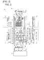
- Figure 2 is a plan view, left/right side views, front view, and back view showing the assembled state in which the three diodes constituting the snubber circuits 32 and the six filter capacitors 82 of the filter circuit 8 have been mounted thereon.
- the components constituting the power converter 3 of the present example overlap one another in plan view, and therefore in the following description, relevant portions are in some instances shown in separate drawings ( Figure 4 , 5 ) to which reference shall be made as well.
- the bidirectional switching elements 31 of the present example are provided, on the upper surface of the module package, with an input terminal of the bidirectional switching element 31, output terminal, and two IGBT midpoint terminals constituting a pair.
- the terminals at the left ends of the three bidirectional switching elements 311, 313, 315 on the left side are input terminals (in Figure 3 these are hidden by the bus bars 333, 334, 335), the terminals at the right ends are output terminals, and the center terminals are midpoint terminals.
- the terminals at the right ends of the three bidirectional switching elements 312, 314, 316 on the right side are input terminals (in Figure 3 these are hidden by the bus bars 333, 334, 335), the terminals at the left ends are output terminals, and the center terminals are midpoint terminals.
- the gate terminals of the bidirectional switching elements 31 are provided to another section of the module package.
- the six bidirectional switching elements 311-316 are fastened to the upper surface of the heat sink 10 by fastening means such as bolts or the like. As shown in the drawings, these six bidirectional switching elements 311-316 are respectively arranged lining up to the left and right of a center line CL, in pairs constituted by the bidirectional switching elements 311 and 312, the bidirectional switching elements 313 and 314, and the bidirectional switching elements 315 and 316.
- the pairs of the two bidirectional switching elements 311 and 312, the bidirectional switching elements 313 and 314, and the bidirectional switching elements 315 and 316 are respectively arranged lining up to the left and right from the center line CL, along the direction of extension of the three terminals (the input terminal, midpoint terminal, and output terminal) of a single bidirectional switching element 31.
- this array is also referred to as "arrangement in rows with respect to the center line CL or to output lines P, N connecting the output terminals.”
- a bidirectional switching element pair refers to a pair of bidirectional switching elements connected to the same phase R, S, or T input line.
- the layout is one in which the output lines P, N (bus bars 331a, 332a) can be led out to minimum length in one direction. Because output of high-frequency AC power over longer wire lengths entails greater susceptibility to the effect of the L component, the effect of the L component can be minimized through the arrangement in the present example.
- the output lines P, N will include the output lines that approximate straight lines, at least up to the transformer 4.
- the terminals at the right ends of the bidirectional switching elements 311, 313, 315 to the left side of the center line CL are all output terminals, while the terminals at the left ends are all input terminals.
- the terminals at the left ends of the bidirectional switching elements 312, 313, 316 to the right side of the center line CL are all output terminals, while the terminals at the right ends are all input terminals.
- the bus bars 333, 334, 335 the input lines R, S, T of the three-phase AC power supply 2 lead towards the center line CL and connect to the input terminals at the left ends of the bidirectional switching elements 311, 313, 315 to the left side of the center line CL, whereas the input lines R, S, T constituted by further extension of these bus bars 333, 334, 335 are connected to the input terminals at the right ends of the bidirectional switching elements 312, 314, 316 to the right side of the center line CL.
- phase R is connected to the input terminals of the bidirectional switching elements 311, 312
- phase S is connected to the input terminals of the bidirectional switching elements 313, 314,
- phase T is connected to the input terminals of the bidirectional switching elements 315, 316, respectively.
- the bus bars 333, 334, 335 constituting the input lines R, S, T lead in one direction from either left or right, and are then extended to the right or left in the other direction, whereby the distance in the left-right direction of the heat sink 10 can be shorter, and the filter capacitors 82L, 82R (discussed later) can be arranged uniformly, contributing to a simpler layout and conserving space.
- the bus bar 333 constituting the input line R is connected between the input terminals of the bidirectional switching elements 311 and 312 constituting a pair arranged to left and right of the center line CL
- the bus bar 334 constituting the input line S is connected between the input terminals of the bidirectional switching elements 313 and 314
- the bus bar 335 constituting the input line T is connected between the input terminals of the bidirectional switching elements 315 and 316.
- the wires corresponding to these bus bars 333, 334, 335 are shown by like symbols in the equivalent circuit of Figure 1 as well.
- the connection structure afforded by these bus bars 333-335 is not essential in terms of the functionality of the power converter 3.
- the pairs constituted by the bidirectional switching elements 311 and 312, the bidirectional switching elements 313 and 314, and the bidirectional switching elements 325 and 316 arranged to left and right from the center line CL are respectively connected by these bus bars 333, 334, 335, whereby the filter capacitors 82L, 82R provided between phases can be mutually shared.
- a filter capacitor 821 is provided between phase R and phase S at the left side in the drawing
- a filter capacitor 824 is provided between phase R and phase S at the right side, the input terminals of the bidirectional switching elements 311, 312 to which phase R is input being connected by the bus bar 333.
- phase R of the three-phase AC power supply 2 is filtered through cooperation by the two filter capacitors 821, 824, whereby a single filter capacitor can be smaller in capacity, as a result of which the filter capacitor can be smaller in size.
- phase S and phase T are the same are true for phase S and phase T as well.
- bus bars 333-335 and the bus bars 331, 332 constituting the output lines P, N intersect in plan view, but as shown in front view in Figures 2 and 5 , the bus bars 331, 332 of the output lines P, N are established at locations higher than the bus bars 333-335 which interconnect the input terminals, thereby providing a constitution that avoids interference resulting from three-dimensional intersection.
- the input lines R, S, T leading from the three-phase AC power supply 2 to the power converter 3 are constituted so as to branch between the filter reactor 81 and the filter capacitors 82L, 82R, but may instead branch to the upstream side from the filter reactor 81, furnishing the filter reactor 81 respectively to the branched input lines R, S, T.
- the single bus bar 331a constituting the output line P of the power converter 3 is connected to the output terminals at the right ends of the bidirectional switching elements 311, 313, 315 to the left side from the center line CL, whereas the single bus bar 332a constituting the output line N of the power converter 3 is connected to the output terminals at the left ends of the bidirectional switching elements 312, 314, 316 to the right side from the center line CL.
- These bus bars 331a, 332a are connected at the distal end side to the transformer 4.
- the following bus bars, including these bus bars 331a, 332a, are constituted by conductors of excellent conductivity, such as copper or the like.
- the pair of bus bars 331a, 332a constituting the output lines P, N of the power converter 3 are relatively wider in shape than bus bars 331b, 332b discussed below, and as shown in plan view and front view in Figure 2 , are arranged lining up upright with respect to a principal surface of the heat sink 10.
- the width dimensions of these bus bars 331a, 332a are selected according to the rated current; wider shape allows for greater current flow, due to the skin effect observed with a high-frequency current.
- the distance between the left-side bidirectional switching elements 311, 313, 315 and the right-side bidirectional switching elements 312, 314, 316 can be shorter, and the power converter 3 can be smaller in the left-right direction.
- each single bus bar 331b, 332b respectively includes multiple (in the present example, two) bus bars arranged stacked at predetermined spacing.
- the current density of high-frequency current would be greater due to the skin effect; however, by virtue of being constituted of a plurality of bus bars, high-frequency current flow comparable to that of the bus bars 331b, 332b can be achieved.
- the bus bars 331b, 332b By arranging the bus bars 331b, 332b to line up in a horizontal direction, the right-end connection terminals to the transformer 4 can be arrayed in the same orientation, as shown in plan view in Figure 2 .
- the filter circuit 8 includes the six filter capacitors 821-826 respectively arranged in sets of three on the input lines, to the left side and the right side of the center line CL as shown in Figures 2 , 4 , and 5 .
- the filter capacitor 821 on the left side is provided between phase R and phase S corresponding to the input terminal of the bidirectional switching element 311.
- the filter capacitor 822 on the left side is provided between phase S and phase T corresponding to the input terminal of the bidirectional switching element 313, and the filter capacitor 823 on the left side is provided between phase T and phase R corresponding to the input terminal of the bidirectional switching element 315.
- the filter capacitor 824 on the right side is provided between phase R and phase S corresponding to the input terminal of the bidirectional switching element 312, the filter capacitor 825 on the right side is provided between phase S and phase T corresponding to the input terminal of the bidirectional switching element 314, and the filter capacitor 826 on the right side is provided between phase T and phase R corresponding to the input terminal of the bidirectional switching element 316.
- the distances over which the respective connecting wires of the filter capacitors 821-826 and the bidirectional switching elements 311-316 are routed can be shorter.
- the filter capacitors 821-826 in sets of three respectively situated at left and right are arranged to the outside, with respect to the center line CL, from the area in which the six bidirectional switching elements 311-316 are provided.
- the elements are fastened to the upper part of the bus bars 333, 334, 335.
- the spacing in the left-right direction between the left and right bidirectional switching elements 311-316 can be shortest, the span of the heat sink 10 in the left-right direction can be set to the shortest span, and as a result the heat sink 10 can be more compact, as compared with the case in which the six filter capacitors are arrayed at the center.
- the bus bar 331a connects the output terminals of the bidirectional switching elements 311, 313, 315, and serves as the output line P leading to the transformer 4 through the bus bar 331b.
- the bus bar 332a connects the output terminals of the bidirectional switching elements 312, 314, 316, and serves as the output line N leading to the transformer 4 through the bus bar 332b.
- the bus bar 333 is a bus bar to which the phase R input line is connected and which connects the input terminals of the bidirectional switching elements 311 and 312, and extends [to areas] to the outside to left and right from both input terminals, in which [areas] the filter capacitors 821, 823, 824, 826 are connected directly.
- the bus bar 334 is a bus bar to which the phase S input line is connected and which connects the input terminals of the bidirectional switching elements 313 and 314, and extends [to areas] to the outside to left and right from both input terminals, in which [areas] the filter capacitors 821, 822, 824, 825 are connected directly.
- the bus bar 335 is a bus bar to which the phase T input line is connected and which connects the input terminals of the bidirectional switching elements 315 and 316, and extends [to areas] to the outside to left and right from both input terminals, in which [areas] the filter capacitors 822, 823, 825, 826 are connected directly. Because the filter capacitors 821-826 directly connect to the bus bars 333-335 in this way, the connection structure is simpler.
- the filter capacitors 82L-82L in sets of three respectively arranged at left and right, are arranged to the outside with respect to the center line CL, and moreover are arranged such that the centers of the filter capacitors 821, 822, 823 are positioned at the apices of a triangle (more preferably an isosceles triangle or an equilateral triangle) one apex of which faces towards an outward direction.
- the wire lengths among the capacitors can be set to the shortest distance, the power converter 3 can be made more compact, and the capacitors can be tuned to one another.
- the filter capacitors 821-826 are arranged on the upper surfaces of the bus bars, in other words, arranging the filter capacitors 821-826 on the opposite side of the bus bars from the bidirectional switching elements 311-316, the degree of freedom in design of the layout of the filter capacitors 821-826 is greater.
- a relatively large electrolytic capacitor is used for the snubber capacitor 327, and the snubber capacitor 327 is shared by the six snubber circuits 321-326 (see Figure 2 ).
- the snubber capacitor 327 and the three diodes are connected by wires.
- the filter capacitors 82L, 82R in sets of three respectively to the left and right, are arranged to the outside, with respect to the center line CL, from the bidirectional switching elements 311, 313, 315 and 312, 314, 316, but could instead be arranged between the bidirectional switching elements 311, 313, 315 and 312, 314, 316 which are arrayed to left and right with respect to the center line CL.
- the bidirectional switching elements 311, 313, 315 are arranged to the left side, and the bidirectional switching elements and 312, 314, 316 are arranged to the right side, with respect to the center line CL.
- the bidirectional switching elements 311, 313, 315 are arranged to the left side, and the bidirectional switching elements and 312, 314, 316 arranged to the right side, with respect to the center line CL, while furnishing the input terminals and the output terminals of the bidirectional switching elements in line-symmetric fashion side with respect to the center line CL.
- the filter capacitors 821-826 are provided between phases, doing so such that each single one corresponds respectively to one of the six bidirectional switching elements 311-316.
- the filter capacitors 821-826 could instead be provided between phases, doing so in such a way that several correspond respectively to one of the six bidirectional switching elements 311-316.
- the filter capacitors may be arranged at the center of the power converter 3, or outside the power converter 3. When arranged at the center of the power converter 3, empty space can be utilized, whereby the size of the power converter 3 can be minimized to the greatest possible extent.
- the aforementioned bidirectional switching elements 311, 313, 315 correspond to the first switching means according to the present invention
- the aforementioned bidirectional switching elements 312, 314, 316 correspond to the second switching means according to the present invention
- the aforementioned power converter 3 corresponds to the conversion circuit according to the present invention
- the aforementioned bus bars 331a, 332a correspond to the first output lines according to the present invention
- the aforementioned bus bars 331b, 332b correspond to the second output lines according to the present invention.
Landscapes
- Engineering & Computer Science (AREA)
- Power Engineering (AREA)
- Microelectronics & Electronic Packaging (AREA)
- Ac-Ac Conversion (AREA)
- Inverter Devices (AREA)
Abstract
Description
- The present invention relates to a power converter for direct conversion of AC power to a desired AC power frequency.
- A matrix converter is one known power converter in which the parts constituting the device are few in number, making possible a smaller device; and which is able to convert AC power directly and efficiently into AC power (Patent Document 1)
- Patent Document 1: Japanese Laid-Open Patent Application
2006-333590 - However, a problem with the aforedescribed matrix converter of the prior art is that multiple IGBT are arranged in series, and the input lines are respectively connected to each of the IGBT, thereby making it difficult to arrange the filter capacitors at uniform distance.
- An object of the present invention is to provide a power converter in which the filter capacitors can be laid out at uniform distance.
- The present invention solves the above-mentioned problem through an arrangement in which the input terminals of multiple pairs of switching means are lined up, and the input lines are led out from one of the switching means and extended to other switching means.
- According to the present invention, multi-phase input lines are lined up along multiple pairs of switching means, whereby the capacitors connected between each of the phases can be arranged at uniform distance.
-
- [
Figure 1 ]
An electrical circuit diagram showing a power conversion system to which an embodiment of the present invention is applied. - [
Figure 2 ]
A plan view, left/right side views, front view, and back view showing the power converter according to an embodiment of the present invention. - [
Figure 3 ]
A plan view of the layout of IGBT, filter capacitors, and bus bars in the power converter ofFigure 2 . - [
Figure 4 ]
A plan view, side view, front view, and back view showing a portion of the power converter ofFigure 2 . - [
Figure 5 ]
A plan view and front view showing in simplified form a portion of the power converter ofFigure 2 . - An overview of a power conversion system to which an embodiment of the present invention is applied shall be described first, making reference to
Figure 1 . The power conversion system 1 of the present example is a system in which three-phase AC power supplied by a three-phaseAC power supply 2 is directly converted to single-phase AC power by apower converter 3 according to an embodiment of the present invention, which power is then stepped up or stepped down, as appropriate, by atransformer 4, and converted to DC voltage by arectifier 5, for use in charging a secondary cell 6. 7 denotes a smoothing circuit. - In the power conversion system 1 of the present example, the phases (shown as phase R, phase S, and phase T) of the output lines which supply three-phase AC power from the three-phase
AC power supply 2 are provided with afilter circuit 8 for attenuation of harmonics, as a countermeasure against noise. Thefilter circuit 8 of the present example is provided with threefilter reactors 81 connected to the phases R, S, and T, and with sixfilter capacitors filter capacitors Figures 2 and4 ) shall be discussed later. - In the power conversion system 1 of the present example, three-phase AC power is supplied to the
power converter 3 through thefilter circuit 8, and converted to single-phase AC power. Thepower converter 3 of the present example is provided with six bidirectional switching elements 31 (311-316) arrayed in a matrix, in corresponding fashion to phase R, phase S, and phase T. In the following description, symbol 31 shall be employed when referring generically to any one bidirectional switching element, whereas [symbols] 311-316 shall be employed when referring to specific elements among the six bidirectional switching elements as shown inFigure 1 . - Each of the bidirectional switching elements 31 in the present example is respectively constituted by an IGBT module in which an IGBT (a type of semiconductor switching element) is combined with a freewheeling diode in an anti-parallel connection. The constitution of a single bidirectional switching element is not limited to that illustrated here, and a different constitution, for example, one involving an anti-parallel connection of two reverse blocking IGBT elements, would also be acceptable.
- In order to protect the bidirectional switching elements 31 from surge voltage generated in association with ON/OFF operation of the bidirectional switching elements 31, the bidirectional switching elements 31 are respectively provided with snubber circuits 32 (321-326) which are a combination of three diodes and one snubber capacitor 327 (see the circuit diagram at lower right in the drawing) at the input side and the output side of the bidirectional switching element 31. In the following description, symbol 32 shall be employed when referring generically to any single snubber circuit, whereas [symbols] 321-326 shall be employed when referring to specific snubber circuits among the six snubber circuits as shown in
Figure 1 . - The power conversion system 1 of the present example is provided with a matrix converter control circuit 9 for respective ON/OFF control of the bidirectional switching elements 31 of the
power converter 3. The matrix converter control circuit 9 inputs the voltage value supplied by the three-phaseAC power supply 2, the currently output DC current value, and a target current command value, and on the basis thereof, controls the respective gate signals of the bidirectional switching elements 31, and adjusts the single-phase AC power output to thetransformer 4, to thereby obtain DC power that matches the target. - The voltage of the single-phase AC power converted by the
power converter 3 is stepped up or stepped down to a predetermined voltage by thetransformer 4. Therectifier 5 is provided with four rectifier diodes 51-54, and converts voltage-regulated single-phase AC power to DC power. Thesmoothing circuit 7 is provided with acoil 71 and acapacitor 72, and smooths pulsating current included in rectified DC current, to produce a condition that more closely approximates DC. - In the power conversion system 1 of the present example constituted in the above manner, three-phase AC power supplied by the three-phase
AC power supply 2 is directly converted to single-phase AC power by thepower converter 3, and after regulation to appropriate voltage, is converted to DC power. The secondary cell 6 is charged thereby. The power conversion system 1 discussed above is merely one example of application of thepower converter 3 according to the present invention, and the present invention is not limited to application in the power conversion system in question. Specifically, application in other power conversion systems is possible as well, provided that at least the power being converted and/or the converted power is multi-phase AC power. - Next, the constitution of arrangement of the components that constitute the
power converter 3 shall be described, making reference toFigures 2 to 5 . Components assigned the same symbols as inFigure 1 indicate those having mutually corresponding relationships. InFigures 2 and3 , therectifier 5 and thesmoothing circuit 7 are shown besides thepower converter 3 of the present example, but thetransformer 4 ofFigure 1 lies outside of the drawing. -
Figure 3 is a plan view showing a mid-assembly state in which the six bidirectional switching elements 31 (any one of which is also referred to as an IGBT module) have been mounted on the upper surface of aheat sink 10, and bus bars for connecting the terminals of the bidirectional switching elements 31 have been mounted thereon.Figure 2 is a plan view, left/right side views, front view, and back view showing the assembled state in which the three diodes constituting the snubber circuits 32 and the six filter capacitors 82 of thefilter circuit 8 have been mounted thereon. The components constituting thepower converter 3 of the present example overlap one another in plan view, and therefore in the following description, relevant portions are in some instances shown in separate drawings (Figure 4 ,5 ) to which reference shall be made as well. - As shown in
Figures 3 and5 , the bidirectional switching elements 31 of the present example are provided, on the upper surface of the module package, with an input terminal of the bidirectional switching element 31, output terminal, and two IGBT midpoint terminals constituting a pair. Of the six bidirectional switching elements 311-316 shown inFigures 3 and5 , the terminals at the left ends of the threebidirectional switching elements Figure 3 these are hidden by thebus bars Figures 3 and5 , the terminals at the right ends of the threebidirectional switching elements Figure 3 these are hidden by thebus bars - As shown in
Figures 2 ,3 , and5 , the six bidirectional switching elements 311-316 are fastened to the upper surface of theheat sink 10 by fastening means such as bolts or the like. As shown in the drawings, these six bidirectional switching elements 311-316 are respectively arranged lining up to the left and right of a center line CL, in pairs constituted by thebidirectional switching elements bidirectional switching elements bidirectional switching elements bidirectional switching elements bidirectional switching elements bidirectional switching elements - By arranging the pairs constituted by the
bidirectional switching elements bidirectional switching elements bidirectional switching elements bus bars transformer 4. - As mentioned above, the terminals at the right ends of the
bidirectional switching elements bidirectional switching elements - The bus bars 333, 334, 335 the input lines R, S, T of the three-phase
AC power supply 2 lead towards the center line CL and connect to the input terminals at the left ends of thebidirectional switching elements bus bars bidirectional switching elements bidirectional switching elements bidirectional switching elements bidirectional switching elements heat sink 10 can be shorter, and thefilter capacitors - The
bus bar 333 constituting the input line R is connected between the input terminals of thebidirectional switching elements bus bar 334 constituting the input line S is connected between the input terminals of thebidirectional switching elements bus bar 335 constituting the input line T is connected between the input terminals of thebidirectional switching elements bus bars Figure 1 as well. The connection structure afforded by these bus bars 333-335 is not essential in terms of the functionality of thepower converter 3. - The pairs constituted by the
bidirectional switching elements bidirectional switching elements bidirectional switching elements bus bars filter capacitors filter capacitor 821 is provided between phase R and phase S at the left side in the drawing, and afilter capacitor 824 is provided between phase R and phase S at the right side, the input terminals of thebidirectional switching elements bus bar 333. Consequently, noise from phase R of the three-phaseAC power supply 2 is filtered through cooperation by the twofilter capacitors - These bus bars 333-335 and the bus bars 331, 332 constituting the output lines P, N intersect in plan view, but as shown in front view in
Figures 2 and5 , the bus bars 331, 332 of the output lines P, N are established at locations higher than the bus bars 333-335 which interconnect the input terminals, thereby providing a constitution that avoids interference resulting from three-dimensional intersection. - In
Figure 1 , the input lines R, S, T leading from the three-phaseAC power supply 2 to thepower converter 3 are constituted so as to branch between thefilter reactor 81 and thefilter capacitors filter reactor 81, furnishing thefilter reactor 81 respectively to the branched input lines R, S, T. - The
single bus bar 331a constituting the output line P of thepower converter 3 is connected to the output terminals at the right ends of thebidirectional switching elements single bus bar 332a constituting the output line N of thepower converter 3 is connected to the output terminals at the left ends of thebidirectional switching elements bus bars transformer 4. The following bus bars, including thesebus bars - The pair of
bus bars power converter 3 are relatively wider in shape thanbus bars Figure 2 , are arranged lining up upright with respect to a principal surface of theheat sink 10. The width dimensions of thesebus bars bidirectional switching elements bidirectional switching elements power converter 3 can be smaller in the left-right direction. - In contrast to this, the pair of
bus bars power converter 3 are connected and fastened to the distal ends of thebus bars heat sink 10 as shown in plan view and front view inFigure 2 . While thesebus bars bus bars Figure 2 , eachsingle bus bar transformer 4 can be arrayed in the same orientation, as shown in plan view inFigure 2 . - In the present example, the
filter circuit 8 includes the six filter capacitors 821-826 respectively arranged in sets of three on the input lines, to the left side and the right side of the center line CL as shown inFigures 2 ,4 , and5 . Thefilter capacitor 821 on the left side is provided between phase R and phase S corresponding to the input terminal of thebidirectional switching element 311. Likewise, thefilter capacitor 822 on the left side is provided between phase S and phase T corresponding to the input terminal of thebidirectional switching element 313, and thefilter capacitor 823 on the left side is provided between phase T and phase R corresponding to the input terminal of thebidirectional switching element 315. Thefilter capacitor 824 on the right side is provided between phase R and phase S corresponding to the input terminal of thebidirectional switching element 312, thefilter capacitor 825 on the right side is provided between phase S and phase T corresponding to the input terminal of thebidirectional switching element 314, and thefilter capacitor 826 on the right side is provided between phase T and phase R corresponding to the input terminal of thebidirectional switching element 316. - By arranging the six filter capacitors 821-826 in sets of three to the left and right of the center line CL in respectively corresponding fashion to the six bidirectional switching elements 311-316 which have been arranged in sets of three each to the left and right of the center line CL in this manner, the distances over which the respective connecting wires of the filter capacitors 821-826 and the bidirectional switching elements 311-316 are routed can be shorter.
- In the present example, the filter capacitors 821-826 in sets of three respectively situated at left and right are arranged to the outside, with respect to the center line CL, from the area in which the six bidirectional switching elements 311-316 are provided. In specific terms, as shown in
Figures 2 ,4 , and5 , the elements are fastened to the upper part of the bus bars 333, 334, 335. By arranging the filter capacitors 821-826 further to the outside from the bidirectional switching elements 311-316, the spacing in the left-right direction between the left and right bidirectional switching elements 311-316 can be shortest, the span of theheat sink 10 in the left-right direction can be set to the shortest span, and as a result theheat sink 10 can be more compact, as compared with the case in which the six filter capacitors are arrayed at the center. - Next, the mounted condition of the filter capacitors 821-826 provided in sets of three respectively to the left and right of the center line CL will be described on the basis of the plan views and side views of the actual device shown in
Figures 2 to 4 . - Before doing so, the connection configuration of the bus bars shall be described again. As shown in
Figure 3 , thebus bar 331a connects the output terminals of thebidirectional switching elements transformer 4 through thebus bar 331b. Thebus bar 332a connects the output terminals of thebidirectional switching elements transformer 4 through thebus bar 332b. - The
bus bar 333 is a bus bar to which the phase R input line is connected and which connects the input terminals of thebidirectional switching elements filter capacitors bus bar 334 is a bus bar to which the phase S input line is connected and which connects the input terminals of thebidirectional switching elements filter capacitors bus bar 335 is a bus bar to which the phase T input line is connected and which connects the input terminals of thebidirectional switching elements filter capacitors - As shown in
Figures 2 ,4 , and5 , thefilter capacitors 82L-82L, in sets of three respectively arranged at left and right, are arranged to the outside with respect to the center line CL, and moreover are arranged such that the centers of thefilter capacitors filter capacitors power converter 3 can be made more compact, and the capacitors can be tuned to one another. Moreover, by arranging one apex to face towards an outward direction, the balance among the wires connecting the capacitors can be improved, and the distances to the bus bars 333, 334, 335, can be shorter, as compared to an array in which one apex faces towards an inward direction. Furthermore, by arranging the filter capacitors 821-826 on the upper surfaces of the bus bars, in other words, arranging the filter capacitors 821-826 on the opposite side of the bus bars from the bidirectional switching elements 311-316, the degree of freedom in design of the layout of the filter capacitors 821-826 is greater. - Next, an example of mounting the three diodes and the one
snubber capacitor 327 constituting the snubber circuit 32 shown inFigure 1 will be described. As shown inFigure 1 , in thesnubber circuit 321 of thebidirectional switching element 311 for example, one terminal is connected to the input terminal of thebidirectional switching element 311, another terminal is connected to the midpoint terminal of the bidirectional switching element, and yet another terminal is connected to the output terminal of thebidirectional switching element 311, respectively. Therefore, as shown inFigure 2 , the three diodes are respectively fastened and connected to brackets 351-356 comprising conductors which are connected to the midpoint terminals of the bidirectional switching elements 31L, 31R. - In the present example, a relatively large electrolytic capacitor is used for the
snubber capacitor 327, and thesnubber capacitor 327 is shared by the six snubber circuits 321-326 (seeFigure 2 ). Thesnubber capacitor 327 and the three diodes are connected by wires. - The embodiment shown above has the following effects.
- 1) According to the present example, the six filter capacitors 821-826, in sets of three to the left and right of the center line CL, are arranged in respectively corresponding fashion to the six bidirectional switching elements 311-316 which have been arranged in sets of three to the left and right of the center line CL, whereby the distances over which the respective connecting wires of the filter capacitors 821-826 and the bidirectional switching elements 311-316 are routed can be shorter.
- 2) In the present example, the pairs of the
bidirectional switching elements bidirectional switching elements bidirectional switching elements bus bars - 3) In the present example, the pair of
bus bars heat sink 10. The wider shape allows for greater current flow, due to the skin effect observed with a high-frequency current. Moreover, by adopting a wider shape and an upright arrangement, the distance between the left-sidebidirectional switching elements bidirectional switching elements power converter 3 can be smaller in the left-right direction. - 4) In the present example, the bus bars 331b, 332b constituting the output lines P, N are narrower in width relative to the
bus bars heat sink 10. Due to the narrower width of the bus bars 331b, 332b relative to thebus bars transformer 4 can be arrayed in the same orientation. Moreover, because a single bus bar includes multiple bus bars stacked at predetermined spacing, high-frequency current flow comparable to that through thebus bars - 5) In the present example, the filter capacitors 821-826 in sets of three respectively situated at left and right are arranged to the outside, with respect to the center line CL, from the area in which the six bidirectional switching elements 311-316 are provided, whereby the spacing in the left-right direction between the left and right bidirectional switching elements 31L, 31R can be shortest. Consequently, the span of the
heat sink 10 in the left-right direction can be set to the shortest span, and as a result theheat sink 10 can be more compact. - 6) In the present example, the bus bars 333, 334 constituting the input lines lead in one direction from either left or right, and extend to right or left in the other direction, thereby respectively connecting the input terminals of the pairs of the
bidirectional switching elements bidirectional switching elements bidirectional switching elements heat sink 10 in the left-right direction can be shorter, and thefilter capacitors filter capacitors - 7) In the present example, the filter capacitors 821-826 are arranged on the upper surfaces of the bus bars 333, 334, 335, in other words, the filter capacitors 821-826 are arranged on the opposite side of the bus bars from the bidirectional switching elements 311-316, thereby affording a greater degree of freedom in design of the layout of the filter capacitors 821-826.
- 8) In the present example, the three
filter capacitors power converter 3 can be made more compact, and the capacitors can be tuned to one another. - 9) In the present example, the three filter capacitors arranged a triangle are arranged such that one apex faces towards an outward direction, whereby the balance among the wires connecting the capacitors can be improved, and the distances to the bus bars 333, 334, 335, can be shorter, as compared to an array in which one apex faces towards an inward direction.
- The present invention can be modified, as appropriate, to embodiments other than the preceding. While modifications of the present invention are described below, the present invention should not be construed as being limited to the preceding embodiment or to the embodiments hereinbelow.
- In the preceding embodiment, the
filter capacitors bidirectional switching elements bidirectional switching elements - In the preceding embodiment, of the six bidirectional switching elements 311-316, the
bidirectional switching elements bidirectional switching elements - In the preceding embodiment, of the six bidirectional switching elements 311-316, the
bidirectional switching elements bidirectional switching elements bidirectional switching elements - In the preceding embodiment, the filter capacitors 821-826 are provided between phases, doing so such that each single one corresponds respectively to one of the six bidirectional switching elements 311-316. However, the filter capacitors 821-826 could instead be provided between phases, doing so in such a way that several correspond respectively to one of the six bidirectional switching elements 311-316. In this case, the filter capacitors may be arranged at the center of the
power converter 3, or outside thepower converter 3. When arranged at the center of thepower converter 3, empty space can be utilized, whereby the size of thepower converter 3 can be minimized to the greatest possible extent. - The aforementioned
bidirectional switching elements bidirectional switching elements aforementioned power converter 3 corresponds to the conversion circuit according to the present invention; theaforementioned bus bars -
- 1:
- power conversion system
- 2:
- three-phase AC power supply
- 3:
- power converter
31, 311-316: bidirectional switching elements
32, 321-326: snubber circuits
327: snubber capacitor
341-348: bus bars
351-356: brackets - 4:
- transformer
- 5:
- rectifier
- 6:
- secondary cell
- 7:
- smoothing circuit
- 8:
- filter circuit
81: filter reactor
82L, 82R, 821-826, 831-836: filter capacitors - 9:
- matrix converter control circuit
- 10:
- heat sink
Claims (7)
- A power converter for direct conversion of multi-phase AC power to AC power, the power converter comprising:a conversion circuit having a plurality of first switching means connected to the phases of the multi-phase AC power, and capable of bidirectional switching of energizing current, and a plurality of second switching means connected to the phases of the multi-phase AC power, and capable of bidirectional switching of energizing current;input lines connected to the conversion circuit; anda plurality of capacitors connected to the conversion circuit;in the plurality of first switching means and the plurality of second switching means,paired input terminals being arranged lining up in a row; andthe input lines leading in one direction in which the paired input terminals line up, and extending from one input terminal to the other input terminal.
- The power converter according to claim 1, wherein the plurality of capacitors are arranged to the outside with respect to the first switching means and the second switching means.
- The power converter according to claim 2, wherein a connection is established between the capacitors connected to the first switching means and the capacitors connected to the second switching means.
- The power converter according to any of claims 1 to 3, further comprising output lines connected to the conversion circuit;
the output terminals of the plurality of first switching means and the plurality of second switching means being respectively lined up in a row; and
the output lines
including a pair of first output lines that are connected to the output terminals, led out in one direction, and provided with bus bars of wide shape arranged lining up in an upright direction. - The power converter according to claim 4, wherein the output lines include a pair of second output lines that are connected to distal ends of the pair of first output lines, fashioned narrower in width than the first output lines, and arranged in a horizontal direction,
a plurality of output lines being stacked at predetermined spacing in each of the second output lines. - The power converter according to claim 4 or 5, wherein the output lines are arranged to the upper side of the input lines in a vertical direction.
- The power converter according to any of claims 4 to 6, wherein the output lines are connected to output terminals provided to the inside from the input terminals.
Applications Claiming Priority (2)
| Application Number | Priority Date | Filing Date | Title |
|---|---|---|---|
| JP2011223289 | 2011-10-07 | ||
| PCT/JP2012/075097 WO2013051476A1 (en) | 2011-10-07 | 2012-09-28 | Power converter |
Publications (3)
| Publication Number | Publication Date |
|---|---|
| EP2765700A1 true EP2765700A1 (en) | 2014-08-13 |
| EP2765700A4 EP2765700A4 (en) | 2016-04-13 |
| EP2765700B1 EP2765700B1 (en) | 2017-04-26 |
Family
ID=48043636
Family Applications (1)
| Application Number | Title | Priority Date | Filing Date |
|---|---|---|---|
| EP12838013.6A Not-in-force EP2765700B1 (en) | 2011-10-07 | 2012-09-28 | Power converter |
Country Status (5)
| Country | Link |
|---|---|
| US (1) | US9369055B2 (en) |
| EP (1) | EP2765700B1 (en) |
| JP (1) | JP5420122B2 (en) |
| CN (1) | CN103858329B (en) |
| WO (1) | WO2013051476A1 (en) |
Families Citing this family (9)
| Publication number | Priority date | Publication date | Assignee | Title |
|---|---|---|---|---|
| JP5437312B2 (en) | 2011-05-31 | 2014-03-12 | 日産自動車株式会社 | Power converter |
| JP5377575B2 (en) * | 2011-05-31 | 2013-12-25 | 日産自動車株式会社 | Power converter |
| JP5377574B2 (en) | 2011-05-31 | 2013-12-25 | 日産自動車株式会社 | Power converter |
| CN103875169B (en) * | 2011-10-07 | 2017-03-01 | 日产自动车株式会社 | power conversion device |
| US9973107B2 (en) * | 2014-08-13 | 2018-05-15 | Inesc Tec—Instituto de Engenharia de Sistemas | AC/DC converter with three to single phase matrix converter, full-bridge AC/DC converter and HF transformer |
| US11251618B2 (en) * | 2015-01-21 | 2022-02-15 | Enphase Energy, Inc. | Apparatus and method for reactive power control |
| JP6477893B2 (en) * | 2015-08-28 | 2019-03-06 | 株式会社村田製作所 | DC-DC converter |
| JP6504622B2 (en) | 2017-06-14 | 2019-04-24 | 三菱電機株式会社 | Capacitor substrate unit for open / close module, open / close module, and motor drive device |
| WO2025142105A1 (en) * | 2023-12-28 | 2025-07-03 | 株式会社村田製作所 | Power conversion circuit |
Family Cites Families (21)
| Publication number | Priority date | Publication date | Assignee | Title |
|---|---|---|---|---|
| JPH0628292B2 (en) * | 1988-11-11 | 1994-04-13 | 富士電機株式会社 | Reverse blocking transistor module |
| JPH06261556A (en) * | 1993-03-04 | 1994-09-16 | Toshiba Corp | Semiconductor switch apparatus |
| JP2001045772A (en) * | 1999-08-03 | 2001-02-16 | Yaskawa Electric Corp | 3-level inverter or PWM cycloconverter |
| JP2004236374A (en) * | 2003-01-28 | 2004-08-19 | Fuji Electric Holdings Co Ltd | Configuration method of AC-AC direct conversion type power converter |
| JP4337443B2 (en) * | 2003-08-12 | 2009-09-30 | 株式会社日立製作所 | Matrix converter system |
| JP4385672B2 (en) * | 2003-08-12 | 2009-12-16 | 株式会社日立製作所 | Power converter using matrix converter |
| JP4765017B2 (en) | 2005-05-25 | 2011-09-07 | 富士電機株式会社 | AC-AC power converter |
| DE112007000366T5 (en) * | 2006-02-17 | 2009-01-02 | Kabushiki Kaisha Yaskawa Denki, Kitakyushu | Power conversion device with busbar |
| JP4720756B2 (en) * | 2007-02-22 | 2011-07-13 | トヨタ自動車株式会社 | Semiconductor power conversion device and manufacturing method thereof |
| US20090052134A1 (en) * | 2007-08-22 | 2009-02-26 | Casteel Jordan B | Liquid-cooled grounded heatsink for diode rectifier system |
| EP2099119B1 (en) * | 2008-03-04 | 2014-11-19 | Kabushiki Kaisha Toyota Jidoshokki | Power converter apparatus |
| JP5273027B2 (en) | 2009-12-02 | 2013-08-28 | 株式会社デンソー | Power converter |
| JP2012054449A (en) * | 2010-09-02 | 2012-03-15 | Aisin Aw Co Ltd | Electric connection device |
| EP2512023A3 (en) * | 2011-04-14 | 2017-06-28 | General Electric Technology GmbH | Power converter arrangement and method for operating a power converter arrangement |
| JP5437312B2 (en) * | 2011-05-31 | 2014-03-12 | 日産自動車株式会社 | Power converter |
| JP5377574B2 (en) * | 2011-05-31 | 2013-12-25 | 日産自動車株式会社 | Power converter |
| JP5437313B2 (en) * | 2011-05-31 | 2014-03-12 | 日産自動車株式会社 | Power converter |
| JP5437314B2 (en) * | 2011-05-31 | 2014-03-12 | 日産自動車株式会社 | Power converter |
| JP5377575B2 (en) * | 2011-05-31 | 2013-12-25 | 日産自動車株式会社 | Power converter |
| JP5377573B2 (en) * | 2011-05-31 | 2013-12-25 | 日産自動車株式会社 | Power converter |
| CN103875169B (en) * | 2011-10-07 | 2017-03-01 | 日产自动车株式会社 | power conversion device |
-
2012
- 2012-09-28 US US14/349,686 patent/US9369055B2/en not_active Expired - Fee Related
- 2012-09-28 CN CN201280049145.XA patent/CN103858329B/en not_active Expired - Fee Related
- 2012-09-28 JP JP2013537349A patent/JP5420122B2/en not_active Expired - Fee Related
- 2012-09-28 WO PCT/JP2012/075097 patent/WO2013051476A1/en not_active Ceased
- 2012-09-28 EP EP12838013.6A patent/EP2765700B1/en not_active Not-in-force
Also Published As
| Publication number | Publication date |
|---|---|
| CN103858329B (en) | 2017-03-29 |
| US20140247635A1 (en) | 2014-09-04 |
| EP2765700B1 (en) | 2017-04-26 |
| WO2013051476A1 (en) | 2013-04-11 |
| EP2765700A4 (en) | 2016-04-13 |
| JPWO2013051476A1 (en) | 2015-03-30 |
| JP5420122B2 (en) | 2014-02-19 |
| US9369055B2 (en) | 2016-06-14 |
| CN103858329A (en) | 2014-06-11 |
Similar Documents
| Publication | Publication Date | Title |
|---|---|---|
| EP2765699B1 (en) | Power converter | |
| EP2765700B1 (en) | Power converter | |
| US8958210B2 (en) | Modular converter cabinet system | |
| JP5377575B2 (en) | Power converter | |
| JP5437314B2 (en) | Power converter | |
| JP5437312B2 (en) | Power converter | |
| JP5437313B2 (en) | Power converter | |
| JP5377573B2 (en) | Power converter | |
| JP5377574B2 (en) | Power converter |
Legal Events
| Date | Code | Title | Description |
|---|---|---|---|
| PUAI | Public reference made under article 153(3) epc to a published international application that has entered the european phase |
Free format text: ORIGINAL CODE: 0009012 |
|
| 17P | Request for examination filed |
Effective date: 20140428 |
|
| AK | Designated contracting states |
Kind code of ref document: A1 Designated state(s): AL AT BE BG CH CY CZ DE DK EE ES FI FR GB GR HR HU IE IS IT LI LT LU LV MC MK MT NL NO PL PT RO RS SE SI SK SM TR |
|
| DAX | Request for extension of the european patent (deleted) | ||
| RA4 | Supplementary search report drawn up and despatched (corrected) |
Effective date: 20160315 |
|
| RIC1 | Information provided on ipc code assigned before grant |
Ipc: H02M 5/293 20060101AFI20160309BHEP Ipc: H02M 5/297 20060101ALI20160309BHEP Ipc: H05K 7/14 20060101ALI20160309BHEP |
|
| GRAP | Despatch of communication of intention to grant a patent |
Free format text: ORIGINAL CODE: EPIDOSNIGR1 |
|
| INTG | Intention to grant announced |
Effective date: 20161223 |
|
| GRAS | Grant fee paid |
Free format text: ORIGINAL CODE: EPIDOSNIGR3 |
|
| GRAA | (expected) grant |
Free format text: ORIGINAL CODE: 0009210 |
|
| AK | Designated contracting states |
Kind code of ref document: B1 Designated state(s): AL AT BE BG CH CY CZ DE DK EE ES FI FR GB GR HR HU IE IS IT LI LT LU LV MC MK MT NL NO PL PT RO RS SE SI SK SM TR |
|
| REG | Reference to a national code |
Ref country code: GB Ref legal event code: FG4D |
|
| REG | Reference to a national code |
Ref country code: CH Ref legal event code: EP |
|
| REG | Reference to a national code |
Ref country code: AT Ref legal event code: REF Ref document number: 888663 Country of ref document: AT Kind code of ref document: T Effective date: 20170515 |
|
| REG | Reference to a national code |
Ref country code: IE Ref legal event code: FG4D |
|
| REG | Reference to a national code |
Ref country code: DE Ref legal event code: R096 Ref document number: 602012031733 Country of ref document: DE |
|
| REG | Reference to a national code |
Ref country code: NL Ref legal event code: MP Effective date: 20170426 |
|
| REG | Reference to a national code |
Ref country code: LT Ref legal event code: MG4D |
|
| REG | Reference to a national code |
Ref country code: AT Ref legal event code: MK05 Ref document number: 888663 Country of ref document: AT Kind code of ref document: T Effective date: 20170426 |
|
| REG | Reference to a national code |
Ref country code: FR Ref legal event code: PLFP Year of fee payment: 6 |
|
| PG25 | Lapsed in a contracting state [announced via postgrant information from national office to epo] |
Ref country code: NL Free format text: LAPSE BECAUSE OF FAILURE TO SUBMIT A TRANSLATION OF THE DESCRIPTION OR TO PAY THE FEE WITHIN THE PRESCRIBED TIME-LIMIT Effective date: 20170426 |
|
| PG25 | Lapsed in a contracting state [announced via postgrant information from national office to epo] |
Ref country code: GR Free format text: LAPSE BECAUSE OF FAILURE TO SUBMIT A TRANSLATION OF THE DESCRIPTION OR TO PAY THE FEE WITHIN THE PRESCRIBED TIME-LIMIT Effective date: 20170727 Ref country code: AT Free format text: LAPSE BECAUSE OF FAILURE TO SUBMIT A TRANSLATION OF THE DESCRIPTION OR TO PAY THE FEE WITHIN THE PRESCRIBED TIME-LIMIT Effective date: 20170426 Ref country code: NO Free format text: LAPSE BECAUSE OF FAILURE TO SUBMIT A TRANSLATION OF THE DESCRIPTION OR TO PAY THE FEE WITHIN THE PRESCRIBED TIME-LIMIT Effective date: 20170726 Ref country code: ES Free format text: LAPSE BECAUSE OF FAILURE TO SUBMIT A TRANSLATION OF THE DESCRIPTION OR TO PAY THE FEE WITHIN THE PRESCRIBED TIME-LIMIT Effective date: 20170426 Ref country code: LT Free format text: LAPSE BECAUSE OF FAILURE TO SUBMIT A TRANSLATION OF THE DESCRIPTION OR TO PAY THE FEE WITHIN THE PRESCRIBED TIME-LIMIT Effective date: 20170426 Ref country code: HR Free format text: LAPSE BECAUSE OF FAILURE TO SUBMIT A TRANSLATION OF THE DESCRIPTION OR TO PAY THE FEE WITHIN THE PRESCRIBED TIME-LIMIT Effective date: 20170426 Ref country code: FI Free format text: LAPSE BECAUSE OF FAILURE TO SUBMIT A TRANSLATION OF THE DESCRIPTION OR TO PAY THE FEE WITHIN THE PRESCRIBED TIME-LIMIT Effective date: 20170426 |
|
| PG25 | Lapsed in a contracting state [announced via postgrant information from national office to epo] |
Ref country code: RS Free format text: LAPSE BECAUSE OF FAILURE TO SUBMIT A TRANSLATION OF THE DESCRIPTION OR TO PAY THE FEE WITHIN THE PRESCRIBED TIME-LIMIT Effective date: 20170426 Ref country code: LV Free format text: LAPSE BECAUSE OF FAILURE TO SUBMIT A TRANSLATION OF THE DESCRIPTION OR TO PAY THE FEE WITHIN THE PRESCRIBED TIME-LIMIT Effective date: 20170426 Ref country code: IS Free format text: LAPSE BECAUSE OF FAILURE TO SUBMIT A TRANSLATION OF THE DESCRIPTION OR TO PAY THE FEE WITHIN THE PRESCRIBED TIME-LIMIT Effective date: 20170826 Ref country code: PL Free format text: LAPSE BECAUSE OF FAILURE TO SUBMIT A TRANSLATION OF THE DESCRIPTION OR TO PAY THE FEE WITHIN THE PRESCRIBED TIME-LIMIT Effective date: 20170426 Ref country code: SE Free format text: LAPSE BECAUSE OF FAILURE TO SUBMIT A TRANSLATION OF THE DESCRIPTION OR TO PAY THE FEE WITHIN THE PRESCRIBED TIME-LIMIT Effective date: 20170426 Ref country code: BG Free format text: LAPSE BECAUSE OF FAILURE TO SUBMIT A TRANSLATION OF THE DESCRIPTION OR TO PAY THE FEE WITHIN THE PRESCRIBED TIME-LIMIT Effective date: 20170726 |
|
| REG | Reference to a national code |
Ref country code: DE Ref legal event code: R097 Ref document number: 602012031733 Country of ref document: DE |
|
| PG25 | Lapsed in a contracting state [announced via postgrant information from national office to epo] |
Ref country code: DK Free format text: LAPSE BECAUSE OF FAILURE TO SUBMIT A TRANSLATION OF THE DESCRIPTION OR TO PAY THE FEE WITHIN THE PRESCRIBED TIME-LIMIT Effective date: 20170426 Ref country code: EE Free format text: LAPSE BECAUSE OF FAILURE TO SUBMIT A TRANSLATION OF THE DESCRIPTION OR TO PAY THE FEE WITHIN THE PRESCRIBED TIME-LIMIT Effective date: 20170426 Ref country code: CZ Free format text: LAPSE BECAUSE OF FAILURE TO SUBMIT A TRANSLATION OF THE DESCRIPTION OR TO PAY THE FEE WITHIN THE PRESCRIBED TIME-LIMIT Effective date: 20170426 Ref country code: RO Free format text: LAPSE BECAUSE OF FAILURE TO SUBMIT A TRANSLATION OF THE DESCRIPTION OR TO PAY THE FEE WITHIN THE PRESCRIBED TIME-LIMIT Effective date: 20170426 Ref country code: SK Free format text: LAPSE BECAUSE OF FAILURE TO SUBMIT A TRANSLATION OF THE DESCRIPTION OR TO PAY THE FEE WITHIN THE PRESCRIBED TIME-LIMIT Effective date: 20170426 |
|
| PG25 | Lapsed in a contracting state [announced via postgrant information from national office to epo] |
Ref country code: IT Free format text: LAPSE BECAUSE OF FAILURE TO SUBMIT A TRANSLATION OF THE DESCRIPTION OR TO PAY THE FEE WITHIN THE PRESCRIBED TIME-LIMIT Effective date: 20170426 Ref country code: SM Free format text: LAPSE BECAUSE OF FAILURE TO SUBMIT A TRANSLATION OF THE DESCRIPTION OR TO PAY THE FEE WITHIN THE PRESCRIBED TIME-LIMIT Effective date: 20170426 |
|
| PLBE | No opposition filed within time limit |
Free format text: ORIGINAL CODE: 0009261 |
|
| STAA | Information on the status of an ep patent application or granted ep patent |
Free format text: STATUS: NO OPPOSITION FILED WITHIN TIME LIMIT |
|
| 26N | No opposition filed |
Effective date: 20180129 |
|
| REG | Reference to a national code |
Ref country code: CH Ref legal event code: PL |
|
| PG25 | Lapsed in a contracting state [announced via postgrant information from national office to epo] |
Ref country code: MC Free format text: LAPSE BECAUSE OF FAILURE TO SUBMIT A TRANSLATION OF THE DESCRIPTION OR TO PAY THE FEE WITHIN THE PRESCRIBED TIME-LIMIT Effective date: 20170426 Ref country code: SI Free format text: LAPSE BECAUSE OF FAILURE TO SUBMIT A TRANSLATION OF THE DESCRIPTION OR TO PAY THE FEE WITHIN THE PRESCRIBED TIME-LIMIT Effective date: 20170426 |
|
| REG | Reference to a national code |
Ref country code: IE Ref legal event code: MM4A |
|
| REG | Reference to a national code |
Ref country code: BE Ref legal event code: MM Effective date: 20170930 |
|
| PG25 | Lapsed in a contracting state [announced via postgrant information from national office to epo] |
Ref country code: LU Free format text: LAPSE BECAUSE OF NON-PAYMENT OF DUE FEES Effective date: 20170928 |
|
| PG25 | Lapsed in a contracting state [announced via postgrant information from national office to epo] |
Ref country code: CH Free format text: LAPSE BECAUSE OF NON-PAYMENT OF DUE FEES Effective date: 20170930 Ref country code: LI Free format text: LAPSE BECAUSE OF NON-PAYMENT OF DUE FEES Effective date: 20170930 Ref country code: IE Free format text: LAPSE BECAUSE OF NON-PAYMENT OF DUE FEES Effective date: 20170928 |
|
| REG | Reference to a national code |
Ref country code: FR Ref legal event code: PLFP Year of fee payment: 7 |
|
| PG25 | Lapsed in a contracting state [announced via postgrant information from national office to epo] |
Ref country code: BE Free format text: LAPSE BECAUSE OF NON-PAYMENT OF DUE FEES Effective date: 20170930 |
|
| PG25 | Lapsed in a contracting state [announced via postgrant information from national office to epo] |
Ref country code: MT Free format text: LAPSE BECAUSE OF NON-PAYMENT OF DUE FEES Effective date: 20170928 |
|
| PG25 | Lapsed in a contracting state [announced via postgrant information from national office to epo] |
Ref country code: HU Free format text: LAPSE BECAUSE OF FAILURE TO SUBMIT A TRANSLATION OF THE DESCRIPTION OR TO PAY THE FEE WITHIN THE PRESCRIBED TIME-LIMIT; INVALID AB INITIO Effective date: 20120928 |
|
| PG25 | Lapsed in a contracting state [announced via postgrant information from national office to epo] |
Ref country code: CY Free format text: LAPSE BECAUSE OF FAILURE TO SUBMIT A TRANSLATION OF THE DESCRIPTION OR TO PAY THE FEE WITHIN THE PRESCRIBED TIME-LIMIT Effective date: 20170426 |
|
| PGFP | Annual fee paid to national office [announced via postgrant information from national office to epo] |
Ref country code: FR Payment date: 20190815 Year of fee payment: 8 Ref country code: DE Payment date: 20190917 Year of fee payment: 8 |
|
| PG25 | Lapsed in a contracting state [announced via postgrant information from national office to epo] |
Ref country code: MK Free format text: LAPSE BECAUSE OF FAILURE TO SUBMIT A TRANSLATION OF THE DESCRIPTION OR TO PAY THE FEE WITHIN THE PRESCRIBED TIME-LIMIT Effective date: 20170426 |
|
| PGFP | Annual fee paid to national office [announced via postgrant information from national office to epo] |
Ref country code: GB Payment date: 20190926 Year of fee payment: 8 |
|
| PG25 | Lapsed in a contracting state [announced via postgrant information from national office to epo] |
Ref country code: TR Free format text: LAPSE BECAUSE OF FAILURE TO SUBMIT A TRANSLATION OF THE DESCRIPTION OR TO PAY THE FEE WITHIN THE PRESCRIBED TIME-LIMIT Effective date: 20170426 |
|
| PG25 | Lapsed in a contracting state [announced via postgrant information from national office to epo] |
Ref country code: PT Free format text: LAPSE BECAUSE OF FAILURE TO SUBMIT A TRANSLATION OF THE DESCRIPTION OR TO PAY THE FEE WITHIN THE PRESCRIBED TIME-LIMIT Effective date: 20170426 |
|
| PG25 | Lapsed in a contracting state [announced via postgrant information from national office to epo] |
Ref country code: AL Free format text: LAPSE BECAUSE OF FAILURE TO SUBMIT A TRANSLATION OF THE DESCRIPTION OR TO PAY THE FEE WITHIN THE PRESCRIBED TIME-LIMIT Effective date: 20170426 |
|
| REG | Reference to a national code |
Ref country code: DE Ref legal event code: R119 Ref document number: 602012031733 Country of ref document: DE |
|
| GBPC | Gb: european patent ceased through non-payment of renewal fee |
Effective date: 20200928 |
|
| PG25 | Lapsed in a contracting state [announced via postgrant information from national office to epo] |
Ref country code: DE Free format text: LAPSE BECAUSE OF NON-PAYMENT OF DUE FEES Effective date: 20210401 Ref country code: FR Free format text: LAPSE BECAUSE OF NON-PAYMENT OF DUE FEES Effective date: 20200930 |
|
| PG25 | Lapsed in a contracting state [announced via postgrant information from national office to epo] |
Ref country code: GB Free format text: LAPSE BECAUSE OF NON-PAYMENT OF DUE FEES Effective date: 20200928 |