EP2760079A1 - Pcb applied in wireless terminal and wireless terminal - Google Patents
Pcb applied in wireless terminal and wireless terminal Download PDFInfo
- Publication number
- EP2760079A1 EP2760079A1 EP12877079.9A EP12877079A EP2760079A1 EP 2760079 A1 EP2760079 A1 EP 2760079A1 EP 12877079 A EP12877079 A EP 12877079A EP 2760079 A1 EP2760079 A1 EP 2760079A1
- Authority
- EP
- European Patent Office
- Prior art keywords
- pcb
- wireless terminal
- antennas
- resonant
- gap
- Prior art date
- Legal status (The legal status is an assumption and is not a legal conclusion. Google has not performed a legal analysis and makes no representation as to the accuracy of the status listed.)
- Granted
Links
Images



Classifications
-
- H—ELECTRICITY
- H01—ELECTRIC ELEMENTS
- H01Q—ANTENNAS, i.e. RADIO AERIALS
- H01Q1/00—Details of, or arrangements associated with, antennas
- H01Q1/52—Means for reducing coupling between antennas; Means for reducing coupling between an antenna and another structure
- H01Q1/521—Means for reducing coupling between antennas; Means for reducing coupling between an antenna and another structure reducing the coupling between adjacent antennas
-
- H—ELECTRICITY
- H01—ELECTRIC ELEMENTS
- H01Q—ANTENNAS, i.e. RADIO AERIALS
- H01Q1/00—Details of, or arrangements associated with, antennas
- H01Q1/12—Supports; Mounting means
- H01Q1/22—Supports; Mounting means by structural association with other equipment or articles
- H01Q1/24—Supports; Mounting means by structural association with other equipment or articles with receiving set
- H01Q1/241—Supports; Mounting means by structural association with other equipment or articles with receiving set used in mobile communications, e.g. GSM
- H01Q1/242—Supports; Mounting means by structural association with other equipment or articles with receiving set used in mobile communications, e.g. GSM specially adapted for hand-held use
- H01Q1/243—Supports; Mounting means by structural association with other equipment or articles with receiving set used in mobile communications, e.g. GSM specially adapted for hand-held use with built-in antennas
-
- H—ELECTRICITY
- H01—ELECTRIC ELEMENTS
- H01Q—ANTENNAS, i.e. RADIO AERIALS
- H01Q1/00—Details of, or arrangements associated with, antennas
- H01Q1/48—Earthing means; Earth screens; Counterpoises
-
- H—ELECTRICITY
- H01—ELECTRIC ELEMENTS
- H01Q—ANTENNAS, i.e. RADIO AERIALS
- H01Q21/00—Antenna arrays or systems
- H01Q21/28—Combinations of substantially independent non-interacting antenna units or systems
Definitions
- the present invention relates to communications technologies, and in particular, to a printed circuit board (Printed Circuit Board, PCB for short) applied to a wireless terminal and a wireless terminal.
- a printed circuit board Printed Circuit Board, PCB for short
- a multi-antenna technology is more and more widely applied to various wireless terminals, such as a user equipment (User Equipment, UE) in a Long Term Evolution (Long Term Evolution, LTE for short) system or a Worldwide Interoperability for Microwave Access (Worldwide Interoperability for Microwave Access, WIMAX for short) system.
- the multi-antenna technology means that multiple antennas are used both at a transmit end and at a receive end to send or receive a signal, that is, a multi-antenna system using the multi-antenna technology includes multiple transmit channels and multiple receive channels.
- the multiple antennas affect each other, causing a decrease in isolation between at least two antennas and a decrease in radiation efficiency of each antenna, thereby lowering wireless performance of the wireless terminal.
- a PCB applied to a wireless terminal and a wireless terminal are provided to improve wireless performance of the wireless terminal.
- a PCB applied to a wireless terminal where the PCB includes a resonant component and the PCB is connected to at least two antennas of the wireless terminal by using a part of the PCB except for the resonant component.
- a first gap is formed on the PCB, the first gap splits the PCB into a first part and a second part, the second part is connected to the at least two antennas, the second part includes a metal ground, and the first part is connected to the metal ground of the second part, where, the resonant component is the first part, and a length of the first part is one fourth of an equivalent wavelength of a resonant frequency band of the resonant component; or the first part is connected to a conductor, the resonant component is the first part and the conductor, and a sum of lengths of the first part and the conductor is one fourth of an equivalent wavelength of a resonant frequency band of the resonant component.
- an implementation manner is further provided, where an inductor is loaded on the first part, and the inductor is connected to the metal ground of the second part.
- an implementation manner is further provided, where a second gap is formed on the PCB, the second gap splits the PCB into a third part and a fourth part, the fourth part is connected to the at least two antennas, the fourth part includes a metal ground, and the third part is connected to the metal ground of the fourth part, where a resonant network is loaded on the third part.
- the resonant network is formed by a capacitor, or an inductor and a capacitor.
- an implementation manner is further provided, where the PCB has a multi-layer structure; a third gap is formed on a first-layer structure of the PCB, the third gap splits the first-layer structure into a fifth part and a sixth part, the sixth part is connected to the at least two antennas, the sixth part includes a metal ground, and the fifth part is connected to the metal ground of the sixth part; a fourth gap is formed on a second-layer structure of the PCB, the fourth gap splits the second-layer structure into a seventh part and an eighth part, the eighth part is connected to the at least two antennas, the eighth part includes a metal ground, and the seventh part is connected to the metal ground of the eighth part; and the fifth part and the seventh part have an overlap in a vertical direction of a plane on which the PCB resides.
- a wireless terminal including at least two antennas and the PCB applied to a wireless terminal according to the following aspect and any possible implementation manner.
- distribution of current on a PCB may be changed by resonance current that is generated by a resonant component included in the PCB, so that isolation between at least two antennas increases.
- electromagnetic radiation capability of the PCB may be increased, so that radiation efficiency of each antenna increases, thereby improving wireless performance of a wireless terminal and effectively ensuring wireless performance of the wireless terminal in various application scenarios.
- the wireless terminal provided in the embodiments of the present invention is simple and easy to implement and has a low cost.
- the wireless terminal may include but is not limited to a mobile phone, a data card, or a machine-to-machine (Machine to Machine, M2M for short) wireless module.
- M2M Machine to Machine
- the present invention provides a PCB applied to a wireless terminal and a wireless terminal, where: the wireless terminal may include a printed circuit board (Printed Circuit Board, PCB for short) and at least two antennas, the PCB includes a resonant component, and the PCB is connected to the at least two antennas by using a part of the PCB except for the resonant component. Since distribution of current on the PCB may be changed by resonance current that is generated by the resonant component, isolation between the at least two antennas increases. In addition, due to existence of the resonance current, electromagnetic radiation capability of the PCB may be increased, so that radiation efficiency of each antenna increases, thereby improving wireless performance of the wireless terminal and effectively ensuring wireless performance of the wireless terminal in various application scenarios. Furthermore, the wireless terminal provided in the embodiment of the present invention is simple and easy to implement and has a low cost.
- PCB printed Circuit Board
- a first gap is formed on the PCB, the first gap splits the PCB into a first part and a second part, the second part is connected to the at least two antennas, the second part includes a metal ground, and the first part is connected to the metal ground of the second part.
- the resonant component may be the first part, and a length of the first part may be one fourth of an equivalent wavelength of a resonant frequency band of the resonant component.
- the first part may further be connected to a conductor
- the resonant component may be the first part and the conductor
- a sum of lengths of the first part and the conductor may be one fourth of the equivalent wavelength of the resonant frequency band of the resonant component.
- an inductor may be further loaded on the first part, and the inductor is connected to the metal ground of the second part, so that the equivalent wavelength of the resonant frequency band of the resonant component may be shortened, thereby reducing the length of the first part or the sum of lengths of the first part and the conductor, and helping reduce the size.
- a second gap is formed on the PCB, the second gap splits the PCB into a third part and a fourth part, the fourth part is connected to the at least two antennas, the fourth part includes a metal ground, where a resonant network is loaded on the third part.
- the resonant network in this embodiment may be specifically a resonant circuit, and the resonant network may be formed by a capacitor C, or a combination of an inductor L and a capacitor C. That is, the resonant network in this embodiment may be implemented by a capacitor, or implemented by a combination of an inductor and a capacitor.
- the PCB may have a multi-layer structure; accordingly, a third gap is formed on a first-layer structure of the PCB, the third gap splits the first-layer structure into a fifth part and a sixth part, the sixth part is connected to the at least two antennas, and the sixth part includes a metal ground; a fourth gap is formed on a second-layer structure of the PCB, the fourth gap splits the second-layer structure into a seventh part and an eighth part, the eighth part is connected to the at least two antennas, and the eighth part includes a metal ground; and the fifth part and the seventh part have an overlap in a vertical direction of a plane on which the PCB resides.
- first-layer structure of the PCB and the second-layer structure of the PCB are structures of different layers, which may be structures of two adjacent layers or structures of two non-adjacent layers, and this is not limited herein in the present invention.
- distribution of current on a PCB may be changed by resonance current that is generated by a resonant component included in the PCB, so that isolation between at least two antennas increases.
- electromagnetic radiation capability of the PCB may be increased, so that radiation efficiency of each antenna increases, thereby improving wireless performance of a wireless terminal and effectively ensuring wireless performance of the wireless terminal in various application scenarios.
- the wireless terminal provided in the embodiment of the present invention is simple and easy to implement and has a low cost.
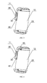
- FIG. 1 is a schematic structural view of a PCB applied to a wireless terminal according to an embodiment of the present invention.
- a wireless terminal may include a PCB 10 and at least two antennas 20, where the PCB 10 includes a resonant component 30 and the PCB 10 is connected to the at least two antennas 20 by using a part of the PCB 10 except for the resonant component 30.
- FIG. 7A is a schematic graph of scattering (Scattering, S) parameters of each antenna of the wireless terminal when the PCB10 does not include the resonant component 30
- FIG. 7B is a schematic graph of S parameters of each antenna of the wireless terminal when the PCB10 includes the resonant component 30.
- S11 indicates a reflection coefficient of an antenna port 1 when an antenna port 2 is matched; S22 indicates a reflection coefficient of the antenna port 2 when the antenna port 1 is matched; and S21 indicates a transmission coefficient from the antenna port 1 to the antenna port 2 when the antenna port 2 is matched.
- isolation that is, S21
- S11 indicates a reflection coefficient of an antenna port 1 when an antenna port 2 is matched; S22 indicates a reflection coefficient of the antenna port 2 when the antenna port 1 is matched; and S21 indicates a transmission coefficient from the antenna port 1 to the antenna port 2 when the antenna port 2 is matched.
- FIG. 8 is a schematic graph of radiation efficiency of each antenna of the wireless terminal.
- the wireless terminal provided in the embodiment of the present invention is simple and easy to implement and has a low cost.
- a first gap 40 is formed on the PCB10, the first gap 40 splits the PCB10 into a first part 11 and a second part 12, the second part 12 is connected to the at least two antennas 20, the second part 12 includes a metal ground, and the first part 11 is connected to the metal ground of the second part 12.
- the first part 11 may be a strip structure at an edge of the PCB10.
- the resonant component 30 may be the first part 11, and a length of the first part 11 may be one fourth of an equivalent wavelength of a resonant frequency band of the resonant component.
- the first part 11 may further be connected to a conductor 80
- the resonant component 30 may be the second part 12 and the conductor 80
- a sum of lengths of the first part 11 and the conductor 80 may be one fourth of the equivalent wavelength of the resonant frequency band of the resonant component.
- an inductor 90 may be further loaded on the first part 11, and the inductor 90 is connected to the metal ground of the second part 12, so that the equivalent wavelength of the resonant frequency band of the resonant component may be shortened, thereby reducing the length of the first part 11 or the sum of lengths of the first part 11 and the conductor 80, and helping reduce the size.
- a second gap 50 is formed on the PCB10, the second gap 50 splits the PCB10 into a third part 13 and a fourth part 14, the fourth part 14 is connected to the at least two antennas 20, the fourth part 14 includes a metal ground, where, a resonant network 130 is loaded on the third part 13.
- the third part 13 may be a strip structure at an edge of the PCB10.
- the resonant network 130 in this embodiment may be specifically a resonant circuit, and the resonant network 130 may be formed by a capacitor C, or a combination of an inductor L and a capacitor C. That is, the resonant network 130 in this embodiment may be implemented by a capacitor, or implemented by a combination of an inductor and a capacitor.
- FIG. 5B is a schematic partial enlarged view of the resonant network 130.
- the PCB10 may have a multi-layer structure; accordingly, a third gap 60 is formed on a first-layer structure 101 of the PCB10, the third gap 60 splits the first-layer structure 101 into a fifth part 15 and a sixth part 16, the sixth part 16 is connected to the at least two antennas 20, and the sixth part 16 includes a metal ground; a fourth gap is formed on a second-layer structure 102 of the PCB10, the fourth gap splits the second-layer structure 102 into a seventh part and an eighth part, the eighth part is connected to the at least two antennas 20, and the eighth part includes a metal ground; and the fifth part 15 and the seventh part have an overlap in a vertical direction of a plane on which the PCB10 resides.
- FIG. 6B is a schematic partial enlarged view of the overlap between the fifth part 15 and the seventh part 17 in the vertical direction of the plane on which the PCB10 resides.
- the fifth part 15 and the seventh part may be respectively a strip structure at an edge of the first-layer structure 101 of the PCB10 and a strip structure at an edge of the second-layer structure 102 of the PCB10.
- first-layer structure 101 of the PCB10 and the second-layer structure 102 of the PCB10 are structures of different layers, which may be structures of two adjacent layers or structures of two non-adjacent layers, and this is not limited herein in the present invention.
- distribution of current on a PCB10 may be changed by resonance current that is generated by a resonant component 30 included in the PCB10, so that isolation between at least two antennas 20 increases.
- electromagnetic radiation capability of the PCB10 may be increased, so that radiation efficiency of each antenna 20 increases, thereby improving wireless performance of a wireless terminal and effectively ensuring wireless performance of the wireless terminal in various application scenarios.
- the wireless terminal provided in the embodiment of the present invention is simple and easy to implement and has a low cost.
- Another embodiment of the present invention provides a wireless terminal, including at least two antennas and the PCB applied to a wireless terminal according to the embodiments corresponding to FIG. 1 to FIG. 8 .
Landscapes
- Engineering & Computer Science (AREA)
- Computer Networks & Wireless Communication (AREA)
- Support Of Aerials (AREA)
- Telephone Set Structure (AREA)
- Details Of Aerials (AREA)
- Transceivers (AREA)
Abstract
Description
- The present invention relates to communications technologies, and in particular, to a printed circuit board (Printed Circuit Board, PCB for short) applied to a wireless terminal and a wireless terminal.
- With rapid development of wireless communications technologies, a multi-antenna technology is more and more widely applied to various wireless terminals, such as a user equipment (User Equipment, UE) in a Long Term Evolution (Long Term Evolution, LTE for short) system or a Worldwide Interoperability for Microwave Access (Worldwide Interoperability for Microwave Access, WIMAX for short) system. The multi-antenna technology means that multiple antennas are used both at a transmit end and at a receive end to send or receive a signal, that is, a multi-antenna system using the multi-antenna technology includes multiple transmit channels and multiple receive channels.
- However, because a spacing between multiple antennas of a wireless terminal is relatively small and operating frequency bands are overlapped, the multiple antennas affect each other, causing a decrease in isolation between at least two antennas and a decrease in radiation efficiency of each antenna, thereby lowering wireless performance of the wireless terminal.
- In multiple aspects of the present invention, a PCB applied to a wireless terminal and a wireless terminal are provided to improve wireless performance of the wireless terminal.
- In one aspect of the present invention, a PCB applied to a wireless terminal is provided, where the PCB includes a resonant component and the PCB is connected to at least two antennas of the wireless terminal by using a part of the PCB except for the resonant component.
- With reference to the foregoing aspect and any possible implementation manner, an implementation manner is further provided, where a first gap is formed on the PCB, the first gap splits the PCB into a first part and a second part, the second part is connected to the at least two antennas, the second part includes a metal ground, and the first part is connected to the metal ground of the second part, where,
the resonant component is the first part, and a length of the first part is one fourth of an equivalent wavelength of a resonant frequency band of the resonant component; or
the first part is connected to a conductor, the resonant component is the first part and the conductor, and a sum of lengths of the first part and the conductor is one fourth of an equivalent wavelength of a resonant frequency band of the resonant component. - With reference to the foregoing aspect and any possible implementation manner, an implementation manner is further provided, where an inductor is loaded on the first part, and the inductor is connected to the metal ground of the second part.
- With reference to the foregoing aspect and any possible implementation manner, an implementation manner is further provided, where a second gap is formed on the PCB, the second gap splits the PCB into a third part and a fourth part, the fourth part is connected to the at least two antennas, the fourth part includes a metal ground, and the third part is connected to the metal ground of the fourth part, where a resonant network is loaded on the third part.
- With reference to the foregoing aspect and any possible implementation manner, an implementation manner is further provided, where the resonant network is formed by a capacitor, or an inductor and a capacitor.
- With reference to the foregoing aspect and any possible implementation manner, an implementation manner is further provided, where the PCB has a multi-layer structure;
a third gap is formed on a first-layer structure of the PCB, the third gap splits the first-layer structure into a fifth part and a sixth part, the sixth part is connected to the at least two antennas, the sixth part includes a metal ground, and the fifth part is connected to the metal ground of the sixth part;
a fourth gap is formed on a second-layer structure of the PCB, the fourth gap splits the second-layer structure into a seventh part and an eighth part, the eighth part is connected to the at least two antennas, the eighth part includes a metal ground, and the seventh part is connected to the metal ground of the eighth part; and
the fifth part and the seventh part have an overlap in a vertical direction of a plane on which the PCB resides. - In another aspect of the present invention, a wireless terminal is provided, including at least two antennas and the PCB applied to a wireless terminal according to the following aspect and any possible implementation manner.
- As can be seen from the foregoing technical solutions, in embodiments of the present invention, distribution of current on a PCB may be changed by resonance current that is generated by a resonant component included in the PCB, so that isolation between at least two antennas increases. In addition, due to existence of the resonance current, electromagnetic radiation capability of the PCB may be increased, so that radiation efficiency of each antenna increases, thereby improving wireless performance of a wireless terminal and effectively ensuring wireless performance of the wireless terminal in various application scenarios. Furthermore, the wireless terminal provided in the embodiments of the present invention is simple and easy to implement and has a low cost.
- To illustrate the technical solutions in the embodiments of the present invention or in the prior art more clearly, the following briefly introduces the accompanying drawings required for describing the embodiments or the prior art. Apparently, the accompanying drawings in the following description show merely some embodiments of the present invention, and a person of ordinary skill in the art may still derive other drawings from these accompanying drawings without creative efforts.
-
FIG. 1 is a schematic structural view of a PCB applied to a wireless terminal according to an embodiment of the present invention; -
FIG. 2 is a schematic structural view of a PCB applied to a wireless terminal according to another embodiment of the present invention; -
FIG. 3 is a schematic structural view of a PCB applied to a wireless terminal according to another embodiment of the present invention; -
FIG. 4 is a schematic structural view of a PCB applied to a wireless terminal according to another embodiment of the present invention; -
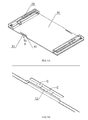
FIG. 5A is a schematic structural view of a PCB applied to a wireless terminal according to another embodiment of the present invention; -
FIG. 5B is a schematic partial enlarged view of the resonant network 130 according to the embodiment corresponding toFIG. 5A ; -
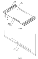
FIG. 6A is a schematic structural view of a PCB applied to a wireless terminal according to another embodiment of the present invention; -
FIG. 6B is a schematic partial enlarged view of an overlap between thefifth part 15 and theseventh part 17 in a vertical direction of a plane on which the PCB10 resides according to the embodiment corresponding toFIG. 6A ; -
FIG. 7A is a schematic graph of S parameters of each antenna of a wireless terminal using the PCB10 that does not include aresonant component 30; -
FIG. 7B is a schematic graph of S parameters of each antenna of a wireless terminal using the PCB10 that includes aresonant component 30; and -
FIG. 8 is a schematic graph of radiation efficiency of each antenna of the wireless terminal. - To make the objectives, technical solutions, and advantages of the embodiments of the present invention more comprehensible, the following clearly and completely describes the technical solutions in the embodiments of the present invention with reference to the accompanying drawings in the embodiments of the present invention. Apparently, the described embodiments are merely a part rather than all of the embodiments of the present invention. All other embodiments obtained by a person of ordinary skill in the art based on the embodiments of the present invention without creative efforts shall fall within the protection scope of the present invention.
- The wireless terminal according to an embodiment of the present invention may include but is not limited to a mobile phone, a data card, or a machine-to-machine (Machine to Machine, M2M for short) wireless module.
- In addition, the term "and/or" in this specification is used only to describe an association relationship between associated objects and indicates that three relationships may exist. For example, "A and/or B" may indicate the following three cases: A separately exists, A and B simultaneously exist, and B separately exists. In addition, generally the symbol "/" in this specification indicates an "or" relationship between associated objects before and after the symbol.
- The present invention provides a PCB applied to a wireless terminal and a wireless terminal, where: the wireless terminal may include a printed circuit board (Printed Circuit Board, PCB for short) and at least two antennas, the PCB includes a resonant component, and the PCB is connected to the at least two antennas by using a part of the PCB except for the resonant component. Since distribution of current on the PCB may be changed by resonance current that is generated by the resonant component, isolation between the at least two antennas increases. In addition, due to existence of the resonance current, electromagnetic radiation capability of the PCB may be increased, so that radiation efficiency of each antenna increases, thereby improving wireless performance of the wireless terminal and effectively ensuring wireless performance of the wireless terminal in various application scenarios. Furthermore, the wireless terminal provided in the embodiment of the present invention is simple and easy to implement and has a low cost.
- Optionally, in a possible implementation manner of this embodiment, a first gap is formed on the PCB, the first gap splits the PCB into a first part and a second part, the second part is connected to the at least two antennas, the second part includes a metal ground, and the first part is connected to the metal ground of the second part.
- Specifically, the resonant component may be the first part, and a length of the first part may be one fourth of an equivalent wavelength of a resonant frequency band of the resonant component.
- Specifically, the first part may further be connected to a conductor, the resonant component may be the first part and the conductor, and a sum of lengths of the first part and the conductor may be one fourth of the equivalent wavelength of the resonant frequency band of the resonant component.
- Optionally, an inductor may be further loaded on the first part, and the inductor is connected to the metal ground of the second part, so that the equivalent wavelength of the resonant frequency band of the resonant component may be shortened, thereby reducing the length of the first part or the sum of lengths of the first part and the conductor, and helping reduce the size.
- Optionally, in a possible implementation manner of this embodiment, a second gap is formed on the PCB, the second gap splits the PCB into a third part and a fourth part, the fourth part is connected to the at least two antennas, the fourth part includes a metal ground, where a resonant network is loaded on the third part.
- Specifically, the resonant network in this embodiment may be specifically a resonant circuit, and the resonant network may be formed by a capacitor C, or a combination of an inductor L and a capacitor C. That is, the resonant network in this embodiment may be implemented by a capacitor, or implemented by a combination of an inductor and a capacitor.
- Optionally, in a possible implementation manner of this embodiment, the PCB may have a multi-layer structure; accordingly, a third gap is formed on a first-layer structure of the PCB, the third gap splits the first-layer structure into a fifth part and a sixth part, the sixth part is connected to the at least two antennas, and the sixth part includes a metal ground; a fourth gap is formed on a second-layer structure of the PCB, the fourth gap splits the second-layer structure into a seventh part and an eighth part, the eighth part is connected to the at least two antennas, and the eighth part includes a metal ground; and the fifth part and the seventh part have an overlap in a vertical direction of a plane on which the PCB resides.
- It should be noted that the first-layer structure of the PCB and the second-layer structure of the PCB are structures of different layers, which may be structures of two adjacent layers or structures of two non-adjacent layers, and this is not limited herein in the present invention.
- In the present invention, distribution of current on a PCB may be changed by resonance current that is generated by a resonant component included in the PCB, so that isolation between at least two antennas increases. In addition, due to existence of the resonance current, electromagnetic radiation capability of the PCB may be increased, so that radiation efficiency of each antenna increases, thereby improving wireless performance of a wireless terminal and effectively ensuring wireless performance of the wireless terminal in various application scenarios. Furthermore, the wireless terminal provided in the embodiment of the present invention is simple and easy to implement and has a low cost.
-
FIG. 1 is a schematic structural view of a PCB applied to a wireless terminal according to an embodiment of the present invention. As shown inFIG. 1 , a wireless terminal may include aPCB 10 and at least twoantennas 20, where thePCB 10 includes aresonant component 30 and thePCB 10 is connected to the at least twoantennas 20 by using a part of thePCB 10 except for theresonant component 30. - Since distribution of current on the PCB10 may be changed by resonance current that is generated by the
resonant component 30, isolation between the at least twoantennas 20 increases. Taking a dual-antenna wireless terminal as an example,FIG. 7A is a schematic graph of scattering (Scattering, S) parameters of each antenna of the wireless terminal when the PCB10 does not include theresonant component 30, andFIG. 7B is a schematic graph of S parameters of each antenna of the wireless terminal when the PCB10 includes theresonant component 30. S11 indicates a reflection coefficient of anantenna port 1 when anantenna port 2 is matched; S22 indicates a reflection coefficient of theantenna port 2 when theantenna port 1 is matched; and S21 indicates a transmission coefficient from theantenna port 1 to theantenna port 2 when theantenna port 2 is matched. As can be seen, although isolation, that is, S21, increases, radiation efficiency, that is, S11, of the antenna is not obviously affected. Generally, a smaller S11 indicates less energy reflected back and more energy radiated outward. In this case, S11 may indicate that the radiation efficiency of the antenna is much higher. Therefore, generally S11 is used to roughly determine the radiation efficiency of the antenna. - In addition, due to existence of the resonance current, electromagnetic radiation capability of the
PCB 10 may be increased, so that radiation efficiency of eachantenna 20 increases, thereby improving wireless performance of the wireless terminal and effectively ensuring wireless performance of the wireless terminal in various application scenarios. Taking a dual-antenna wireless terminal as an example,FIG. 8 is a schematic graph of radiation efficiency of each antenna of the wireless terminal. - Furthermore, the wireless terminal provided in the embodiment of the present invention is simple and easy to implement and has a low cost.
- Optionally, in a possible implementation manner of this embodiment, as shown in
FIG. 2 , afirst gap 40 is formed on the PCB10, thefirst gap 40 splits the PCB10 into afirst part 11 and asecond part 12, thesecond part 12 is connected to the at least twoantennas 20, thesecond part 12 includes a metal ground, and thefirst part 11 is connected to the metal ground of thesecond part 12. - Preferably, the
first part 11 may be a strip structure at an edge of the PCB10. - Specifically, the
resonant component 30 may be thefirst part 11, and a length of thefirst part 11 may be one fourth of an equivalent wavelength of a resonant frequency band of the resonant component. - Specifically, as shown in
FIG. 3 , thefirst part 11 may further be connected to aconductor 80, theresonant component 30 may be thesecond part 12 and theconductor 80, and a sum of lengths of thefirst part 11 and theconductor 80 may be one fourth of the equivalent wavelength of the resonant frequency band of the resonant component. - Optionally, as shown in
FIG. 4 , aninductor 90 may be further loaded on thefirst part 11, and theinductor 90 is connected to the metal ground of thesecond part 12, so that the equivalent wavelength of the resonant frequency band of the resonant component may be shortened, thereby reducing the length of thefirst part 11 or the sum of lengths of thefirst part 11 and theconductor 80, and helping reduce the size. - Optionally, in a possible implementation manner of this embodiment, as shown in
FIG. 5A , asecond gap 50 is formed on the PCB10, thesecond gap 50 splits the PCB10 into athird part 13 and afourth part 14, thefourth part 14 is connected to the at least twoantennas 20, thefourth part 14 includes a metal ground, where, a resonant network 130 is loaded on thethird part 13. - Preferably, the
third part 13 may be a strip structure at an edge of the PCB10. - Specifically, the resonant network 130 in this embodiment may be specifically a resonant circuit, and the resonant network 130 may be formed by a capacitor C, or a combination of an inductor L and a capacitor C. That is, the resonant network 130 in this embodiment may be implemented by a capacitor, or implemented by a combination of an inductor and a capacitor.
FIG. 5B is a schematic partial enlarged view of the resonant network 130. - Optionally, in a possible implementation manner of this embodiment, as shown in
FIG. 6A , the PCB10 may have a multi-layer structure; accordingly, athird gap 60 is formed on a first-layer structure 101 of the PCB10, thethird gap 60 splits the first-layer structure 101 into afifth part 15 and asixth part 16, thesixth part 16 is connected to the at least twoantennas 20, and thesixth part 16 includes a metal ground; a fourth gap is formed on a second-layer structure 102 of the PCB10, the fourth gap splits the second-layer structure 102 into a seventh part and an eighth part, the eighth part is connected to the at least twoantennas 20, and the eighth part includes a metal ground; and thefifth part 15 and the seventh part have an overlap in a vertical direction of a plane on which the PCB10 resides. - Since the
fifth part 15 and the seventh part have an overlap in the vertical direction of the plane on which the PCB10 resides, a capacitance effect can be formed.FIG. 6B is a schematic partial enlarged view of the overlap between thefifth part 15 and theseventh part 17 in the vertical direction of the plane on which the PCB10 resides. - Preferably, the
fifth part 15 and the seventh part may be respectively a strip structure at an edge of the first-layer structure 101 of the PCB10 and a strip structure at an edge of the second-layer structure 102 of the PCB10. - It should be noted that the first-layer structure 101 of the PCB10 and the second-layer structure 102 of the PCB10 are structures of different layers, which may be structures of two adjacent layers or structures of two non-adjacent layers, and this is not limited herein in the present invention.
- In this embodiment, distribution of current on a PCB10 may be changed by resonance current that is generated by a
resonant component 30 included in the PCB10, so that isolation between at least twoantennas 20 increases. In addition, due to existence of the resonance current, electromagnetic radiation capability of the PCB10 may be increased, so that radiation efficiency of eachantenna 20 increases, thereby improving wireless performance of a wireless terminal and effectively ensuring wireless performance of the wireless terminal in various application scenarios. Furthermore, the wireless terminal provided in the embodiment of the present invention is simple and easy to implement and has a low cost. - Another embodiment of the present invention provides a wireless terminal, including at least two antennas and the PCB applied to a wireless terminal according to the embodiments corresponding to
FIG. 1 to FIG. 8 . - It should be noted that "first", "second", and the like in the embodiments are intended to differentiate each functional component rather than representing a sequence of components.
- Finally, it should be noted that the foregoing embodiments are merely intended for describing the technical solutions of the present invention rather than limiting the present invention. Although the present invention is described in detail with reference to the foregoing embodiments, a person of ordinary skill in the art should understand that he may still make modifications to the technical solutions described in the foregoing embodiments, or make equivalent replacements to some technical features thereof, as long as such modifications or replacements do not cause the essence of corresponding technical solutions to depart from the scope of the technical solutions of the embodiments of the present invention.
Claims (7)
- A PCB applied to a wireless terminal, wherein the PCB comprises a resonant component and the PCB is connected to at least two antennas of the wireless terminal by using a part of the PCB except for the resonant component.
- The PCB applied to a wireless terminal according to claim 1, wherein a first gap is formed on the PCB, the first gap splits the PCB into a first part and a second part, the second part is connected to the at least two antennas, the second part comprises a metal ground, and the first part is connected to the metal ground of the second part, wherein,
the resonant component is the first part, and a length of the first part is one fourth of an equivalent wavelength of a resonant frequency band of the resonant component; or
the first part is connected to a conductor, the resonant component is the first part and the conductor, and a sum of lengths of the first part and the conductor is one fourth of an equivalent wavelength of a resonant frequency band of the resonant component. - The PCB applied to a wireless terminal according to claim 2, wherein an inductor is loaded on the first part, and the inductor is connected to the metal ground of the second part.
- The PCB applied to a wireless terminal according to claim 1, wherein a second gap is formed on the PCB, the second gap splits the PCB into a third part and a fourth part, the fourth part is connected to the at least two antennas, the fourth part comprises a metal ground, and the third part is connected to the metal ground of the fourth part; and a resonant network is loaded on the third part.
- The PCB applied to a wireless terminal according to claim 4, wherein the resonant network is formed by a capacitor, or an inductor and a capacitor.
- The PCB applied to a wireless terminal according to claim 1, wherein the PCB has a multi-layer structure;
a third gap is formed on a first-layer structure of the PCB, the third gap splits the first-layer structure into a fifth part and a sixth part, the sixth part is connected to the at least two antennas, the sixth part comprises a metal ground, and the fifth part is connected to the metal ground of the sixth part;
a fourth gap is formed on a second-layer structure of the PCB, the fourth gap splits the second-layer structure into a seventh part and an eighth part, the eighth part is connected to the at least two antennas, the eighth part comprises a metal ground, and the seventh part is connected to the metal ground of the eighth part; and
the fifth part and the seventh part have an overlap in a vertical direction of a plane on which the PCB resides. - A wireless terminal, comprising at least two antennas and the PCB applied to a wireless terminal according to any one of claims 1 to 6.
Applications Claiming Priority (1)
| Application Number | Priority Date | Filing Date | Title |
|---|---|---|---|
| PCT/CN2012/086154 WO2014086034A1 (en) | 2012-12-07 | 2012-12-07 | Pcb applied in wireless terminal and wireless terminal |
Publications (3)
| Publication Number | Publication Date |
|---|---|
| EP2760079A1 true EP2760079A1 (en) | 2014-07-30 |
| EP2760079A4 EP2760079A4 (en) | 2015-02-25 |
| EP2760079B1 EP2760079B1 (en) | 2018-08-29 |
Family
ID=50323352
Family Applications (1)
| Application Number | Title | Priority Date | Filing Date |
|---|---|---|---|
| EP12877079.9A Not-in-force EP2760079B1 (en) | 2012-12-07 | 2012-12-07 | Pcb applied in wireless terminal and wireless terminal |
Country Status (5)
| Country | Link |
|---|---|
| US (1) | US20140159981A1 (en) |
| EP (1) | EP2760079B1 (en) |
| JP (1) | JP2015509318A (en) |
| CN (1) | CN103688599B (en) |
| WO (1) | WO2014086034A1 (en) |
Families Citing this family (7)
| Publication number | Priority date | Publication date | Assignee | Title |
|---|---|---|---|---|
| US9799953B2 (en) | 2015-03-26 | 2017-10-24 | Microsoft Technology Licensing, Llc | Antenna isolation |
| US10498030B2 (en) * | 2016-06-27 | 2019-12-03 | Intel IP Corporation | Frequency reconfigurable antenna decoupling for wireless communication |
| JP6865074B2 (en) * | 2017-03-14 | 2021-04-28 | 株式会社パナソニックシステムネットワークス開発研究所 | Antenna device and electronic device equipped with an antenna device |
| CN111771305B (en) | 2018-04-05 | 2021-11-26 | 华为技术有限公司 | Antenna arrangement with wave trap and user equipment |
| US10957985B2 (en) | 2018-09-28 | 2021-03-23 | Apple Inc. | Electronic devices having antenna module isolation structures |
| CN113809522B (en) * | 2021-09-10 | 2023-11-07 | Oppo广东移动通信有限公司 | Antenna assembly and electronic equipment |
| TWI793867B (en) * | 2021-11-19 | 2023-02-21 | 啓碁科技股份有限公司 | Communication device |
Family Cites Families (17)
| Publication number | Priority date | Publication date | Assignee | Title |
|---|---|---|---|---|
| US6686886B2 (en) * | 2001-05-29 | 2004-02-03 | International Business Machines Corporation | Integrated antenna for laptop applications |
| JP4091897B2 (en) * | 2003-10-23 | 2008-05-28 | 松下電器産業株式会社 | Portable radio |
| JP2006074446A (en) * | 2004-09-02 | 2006-03-16 | Ngk Spark Plug Co Ltd | ANTENNA DEVICE, WIRELESS COMMUNICATION DEVICE USING THE SAME, AND METHOD FOR MANUFACTURING ANTENNA DEVICE |
| EP1843432B1 (en) * | 2005-01-27 | 2015-08-12 | Murata Manufacturing Co., Ltd. | Antenna and wireless communication device |
| US7417591B2 (en) * | 2005-02-17 | 2008-08-26 | Matsushita Electric Industrial Co., Ltd. | Antenna apparatus and portable wireless device using the same |
| JP2006229528A (en) * | 2005-02-17 | 2006-08-31 | Matsushita Electric Ind Co Ltd | Antenna device and portable radio using the same |
| JP4804447B2 (en) * | 2006-12-05 | 2011-11-02 | パナソニック株式会社 | ANTENNA DEVICE AND WIRELESS COMMUNICATION DEVICE |
| CN201345425Y (en) * | 2008-09-27 | 2009-11-11 | 耀登科技股份有限公司 | Double-frequency space diversity double-antenna for mobile terminal |
| KR101051911B1 (en) * | 2009-02-17 | 2011-07-26 | 주식회사 이엠따블유 | MIO antenna system including isolation configured using metamaterial |
| US8339322B2 (en) * | 2009-02-19 | 2012-12-25 | Galtronics Corporation Ltd. | Compact multi-band antennas |
| KR101119603B1 (en) * | 2009-12-22 | 2012-03-06 | 주식회사 이엠따블유 | Apparatus for antenna |
| JP5431200B2 (en) * | 2010-02-10 | 2014-03-05 | シャープ株式会社 | Circuit board and electronic device including the circuit board |
| JP2012039465A (en) * | 2010-08-09 | 2012-02-23 | Panasonic Corp | Portable radio device |
| JP5652133B2 (en) * | 2010-11-01 | 2015-01-14 | 船井電機株式会社 | Multi-antenna device and portable device |
| JP2012105125A (en) * | 2010-11-11 | 2012-05-31 | Nec Casio Mobile Communications Ltd | Antenna for mobile terminal and method of manufacturing the same |
| US9203139B2 (en) * | 2012-05-04 | 2015-12-01 | Apple Inc. | Antenna structures having slot-based parasitic elements |
| US8922448B2 (en) * | 2012-09-26 | 2014-12-30 | Mediatek Singapore Pte. Ltd. | Communication device and antennas with high isolation characteristics |
-
2012
- 2012-12-07 JP JP2014550618A patent/JP2015509318A/en active Pending
- 2012-12-07 EP EP12877079.9A patent/EP2760079B1/en not_active Not-in-force
- 2012-12-07 CN CN201280007739.4A patent/CN103688599B/en active Active
- 2012-12-07 WO PCT/CN2012/086154 patent/WO2014086034A1/en not_active Ceased
-
2013
- 2013-12-30 US US14/143,896 patent/US20140159981A1/en not_active Abandoned
Also Published As
| Publication number | Publication date |
|---|---|
| CN103688599A (en) | 2014-03-26 |
| US20140159981A1 (en) | 2014-06-12 |
| WO2014086034A1 (en) | 2014-06-12 |
| CN103688599B (en) | 2017-06-20 |
| EP2760079B1 (en) | 2018-08-29 |
| EP2760079A4 (en) | 2015-02-25 |
| JP2015509318A (en) | 2015-03-26 |
Similar Documents
| Publication | Publication Date | Title |
|---|---|---|
| US10819031B2 (en) | Printed circuit board antenna and terminal | |
| EP2760079B1 (en) | Pcb applied in wireless terminal and wireless terminal | |
| US9077084B2 (en) | Multi-band multi-antenna system and communication device thereof | |
| KR102272966B1 (en) | Capacitively-coupled isolator assembly | |
| US9825366B2 (en) | Printed circuit board antenna and printed circuit board | |
| EP4220857A2 (en) | Antenna and mobile terminal | |
| US10177463B2 (en) | Antenna system and electronic apparatus | |
| US9680222B2 (en) | Antenna structure and wireless communication device using the same | |
| EP3300170B1 (en) | Antenna and user equipment | |
| US9819091B2 (en) | Portable terminal and slot antenna thereof | |
| EP2894717B1 (en) | Antenna | |
| US20160087667A1 (en) | Wireless Communications Device | |
| EP2562868A1 (en) | A multiple-turn loop antenna arrangement and a portable radio communication device comprising such an arrangement | |
| Chen et al. | Low‐profile, small‐size, wireless wide area network handset antenna close integration with surrounding ground plane | |
| US20140340277A1 (en) | Communication device and antenna element therein | |
| US20250105510A1 (en) | Antenna and electronic device |
Legal Events
| Date | Code | Title | Description |
|---|---|---|---|
| PUAI | Public reference made under article 153(3) epc to a published international application that has entered the european phase |
Free format text: ORIGINAL CODE: 0009012 |
|
| 17P | Request for examination filed |
Effective date: 20131122 |
|
| AK | Designated contracting states |
Kind code of ref document: A1 Designated state(s): AL AT BE BG CH CY CZ DE DK EE ES FI FR GB GR HR HU IE IS IT LI LT LU LV MC MK MT NL NO PL PT RO RS SE SI SK SM TR |
|
| A4 | Supplementary search report drawn up and despatched |
Effective date: 20150122 |
|
| RIC1 | Information provided on ipc code assigned before grant |
Ipc: H01Q 1/48 20060101ALI20150116BHEP Ipc: H01Q 21/28 20060101ALI20150116BHEP Ipc: H01Q 9/04 20060101ALI20150116BHEP Ipc: H01Q 1/24 20060101ALI20150116BHEP Ipc: H01Q 1/52 20060101AFI20150116BHEP |
|
| 17Q | First examination report despatched |
Effective date: 20151202 |
|
| DAX | Request for extension of the european patent (deleted) | ||
| RAP1 | Party data changed (applicant data changed or rights of an application transferred) |
Owner name: HUAWEI DEVICE (DONGGUAN) CO., LTD. |
|
| GRAP | Despatch of communication of intention to grant a patent |
Free format text: ORIGINAL CODE: EPIDOSNIGR1 |
|
| INTG | Intention to grant announced |
Effective date: 20180316 |
|
| RIN1 | Information on inventor provided before grant (corrected) |
Inventor name: WANG, HANYANG |
|
| GRAS | Grant fee paid |
Free format text: ORIGINAL CODE: EPIDOSNIGR3 |
|
| GRAA | (expected) grant |
Free format text: ORIGINAL CODE: 0009210 |
|
| AK | Designated contracting states |
Kind code of ref document: B1 Designated state(s): AL AT BE BG CH CY CZ DE DK EE ES FI FR GB GR HR HU IE IS IT LI LT LU LV MC MK MT NL NO PL PT RO RS SE SI SK SM TR |
|
| REG | Reference to a national code |
Ref country code: GB Ref legal event code: FG4D |
|
| REG | Reference to a national code |
Ref country code: CH Ref legal event code: EP |
|
| REG | Reference to a national code |
Ref country code: AT Ref legal event code: REF Ref document number: 1036249 Country of ref document: AT Kind code of ref document: T Effective date: 20180915 |
|
| REG | Reference to a national code |
Ref country code: IE Ref legal event code: FG4D |
|
| REG | Reference to a national code |
Ref country code: DE Ref legal event code: R096 Ref document number: 602012050516 Country of ref document: DE |
|
| REG | Reference to a national code |
Ref country code: NL Ref legal event code: FP |
|
| REG | Reference to a national code |
Ref country code: LT Ref legal event code: MG4D |
|
| PG25 | Lapsed in a contracting state [announced via postgrant information from national office to epo] |
Ref country code: LT Free format text: LAPSE BECAUSE OF FAILURE TO SUBMIT A TRANSLATION OF THE DESCRIPTION OR TO PAY THE FEE WITHIN THE PRESCRIBED TIME-LIMIT Effective date: 20180829 Ref country code: GR Free format text: LAPSE BECAUSE OF FAILURE TO SUBMIT A TRANSLATION OF THE DESCRIPTION OR TO PAY THE FEE WITHIN THE PRESCRIBED TIME-LIMIT Effective date: 20181130 Ref country code: SE Free format text: LAPSE BECAUSE OF FAILURE TO SUBMIT A TRANSLATION OF THE DESCRIPTION OR TO PAY THE FEE WITHIN THE PRESCRIBED TIME-LIMIT Effective date: 20180829 Ref country code: BG Free format text: LAPSE BECAUSE OF FAILURE TO SUBMIT A TRANSLATION OF THE DESCRIPTION OR TO PAY THE FEE WITHIN THE PRESCRIBED TIME-LIMIT Effective date: 20181129 Ref country code: RS Free format text: LAPSE BECAUSE OF FAILURE TO SUBMIT A TRANSLATION OF THE DESCRIPTION OR TO PAY THE FEE WITHIN THE PRESCRIBED TIME-LIMIT Effective date: 20180829 Ref country code: IS Free format text: LAPSE BECAUSE OF FAILURE TO SUBMIT A TRANSLATION OF THE DESCRIPTION OR TO PAY THE FEE WITHIN THE PRESCRIBED TIME-LIMIT Effective date: 20181229 Ref country code: NO Free format text: LAPSE BECAUSE OF FAILURE TO SUBMIT A TRANSLATION OF THE DESCRIPTION OR TO PAY THE FEE WITHIN THE PRESCRIBED TIME-LIMIT Effective date: 20181129 Ref country code: FI Free format text: LAPSE BECAUSE OF FAILURE TO SUBMIT A TRANSLATION OF THE DESCRIPTION OR TO PAY THE FEE WITHIN THE PRESCRIBED TIME-LIMIT Effective date: 20180829 |
|
| REG | Reference to a national code |
Ref country code: AT Ref legal event code: MK05 Ref document number: 1036249 Country of ref document: AT Kind code of ref document: T Effective date: 20180829 |
|
| PG25 | Lapsed in a contracting state [announced via postgrant information from national office to epo] |
Ref country code: LV Free format text: LAPSE BECAUSE OF FAILURE TO SUBMIT A TRANSLATION OF THE DESCRIPTION OR TO PAY THE FEE WITHIN THE PRESCRIBED TIME-LIMIT Effective date: 20180829 Ref country code: AL Free format text: LAPSE BECAUSE OF FAILURE TO SUBMIT A TRANSLATION OF THE DESCRIPTION OR TO PAY THE FEE WITHIN THE PRESCRIBED TIME-LIMIT Effective date: 20180829 Ref country code: HR Free format text: LAPSE BECAUSE OF FAILURE TO SUBMIT A TRANSLATION OF THE DESCRIPTION OR TO PAY THE FEE WITHIN THE PRESCRIBED TIME-LIMIT Effective date: 20180829 |
|
| PG25 | Lapsed in a contracting state [announced via postgrant information from national office to epo] |
Ref country code: AT Free format text: LAPSE BECAUSE OF FAILURE TO SUBMIT A TRANSLATION OF THE DESCRIPTION OR TO PAY THE FEE WITHIN THE PRESCRIBED TIME-LIMIT Effective date: 20180829 Ref country code: EE Free format text: LAPSE BECAUSE OF FAILURE TO SUBMIT A TRANSLATION OF THE DESCRIPTION OR TO PAY THE FEE WITHIN THE PRESCRIBED TIME-LIMIT Effective date: 20180829 Ref country code: RO Free format text: LAPSE BECAUSE OF FAILURE TO SUBMIT A TRANSLATION OF THE DESCRIPTION OR TO PAY THE FEE WITHIN THE PRESCRIBED TIME-LIMIT Effective date: 20180829 Ref country code: IT Free format text: LAPSE BECAUSE OF FAILURE TO SUBMIT A TRANSLATION OF THE DESCRIPTION OR TO PAY THE FEE WITHIN THE PRESCRIBED TIME-LIMIT Effective date: 20180829 Ref country code: CZ Free format text: LAPSE BECAUSE OF FAILURE TO SUBMIT A TRANSLATION OF THE DESCRIPTION OR TO PAY THE FEE WITHIN THE PRESCRIBED TIME-LIMIT Effective date: 20180829 Ref country code: PL Free format text: LAPSE BECAUSE OF FAILURE TO SUBMIT A TRANSLATION OF THE DESCRIPTION OR TO PAY THE FEE WITHIN THE PRESCRIBED TIME-LIMIT Effective date: 20180829 Ref country code: ES Free format text: LAPSE BECAUSE OF FAILURE TO SUBMIT A TRANSLATION OF THE DESCRIPTION OR TO PAY THE FEE WITHIN THE PRESCRIBED TIME-LIMIT Effective date: 20180829 |
|
| PG25 | Lapsed in a contracting state [announced via postgrant information from national office to epo] |
Ref country code: DK Free format text: LAPSE BECAUSE OF FAILURE TO SUBMIT A TRANSLATION OF THE DESCRIPTION OR TO PAY THE FEE WITHIN THE PRESCRIBED TIME-LIMIT Effective date: 20180829 Ref country code: SM Free format text: LAPSE BECAUSE OF FAILURE TO SUBMIT A TRANSLATION OF THE DESCRIPTION OR TO PAY THE FEE WITHIN THE PRESCRIBED TIME-LIMIT Effective date: 20180829 Ref country code: SK Free format text: LAPSE BECAUSE OF FAILURE TO SUBMIT A TRANSLATION OF THE DESCRIPTION OR TO PAY THE FEE WITHIN THE PRESCRIBED TIME-LIMIT Effective date: 20180829 |
|
| REG | Reference to a national code |
Ref country code: DE Ref legal event code: R097 Ref document number: 602012050516 Country of ref document: DE |
|
| REG | Reference to a national code |
Ref country code: NL Ref legal event code: HC Owner name: HUAWEI DEVICE CO., LTD.; CN Free format text: DETAILS ASSIGNMENT: CHANGE OF OWNER(S), CHANGE OF OWNER(S) NAME; FORMER OWNER NAME: HUAWEI DEVICE (DONGGUAN) CO., LTD. Effective date: 20190514 |
|
| RAP2 | Party data changed (patent owner data changed or rights of a patent transferred) |
Owner name: HUAWEI DEVICE CO., LTD. |
|
| REG | Reference to a national code |
Ref country code: DE Ref legal event code: R081 Ref document number: 602012050516 Country of ref document: DE Owner name: HUAWEI DEVICE CO., LTD., DONGGUAN, CN Free format text: FORMER OWNER: HUAWEI DEVICE (DONGGUAN) CO., LTD., DONGGUAN, GUANGDONG, CN |
|
| PLBE | No opposition filed within time limit |
Free format text: ORIGINAL CODE: 0009261 |
|
| STAA | Information on the status of an ep patent application or granted ep patent |
Free format text: STATUS: NO OPPOSITION FILED WITHIN TIME LIMIT |
|
| REG | Reference to a national code |
Ref country code: CH Ref legal event code: PL |
|
| 26N | No opposition filed |
Effective date: 20190531 |
|
| PG25 | Lapsed in a contracting state [announced via postgrant information from national office to epo] |
Ref country code: MC Free format text: LAPSE BECAUSE OF FAILURE TO SUBMIT A TRANSLATION OF THE DESCRIPTION OR TO PAY THE FEE WITHIN THE PRESCRIBED TIME-LIMIT Effective date: 20180829 Ref country code: LU Free format text: LAPSE BECAUSE OF NON-PAYMENT OF DUE FEES Effective date: 20181207 Ref country code: SI Free format text: LAPSE BECAUSE OF FAILURE TO SUBMIT A TRANSLATION OF THE DESCRIPTION OR TO PAY THE FEE WITHIN THE PRESCRIBED TIME-LIMIT Effective date: 20180829 |
|
| REG | Reference to a national code |
Ref country code: IE Ref legal event code: MM4A |
|
| REG | Reference to a national code |
Ref country code: BE Ref legal event code: MM Effective date: 20181231 |
|
| PG25 | Lapsed in a contracting state [announced via postgrant information from national office to epo] |
Ref country code: IE Free format text: LAPSE BECAUSE OF NON-PAYMENT OF DUE FEES Effective date: 20181207 |
|
| PG25 | Lapsed in a contracting state [announced via postgrant information from national office to epo] |
Ref country code: BE Free format text: LAPSE BECAUSE OF NON-PAYMENT OF DUE FEES Effective date: 20181231 |
|
| PG25 | Lapsed in a contracting state [announced via postgrant information from national office to epo] |
Ref country code: CH Free format text: LAPSE BECAUSE OF NON-PAYMENT OF DUE FEES Effective date: 20181231 Ref country code: LI Free format text: LAPSE BECAUSE OF NON-PAYMENT OF DUE FEES Effective date: 20181231 |
|
| PG25 | Lapsed in a contracting state [announced via postgrant information from national office to epo] |
Ref country code: MT Free format text: LAPSE BECAUSE OF NON-PAYMENT OF DUE FEES Effective date: 20181207 |
|
| PG25 | Lapsed in a contracting state [announced via postgrant information from national office to epo] |
Ref country code: TR Free format text: LAPSE BECAUSE OF FAILURE TO SUBMIT A TRANSLATION OF THE DESCRIPTION OR TO PAY THE FEE WITHIN THE PRESCRIBED TIME-LIMIT Effective date: 20180829 |
|
| PG25 | Lapsed in a contracting state [announced via postgrant information from national office to epo] |
Ref country code: PT Free format text: LAPSE BECAUSE OF FAILURE TO SUBMIT A TRANSLATION OF THE DESCRIPTION OR TO PAY THE FEE WITHIN THE PRESCRIBED TIME-LIMIT Effective date: 20180829 |
|
| PG25 | Lapsed in a contracting state [announced via postgrant information from national office to epo] |
Ref country code: HU Free format text: LAPSE BECAUSE OF FAILURE TO SUBMIT A TRANSLATION OF THE DESCRIPTION OR TO PAY THE FEE WITHIN THE PRESCRIBED TIME-LIMIT; INVALID AB INITIO Effective date: 20121207 Ref country code: CY Free format text: LAPSE BECAUSE OF FAILURE TO SUBMIT A TRANSLATION OF THE DESCRIPTION OR TO PAY THE FEE WITHIN THE PRESCRIBED TIME-LIMIT Effective date: 20180829 Ref country code: MK Free format text: LAPSE BECAUSE OF NON-PAYMENT OF DUE FEES Effective date: 20180829 |
|
| PGFP | Annual fee paid to national office [announced via postgrant information from national office to epo] |
Ref country code: NL Payment date: 20231116 Year of fee payment: 12 |
|
| PGFP | Annual fee paid to national office [announced via postgrant information from national office to epo] |
Ref country code: GB Payment date: 20231102 Year of fee payment: 12 |
|
| PGFP | Annual fee paid to national office [announced via postgrant information from national office to epo] |
Ref country code: FR Payment date: 20231108 Year of fee payment: 12 Ref country code: DE Payment date: 20231031 Year of fee payment: 12 |
|
| REG | Reference to a national code |
Ref country code: DE Ref legal event code: R119 Ref document number: 602012050516 Country of ref document: DE |
|
| REG | Reference to a national code |
Ref country code: NL Ref legal event code: MM Effective date: 20250101 |
|
| GBPC | Gb: european patent ceased through non-payment of renewal fee |
Effective date: 20241207 |
|
| PG25 | Lapsed in a contracting state [announced via postgrant information from national office to epo] |
Ref country code: NL Free format text: LAPSE BECAUSE OF NON-PAYMENT OF DUE FEES Effective date: 20250101 |
|
| PG25 | Lapsed in a contracting state [announced via postgrant information from national office to epo] |
Ref country code: DE Free format text: LAPSE BECAUSE OF NON-PAYMENT OF DUE FEES Effective date: 20250701 |
|
| PG25 | Lapsed in a contracting state [announced via postgrant information from national office to epo] |
Ref country code: GB Free format text: LAPSE BECAUSE OF NON-PAYMENT OF DUE FEES Effective date: 20241207 |
|
| PG25 | Lapsed in a contracting state [announced via postgrant information from national office to epo] |
Ref country code: FR Free format text: LAPSE BECAUSE OF NON-PAYMENT OF DUE FEES Effective date: 20241231 |