EP2757691A1 - Methods and apparatus for aligning clock signals on an integrated circuit - Google Patents
Methods and apparatus for aligning clock signals on an integrated circuit Download PDFInfo
- Publication number
- EP2757691A1 EP2757691A1 EP14150403.5A EP14150403A EP2757691A1 EP 2757691 A1 EP2757691 A1 EP 2757691A1 EP 14150403 A EP14150403 A EP 14150403A EP 2757691 A1 EP2757691 A1 EP 2757691A1
- Authority
- EP
- European Patent Office
- Prior art keywords
- clock signal
- slave
- channel
- master
- transceiver
- Prior art date
- Legal status (The legal status is an assumption and is not a legal conclusion. Google has not performed a legal analysis and makes no representation as to the accuracy of the status listed.)
- Granted
Links
Images





Classifications
-
- H—ELECTRICITY
- H03—ELECTRONIC CIRCUITRY
- H03L—AUTOMATIC CONTROL, STARTING, SYNCHRONISATION OR STABILISATION OF GENERATORS OF ELECTRONIC OSCILLATIONS OR PULSES
- H03L7/00—Automatic control of frequency or phase; Synchronisation
- H03L7/06—Automatic control of frequency or phase; Synchronisation using a reference signal applied to a frequency- or phase-locked loop
- H03L7/08—Details of the phase-locked loop
- H03L7/081—Details of the phase-locked loop provided with an additional controlled phase shifter
- H03L7/0812—Details of the phase-locked loop provided with an additional controlled phase shifter and where no voltage or current controlled oscillator is used
- H03L7/0814—Details of the phase-locked loop provided with an additional controlled phase shifter and where no voltage or current controlled oscillator is used the phase shifting device being digitally controlled
-
- G—PHYSICS
- G06—COMPUTING OR CALCULATING; COUNTING
- G06F—ELECTRIC DIGITAL DATA PROCESSING
- G06F1/00—Details not covered by groups G06F3/00 - G06F13/00 and G06F21/00
- G06F1/04—Generating or distributing clock signals or signals derived directly therefrom
- G06F1/10—Distribution of clock signals, e.g. skew
Definitions
- Integrated circuit devices such as field-programmable gate arrays (FPGAs), application specific integrated circuits (ASICs), and the like, may be used to implement a variety of functions.
- FPGAs field-programmable gate arrays
- ASICs application specific integrated circuits
- an FPGA device may be configured to perform various user functions based on different user designs.
- Integrated circuit devices may be employed in various different systems (e.g., communication systems).
- An integrated circuit device may include multiple input-output elements that support a wide variety of protocols.
- an integrated circuit device may include high-speed transceiver (transmitter and receiver) channels that may be used to communicate with other components or circuits connected to the device.
- Transceiver channels on an integrated circuit device typically support multiple different input-output protocols.
- circuitry may be used to minimize skew. Such circuitry may be used to "bond" transceiver channels (e.g., to reduce skew between each pair of transceiver channels).
- Circuitry and techniques for dynamically minimizing skew across multiple input-output elements (e.g., transceiver channels) in a high-speed serial interface are provided.
- Embodiments of the present invention include circuits and techniques to bond multiple transceiver channels together.
- a method of aligning clock signals in multiple transceiver channels in an integrated circuit may include adjusting a phase of a slave clock signal based on a phase of a master clock signal to produce an intermediate slave clock signal.
- the master clock channel may be received from a master transceiver channel.
- the phase of the master clock signal may then be adjusted based on the phase of the intermediate slave clock signal produced by a slave transceiver channel.
- a total adjustment value is obtained based on the adjustment made and the phase of the intermediate slave clock signal may be further adjusted at the slave transceiver channel based on the total adjustment value obtained.
- An adjusted slave clock signal may be produced by the slave transceiver channel.
- a method of calibrating clock signals in an integrated circuit may include receiving clock signals at different transceiver channel circuitries and adjusting the received clock signals.
- first transceiver channel circuitry with a first clock signal may receive a second clock signal from second transceiver channel circuitry.
- the first transceiver channel circuitry may include clock generation circuitry.
- the clock generation circuitry may adjust the phase of the first clock signal based on the phase of the second clock signal received at the first transceiver channel circuitry.
- the first transceiver channel circuitry may further include delay circuitry.
- the phase of the first clock signal may be adjusted with the delay circuitry based on a predetermined offset value to align the phase of the second clock signal at the second transceiver channel circuitry.
- An integrated circuit may include transceiver channel circuitry with clock circuitry operable to output a channel clock signal.
- the integrated circuit may further include a phase detector circuit that is operable to compare the channel clock signal with a reference clock signal to produce a phase output signal in response to the comparison between the channel clock signal and the reference clock signal.
- the integrated circuit may also include delay circuitry operable to receive the channel clock signal and the phase output signal to produce a delayed channel clock signal based on the channel clock signal and the control signal.
- the embodiments provided herein include circuitry and techniques to synchronize clock signals (e.g., clock signals between different input-output channels) in an integrated circuit (IC).
- clock signals e.g., clock signals between different input-output channels
- IC integrated circuit
- An IC device such as a field-programmable gate array (FPGA) device, generally includes high-speed input-output circuitry, including, among others, transceiver channels.
- FIG. 1 shown to be illustrative and not limiting, shows a simplified block diagram of IC 100 that can implement embodiments of the present invention.
- an IC device such as IC 100 includes core logic region 115 and input-output elements 110.
- Other auxiliary circuits, such as phase-locked loops (PLLs) 125 for clock generation and timing, can be located outside the core logic region 115 (e.g., at corners of IC 100 and adjacent to input-output elements 110) or elsewhere on IC 100.
- PLLs phase-locked loops
- Core logic region 115 may be populated with logic cells that include "logic elements" (LEs) 117, among other circuits.
- LEs 117 may include look-up table-based logic regions and may be grouped into "Logic Array Blocks" (LABs).
- LEs 117 and groups of LEs or LABs can be configured to perform logical functions desired by the user.
- Configuration data loaded into configuration memory can be used to produce control signals that configure LEs 117 and groups of LEs and LABs to perform the desired logical functions.
- Signals received from external circuitry at input-output elements 110 may be routed from input-output elements 110 to core logic region 115 and other logic blocks on IC 100.
- Core logic region 115 and other logic blocks on IC 100 may perform functions based on the signals received.
- Signals may be sent from core logic region 115 and other relevant logic blocks of IC 100 to other external circuitry or components that may be connected to IC 100 through input-output elements 110.
- a single device like IC 100 can potentially support a variety of different interfaces and each individual input-output bank 110 can support a different input-output standard with a different interface or protocol (e.g., a high-speed serial interface protocol).
- input-output elements 110 may include input-output buffers and high-speed transmitter/receiver circuitry that connect IC 100 to other external components.
- a transceiver channel may generally be divided into two blocks (not shown in FIG. 1 ).
- a transceiver channel may, for example, include a physical coding sublayer (PCS) block and a physical medium attachment (PMA) block.
- the PCS block is a block that is located between the core region of the device (e.g., core region 115) and the PMA block.
- the PCS may include, among others, decoders, encoders, alignment circuitry, and registers such as first-in-first-out (FIFO) blocks.
- the PMA block generally connects the IC device (e.g., IC 100) to the channel, generates the required clocks, and converts data from parallel to serial (and from serial to parallel).
- a serializer may be included in the PMA transmitter block.
- the serializer may take in a parallel data word and serialize the data for transmission at a higher serial data rate.
- a parallel data word may be latched into the serializer by a parallel clock and shifted out of the serializer by a serial clock (e.g., a clock signal that typically exhibits a higher frequency compared to the parallel clock).
- FIG. 2A shows two serializers, 250A and 250B, paired together in a bonded configuration in accordance with one embodiment of the present invention. It should be appreciated that even though only two serializers are shown, more serializers may be bonded together in this context.
- serializers 250A and 250B receive data words 215A and 215B, respectively, from logic block 210 via phase compensation FIFOs 220A and 220B, respectively.
- Logic block 210 may be a protocol interface logic block that is implemented in the core region of an integrated circuit (e.g., core region 115 of FIG. 1 ). Phase compensation FIFOs 220A and 220B may be part of the PCS block that lies between the core region of the integrated circuit and the PMA block.
- serializers 250A and 250B may be part of the PMA block. As mentioned above, serializers 250A and 250B may convert lower speed parallel signals to a high speed serial signal.
- phase compensation FIFOs 220A and 220B receive system clock signal 208 and the respective parallel clock signals, 218A and 218B.
- each transceiver channel may include a dedicated phase compensation FIFO (e.g., phase compensation FIFOs 220A and 220B) that decouples phase variations that may exist between the system clock domain and the transceiver channel clock domain.
- Data words 215A and 215B are transferred from the system clock domain to the respective parallel clock domain for each transceiver.
- the data words 215A and 215B are then transmitted from the parallel clock domain of each transceiver to the respective serializers 250A and 250B for serial transmission.
- Dedicated circuitry (represented by bonding circuitry bus 225 in FIG. 2A ) may be used to ensure that the read side of the phase compensation FIFOs (e.g., 220A and 220B) for every transceiver channel is released simultaneously so that data words 215A and 215B are removed from phase compensation FIFOs 220A and 220B simultaneously (or at least relatively simultaneously, with the least possible amount of skew).
- the bonding control circuitry may require handshaking signals to be passed between the bonded transceiver channels to ensure that phase compensation FIFOs 220A and 220B are fully synchronized (e.g., when transitions of logic levels in FIFOs 220A and 220B occur essentially simultaneously or the transitions are closely related to changes in logic levels of a common clock signal). Without this circuitry, phase compensation FIFOs 220A and 220B may potentially end up in different states and there may be data skew when data words 215A and 215B are transmitted to the respective serializers 250A and 250B.
- serializers 250A and 250B in the PMA block serializes the parallel data words 215A and 215B received from the PCS block and transmit the parallel data words as outputs 252A and 252B, respectively.
- serializers 250A and 250B are clocked by respective parallel clock signals 218A and 218B and respective serial clock signals 248A and 248B.
- each transceiver channel may include its own clock generation circuitry (not shown in FIG. 2A ) to generate its own serial and parallel clock signals.
- the parallel clock signals (e.g., 218A and 218B) and serial clock signals (248A and 248B) may be generated by their respective clock generation buffer circuits (the details of which will be explained in reference to FIG 2B below).
- Skew (or more specifically, serial clock skew) may arise between serializers 250A and 250B as clock signals 218A and 218B may arrive at a different time at the respective serializers.
- the serial clock skew between serializers 250A and 250B may be relatively less significant compared to the parallel clock skew and parallel data skew between phase compensation FIFOs 220A and 220B.
- FIG. 2B shows illustrative clock generation buffer circuitry 260 in accordance with one embodiment of the present invention.
- Clock generation buffer circuitry 260 may receive a high frequency clock from a clock source, such as pll_clock 267 from PLL circuitry 265, and a reset signal, (e.g., reset 270).
- Clock generation buffer circuitry 260 may also include multiple divider circuits such as divider circuits 275A and 275B.
- Divider circuit 275A divides the input clock signal (in this case, pll_clock 267) to produce a high-frequency serial clock signal (e.g., serial_clock 248), and divider circuit 275B further divides the input clock signal to produce a low-frequency parallel clock (e.g., parallel_clock 218).
- each transceiver channel may have its own clock generation buffer circuitry such as clock generation buffer circuitry 260 to allow each channel to run separately in non-bonded configurations.
- clock skew may occur between clocks across multiple channels when each channel produces its own divided clocks.
- calibration may be needed to minimize skew between multiple bonded transceiver channels (e.g., calibration to reduce data skew between phase compensation FIFOs 220A and 220B of FIG. 2A ).
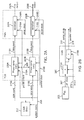
- FIG. 3A shows illustrative bonded transceiver channel circuitry 300 with calibration circuitry in accordance with one embodiment of the present invention.
- Transceiver channels 310A and 310B are coupled together in a bonded configuration in the embodiment of FIG. 3A .
- a transceiver channel may include, among others, clock generation buffer circuitry, a phase detector circuit, and delay circuitry.
- transceiver channel 310A includes its own clock generation buffer circuitry 260A, phase detector circuit 305A, and delay circuitry 306A.
- Clock generation buffer circuitry 260A may generate a parallel clock signal (e.g., parallel_clock 218A) for transceiver channel 310A (and serializer 309A) and clock generation buffer circuitry 260B may generate another parallel clock signal (e.g., parallel_clock 218B) for transceiver channel 310B (and serializer 309B).
- parallel_clock 218A parallel_clock 218A
- clock generation buffer circuitry 260B may generate another parallel clock signal (e.g., parallel_clock 218B) for transceiver channel 310B (and serializer 309B).
- transceiver channel 310A may be a slave transceiver channel and transceiver channel 310B may be a master transceiver channel.
- the parallel clock signal at transceiver channel 318B (e.g., delayed_parallel_clock 308B) may be a master clock signal that is transmitted from the master transceiver channel (e.g., transceiver channel 310B) to the slave transceiver channel (e.g., transceiver channel 310A) to calibrate the slave clock signal at the slave transceiver channel.
- clock generation buffer circuitry 260B may generate a parallel clock signal, parallel_clock signal 218B.
- Delay circuitry 306B may receive parallel_clock signal 218B and is operable to delay parallel_clock signal 218B as needed.
- parallel_clock signal 218B may be transmitted from delay circuitry 306B as delayed_parallel_clock signal 308B without any actual delay applied to the clock signal (e.g., parallel_clock signal 218B).
- delayed_parallel_clock signal 308B may be transmitted from master transceiver channel 310B to phase detector circuit 305A of slave transceiver channel 310A.
- Phase detector circuit 305A compares delayed_parallel_clock signal 308B with delayed_parallel_clock signal 308A to determine the level of adjustment that may be needed for delayed_parallel_clock signal 308A. Phase detector circuit 305A may then generate a control signal (e.g., phase_out signal 302A) to adjust the phase of the slave clock signal (in this case, delayed_parallel_clock signal 308A) based on delayed_parallel_clock signal 308B that is received at slave transceiver channel 310A.
- a control signal e.g., phase_out signal 302A
- phase detector circuit 305A generates and transmits phase_out signal 302A to calibration logic 320A.
- Calibration logic 320A may generate another control signal, clock_slip signal 322A, to adjust the slave clock signal (e.g., to adjust parallel_clock signal 218A).
- clock_slip signal 322A may delay the slave clock signal, which is generated by clock generation buffer circuitry 260A, by at least one clock cycle to adjust the phase of the slave clock signal (e.g., parallel_clock signal 218A).
- the adjustment made (e.g., an adjustment based on phase_out signal 302A from phase detector circuit 305A) to the slave clock signal at slave transceiver channel 310A at this stage may be known as a coarse-grain adjustment.
- the adjusted slave clock signal from clock generation buffer circuitry 260A (e.g., parallel_clock signal 218A) may be further adjusted by delay circuitry 306A.
- calibration logic 320A may output another control signal (e.g., delay_control signal 324A) and delay circuitry 306A may adjust parallel_clock signal 218A, based on the control signal received from calibration logic 320A.
- the adjustment made by delay circuitry 306A may be known as a fine-grain adjustment, and the resulting signal may be referred to as a fine-tuned clock signal.
- a fine-grain adjustment is a more precise adjustment.
- the fine-grain adjustment may allow delay adjustments to be made in relatively smaller increments compared to the coarse-grain adjustment.
- Delay circuitry 306A may then generate an intermediate slave clock signal such as delayed_parallel_clock signal 308A.
- the intermediate slave clock signal may then be adjusted based on a predetermined offset value.
- the predetermined offset value may be obtained during characterization of the device.
- the slave clock signal at slave transceiver channel 310A may thus be aligned with the master clock signal at master transceiver channel 310B after the intermediate slave clock signal has been shifted by the predetermined offset value.
- the aligned slave clock signal (in this case, delayed_parallel_clock signal 308A) may be transmitted from delay circuitry 306A as an output at slave transceiver channel 310A.
- the aligned slave clock signal may be transmitted through bonding control circuitry 225A to a phase compensation FIFO in another transceiver channel to ensure that the phase compensation FIFOs (e.g., phase compensation FIFOs 220A and 220B of FIG. 2A ) are properly synchronized.
- phase compensation FIFOs e.g., phase compensation FIFOs 220A and 220B of FIG. 2A
- transceiver channels 310A and 310B may need to arrive at the respective serializers (e.g., serializers 309A and 309A) at approximately the same time.
- serializer 309A receives parallel_clock signal 218A from clock generation buffer circuitry 260A.
- serializer 309A may receive the adjusted slave clock signal (e.g., parallel_clock signal 218A) from clock generation buffer circuitry 260A, and not the fine-tuned clock signal (e.g., delayed_parallel_clock signal 308A) from delay circuitry 306A.
- the adjusted slave clock signal e.g., parallel_clock signal 218A
- the fine-tuned clock signal e.g., delayed_parallel_clock signal 308A
- serializer 309A may receive either the fine-tuned clock signal (e.g., delayed_parallel_clock signal 218A or 218B) from delay circuitry 306A (or 306B) or the adjusted slave clock signal from clock generation buffer circuitry 260A (or 260B) in this context.
- the fine-tuned clock signal e.g., delayed_parallel_clock signal 218A or 218B
- the adjusted slave clock signal from clock generation buffer circuitry 260A (or 260B) in this context.
- transceiver channel 310B may operate similarly as their respective circuit elements in transceiver channel 310A, and as such, for the sake of brevity, the functionality of these circuit elements are not described in detail again.
- transceiver channel 310B may receive a calibration clock signal 308C from another transceiver channel (not shown in FIG.
- phase detector circuit 305B may compare the phase difference between the clock signal generated by clock generation buffer circuitry 260B (e.g., parallel_clock signal 218B) and clock signal 308C, and output a control signal, phase_out 302B, to calibration logic 320B.
- Calibration logic 320B may generate delay_control signal 324B and clock_slip signal 322B to tune the clock signal at transceiver channel 310B (namely, parallel_clock signal 218B which is generated by clock generation buffer circuitry 260B) according to clock signal 308C that is received from the other transceiver channel.
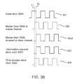
- FIG. 3B shows illustrative waveforms that depict the different stages of slave and master clock signals in accordance with one embodiment of the present invention.
- Waveform 391 may represent the initial phase of slave clock signal 308A at transceiver channel 310A of FIG. 3A and waveform 392 may represent the initial phase of master clock signal 308B at transceiver channel 310B of FIG. 3A .
- the first rising edge of the master clock signal 308B may correspond to time T1.
- Waveform 392B depicts the master clock signal 308B received at a slave transceiver channel. It should be appreciated that there may be some propagation delay when master clock signal 308B is transmitted to the slave transceiver channel (e.g., 310A of FIG. 3A ), and as such, the first rising edge of the master clock signal 308B received at the slave transceiver channel may correspond to time T2 (e.g., at a time later than time T1). Accordingly, the slave clock signal at the slave transceiver channel (e.g., parallel_clock signal 218A at transceiver channel 310A of FIG. 3A ) may be adjusted according to the phase of the received master clock signal 308B. In the embodiment of FIG. 3A , phase detector circuit 305A outputs phase_out signal 302A to calibration logic 320A and in turn to control clock_slip signal 322A in order to adjust the phase of the clock signal generated by clock generation buffer circuitry 260A.
- phase detector circuit 305A outputs phase_
- Waveform 393 represents the intermediate adjusted slave clock signal that is adjusted according to the master clock signal 308B received at the slave transceiver channel. As shown by waveforms 392B and 393, the edges of the intermediate adjusted slave clock signal may align with the edges of the received master clock signal (e.g., the first rising edge of the intermediate adjusted clock signal correspond to the first rising edge of the received master clock signal at time T2).
- the slave clock signal 308A may be further adjusted by a predetermined offset value so that the edges of the adjusted slave clock signal may be aligned with the edges of the master clock signal 308B at the master transceiver channel. As shown in the waveform 394 of FIG. 3B , the first rising edge of the final adjusted slave clock signal 308A (at the slave transceiver channel) is aligned with the first rising edge of the master clock signal 308B (at the master transceiver channel) at time T1.
- FIG. 4 shows illustrative method 400 for calibrating clock signals in an integrated circuit in accordance with one embodiment of the present invention.
- a master clock signal may be routed from a master channel to a slave channel.
- the slave clock signal at the slave channel may be adjusted according to the master clock signal received at the slave channel at step 420.
- the adjusted slave clock signal may be represented by waveform 393 of FIG. 3B .
- the slave clock signal may further be adjusted by a predetermined offset value.
- the predetermined offset value may be obtained during characterization of the integrated circuit and may be stored as an offset value in the integrated circuit.
- the final adjusted slave clock signal may be similar to the adjusted slave clock signal as represented by waveform 394 of FIG. 3B (where edges of the adjusted slave clock signal may be aligned with the edges of the master clock signal at the master channel).
- FIG. 5A shows illustrative transceiver channel circuit 500A with calibration circuitry in accordance with one embodiment of the present invention. It should be appreciated that transceiver channel circuit 500A shares similarities with transceiver channels 310A and 310B of FIG. 3A . As such, for the sake of brevity, signals and elements that have been described above (e.g., clock generation buffer circuitry 260, calibration logic 320, phase detector circuit 305, serializer 309, delay circuitry 306, etc.) will not be described in detail again.
- transceiver channel circuit 500A includes multiple selector circuits, namely, selector circuits 510A-510C.
- Each of the selector circuits 510A-510C may be a two-input multiplexing circuit that may be configured to route different clock signals to or from transceiver channel circuit 500A (the details of which will be shown in FIGS. 6A and 7A ).
- multiplexing circuit 510A may receive an input signal 504 from a top transceiver channel (not shown) and another input signal 502 from a bottom transceiver channel (not shown).
- input signals 504 and 502 may be clock signals from adjacent transceiver channels.
- multiplexing circuit 510A may selectively couple a clock signal (either from a top transceiver channel or a bottom transceiver channel) to phase detector circuit 305.
- phase detector circuit 305 may compare the phase of the selected clock signal (e.g., either input signal 504 or 502) with the clock signal (e.g., delayed_parallel_clock signal 308) at transceiver channel 500A.
- multiplexing circuit 510B may receive the clock signal (e.g., delayed_parallel_clock signal 308) at transceiver channel 500A and clock signal 502 from a different transceiver channel (e.g., a bottom adjacent transceiver channel). Multiplexing circuit 510B may then selectively transmit either one of the clock signals as an output 512 to another transceiver channel (e.g., a top adjacent transceiver channel).
- the clock signal e.g., delayed_parallel_clock signal 308
- multiplexing circuit 510B may then selectively transmit either one of the clock signals as an output 512 to another transceiver channel (e.g., a top adjacent transceiver channel).
- multiplexing circuit 510C may receive the clock signal (e.g., delayed_parallel_clock signal 308) at transceiver channel 500A and another clock signal 504 from a different transceiver channel (e.g., a top adjacent transceiver channel), and selectively transmit either one of the clock signals as an output 514 to another transceiver channel (e.g., a bottom adjacent transceiver channel).
- a different transceiver channel e.g., a top adjacent transceiver channel
- another transceiver channel e.g., a bottom adjacent transceiver channel.
- transceiver channels similar to transceiver channel 500A may be coupled together.
- Each transceiver channel may also include multiplexing circuits such as multiplexing circuits 510A-510C that may be used to route signals or clock signals from one transceiver channel to another.
- FIG. 5B shows illustrative transceiver channel 500B in accordance with another embodiment of the present invention.
- transceiver channel 500B shares similarities with transceiver channel 500A of FIG. 5A and as such, for the sake of brevity, elements (e.g., multiplexing circuits 510A-510C, etc.) that have been described above are not repeated.
- parallel_clock signal 218 generated by clock buffer circuitry 260 may not be transmitted directly to serializer 309.
- serializer 309 receives a delayed clock signal (e.g., delayed_parallel_clock signal 308) from delay circuitry 306). Transmitting the delayed clock signal to the serializer 309 may allow for fine-grain control of serializer 309.
- serializer 309 may include a phase interpolator (not shown) to further adjust the phase of the delayed clock signal.
- FIG. 6A depicts two transceiver channels (e.g., transceiver channel 610A and 610B) coupled together in accordance with one embodiment of the present invention.
- transceiver channels 610A and 610B may be similar to transceiver channel 500A of FIG. 5A .
- transceiver channel 500B of FIG. 5B may also be used in this context (e.g., multiple transceiver channels 500B may be coupled together).
- transceiver channel 610A may be a slave transceiver channel that receives a calibration clock signal from a master transceiver channel (e.g., transceiver channel 610B).
- transceiver channel 610B This may be referred to as “bonding up” as transceiver channel 610B, as shown in FIG. 6A , may be a transceiver channel at the bottom of transceiver channel 610A.
- the dotted line in FIG. 6A shows the "bonding up” path of the clock signal transmitted from transceiver channel 610B to transceiver channel 610A.
- Multiplexing circuits 510A may be configured to select and transmit a clock signal from transceiver channel 610B to transceiver channel 610A. Accordingly, multiplexing circuit 510Y in transceiver channel 610B may be configured to transmit the clock signal at transceiver channel 610B (e.g., delayed_parallel_clock signal 308B) to transceiver channel 610A. It should be appreciated that even though multiplexing circuit 510Y is shown transmitting the clock signal, delayed_parallel_clock signal 308B, from transceiver channel 610B, multiplexing circuit 510Y may be configured such that another clock signal 502B from another transceiver channel may be transmitted as calibration clock signal to transceiver channel 610A instead.
- the slave clock signal (e.g., delayed_parallel_clock signal 308A) at transceiver channel 610A may be adjusted or calibrated based on the master clock signal (e.g., delayed_parallel_clock signal 308B) from transceiver channel 610B.
- Phase detector circuit 305A may compare the phase of the slave clock signal at transceiver channel 610A with the phase of the received master clock signal 308B.
- phase detector circuit 305A may output phase_out signal 302A to calibration logic 320A such that calibration logic 320A may generate a control signal (e.g., clock_slip 322A) to delay or adjust the clock signal (parallel_clock 218A) generated by clock generation buffer circuitry 260A. The clock signal may then be further adjusted by delay circuitry 306A.
- a control signal e.g., clock_slip 322A
- the clock signal may then be further adjusted by delay circuitry 306A.
- FIG. 6B shows illustrative waveforms that depict the slave and master clock signals of two transceiver channels that are coupled together in accordance with one embodiment of the present invention.
- the waveforms depict when master clock signal 308B arrives at the slave transceiver channel, (e.g., transceiver channel 610A) and how slave clock signal 308A is adjusted according to the received master clock signal 308B.
- Waveform 650A shows slave clock signal 308A at the slave transceiver channel (e.g., transceiver channel 610A) prior to any adjustment
- waveform 660A shows master clock signal 308B at the master transceiver channel (e.g., transceiver channel 610B).
- Waveform 660B shows master clock signal 308B received at the slave transceiver channel (e.g., slave transceiver channel 610A) with propagation delay.
- master clock signal 308B received at the slave transceiver channel may be slightly delayed compared to the master clock signal 308B at the master transceiver channel.
- slave clock signal 308A may then be adjusted based on the received master clock signal 308B.
- Waveform 650B shows the resulting intermediate adjusted slave clock signal 308A at the slave transceiver channel.
- Slave clock signal 308A may be adjusted such that its edges are aligned with the edges of the master clock signal 308B that is received at the slave transceiver channel.
- the first rising edges of the respective master and slave clock signals are aligned at time T2 (as shown by waveforms 660B and 650B). It should be appreciated that such an adjustment may be made in response to the comparison made between the two clock signals (master and slave clock signals, 308B and 308A) by phase detector circuit 305A of FIG. 6A .
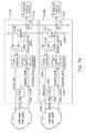
- FIG. 7A shows illustrative transceiver channels 610A and 610B in a "bonding down" configuration and a resulting adjusted slave clock output with propagation delay compensation in accordance with one embodiment of the present invention.
- transceiver channel 610A may be a slave transceiver channel and transceiver channel 610B may be a master transceiver channel.
- the dotted line in FIG. 7A shows the "bonding down" path of the clock signal transmitted from transceiver channel 610A to transceiver channel 610B.
- the slave clock signal (e.g., delayed_parallel_clock signal 308A) is routed from transceiver channel 610A to transceiver channel 610B through multiplexing circuit 510C.
- multiplexing circuit 510X at transceiver channel 610B may be configured to route the slave clock signal 308A from transceiver channel 610A as an input to phase detector circuit 305B.
- the master clock signal at transceiver channel 610B may then be adjusted according to the received slave clock signal.
- phase detector circuit 305B may compare the phase of the master clock signal 308B at transceiver channel 610B with the phase of the received slave clock signal 308A. Phase detector circuit 305B may then output phase_out signal 302B to calibration logic 320B so that calibration logic 320B may generate a control signal (e.g., clock_slip 322B) to delay or adjust the master clock signal (e.g., parallel_clock 218B) generated by clock generation buffer circuitry 260B. In one embodiment, the master clock signal is adjusted such that edges of the master clock signal align with edges of the slave clock signal 308A that is received at master transceiver channel 610B.
- a control signal e.g., clock_slip 322B
- the master clock signal is adjusted such that edges of the master clock signal align with edges of the slave clock signal 308A that is received at master transceiver channel 610B.
- the slave clock signal at slave transceiver channel 610A may further be adjusted so that it is fully aligned with the master clock signal at master transceiver channel 610B (the details of which will be explained by method 800 of FIG. 8 ).
- the slave clock signal at slave transceiver channel 610A may also be adjusted based on a predetermined offset value obtained during characterization of the integrated circuit.
- multiplexing circuit 510B be configured to route a clock signal from either transceiver channel 610A or 610B to another transceiver channel (not shown) above transceiver channel 610A.
- multiplexing circuit 510Z at transceiver channel 610B may be configured to route a clock signal from either transceiver channel 610A or 610B to yet another transceiver channel (not shown) below transceiver channel 610B.
- multiplexing circuit 570Y may be configured such that a clock signal 502B from another transceiver channel (not shown) is transmitted to transceiver channel 610A instead.
- clock signals from one transceiver channel may be routed to any other transceiver channel in the integrated circuit.
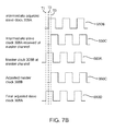
- FIG. 7B shows illustrative waveforms that depict the slave and master clock signals of two transceiver channels in a "bonding down" configuration in accordance with one embodiment of the present invention.
- Waveform 650B shows the intermediate adjusted slave clock signal 308A with a first rising edge at time T2 after the adjustment made with the "bonding up" of transceiver channel 610B (as shown in the embodiment of FIG. 6A ).
- the intermediate adjusted slave clock signal 308A is routed to the master transceiver channel (as shown in the "bonding down" configuration in FIG. 7A ).
- Waveform 650C depicts the intermediate adjusted slave clock signal 308A as received by the master transceiver channel (e.g., transceiver channel 610B of FIG. 7A ). It should be appreciated that there may be propagation delay as the intermediate adjusted slave clock signal 308A is routed to the master transceiver channel. As such, the first rising edge of the intermediate adjusted slave clock signal 308A, received at the master transceiver channel, occurs at a slightly later time (e.g., time T3) compared to the same clock signal 308A at the slave transceiver channel (as shown by waveform 650B).
- time T3 a slightly later time
- Waveform 660A depicts master clock signal 308B at the master transceiver channel prior to any adjustment.
- the master clock signal 308B at the master transceiver channel may be adjusted accordingly.
- Waveform 660C shows the result of the adjusted master clock signal 308B.
- the master clock 308B at the master transceiver is adjusted so that its edges are aligned with the edges of the intermediate slave clock signal 308A that is received at the master transceiver channel. As shown in FIG.
- the first rising edges of the respective master and slave clock signals are aligned at time T3 (as shown by waveforms 650C and 660C).
- the total adjustment made to the master clock signal at the master transceiver channel e.g., shifting the first rising edge of the master clock signal from time T1 to time T3 may then be used to further adjust the slave clock signal 308A at the slave transceiver channel.
- the total adjustment made to the master clock signal at this stage is known as a total propagation delay for a "round-trip" made by the master clock signal 308B by routing the master clock signal 308B to the slave transceiver channel and back to the master transceiver channel.
- the intermediate adjusted slave clock signal 308A may be shifted back (e.g., shifted to the left) based on half the total adjustment made to the master clock signal 308B (assuming the propagation delays between the master and slave transceiver channels are symmetrical) to fully align the slave clock signal 308A with the master clock signal 308B.
- the propagation delays from the master transceiver channel to the slave transceiver channel and back may not be symmetrical.
- the intermediate adjusted slave clock signal 308A may further be adjusted based on a predetermined offset value (or relevant characterization information stored on the integrated circuit).
- Waveform 650D depicts the final adjusted slave clock signal 308A at the slave transceiver channel.
- the first rising edge of the intermediate adjusted slave clock signal 308A may be at time T2 (as shown by waveform 650B).
- the total adjustment made to the master clock signal 308B at the master transceiver channel based on the intermediate adjusted slave clock signal 308A that is received at the master transceiver channel is T3-T1 (as shown by waveforms 660A and 660C).
- the final adjustment needed to be made to the intermediate adjusted slave clock signal 308A at the slave transceiver channel may be obtained by dividing the total adjustment made to the master clock signal 308B by half (e.g., half of the difference between T3 and T1). It should be appreciated that after the total adjustment required is obtained, the master clock signal 308B at the master transceiver channel may be returned to its pre-adjustment state.
- the final adjusted slave clock signal 308A at the slave transceiver channel may be fully aligned with the master clock signal 308B at the master transceiver channel (prior to any adjustment, as represented by waveform 660A).
- the slave and master clock signals at their respective slave and master transceiver channels may thus be fully aligned after the "bonding-up” and “bonding-down" of both transceiver channels (e.g., transceiver channels 610A and 610B as shown in FIGS. 6A and 7A ).
- FIG. 8 shows illustrative method 800 for aligning clock signals in an integrated circuit in accordance with one embodiment of the present invention.
- a master clock signal is routed from a master channel to a slave channel.
- a slave clock signal at the slave channel may be adjusted according to the master clock signal.
- the master clock signal from transceiver channel 610B is routed to transceiver channel 610A and the slave clock signal at transceiver channel 610A is then adjusted according to the received master clock signal.
- the slave clock signal is then routed from the slave channel to the master channel.
- the master clock signal at the master channel is then adjusted according to the received slave clock signal.
- the dotted line in the embodiment of FIG. 7A shows the routing of the slave clock signal to the master transceiver channel 610B.
- the slave clock signal at this stage may have been adjusted at the slave transceiver channel according to the master clock signal that is routed to the slave transceiver channel.
- the master clock signal at the master channel at this stage may be adjusted according to the intermediate adjusted slave clock signal that is received at the master transceiver channel (as represented by waveform 650C of FIG. 7B ).
- the total adjustment made to the master clock signal at this stage may be recorded before the master clock signal is returned to its pre-adjustment state at step 850.
- waveform 660A shows the master clock signal at its pre-adjustment state.
- the slave clock signal at the slave channel is then adjusted based on the prior adjustment (recorded at step 840) made to the master clock signal at the master transceiver channel.
- the slave clock signal is shifted back by half the total adjustment made to the master clock signal such that the slave clock signal at the slave transceiver channel may be aligned with the master clock signal at the master transceiver channel.
- Waveforms 650A and 650D of FIG. 7B may represent, respectively, the master clock signal at the master transceiver channel, and the final adjusted slave clock signal at the slave transceiver channel.
- CMOS complementary metal-oxide-semiconductor
- PAL programmable array logic
- PLA programmable logic arrays
- FPLA field programmable logic arrays
- EPLD electrically programmable logic devices
- EEPLD electrically erasable programmable logic devices
- LCDA logic cell arrays
- FPGA field programmable gate arrays
- ASSP application specific standard products
- ASIC application specific integrated circuits
- the programmable logic device described herein may be part of a data processing system that includes one or more of the following components; a processor; memory; I/O circuitry; and peripheral devices.
- the data processing system can be used in a wide variety of applications, such as computer networking, data networking, instrumentation, video processing, digital signal processing, or any suitable other application where the advantage of using programmable or re-programmable logic is desirable.
- the programmable logic device can be used to perform a variety of different logic functions.
- the programmable logic device can be configured as a processor or controller that works in cooperation with a system processor.
- the programmable logic device may also be used as an arbiter for arbitrating access to a shared resource in the data processing system.
- the programmable logic device can be configured as an interface between a processor and one of the other components in the system.
- the programmable logic device may be one of a family of devices owned by the assignee.
Landscapes
- Engineering & Computer Science (AREA)
- Theoretical Computer Science (AREA)
- Physics & Mathematics (AREA)
- General Engineering & Computer Science (AREA)
- General Physics & Mathematics (AREA)
- Synchronisation In Digital Transmission Systems (AREA)
- Computer Networks & Wireless Communication (AREA)
- Signal Processing (AREA)
Abstract
Description
- Integrated circuit devices, such as field-programmable gate arrays (FPGAs), application specific integrated circuits (ASICs), and the like, may be used to implement a variety of functions. For instance, an FPGA device may be configured to perform various user functions based on different user designs. Integrated circuit devices may be employed in various different systems (e.g., communication systems).
- An integrated circuit device may include multiple input-output elements that support a wide variety of protocols. As an example, an integrated circuit device may include high-speed transceiver (transmitter and receiver) channels that may be used to communicate with other components or circuits connected to the device. Transceiver channels on an integrated circuit device typically support multiple different input-output protocols.
- Many multi-lane high-speed serial interface protocols (e.g., Interlaken, PCI Express, XAUI) may impose a requirement on the amount of data skew that can exist between any two transmit channels in a particular interface. To ensure proper synchronization between the different channels, circuitry may be used to minimize skew. Such circuitry may be used to "bond" transceiver channels (e.g., to reduce skew between each pair of transceiver channels).
- Generally, conventional techniques for transceiver channel bonding impose several limitations and tradeoffs (e.g., limits on supported data rates, the number of channels that can be bonded, the placement of channels, etc.). To overcome some of these limitations and tradeoffs, integrated circuit devices typically include circuitry to support multiple different bonding methods. The need to include such types of bonding circuitry, however, results in additional silicon area overhead and may increase design complexity (i.e., longer verification time is needed).
- Circuitry and techniques for dynamically minimizing skew across multiple input-output elements (e.g., transceiver channels) in a high-speed serial interface are provided. Embodiments of the present invention include circuits and techniques to bond multiple transceiver channels together.
- It is appreciated that the present invention can be implemented in numerous ways, such as a process, an apparatus, a system, or a device. Several inventive embodiments of the present invention are described below.
- A method of aligning clock signals in multiple transceiver channels in an integrated circuit may include adjusting a phase of a slave clock signal based on a phase of a master clock signal to produce an intermediate slave clock signal. The master clock channel may be received from a master transceiver channel. The phase of the master clock signal may then be adjusted based on the phase of the intermediate slave clock signal produced by a slave transceiver channel. A total adjustment value is obtained based on the adjustment made and the phase of the intermediate slave clock signal may be further adjusted at the slave transceiver channel based on the total adjustment value obtained. An adjusted slave clock signal may be produced by the slave transceiver channel.
- A method of calibrating clock signals in an integrated circuit may include receiving clock signals at different transceiver channel circuitries and adjusting the received clock signals. As an example, first transceiver channel circuitry with a first clock signal may receive a second clock signal from second transceiver channel circuitry. The first transceiver channel circuitry may include clock generation circuitry. The clock generation circuitry may adjust the phase of the first clock signal based on the phase of the second clock signal received at the first transceiver channel circuitry. In one embodiment, the first transceiver channel circuitry may further include delay circuitry. The phase of the first clock signal may be adjusted with the delay circuitry based on a predetermined offset value to align the phase of the second clock signal at the second transceiver channel circuitry.
- An integrated circuit may include transceiver channel circuitry with clock circuitry operable to output a channel clock signal. The integrated circuit may further include a phase detector circuit that is operable to compare the channel clock signal with a reference clock signal to produce a phase output signal in response to the comparison between the channel clock signal and the reference clock signal. The integrated circuit may also include delay circuitry operable to receive the channel clock signal and the phase output signal to produce a delayed channel clock signal based on the channel clock signal and the control signal.
-
-
FIG. 1 is a block diagram of an illustrative integrated circuit in accordance with one embodiment of the present invention. -
FIG. 2A shows two illustrative serializers coupled in a bonded configuration in accordance with one embodiment of the present invention. -
FIG. 2B shows illustrative clock generation buffer circuitry in accordance with one embodiment of the present invention. -
FIG. 3A shows illustrative bonded transceiver channel circuitry with calibration circuitry in accordance with one embodiment of the present invention. -
FIG. 3B shows illustrative waveforms that depict the different stages of slave and master clock signals in accordance with one embodiment of the present invention. -
FIG. 4 shows illustrative steps for calibrating clock signals in an integrated circuit in accordance with one embodiment of the present invention. -
FIG. 5A shows an illustrative transceiver channel circuit with calibration circuitry in accordance with one embodiment of the present invention. -
FIG. 5B shows an illustrative transceiver channel in accordance with another embodiment of the present invention. -
FIG. 6A depicts two illustrative transceiver channels together in a "bonding up" configuration in accordance with one embodiment of the present invention. -
FIG. 6B shows illustrative waveforms that depict the slave and master clock signals of two transceiver channels in the "bonding up" configuration in accordance with one embodiment of the present invention. -
FIG. 7A shows illustrative transceiver channels in a "bonding down" configuration in accordance with one embodiment of the present invention. -
FIG. 7B shows illustrative waveforms that depict the slave and master clock signals of two transceiver channels in the "bonding down" configuration and a resulting adjusted slave clock output with propagation delay compensation applied in accordance with one embodiment of the present invention. -
FIG. 8 is a flow chart of illustrative steps for aligning clock signals in an integrated circuit in accordance with one embodiment of the present invention. - The embodiments provided herein include circuitry and techniques to synchronize clock signals (e.g., clock signals between different input-output channels) in an integrated circuit (IC).
- It will be obvious to one skilled in the art that the present exemplary embodiments may be practiced without some or all of these specific details. In other instances, well-known operations have not been described in detail in order not to unnecessarily obscure the present embodiments.
- An IC device such as a field-programmable gate array (FPGA) device, generally includes high-speed input-output circuitry, including, among others, transceiver channels.
FIG. 1 , meant to be illustrative and not limiting, shows a simplified block diagram ofIC 100 that can implement embodiments of the present invention. Generally, an IC device such as IC 100 includescore logic region 115 and input-output elements 110. Other auxiliary circuits, such as phase-locked loops (PLLs) 125 for clock generation and timing, can be located outside the core logic region 115 (e.g., at corners ofIC 100 and adjacent to input-output elements 110) or elsewhere onIC 100. -
Core logic region 115 may be populated with logic cells that include "logic elements" (LEs) 117, among other circuits.LEs 117 may include look-up table-based logic regions and may be grouped into "Logic Array Blocks" (LABs).LEs 117 and groups of LEs or LABs can be configured to perform logical functions desired by the user. Configuration data loaded into configuration memory can be used to produce control signals that configureLEs 117 and groups of LEs and LABs to perform the desired logical functions. Signals received from external circuitry at input-output elements 110 may be routed from input-output elements 110 tocore logic region 115 and other logic blocks onIC 100.Core logic region 115 and other logic blocks onIC 100 may perform functions based on the signals received. - Signals may be sent from
core logic region 115 and other relevant logic blocks ofIC 100 to other external circuitry or components that may be connected toIC 100 through input-output elements 110. A single device likeIC 100 can potentially support a variety of different interfaces and each individual input-output bank 110 can support a different input-output standard with a different interface or protocol (e.g., a high-speed serial interface protocol). - In the embodiment of
FIG. 1 , input-output elements 110 may include input-output buffers and high-speed transmitter/receiver circuitry that connectIC 100 to other external components. A transceiver channel may generally be divided into two blocks (not shown inFIG. 1 ). A transceiver channel may, for example, include a physical coding sublayer (PCS) block and a physical medium attachment (PMA) block. The PCS block is a block that is located between the core region of the device (e.g., core region 115) and the PMA block. The PCS may include, among others, decoders, encoders, alignment circuitry, and registers such as first-in-first-out (FIFO) blocks. The PMA block generally connects the IC device (e.g., IC 100) to the channel, generates the required clocks, and converts data from parallel to serial (and from serial to parallel). - Accordingly, in a transceiver channel, a serializer may be included in the PMA transmitter block. The serializer may take in a parallel data word and serialize the data for transmission at a higher serial data rate. As an example, a parallel data word may be latched into the serializer by a parallel clock and shifted out of the serializer by a serial clock (e.g., a clock signal that typically exhibits a higher frequency compared to the parallel clock).
- Multiple transceiver channels, or more specifically, serializers in the different transceiver channels may be coupled together in a bonded configuration.
FIG. 2A shows two serializers, 250A and 250B, paired together in a bonded configuration in accordance with one embodiment of the present invention. It should be appreciated that even though only two serializers are shown, more serializers may be bonded together in this context. In the embodiment ofFIG. 2A , serializers 250A and 250B receivedata words logic block 210 viaphase compensation FIFOs Logic block 210 may be a protocol interface logic block that is implemented in the core region of an integrated circuit (e.g.,core region 115 ofFIG. 1 ).Phase compensation FIFOs - In the embodiment of
FIG. 2A , serializers 250A and 250B may be part of the PMA block. As mentioned above,serializers FIG. 2A ,phase compensation FIFOs system clock signal 208 and the respective parallel clock signals, 218A and 218B. It should be appreciated that each transceiver channel may include a dedicated phase compensation FIFO (e.g.,phase compensation FIFOs -
Data words data words respective serializers circuitry bus 225 inFIG. 2A ) may be used to ensure that the read side of the phase compensation FIFOs (e.g., 220A and 220B) for every transceiver channel is released simultaneously so thatdata words phase compensation FIFOs - In one embodiment, the bonding control circuitry (shown as
bonding circuitry bus 225 coupled betweenphase compensation FIFOs phase compensation FIFOs FIFOs phase compensation FIFOs data words respective serializers - It should be appreciated that
serializers parallel data words outputs FIG. 2A , serializers 250A and 250B are clocked by respective parallel clock signals 218A and 218B and respective serial clock signals 248A and 248B. It should be appreciated that each transceiver channel may include its own clock generation circuitry (not shown inFIG. 2A ) to generate its own serial and parallel clock signals. - Accordingly, the parallel clock signals (e.g., 218A and 218B) and serial clock signals (248A and 248B) may be generated by their respective clock generation buffer circuits (the details of which will be explained in reference to
FIG 2B below). Skew (or more specifically, serial clock skew) may arise betweenserializers parallel data words serializers phase compensation FIFOs -
FIG. 2B shows illustrative clockgeneration buffer circuitry 260 in accordance with one embodiment of the present invention. Clockgeneration buffer circuitry 260 may receive a high frequency clock from a clock source, such aspll_clock 267 fromPLL circuitry 265, and a reset signal, (e.g., reset 270). Clockgeneration buffer circuitry 260 may also include multiple divider circuits such asdivider circuits 275A and 275B. - Divider circuit 275A divides the input clock signal (in this case, pll_clock 267) to produce a high-frequency serial clock signal (e.g., serial_clock 248), and
divider circuit 275B further divides the input clock signal to produce a low-frequency parallel clock (e.g., parallel_clock 218). It should be appreciated that each transceiver channel may have its own clock generation buffer circuitry such as clockgeneration buffer circuitry 260 to allow each channel to run separately in non-bonded configurations. However, in bonded configurations, clock skew may occur between clocks across multiple channels when each channel produces its own divided clocks. Thus, calibration may be needed to minimize skew between multiple bonded transceiver channels (e.g., calibration to reduce data skew betweenphase compensation FIFOs FIG. 2A ). -
FIG. 3A shows illustrative bondedtransceiver channel circuitry 300 with calibration circuitry in accordance with one embodiment of the present invention.Transceiver channels FIG. 3A . A transceiver channel may include, among others, clock generation buffer circuitry, a phase detector circuit, and delay circuitry. As an example,transceiver channel 310A includes its own clockgeneration buffer circuitry 260A,phase detector circuit 305A, and delaycircuitry 306A. Clockgeneration buffer circuitry 260A may generate a parallel clock signal (e.g.,parallel_clock 218A) fortransceiver channel 310A (andserializer 309A) and clockgeneration buffer circuitry 260B may generate another parallel clock signal (e.g.,parallel_clock 218B) fortransceiver channel 310B (andserializer 309B). - In bonded
transceiver channel circuitry 300,transceiver channel 310A may be a slave transceiver channel andtransceiver channel 310B may be a master transceiver channel. As such, the parallel clock signal at transceiver channel 318B (e.g.,delayed_parallel_clock 308B) may be a master clock signal that is transmitted from the master transceiver channel (e.g.,transceiver channel 310B) to the slave transceiver channel (e.g.,transceiver channel 310A) to calibrate the slave clock signal at the slave transceiver channel. - As an example, clock
generation buffer circuitry 260B may generate a parallel clock signal, parallel_clock signal 218B.Delay circuitry 306B may receiveparallel_clock signal 218B and is operable to delayparallel_clock signal 218B as needed. For instance, prior to calibration, parallel_clock signal 218B may be transmitted fromdelay circuitry 306B asdelayed_parallel_clock signal 308B without any actual delay applied to the clock signal (e.g., parallel_clock signal 218B). In the embodiment ofFIG. 3A , delayed_parallel_clock signal 308B may be transmitted frommaster transceiver channel 310B to phasedetector circuit 305A ofslave transceiver channel 310A.Phase detector circuit 305A comparesdelayed_parallel_clock signal 308B withdelayed_parallel_clock signal 308A to determine the level of adjustment that may be needed fordelayed_parallel_clock signal 308A.Phase detector circuit 305A may then generate a control signal (e.g.,phase_out signal 302A) to adjust the phase of the slave clock signal (in this case,delayed_parallel_clock signal 308A) based ondelayed_parallel_clock signal 308B that is received atslave transceiver channel 310A. - In the embodiment of
FIG. 3A ,phase detector circuit 305A generates and transmitsphase_out signal 302A tocalibration logic 320A.Calibration logic 320A may generate another control signal,clock_slip signal 322A, to adjust the slave clock signal (e.g., to adjustparallel_clock signal 218A). In one embodiment,clock_slip signal 322A may delay the slave clock signal, which is generated by clockgeneration buffer circuitry 260A, by at least one clock cycle to adjust the phase of the slave clock signal (e.g.,parallel_clock signal 218A). - In one embodiment, the adjustment made (e.g., an adjustment based on
phase_out signal 302A fromphase detector circuit 305A) to the slave clock signal atslave transceiver channel 310A at this stage may be known as a coarse-grain adjustment. The adjusted slave clock signal from clockgeneration buffer circuitry 260A (e.g.,parallel_clock signal 218A) may be further adjusted bydelay circuitry 306A. In one embodiment,calibration logic 320A may output another control signal (e.g.,delay_control signal 324A) anddelay circuitry 306A may adjustparallel_clock signal 218A, based on the control signal received fromcalibration logic 320A. The adjustment made bydelay circuitry 306A may be known as a fine-grain adjustment, and the resulting signal may be referred to as a fine-tuned clock signal. Compared to a coarse-grain adjustment, a fine-grain adjustment is a more precise adjustment. For instance, the fine-grain adjustment may allow delay adjustments to be made in relatively smaller increments compared to the coarse-grain adjustment. -
Delay circuitry 306A may then generate an intermediate slave clock signal such asdelayed_parallel_clock signal 308A. In one embodiment, the intermediate slave clock signal may then be adjusted based on a predetermined offset value. As an example, the predetermined offset value may be obtained during characterization of the device. The slave clock signal atslave transceiver channel 310A may thus be aligned with the master clock signal atmaster transceiver channel 310B after the intermediate slave clock signal has been shifted by the predetermined offset value. - The aligned slave clock signal (in this case,
delayed_parallel_clock signal 308A) may be transmitted fromdelay circuitry 306A as an output atslave transceiver channel 310A. In one embodiment, the aligned slave clock signal may be transmitted throughbonding control circuitry 225A to a phase compensation FIFO in another transceiver channel to ensure that the phase compensation FIFOs (e.g.,phase compensation FIFOs FIG. 2A ) are properly synchronized. It should be appreciated that in order to reduce skew between bonded channels, parallel data from the phase compensation FIFOs (not shown in the embodiment ofFIG. 3A ) at the respective transceiver channels (e.g.,transceiver channels - As shown in
FIG. 3A , serializer 309A receivesparallel_clock signal 218A from clockgeneration buffer circuitry 260A. As such,serializer 309A may receive the adjusted slave clock signal (e.g.,parallel_clock signal 218A) from clockgeneration buffer circuitry 260A, and not the fine-tuned clock signal (e.g.,delayed_parallel_clock signal 308A) fromdelay circuitry 306A. However, it should be appreciated thatserializer 309A (or 309B) may receive either the fine-tuned clock signal (e.g.,delayed_parallel_clock signal delay circuitry 306A (or 306B) or the adjusted slave clock signal from clockgeneration buffer circuitry 260A (or 260B) in this context. - It should be appreciated that circuit elements (e.g., clock generation buffer circuitry 206B,
phase detector circuit 305B, delay circuitry 206B,serializer 309B,bonding control circuitry 225B,calibration logic 320B, etc.) intransceiver channel 310B may operate similarly as their respective circuit elements intransceiver channel 310A, and as such, for the sake of brevity, the functionality of these circuit elements are not described in detail again. For instance,transceiver channel 310B may receive acalibration clock signal 308C from another transceiver channel (not shown inFIG. 3A ) andphase detector circuit 305B may compare the phase difference between the clock signal generated by clockgeneration buffer circuitry 260B (e.g., parallel_clock signal 218B) andclock signal 308C, and output a control signal,phase_out 302B, tocalibration logic 320B.Calibration logic 320B, in turn, may generate delay_control signal 324B and clock_slip signal 322B to tune the clock signal attransceiver channel 310B (namely, parallel_clock signal 218B which is generated by clockgeneration buffer circuitry 260B) according toclock signal 308C that is received from the other transceiver channel. -
FIG. 3B shows illustrative waveforms that depict the different stages of slave and master clock signals in accordance with one embodiment of the present invention.Waveform 391 may represent the initial phase ofslave clock signal 308A attransceiver channel 310A ofFIG. 3A andwaveform 392 may represent the initial phase ofmaster clock signal 308B attransceiver channel 310B ofFIG. 3A . As shown in the embodiment ofFIG. 3B , the first rising edge of themaster clock signal 308B may correspond to time T1. -
Waveform 392B depicts themaster clock signal 308B received at a slave transceiver channel. It should be appreciated that there may be some propagation delay whenmaster clock signal 308B is transmitted to the slave transceiver channel (e.g., 310A ofFIG. 3A ), and as such, the first rising edge of themaster clock signal 308B received at the slave transceiver channel may correspond to time T2 (e.g., at a time later than time T1). Accordingly, the slave clock signal at the slave transceiver channel (e.g.,parallel_clock signal 218A attransceiver channel 310A ofFIG. 3A ) may be adjusted according to the phase of the receivedmaster clock signal 308B. In the embodiment ofFIG. 3A ,phase detector circuit 305A outputs phase_out signal 302A tocalibration logic 320A and in turn to controlclock_slip signal 322A in order to adjust the phase of the clock signal generated by clockgeneration buffer circuitry 260A. -
Waveform 393 represents the intermediate adjusted slave clock signal that is adjusted according to themaster clock signal 308B received at the slave transceiver channel. As shown bywaveforms - The
slave clock signal 308A may be further adjusted by a predetermined offset value so that the edges of the adjusted slave clock signal may be aligned with the edges of themaster clock signal 308B at the master transceiver channel. As shown in thewaveform 394 ofFIG. 3B , the first rising edge of the final adjustedslave clock signal 308A (at the slave transceiver channel) is aligned with the first rising edge of themaster clock signal 308B (at the master transceiver channel) at time T1. -
FIG. 4 showsillustrative method 400 for calibrating clock signals in an integrated circuit in accordance with one embodiment of the present invention. Atstep 410, a master clock signal may be routed from a master channel to a slave channel. The slave clock signal at the slave channel may be adjusted according to the master clock signal received at the slave channel atstep 420. In one embodiment, the adjusted slave clock signal may be represented bywaveform 393 ofFIG. 3B . Atstep 430, the slave clock signal may further be adjusted by a predetermined offset value. As an example, the predetermined offset value may be obtained during characterization of the integrated circuit and may be stored as an offset value in the integrated circuit. The final adjusted slave clock signal may be similar to the adjusted slave clock signal as represented bywaveform 394 ofFIG. 3B (where edges of the adjusted slave clock signal may be aligned with the edges of the master clock signal at the master channel). -
FIG. 5A shows illustrativetransceiver channel circuit 500A with calibration circuitry in accordance with one embodiment of the present invention. It should be appreciated thattransceiver channel circuit 500A shares similarities withtransceiver channels FIG. 3A . As such, for the sake of brevity, signals and elements that have been described above (e.g., clockgeneration buffer circuitry 260,calibration logic 320,phase detector circuit 305,serializer 309,delay circuitry 306, etc.) will not be described in detail again. - In the embodiment of
FIG. 5A ,transceiver channel circuit 500A includes multiple selector circuits, namely,selector circuits 510A-510C. Each of theselector circuits 510A-510C may be a two-input multiplexing circuit that may be configured to route different clock signals to or fromtransceiver channel circuit 500A (the details of which will be shown inFIGS. 6A and7A ). For instance, as shown inFIG. 5A , multiplexingcircuit 510A may receive aninput signal 504 from a top transceiver channel (not shown) and anotherinput signal 502 from a bottom transceiver channel (not shown). - In one embodiment, input signals 504 and 502 may be clock signals from adjacent transceiver channels. As such,
multiplexing circuit 510A may selectively couple a clock signal (either from a top transceiver channel or a bottom transceiver channel) tophase detector circuit 305. Accordingly, as explained above,phase detector circuit 305 may compare the phase of the selected clock signal (e.g., eitherinput signal 504 or 502) with the clock signal (e.g., delayed_parallel_clock signal 308) attransceiver channel 500A. - In the embodiment of
FIG. 5A , multiplexingcircuit 510B may receive the clock signal (e.g., delayed_parallel_clock signal 308) attransceiver channel 500A and clock signal 502 from a different transceiver channel (e.g., a bottom adjacent transceiver channel). Multiplexingcircuit 510B may then selectively transmit either one of the clock signals as anoutput 512 to another transceiver channel (e.g., a top adjacent transceiver channel). Similarly, multiplexingcircuit 510C may receive the clock signal (e.g., delayed_parallel_clock signal 308) attransceiver channel 500A and anotherclock signal 504 from a different transceiver channel (e.g., a top adjacent transceiver channel), and selectively transmit either one of the clock signals as anoutput 514 to another transceiver channel (e.g., a bottom adjacent transceiver channel). It should be appreciated that multiple transceiver channels similar totransceiver channel 500A may be coupled together. Each transceiver channel may also include multiplexing circuits such asmultiplexing circuits 510A-510C that may be used to route signals or clock signals from one transceiver channel to another. -
FIG. 5B showsillustrative transceiver channel 500B in accordance with another embodiment of the present invention. It should be appreciated thattransceiver channel 500B shares similarities withtransceiver channel 500A ofFIG. 5A and as such, for the sake of brevity, elements (e.g., multiplexingcircuits 510A-510C, etc.) that have been described above are not repeated. In the embodiment ofFIG. 5B ,parallel_clock signal 218 generated byclock buffer circuitry 260 may not be transmitted directly toserializer 309. Instead,serializer 309 receives a delayed clock signal (e.g., delayed_parallel_clock signal 308) from delay circuitry 306). Transmitting the delayed clock signal to theserializer 309 may allow for fine-grain control ofserializer 309. In one embodiment,serializer 309 may include a phase interpolator (not shown) to further adjust the phase of the delayed clock signal. -
FIG. 6A depicts two transceiver channels (e.g.,transceiver channel transceiver channels transceiver channel 500A ofFIG. 5A . However, even though not shown inFIG. 6A , it should also be appreciated thattransceiver channel 500B ofFIG. 5B may also be used in this context (e.g.,multiple transceiver channels 500B may be coupled together). In one embodiment,transceiver channel 610A may be a slave transceiver channel that receives a calibration clock signal from a master transceiver channel (e.g.,transceiver channel 610B). This may be referred to as "bonding up" astransceiver channel 610B, as shown inFIG. 6A , may be a transceiver channel at the bottom oftransceiver channel 610A. The dotted line inFIG. 6A shows the "bonding up" path of the clock signal transmitted fromtransceiver channel 610B totransceiver channel 610A. - Multiplexing
circuits 510A may be configured to select and transmit a clock signal fromtransceiver channel 610B totransceiver channel 610A. Accordingly, multiplexingcircuit 510Y intransceiver channel 610B may be configured to transmit the clock signal attransceiver channel 610B (e.g., delayed_parallel_clock signal 308B) totransceiver channel 610A. It should be appreciated that even though multiplexingcircuit 510Y is shown transmitting the clock signal,delayed_parallel_clock signal 308B, fromtransceiver channel 610B, multiplexingcircuit 510Y may be configured such that anotherclock signal 502B from another transceiver channel may be transmitted as calibration clock signal totransceiver channel 610A instead. - In the embodiment of
FIG. 6A , the slave clock signal (e.g.,delayed_parallel_clock signal 308A) attransceiver channel 610A may be adjusted or calibrated based on the master clock signal (e.g., delayed_parallel_clock signal 308B) fromtransceiver channel 610B.Phase detector circuit 305A may compare the phase of the slave clock signal attransceiver channel 610A with the phase of the receivedmaster clock signal 308B. As explained above,phase detector circuit 305A mayoutput phase_out signal 302A tocalibration logic 320A such thatcalibration logic 320A may generate a control signal (e.g.,clock_slip 322A) to delay or adjust the clock signal (parallel_clock 218A) generated by clockgeneration buffer circuitry 260A. The clock signal may then be further adjusted bydelay circuitry 306A. -
FIG. 6B shows illustrative waveforms that depict the slave and master clock signals of two transceiver channels that are coupled together in accordance with one embodiment of the present invention. The waveforms depict whenmaster clock signal 308B arrives at the slave transceiver channel, (e.g.,transceiver channel 610A) and howslave clock signal 308A is adjusted according to the receivedmaster clock signal 308B.Waveform 650A showsslave clock signal 308A at the slave transceiver channel (e.g.,transceiver channel 610A) prior to any adjustment, andwaveform 660A showsmaster clock signal 308B at the master transceiver channel (e.g.,transceiver channel 610B). - In the embodiment of
FIG. 6A , asmaster clock signal 308B is routed toslave transceiver channel 610A throughmultiplexing circuits Waveform 660B showsmaster clock signal 308B received at the slave transceiver channel (e.g.,slave transceiver channel 610A) with propagation delay. As can be seen fromwaveform 660B,master clock signal 308B received at the slave transceiver channel may be slightly delayed compared to themaster clock signal 308B at the master transceiver channel. For instance, as shown inwaveform 660A, the first rising edge ofmaster clock signal 308B at the master transceiver channel occurs at time T1 while the first rising edge ofmaster clock signal 308B received at the slave transceiver channel occurs after time T1 (e.g., at time T2). Accordingly,slave clock signal 308A may then be adjusted based on the receivedmaster clock signal 308B. -
Waveform 650B shows the resulting intermediate adjustedslave clock signal 308A at the slave transceiver channel.Slave clock signal 308A may be adjusted such that its edges are aligned with the edges of themaster clock signal 308B that is received at the slave transceiver channel. In the embodiment ofFIG. 6B , the first rising edges of the respective master and slave clock signals are aligned at time T2 (as shown bywaveforms phase detector circuit 305A ofFIG. 6A . - In order to fully calibrate the slave clock signal with the master clock signal, the intermediate adjusted
slave clock signal 308A (as represented bywaveform 650B) may need to be further calibrated so that the clock signals at the slave and master transceiver channels are aligned with each other.FIG. 7A showsillustrative transceiver channels transceiver channel 610A may be a slave transceiver channel andtransceiver channel 610B may be a master transceiver channel. Accordingly, the dotted line inFIG. 7A shows the "bonding down" path of the clock signal transmitted fromtransceiver channel 610A totransceiver channel 610B. - As shown by the dotted line in
FIG. 7A , the slave clock signal (e.g.,delayed_parallel_clock signal 308A) is routed fromtransceiver channel 610A totransceiver channel 610B throughmultiplexing circuit 510C. Accordingly, multiplexingcircuit 510X attransceiver channel 610B may be configured to route theslave clock signal 308A fromtransceiver channel 610A as an input to phasedetector circuit 305B. The master clock signal attransceiver channel 610B may then be adjusted according to the received slave clock signal. - As an example,
phase detector circuit 305B may compare the phase of themaster clock signal 308B attransceiver channel 610B with the phase of the receivedslave clock signal 308A.Phase detector circuit 305B may then output phase_out signal 302B tocalibration logic 320B so thatcalibration logic 320B may generate a control signal (e.g.,clock_slip 322B) to delay or adjust the master clock signal (e.g.,parallel_clock 218B) generated by clockgeneration buffer circuitry 260B. In one embodiment, the master clock signal is adjusted such that edges of the master clock signal align with edges of theslave clock signal 308A that is received atmaster transceiver channel 610B. Based on this adjustment, the slave clock signal atslave transceiver channel 610A may further be adjusted so that it is fully aligned with the master clock signal atmaster transceiver channel 610B (the details of which will be explained bymethod 800 ofFIG. 8 ). In one embodiment, the slave clock signal atslave transceiver channel 610A may also be adjusted based on a predetermined offset value obtained during characterization of the integrated circuit. - It should be appreciated that even though only two
transceiver channels FIGS. 6A and7A , more transceiver channels may be coupled together and calibrated in this context. For instance, multiplexingcircuit 510B be configured to route a clock signal from eithertransceiver channel transceiver channel 610A. Similarly, multiplexing circuit 510Z attransceiver channel 610B may be configured to route a clock signal from eithertransceiver channel transceiver channel 610B. - It should also be appreciated that even though
adjacent transceiver channels FIGS. 6A and7A , respectively, non-adjacent transceiver channels may also be coupled together in this context. As an example, multiplexing circuit 570Y may be configured such that aclock signal 502B from another transceiver channel (not shown) is transmitted totransceiver channel 610A instead. As such, depending on how the various multiplexing circuits (e.g., 510A-510C and 510X-510Z) at each transceiver channel are configured, clock signals from one transceiver channel may be routed to any other transceiver channel in the integrated circuit. -
FIG. 7B shows illustrative waveforms that depict the slave and master clock signals of two transceiver channels in a "bonding down" configuration in accordance with one embodiment of the present invention.Waveform 650B shows the intermediate adjustedslave clock signal 308A with a first rising edge at time T2 after the adjustment made with the "bonding up" oftransceiver channel 610B (as shown in the embodiment ofFIG. 6A ). To further calibrate the clock signals at all the bonded transceiver channels (e.g., bothtransceiver channels slave clock signal 308A is routed to the master transceiver channel (as shown in the "bonding down" configuration inFIG. 7A ). -
Waveform 650C depicts the intermediate adjustedslave clock signal 308A as received by the master transceiver channel (e.g.,transceiver channel 610B ofFIG. 7A ). It should be appreciated that there may be propagation delay as the intermediate adjustedslave clock signal 308A is routed to the master transceiver channel. As such, the first rising edge of the intermediate adjustedslave clock signal 308A, received at the master transceiver channel, occurs at a slightly later time (e.g., time T3) compared to thesame clock signal 308A at the slave transceiver channel (as shown bywaveform 650B). -
Waveform 660A depictsmaster clock signal 308B at the master transceiver channel prior to any adjustment. As the master transceiver channel receives the intermediate adjustedslave clock signal 308A from the slave transceiver channel, themaster clock signal 308B at the master transceiver channel may be adjusted accordingly.Waveform 660C shows the result of the adjustedmaster clock signal 308B. As can be seen fromwaveform 660C, themaster clock 308B at the master transceiver is adjusted so that its edges are aligned with the edges of the intermediateslave clock signal 308A that is received at the master transceiver channel. As shown inFIG. 7B , the first rising edges of the respective master and slave clock signals are aligned at time T3 (as shown bywaveforms slave clock signal 308A at the slave transceiver channel. - In one embodiment, the total adjustment made to the master clock signal at this stage is known as a total propagation delay for a "round-trip" made by the
master clock signal 308B by routing themaster clock signal 308B to the slave transceiver channel and back to the master transceiver channel. Thus, at this stage, the intermediate adjustedslave clock signal 308A may be shifted back (e.g., shifted to the left) based on half the total adjustment made to themaster clock signal 308B (assuming the propagation delays between the master and slave transceiver channels are symmetrical) to fully align theslave clock signal 308A with themaster clock signal 308B. In another embodiment, the propagation delays from the master transceiver channel to the slave transceiver channel and back may not be symmetrical. In this scenario, the intermediate adjustedslave clock signal 308A may further be adjusted based on a predetermined offset value (or relevant characterization information stored on the integrated circuit).Waveform 650D depicts the final adjustedslave clock signal 308A at the slave transceiver channel. - As shown in
FIG. 7B , after the "bonding up" stage, the first rising edge of the intermediate adjustedslave clock signal 308A may be at time T2 (as shown bywaveform 650B). In this example, the total adjustment made to themaster clock signal 308B at the master transceiver channel based on the intermediate adjustedslave clock signal 308A that is received at the master transceiver channel is T3-T1 (as shown bywaveforms slave clock signal 308A at the slave transceiver channel may be obtained by dividing the total adjustment made to themaster clock signal 308B by half (e.g., half of the difference between T3 and T1). It should be appreciated that after the total adjustment required is obtained, themaster clock signal 308B at the master transceiver channel may be returned to its pre-adjustment state. - In the embodiment of
FIG. 7B , the final adjustedslave clock signal 308A at the slave transceiver channel, as shown bywaveform 650D, may be fully aligned with themaster clock signal 308B at the master transceiver channel (prior to any adjustment, as represented bywaveform 660A). The slave and master clock signals at their respective slave and master transceiver channels may thus be fully aligned after the "bonding-up" and "bonding-down" of both transceiver channels (e.g.,transceiver channels FIGS. 6A and7A ). -
FIG. 8 showsillustrative method 800 for aligning clock signals in an integrated circuit in accordance with one embodiment of the present invention. Atstep 810, a master clock signal is routed from a master channel to a slave channel. Atstep 820, a slave clock signal at the slave channel may be adjusted according to the master clock signal. In the embodiment ofFIG. 6A , the master clock signal fromtransceiver channel 610B is routed totransceiver channel 610A and the slave clock signal attransceiver channel 610A is then adjusted according to the received master clock signal. - At
step 830, the slave clock signal is then routed from the slave channel to the master channel. The master clock signal at the master channel is then adjusted according to the received slave clock signal. The dotted line in the embodiment ofFIG. 7A shows the routing of the slave clock signal to themaster transceiver channel 610B. As described above, the slave clock signal at this stage may have been adjusted at the slave transceiver channel according to the master clock signal that is routed to the slave transceiver channel. The master clock signal at the master channel at this stage may be adjusted according to the intermediate adjusted slave clock signal that is received at the master transceiver channel (as represented bywaveform 650C ofFIG. 7B ). - The total adjustment made to the master clock signal at this stage may be recorded before the master clock signal is returned to its pre-adjustment state at
step 850. In the embodiment ofFIG. 7B ,waveform 660A shows the master clock signal at its pre-adjustment state. Atstep 860, the slave clock signal at the slave channel is then adjusted based on the prior adjustment (recorded at step 840) made to the master clock signal at the master transceiver channel. In one embodiment, the slave clock signal is shifted back by half the total adjustment made to the master clock signal such that the slave clock signal at the slave transceiver channel may be aligned with the master clock signal at the master transceiver channel.Waveforms FIG. 7B may represent, respectively, the master clock signal at the master transceiver channel, and the final adjusted slave clock signal at the slave transceiver channel. - The embodiments, thus far, were described with respect to programmable logic circuits. The method and apparatus described herein may be incorporated into any suitable circuit. For example, the method and apparatus may also be incorporated into numerous types of devices such as microprocessors or other integrated circuits. Exemplary integrated circuits include programmable array logic (PAL), programmable logic arrays (PLAs), field programmable logic arrays (FPLAs), electrically programmable logic devices (EPLDs), electrically erasable programmable logic devices (EEPLDs), logic cell arrays (LCAs), field programmable gate arrays (FPGAs), application specific standard products (ASSPs), application specific integrated circuits (ASICs), just to name a few.
- The programmable logic device described herein may be part of a data processing system that includes one or more of the following components; a processor; memory; I/O circuitry; and peripheral devices. The data processing system can be used in a wide variety of applications, such as computer networking, data networking, instrumentation, video processing, digital signal processing, or any suitable other application where the advantage of using programmable or re-programmable logic is desirable. The programmable logic device can be used to perform a variety of different logic functions. For example, the programmable logic device can be configured as a processor or controller that works in cooperation with a system processor. The programmable logic device may also be used as an arbiter for arbitrating access to a shared resource in the data processing system. In yet another example, the programmable logic device can be configured as an interface between a processor and one of the other components in the system. In one embodiment, the programmable logic device may be one of a family of devices owned by the assignee.
- Although the method operations were described in a specific order, it should be understood that other operations may be performed in between described operations, described operations may be adjusted so that they occur at slightly different times or described operations may be distributed in a system which allows the occurrence of the processing operations at various intervals associated with the processing, as long as the processing of the overlay operations are performed in a desired way.
- Although the foregoing embodiments have been described in some detail for purposes of clarity of understanding, it will be apparent that certain changes and modifications can be practiced within the scope of the claims. Accordingly, the present embodiments are to be considered as illustrative and not restrictive, and the invention is not to be limited to the details given herein, but may be modified within the scope and equivalents of the appended claims.
-
-
Additional embodiment 1. A method of aligning clock signals in a plurality of transceiver channels on an integrated circuit, comprising: adjusting a phase of a slave clock signal based on a phase of a master clock signal to produce an intermediate slave clock signal;
adjusting the phase of the master clock signal based on a phase of the intermediate slave clock signal to obtain a total adjustment value; and adjusting the phase of the intermediate slave clock signal based on the total adjustment value to obtain an adjusted slave clock signal. - Additional embodiment 2. The method of
additional embodiment 1, further comprising: with delay circuitry, further adjusting the phase of the slave clock signal based on the phase of the master clock signal to produce the intermediate slave clock signal. - Additional embodiment 3. The method of
additional embodiment 1, further comprising: with a first phase detector circuit, comparing the phase of the slave clock signal with the phase of the master clock signal, wherein the intermediate slave clock signal is produced in response to the comparison; and with a second phase detector circuit comparing the phase of the intermediate slave clock signal with the phase of the master clock signal, wherein the phase of the master clock signal is adjusted in response to the comparison performed by the second phase detector circuit. - Additional embodiment 4. The method of
additional embodiment 1, further comprising: with delay circuitry, applying a delay to the master clock signal based on the phase of the intermediate slave clock signal, wherein the total adjustment value includes the delay applied to the master clock signal. - Additional embodiment 5. The method of
additional embodiment 1, further comprising: with first transceiver channel circuitry in the plurality of transceiver channels, receiving the master clock signal prior to adjusting the phase of the slave clock signal; and with second transceiver channel circuitry in the plurality of transceiver channels, receiving the intermediate slave clock signal prior to adjusting the phase of the master clock signal. - Additional embodiment 6. The method of additional embodiment 5, wherein the slave clock signal is associated with the first transceiver channel and wherein the master clock signal is associated with the second transceiver channel, wherein receiving the master clock signal with the first transceiver channel comprises:
- with multiplexing circuitry, selectively routing the master clock signal from the second transceiver channel to the first transceiver channel.
- Additional embodiment 7. The method of additional embodiment 6, further comprising: with third transceiver channel in the plurality of transceiver channels, receiving the adjusted slave clock signal from the first transceiver channel; with a phase detector circuit in the third transceiver channel, comparing a clock signal at the third transceiver channel with the adjusted slave clock signal received at the third transceiver channel; and in response to the comparison, adjusting a phase of the third clock signal.
- Additional embodiment 8. The method of additional embodiment 6, wherein receiving the intermediate slave clock signal comprises: with additional multiplexing circuitry, selectively routing the intermediate slave clock signal from the first transceiver channel to the second transceiver channel.
- Additional embodiment 9. The method of
additional embodiment 1, further comprising: readjusting the phase of the master clock signal to a prior phase after the total adjustment value is obtained, wherein the adjusted slave clock signal exhibits a phase that matches the prior phase of the master clock signal. - Additional embodiment 10. A method of calibrating clock signals in an integrated circuit, comprising: with first transceiver channel circuitry clocked with a first clock signal, receiving a second clock signal from second transceiver channel circuitry; and with clock generation circuitry in the first transceiver channel circuitry, adjusting a phase of the first clock signal based on a phase of the second clock signal received at the first transceiver channel circuitry.
- Additional embodiment 11. The method of additional embodiment 10, further comprising: with delay circuitry in the first transceiver channel circuitry, further adjusting the phase of the first clock signal based on a predetermined offset value to align the phase of the first clock signal with the phase of the second clock signal at the second transceiver channel circuitry.
- Additional embodiment 12. The method of additional embodiment 11, wherein the first transceiver channel circuitry is a slave transceiver channel and wherein the second transceiver channel circuitry is a master transceiver channel, the method further comprising:
- storing the predetermined offset value in the integrated circuit prior to receiving the second clock signal from the second transceiver channel circuitry.
- Additional embodiment 13. The method of additional embodiment 10, wherein the second transceiver channel circuitry is adjacent to the first transceiver channel circuitry, the method further comprising:
- with third transceiver channel circuitry having a third clock signal, receiving the first clock signal from the first transceiver channel circuitry, wherein the third transceiver channel circuitry is adjacent to the first transceiver channel circuitry; and with an additional clock generation circuitry in the third transceiver channel circuitry, adjusting a phase of the third clock signal based on the phase of the first clock signal received at the third transceiver channel circuitry.
- Additional embodiment 14. The method of additional embodiment 13, further comprising: with delay circuitry in the third transceiver channel circuitry, further adjusting the phase of the third clock signal based on a predetermined offset value to align the phase of the third clock signal with the phase of the first clock signal at the first transceiver channel circuitry.
- Additional embodiment 15. An integrated circuit comprising: transceiver channel circuitry with clock circuitry that outputs a channel clock signal; a phase detector circuit that compares the channel clock signal with a reference clock signal to produce a phase output signal in response to the comparison between the channel clock signal and the reference clock signal; and delay circuitry that receives the channel clock signal and the phase output signal and produces a delayed channel clock signal at an output terminal based on the channel clock signal and the control signal.
-
Additional embodiment 16. The integrated circuit of additional embodiment 15, wherein the transceiver channel circuitry comprises: a multiplexing circuit coupled to the phase detector circuit, wherein the multiplexing circuit produces the reference clock signal, wherein the reference clock signal is selected from the group consisting of: a first clock signal from first additional transceiver channel circuitry and a second clock signal from second additional transceiver channel circuitry. - Additional embodiment 17. The integrated circuit of
additional embodiment 16, wherein the transceiver channel circuitry further comprises: a first additional multiplexing circuit that transmits a first channel output clock signal to the first additional transceiver circuitry, wherein the first channel output clock signal is selected from the group consisting of: the channel clock signal and the second clock signal in the second additional transceiver channel circuitry; and a second additional multiplexing circuit that transmits a second channel output clock signal to the second additional transceiver circuitry, wherein the second channel output clock signal is selected from the group consisting of: the delayed channel clock signal and the first clock signal from the first additional transceiver channel circuitry. - Additional embodiment 18. The integrated circuit of additional embodiment 17, wherein the transceiver channel circuitry is interposed between the first additional transceiver circuitry and the second additional transceiver circuitry.
- Additional embodiment 19. The integrated circuit of additional embodiment 15, wherein the transceiver channel comprises a slave transceiver channel and the channel clock signal comprises a slave parallel clock signal, and wherein the reference clock signal comprises a master parallel clock signal generated from a master transceiver channel, the integrated circuit further comprising: additional clock circuitry at the master transceiver channel that outputs the master parallel clock signal, wherein each of the clock circuitry at the slave transceiver channel and the additional clock circuitry at the master transceiver is operable to receive a phase-locked loop clock signal, wherein the clock circuitry and the additional clock circuitry produce the slave and master parallel clock signals, respectively.
- Additional embodiment 20. The integrated circuit of additional embodiment 19, wherein the delayed channel clock signal is a delayed slave parallel clock signal, and wherein the master transceiver channel comprises: an additional phase detector circuit that compares the master parallel clock signal with the delayed slave parallel clock signal and produces an additional phase output signal in response to the comparison between the master parallel clock signal with the delayed slave parallel clock signal; and additional delay circuitry that receives the master parallel clock signal and the additional phase output signal and produces a delayed master parallel clock signal at an output terminal based on the delayed slave parallel clock signal and the control signal.
- The foregoing is merely illustrative of the principles of this invention and various modifications can be made by those skilled in the art. The foregoing embodiments may be implemented individually or in any combination. Although some of the appended claims are single dependent only or reference only some of their preceding claims, their respective feature(s) can be combined with the feature(s) of any other claim.
Claims (15)
- A method of aligning clock signals in a plurality of transceiver channels on an integrated circuit, comprising:adjusting a phase of a slave clock signal based on a phase of a master clock signal to produce an intermediate slave clock signal;adjusting the phase of the master clock signal based on a phase of the intermediate slave clock signal to obtain a total adjustment value; andadjusting the phase of the intermediate slave clock signal based on the total adjustment value to obtain an adjusted slave clock signal.
- The method defined in claim 1 further comprising:with delay circuitry, further adjusting the phase of the slave clock signal based on the phase of the master clock signal to produce the intermediate slave clock signal.
- The method defined in claim 1 or 2 further comprising:with a first phase detector circuit, comparing the phase of the slave clock signal with the phase of the master clock signal, wherein the intermediate slave clock signal is produced in response to the comparison; andwith a second phase detector circuit comparing the phase of the intermediate slave clock signal with the phase of the master clock signal, wherein the phase of the master clock signal is adjusted in response to the comparison performed by the second phase detector circuit.
- The method defined in one of claims 1 to 3 further comprising:with delay circuitry, applying a delay to the master clock signal based on the phase of the intermediate slave clock signal, wherein the total adjustment value includes the delay applied to the master clock signal.
- The method defined in one of claims 1 to 4 further comprising:with first transceiver channel circuitry in the plurality of transceiver channels, receiving the master clock signal prior to adjusting the phase of the slave clock signal; andwith second transceiver channel circuitry in the plurality of transceiver channels, receiving the intermediate slave clock signal prior to adjusting the phase of the master clock signal.
- The method defined in claim 5, wherein the slave clock signal is associated with the first transceiver channel and wherein the master clock signal is associated with the second transceiver channel, wherein receiving the master clock signal with the first transceiver channel comprises:with multiplexing circuitry, selectively routing the master clock signal from the second transceiver channel to the first transceiver channel.
- The method defined in claim 6 further comprising:with third transceiver channel in the plurality of transceiver channels, receiving the adjusted slave clock signal from the first transceiver channel;with a phase detector circuit in the third transceiver channel, comparing a clock signal at the third transceiver channel with the adjusted slave clock signal received at the third transceiver channel; andin response to the comparison, adjusting a phase of the third clock signal.
- The method defined in claim 6 or 7, wherein receiving the intermediate slave clock signal comprises:with additional multiplexing circuitry, selectively routing the intermediate slave clock signal from the first transceiver channel to the second transceiver channel.
- The method defined in one of claims 1 to 8 further comprising:readjusting the phase of the master clock signal to a prior phase after the total adjustment value is obtained, wherein the adjusted slave clock signal exhibits a phase that matches the prior phase of the master clock signal.
- An integrated circuit comprising:transceiver channel circuitry with clock circuitry that outputs a channel clock signal;a phase detector circuit that compares the channel clock signal with a reference clock signal to produce a phase output signal in response to the comparison between the channel clock signal and the reference clock signal; anddelay circuitry that receives the channel clock signal and the phase output signal and produces a delayed channel clock signal at an output terminal based on the channel clock signal and the control signal.
- The integrated circuit defined in claim 10, wherein the transceiver channel circuitry comprises:a multiplexing circuit coupled to the phase detector circuit, wherein the multiplexing circuit produces the reference clock signal, wherein the reference clock signal is selected from the group consisting of: a first clock signal from first additional transceiver channel circuitry and a second clock signal from second additional transceiver channel circuitry.
- The integrated circuit defined in claim 10 or 11, wherein the transceiver channel circuitry further comprises:a first additional multiplexing circuit that transmits a first channel output clock signal to the first additional transceiver circuitry, wherein the first channel output clock signal is selected from the group consisting of: the channel clock signal and the second clock signal in the second additional transceiver channel circuitry; anda second additional multiplexing circuit that transmits a second channel output clock signal to the second additional transceiver circuitry, wherein the second channel output clock signal is selected from the group consisting of: the delayed channel clock signal and the first clock signal from the first additional transceiver channel circuitry.
- The integrated circuit defined in claim 12, wherein the transceiver channel circuitry is interposed between the first additional transceiver circuitry and the second additional transceiver circuitry.
- The integrated circuit defined in one of claims 10 to 13, wherein the transceiver channel comprises a slave transceiver channel and the channel clock signal comprises a slave parallel clock signal, and wherein the reference clock signal comprises a master parallel clock signal generated from a master transceiver channel, the integrated circuit further comprising:additional clock circuitry at the master transceiver channel that outputs the master parallel clock signal, wherein each of the clock circuitry at the slave transceiver channel and the additional clock circuitry at the master transceiver is operable to receive a phase-locked loop clock signal, wherein the clock circuitry and the additional clock circuitry produce the slave and master parallel clock signals, respectively.
- The integrated circuit defined in claim 14, wherein the delayed channel clock signal is a delayed slave parallel clock signal, and wherein the master transceiver channel comprises:an additional phase detector circuit that compares the master parallel clock signal with the delayed slave parallel clock signal and produces an additional phase output signal in response to the comparison between the master parallel clock signal with the delayed slave parallel clock signal; andadditional delay circuitry that receives the master parallel clock signal and the additional phase output signal and produces a delayed master parallel clock signal at an output terminal based on the delayed slave parallel clock signal and the control signal.
Applications Claiming Priority (1)
| Application Number | Priority Date | Filing Date | Title |
|---|---|---|---|
| US13/742,775 US9225344B2 (en) | 2013-01-16 | 2013-01-16 | Methods and apparatus for aligning clock signals on an integrated circuit |
Publications (2)
| Publication Number | Publication Date |
|---|---|
| EP2757691A1 true EP2757691A1 (en) | 2014-07-23 |
| EP2757691B1 EP2757691B1 (en) | 2015-09-16 |
Family
ID=49920164
Family Applications (1)
| Application Number | Title | Priority Date | Filing Date |
|---|---|---|---|
| EP14150403.5A Active EP2757691B1 (en) | 2013-01-16 | 2014-01-08 | Methods and apparatus for aligning clock signals on an integrated circuit |
Country Status (3)
| Country | Link |
|---|---|
| US (1) | US9225344B2 (en) |
| EP (1) | EP2757691B1 (en) |
| CN (1) | CN103984667B (en) |
Cited By (1)
| Publication number | Priority date | Publication date | Assignee | Title |
|---|---|---|---|---|
| EP4455828A1 (en) * | 2023-04-28 | 2024-10-30 | Avago Technologies International Sales Pte. Limited | Synchronization of multiple clock dividers by using lower-frequency clocks and slipping cycles |
Families Citing this family (20)
| Publication number | Priority date | Publication date | Assignee | Title |
|---|---|---|---|---|
| US9973601B2 (en) * | 2013-03-15 | 2018-05-15 | Avago Technologies General Ip (Singapore) Pte. Ltd. | Fault tolerant clock network |
| US9148192B1 (en) * | 2013-08-08 | 2015-09-29 | Xilinx, Inc. | Transceiver for providing a clock signal |
| KR102251813B1 (en) * | 2015-04-07 | 2021-05-13 | 삼성전자주식회사 | Memory System and Operating Method of Memory System |
| KR20170005330A (en) * | 2015-07-03 | 2017-01-12 | 에스케이하이닉스 주식회사 | Clock Generation Circuit and Method, Semiconductor Apparatus and Electronic System Using the Same |
| US9401801B1 (en) * | 2015-09-23 | 2016-07-26 | Qualcomm Incorporated | Multi-chip TX beamforming for per-packet switching with reduced LO leakage |
| US10038450B1 (en) * | 2015-12-10 | 2018-07-31 | Xilinx, Inc. | Circuits for and methods of transmitting data in an integrated circuit |
| CN105577352B (en) * | 2015-12-11 | 2018-05-15 | 浙江大学 | The long-range phase synchronization method of digitlization and system realized based on phase field |
| CN108023723B (en) * | 2016-11-04 | 2021-07-09 | 华为技术有限公司 | Method of frequency synchronization and slave clock |
| CN106774634A (en) * | 2016-12-08 | 2017-05-31 | 郑州云海信息技术有限公司 | A kind of skewed clock bearing calibration, device and system |
| US10305673B1 (en) * | 2018-01-16 | 2019-05-28 | Cisco Technology, Inc. | Automatic clock phase synchronization in OTN multi-chassis system with fail over mechanism |
| US10712770B1 (en) * | 2018-07-23 | 2020-07-14 | Xilinx, Inc. | Clock phase aligner for high speed data serializers |
| US11003203B2 (en) * | 2018-07-23 | 2021-05-11 | Xilinx, Inc. | Circuits for and methods of calibrating a circuit in an integrated circuit device |
| WO2020154840A1 (en) * | 2019-01-28 | 2020-08-06 | Telefonaktiebolaget Lm Ericsson (Publ) | Clock distribution method and apparatus in network |
| DE102019109869A1 (en) | 2019-04-15 | 2020-10-15 | Infineon Technologies Ag | ELECTRONIC SWITCH |
| PH12021552935A1 (en) * | 2019-05-22 | 2022-07-25 | Vit Tall Llc | Multi-clock synchronization in power grids |
| CN113396553B (en) * | 2020-01-06 | 2023-12-08 | 华为技术有限公司 | A clock switching method, equipment and storage medium |
| US11502813B2 (en) * | 2020-04-09 | 2022-11-15 | SK Hynix Inc. | Clock generator circuit and integrated circuit including the same |
| US20230288953A1 (en) * | 2022-03-09 | 2023-09-14 | Oppstar Technology Sdn Bhd | Adjustable clock phase for peak-current reduction |
| CN116166588B (en) * | 2022-12-07 | 2025-05-27 | 深圳市紫光同创电子股份有限公司 | Multi-channel data binding method, device, system and computer-readable storage medium |
| TWI900949B (en) * | 2023-11-28 | 2025-10-11 | 大陸商北京集創北方科技股份有限公司 | Cascade chip clock alignment method and information processing device |
Citations (1)
| Publication number | Priority date | Publication date | Assignee | Title |
|---|---|---|---|---|
| WO2008109981A1 (en) * | 2007-03-12 | 2008-09-18 | Mosaid Technologies Corporation | Methods and apparatus for clock signal synchronization in a configuration of series-connected semiconductor devices |
Family Cites Families (15)
| Publication number | Priority date | Publication date | Assignee | Title |
|---|---|---|---|---|
| US5864592A (en) * | 1992-11-03 | 1999-01-26 | Pairgain Technologies, Inc. | Timing recovery system for digital subscriber line transceivers |
| US5515403A (en) | 1994-06-21 | 1996-05-07 | Dsc Communications Corporation | Apparatus and method for clock alignment and switching |
| CN1067477C (en) * | 1996-04-16 | 2001-06-20 | 联华电子股份有限公司 | A device for transmitting signals between chipsets in a serial coded manner |
| EP0851324B1 (en) | 1996-12-27 | 2012-06-13 | Council of Scientific & Industrial Research | A device useful as a master/slave clock for transmitting standard time over a telephone network |
| US6208621B1 (en) * | 1997-12-16 | 2001-03-27 | Lsi Logic Corporation | Apparatus and method for testing the ability of a pair of serial data transceivers to transmit serial data at one frequency and to receive serial data at another frequency |
| US6194969B1 (en) | 1999-05-19 | 2001-02-27 | Sun Microsystems, Inc. | System and method for providing master and slave phase-aligned clocks |
| US7451337B1 (en) * | 2002-10-07 | 2008-11-11 | Advanced Micro Devices, Inc. | Guaranteed edge synchronization for multiple clocks |
| US7545899B2 (en) * | 2004-01-30 | 2009-06-09 | Broadcom Corporation | System and method of phase-locking a transmit clock signal phase with a receive clock signal phase |
| US7324403B2 (en) * | 2004-09-24 | 2008-01-29 | Intel Corporation | Latency normalization by balancing early and late clocks |
| US8107442B2 (en) * | 2005-04-04 | 2012-01-31 | Broadcom Corporation | Master/slave oscillation production and distribution in a multiple RF transceiver system supporting MIMO operations |
| US20070264026A1 (en) * | 2006-05-10 | 2007-11-15 | Miguel Joseph D | Method and apparatus for controlling phase of a clock signal |
| US9237000B2 (en) * | 2006-06-19 | 2016-01-12 | Intel Corporation | Transceiver clock architecture with transmit PLL and receive slave delay lines |
| US7593498B2 (en) | 2006-09-29 | 2009-09-22 | Agere Systems Inc. | Method and apparatus for automatic rate identification and channel synchronization in a master-slave setting for high data throughput applications |
| US8132039B1 (en) * | 2007-10-31 | 2012-03-06 | Altera Corporation | Techniques for generating clock signals using counters |
| US8395446B1 (en) * | 2009-01-31 | 2013-03-12 | Xilinx, Inc. | Dual-mode amplifier |
-
2013
- 2013-01-16 US US13/742,775 patent/US9225344B2/en active Active
-
2014
- 2014-01-08 EP EP14150403.5A patent/EP2757691B1/en active Active
- 2014-01-16 CN CN201410019327.3A patent/CN103984667B/en active Active
Patent Citations (1)
| Publication number | Priority date | Publication date | Assignee | Title |
|---|---|---|---|---|
| WO2008109981A1 (en) * | 2007-03-12 | 2008-09-18 | Mosaid Technologies Corporation | Methods and apparatus for clock signal synchronization in a configuration of series-connected semiconductor devices |
Cited By (2)
| Publication number | Priority date | Publication date | Assignee | Title |
|---|---|---|---|---|
| EP4455828A1 (en) * | 2023-04-28 | 2024-10-30 | Avago Technologies International Sales Pte. Limited | Synchronization of multiple clock dividers by using lower-frequency clocks and slipping cycles |
| US12326752B2 (en) | 2023-04-28 | 2025-06-10 | Avago Technologies International Sales Pte. Limited | Synchronization of multiple clock dividers by using lower-frequency clocks and slipping cycles |
Also Published As
| Publication number | Publication date |
|---|---|
| EP2757691B1 (en) | 2015-09-16 |
| CN103984667A (en) | 2014-08-13 |
| CN103984667B (en) | 2017-09-12 |
| US9225344B2 (en) | 2015-12-29 |
| US20140198810A1 (en) | 2014-07-17 |
Similar Documents
| Publication | Publication Date | Title |
|---|---|---|
| EP2757691B1 (en) | Methods and apparatus for aligning clock signals on an integrated circuit | |
| US11003203B2 (en) | Circuits for and methods of calibrating a circuit in an integrated circuit device | |
| CN106249807B (en) | System and method for integrated circuit clock distribution | |
| US8411703B1 (en) | Method and apparatus for a reduced lane-lane skew, low-latency transmission system | |
| US8941430B2 (en) | Timing calibration for on-chip interconnect | |
| TWI723006B (en) | High speed data transfer using calibrated, single-clock source synchronous serializer-deserializer protocol | |
| US8922264B1 (en) | Methods and apparatus for clock tree phase alignment | |
| US10712770B1 (en) | Clock phase aligner for high speed data serializers | |
| US8787097B1 (en) | Circuit design technique for DQS enable/disable calibration | |
| US10298217B2 (en) | Double compression avoidance | |
| CN1921318B (en) | Multi-channel high-speed transmitter circuit and receiver circuit | |
| KR102838682B1 (en) | Circuit and method for calibrating circuits within integrated circuit devices | |
| US9608523B1 (en) | Regulator, serializer, deserializer, serializer/deserializer circuit, and method of controlling the same | |
| US9246497B1 (en) | Integrated circuit (IC) clocking techniques | |
| US9755663B1 (en) | Parallel-serial conversion circuit, information processing apparatus and timing adjustment method | |
| US11581881B1 (en) | Clock and phase alignment between physical layers and controller | |
| US8816743B1 (en) | Clock structure with calibration circuitry | |
| US7346794B1 (en) | Method and apparatus for providing clocking phase alignment in a transceiver system | |
| EP3106995B1 (en) | Techniques for providing data rate changes | |
| US8689159B1 (en) | Redundancy for on-chip interconnect | |
| US8139697B2 (en) | Sampling method and data recovery circuit using the same | |
| US8729944B2 (en) | Clock generator with integrated phase offset programmability | |
| US7366086B2 (en) | Crosstalk reduction in a backplane employing low-skew clock distribution | |
| KR101710825B1 (en) | Synchronous data system and method for providing phase-aligned output data | |
| Sawyer | Source-synchronous serialization and deserialization (up to 1050 Mb/s) |
Legal Events
| Date | Code | Title | Description |
|---|---|---|---|
| PUAI | Public reference made under article 153(3) epc to a published international application that has entered the european phase |
Free format text: ORIGINAL CODE: 0009012 |
|
| 17P | Request for examination filed |
Effective date: 20140108 |
|
| AK | Designated contracting states |
Kind code of ref document: A1 Designated state(s): AL AT BE BG CH CY CZ DE DK EE ES FI FR GB GR HR HU IE IS IT LI LT LU LV MC MK MT NL NO PL PT RO RS SE SI SK SM TR |
|
| AX | Request for extension of the european patent |
Extension state: BA ME |
|
| R17P | Request for examination filed (corrected) |
Effective date: 20150123 |
|
| RBV | Designated contracting states (corrected) |
Designated state(s): AL AT BE BG CH CY CZ DE DK EE ES FI FR GB GR HR HU IE IS IT LI LT LU LV MC MK MT NL NO PL PT RO RS SE SI SK SM TR |
|
| GRAP | Despatch of communication of intention to grant a patent |
Free format text: ORIGINAL CODE: EPIDOSNIGR1 |
|
| INTG | Intention to grant announced |
Effective date: 20150402 |
|
| GRAS | Grant fee paid |
Free format text: ORIGINAL CODE: EPIDOSNIGR3 |
|
| GRAA | (expected) grant |
Free format text: ORIGINAL CODE: 0009210 |
|
| AK | Designated contracting states |
Kind code of ref document: B1 Designated state(s): AL AT BE BG CH CY CZ DE DK EE ES FI FR GB GR HR HU IE IS IT LI LT LU LV MC MK MT NL NO PL PT RO RS SE SI SK SM TR |
|
| REG | Reference to a national code |
Ref country code: GB Ref legal event code: FG4D |
|
| REG | Reference to a national code |
Ref country code: CH Ref legal event code: EP |
|
| REG | Reference to a national code |
Ref country code: IE Ref legal event code: FG4D |
|
| REG | Reference to a national code |
Ref country code: AT Ref legal event code: REF Ref document number: 750508 Country of ref document: AT Kind code of ref document: T Effective date: 20151015 |
|
| REG | Reference to a national code |
Ref country code: DE Ref legal event code: R096 Ref document number: 602014000210 Country of ref document: DE |
|
| REG | Reference to a national code |
Ref country code: FR Ref legal event code: PLFP Year of fee payment: 3 |
|
| REG | Reference to a national code |
Ref country code: NL Ref legal event code: MP Effective date: 20150916 |
|
| PG25 | Lapsed in a contracting state [announced via postgrant information from national office to epo] |
Ref country code: GR Free format text: LAPSE BECAUSE OF FAILURE TO SUBMIT A TRANSLATION OF THE DESCRIPTION OR TO PAY THE FEE WITHIN THE PRESCRIBED TIME-LIMIT Effective date: 20151217 Ref country code: FI Free format text: LAPSE BECAUSE OF FAILURE TO SUBMIT A TRANSLATION OF THE DESCRIPTION OR TO PAY THE FEE WITHIN THE PRESCRIBED TIME-LIMIT Effective date: 20150916 Ref country code: LV Free format text: LAPSE BECAUSE OF FAILURE TO SUBMIT A TRANSLATION OF THE DESCRIPTION OR TO PAY THE FEE WITHIN THE PRESCRIBED TIME-LIMIT Effective date: 20150916 Ref country code: LT Free format text: LAPSE BECAUSE OF FAILURE TO SUBMIT A TRANSLATION OF THE DESCRIPTION OR TO PAY THE FEE WITHIN THE PRESCRIBED TIME-LIMIT Effective date: 20150916 Ref country code: NO Free format text: LAPSE BECAUSE OF FAILURE TO SUBMIT A TRANSLATION OF THE DESCRIPTION OR TO PAY THE FEE WITHIN THE PRESCRIBED TIME-LIMIT Effective date: 20151216 |
|
| REG | Reference to a national code |
Ref country code: LT Ref legal event code: MG4D |
|
| REG | Reference to a national code |
Ref country code: AT Ref legal event code: MK05 Ref document number: 750508 Country of ref document: AT Kind code of ref document: T Effective date: 20150916 |
|
| PG25 | Lapsed in a contracting state [announced via postgrant information from national office to epo] |
Ref country code: HR Free format text: LAPSE BECAUSE OF FAILURE TO SUBMIT A TRANSLATION OF THE DESCRIPTION OR TO PAY THE FEE WITHIN THE PRESCRIBED TIME-LIMIT Effective date: 20150916 Ref country code: RS Free format text: LAPSE BECAUSE OF FAILURE TO SUBMIT A TRANSLATION OF THE DESCRIPTION OR TO PAY THE FEE WITHIN THE PRESCRIBED TIME-LIMIT Effective date: 20150916 Ref country code: SE Free format text: LAPSE BECAUSE OF FAILURE TO SUBMIT A TRANSLATION OF THE DESCRIPTION OR TO PAY THE FEE WITHIN THE PRESCRIBED TIME-LIMIT Effective date: 20150916 |
|
| PG25 | Lapsed in a contracting state [announced via postgrant information from national office to epo] |
Ref country code: NL Free format text: LAPSE BECAUSE OF FAILURE TO SUBMIT A TRANSLATION OF THE DESCRIPTION OR TO PAY THE FEE WITHIN THE PRESCRIBED TIME-LIMIT Effective date: 20150916 |
|
| PG25 | Lapsed in a contracting state [announced via postgrant information from national office to epo] |
Ref country code: CZ Free format text: LAPSE BECAUSE OF FAILURE TO SUBMIT A TRANSLATION OF THE DESCRIPTION OR TO PAY THE FEE WITHIN THE PRESCRIBED TIME-LIMIT Effective date: 20150916 Ref country code: EE Free format text: LAPSE BECAUSE OF FAILURE TO SUBMIT A TRANSLATION OF THE DESCRIPTION OR TO PAY THE FEE WITHIN THE PRESCRIBED TIME-LIMIT Effective date: 20150916 Ref country code: SK Free format text: LAPSE BECAUSE OF FAILURE TO SUBMIT A TRANSLATION OF THE DESCRIPTION OR TO PAY THE FEE WITHIN THE PRESCRIBED TIME-LIMIT Effective date: 20150916 Ref country code: IT Free format text: LAPSE BECAUSE OF FAILURE TO SUBMIT A TRANSLATION OF THE DESCRIPTION OR TO PAY THE FEE WITHIN THE PRESCRIBED TIME-LIMIT Effective date: 20150916 Ref country code: IS Free format text: LAPSE BECAUSE OF FAILURE TO SUBMIT A TRANSLATION OF THE DESCRIPTION OR TO PAY THE FEE WITHIN THE PRESCRIBED TIME-LIMIT Effective date: 20160116 Ref country code: ES Free format text: LAPSE BECAUSE OF FAILURE TO SUBMIT A TRANSLATION OF THE DESCRIPTION OR TO PAY THE FEE WITHIN THE PRESCRIBED TIME-LIMIT Effective date: 20150916 |
|
| PG25 | Lapsed in a contracting state [announced via postgrant information from national office to epo] |
Ref country code: AT Free format text: LAPSE BECAUSE OF FAILURE TO SUBMIT A TRANSLATION OF THE DESCRIPTION OR TO PAY THE FEE WITHIN THE PRESCRIBED TIME-LIMIT Effective date: 20150916 Ref country code: PT Free format text: LAPSE BECAUSE OF FAILURE TO SUBMIT A TRANSLATION OF THE DESCRIPTION OR TO PAY THE FEE WITHIN THE PRESCRIBED TIME-LIMIT Effective date: 20160118 Ref country code: BE Free format text: LAPSE BECAUSE OF NON-PAYMENT OF DUE FEES Effective date: 20160131 Ref country code: PL Free format text: LAPSE BECAUSE OF FAILURE TO SUBMIT A TRANSLATION OF THE DESCRIPTION OR TO PAY THE FEE WITHIN THE PRESCRIBED TIME-LIMIT Effective date: 20150916 Ref country code: RO Free format text: LAPSE BECAUSE OF FAILURE TO SUBMIT A TRANSLATION OF THE DESCRIPTION OR TO PAY THE FEE WITHIN THE PRESCRIBED TIME-LIMIT Effective date: 20150916 |
|
| REG | Reference to a national code |
Ref country code: DE Ref legal event code: R097 Ref document number: 602014000210 Country of ref document: DE |
|
| PLBE | No opposition filed within time limit |
Free format text: ORIGINAL CODE: 0009261 |
|
| STAA | Information on the status of an ep patent application or granted ep patent |
Free format text: STATUS: NO OPPOSITION FILED WITHIN TIME LIMIT |
|
| 26N | No opposition filed |
Effective date: 20160617 |
|
| PG25 | Lapsed in a contracting state [announced via postgrant information from national office to epo] |
Ref country code: LU Free format text: LAPSE BECAUSE OF FAILURE TO SUBMIT A TRANSLATION OF THE DESCRIPTION OR TO PAY THE FEE WITHIN THE PRESCRIBED TIME-LIMIT Effective date: 20160108 Ref country code: DK Free format text: LAPSE BECAUSE OF FAILURE TO SUBMIT A TRANSLATION OF THE DESCRIPTION OR TO PAY THE FEE WITHIN THE PRESCRIBED TIME-LIMIT Effective date: 20150916 |
|
| PG25 | Lapsed in a contracting state [announced via postgrant information from national office to epo] |
Ref country code: MC Free format text: LAPSE BECAUSE OF FAILURE TO SUBMIT A TRANSLATION OF THE DESCRIPTION OR TO PAY THE FEE WITHIN THE PRESCRIBED TIME-LIMIT Effective date: 20150916 |
|
| REG | Reference to a national code |
Ref country code: IE Ref legal event code: MM4A |
|
| PG25 | Lapsed in a contracting state [announced via postgrant information from national office to epo] |
Ref country code: SI Free format text: LAPSE BECAUSE OF FAILURE TO SUBMIT A TRANSLATION OF THE DESCRIPTION OR TO PAY THE FEE WITHIN THE PRESCRIBED TIME-LIMIT Effective date: 20150916 |
|
| PG25 | Lapsed in a contracting state [announced via postgrant information from national office to epo] |
Ref country code: BE Free format text: LAPSE BECAUSE OF FAILURE TO SUBMIT A TRANSLATION OF THE DESCRIPTION OR TO PAY THE FEE WITHIN THE PRESCRIBED TIME-LIMIT Effective date: 20150916 |
|
| REG | Reference to a national code |
Ref country code: FR Ref legal event code: PLFP Year of fee payment: 4 |
|
| PG25 | Lapsed in a contracting state [announced via postgrant information from national office to epo] |
Ref country code: IE Free format text: LAPSE BECAUSE OF NON-PAYMENT OF DUE FEES Effective date: 20160108 |
|
| PG25 | Lapsed in a contracting state [announced via postgrant information from national office to epo] |
Ref country code: MT Free format text: LAPSE BECAUSE OF FAILURE TO SUBMIT A TRANSLATION OF THE DESCRIPTION OR TO PAY THE FEE WITHIN THE PRESCRIBED TIME-LIMIT Effective date: 20150916 |
|
| REG | Reference to a national code |
Ref country code: CH Ref legal event code: PL |
|
| PG25 | Lapsed in a contracting state [announced via postgrant information from national office to epo] |
Ref country code: CH Free format text: LAPSE BECAUSE OF NON-PAYMENT OF DUE FEES Effective date: 20170131 Ref country code: LI Free format text: LAPSE BECAUSE OF NON-PAYMENT OF DUE FEES Effective date: 20170131 |
|
| REG | Reference to a national code |
Ref country code: FR Ref legal event code: PLFP Year of fee payment: 5 |
|
| PG25 | Lapsed in a contracting state [announced via postgrant information from national office to epo] |
Ref country code: SM Free format text: LAPSE BECAUSE OF FAILURE TO SUBMIT A TRANSLATION OF THE DESCRIPTION OR TO PAY THE FEE WITHIN THE PRESCRIBED TIME-LIMIT Effective date: 20150916 Ref country code: CY Free format text: LAPSE BECAUSE OF FAILURE TO SUBMIT A TRANSLATION OF THE DESCRIPTION OR TO PAY THE FEE WITHIN THE PRESCRIBED TIME-LIMIT Effective date: 20150916 Ref country code: HU Free format text: LAPSE BECAUSE OF FAILURE TO SUBMIT A TRANSLATION OF THE DESCRIPTION OR TO PAY THE FEE WITHIN THE PRESCRIBED TIME-LIMIT; INVALID AB INITIO Effective date: 20140108 |
|
| PG25 | Lapsed in a contracting state [announced via postgrant information from national office to epo] |
Ref country code: TR Free format text: LAPSE BECAUSE OF FAILURE TO SUBMIT A TRANSLATION OF THE DESCRIPTION OR TO PAY THE FEE WITHIN THE PRESCRIBED TIME-LIMIT Effective date: 20150916 Ref country code: MT Free format text: LAPSE BECAUSE OF FAILURE TO SUBMIT A TRANSLATION OF THE DESCRIPTION OR TO PAY THE FEE WITHIN THE PRESCRIBED TIME-LIMIT Effective date: 20160131 Ref country code: MK Free format text: LAPSE BECAUSE OF FAILURE TO SUBMIT A TRANSLATION OF THE DESCRIPTION OR TO PAY THE FEE WITHIN THE PRESCRIBED TIME-LIMIT Effective date: 20150916 |
|
| PG25 | Lapsed in a contracting state [announced via postgrant information from national office to epo] |
Ref country code: BG Free format text: LAPSE BECAUSE OF FAILURE TO SUBMIT A TRANSLATION OF THE DESCRIPTION OR TO PAY THE FEE WITHIN THE PRESCRIBED TIME-LIMIT Effective date: 20150916 |
|
| GBPC | Gb: european patent ceased through non-payment of renewal fee |
Effective date: 20180108 |
|
| PG25 | Lapsed in a contracting state [announced via postgrant information from national office to epo] |
Ref country code: AL Free format text: LAPSE BECAUSE OF FAILURE TO SUBMIT A TRANSLATION OF THE DESCRIPTION OR TO PAY THE FEE WITHIN THE PRESCRIBED TIME-LIMIT Effective date: 20150916 |
|
| PG25 | Lapsed in a contracting state [announced via postgrant information from national office to epo] |
Ref country code: GB Free format text: LAPSE BECAUSE OF NON-PAYMENT OF DUE FEES Effective date: 20180108 |
|
| P01 | Opt-out of the competence of the unified patent court (upc) registered |
Effective date: 20230531 |
|
| PGFP | Annual fee paid to national office [announced via postgrant information from national office to epo] |
Ref country code: FR Payment date: 20251117 Year of fee payment: 13 |
|
| PGFP | Annual fee paid to national office [announced via postgrant information from national office to epo] |
Ref country code: DE Payment date: 20251111 Year of fee payment: 13 |