EP2757656A2 - Standby power reduction device - Google Patents
Standby power reduction device Download PDFInfo
- Publication number
- EP2757656A2 EP2757656A2 EP14151746.6A EP14151746A EP2757656A2 EP 2757656 A2 EP2757656 A2 EP 2757656A2 EP 14151746 A EP14151746 A EP 14151746A EP 2757656 A2 EP2757656 A2 EP 2757656A2
- Authority
- EP
- European Patent Office
- Prior art keywords
- voltage
- circuit
- transistor
- control
- smps
- Prior art date
- Legal status (The legal status is an assumption and is not a legal conclusion. Google has not performed a legal analysis and makes no representation as to the accuracy of the status listed.)
- Withdrawn
Links
Images


Classifications
-
- H—ELECTRICITY
- H02—GENERATION; CONVERSION OR DISTRIBUTION OF ELECTRIC POWER
- H02M—APPARATUS FOR CONVERSION BETWEEN AC AND AC, BETWEEN AC AND DC, OR BETWEEN DC AND DC, AND FOR USE WITH MAINS OR SIMILAR POWER SUPPLY SYSTEMS; CONVERSION OF DC OR AC INPUT POWER INTO SURGE OUTPUT POWER; CONTROL OR REGULATION THEREOF
- H02M7/00—Conversion of AC power input into DC power output; Conversion of DC power input into AC power output
- H02M7/02—Conversion of AC power input into DC power output without possibility of reversal
- H02M7/04—Conversion of AC power input into DC power output without possibility of reversal by static converters
- H02M7/06—Conversion of AC power input into DC power output without possibility of reversal by static converters using discharge tubes without control electrode or semiconductor devices without control electrode
- H02M7/064—Conversion of AC power input into DC power output without possibility of reversal by static converters using discharge tubes without control electrode or semiconductor devices without control electrode with several outputs
-
- H—ELECTRICITY
- H02—GENERATION; CONVERSION OR DISTRIBUTION OF ELECTRIC POWER
- H02J—ELECTRIC POWER NETWORKS; CIRCUIT ARRANGEMENTS OR SYSTEMS FOR SUPPLYING OR DISTRIBUTING ELECTRIC POWER; SYSTEMS FOR STORING ELECTRIC ENERGY
- H02J7/00—Circuit arrangements for charging or discharging batteries or for supplying loads from batteries
-
- G—PHYSICS
- G05—CONTROLLING; REGULATING
- G05F—SYSTEMS FOR REGULATING ELECTRIC OR MAGNETIC VARIABLES
- G05F1/00—Automatic systems in which deviations of an electric quantity from one or more predetermined values are detected at the output of the system and fed back to a device within the system to restore the detected quantity to its predetermined value or values, i.e. retroactive systems
- G05F1/66—Regulating electric power
- G05F1/67—Regulating electric power to the maximum power available from a generator, e.g. from solar cell
-
- H—ELECTRICITY
- H02—GENERATION; CONVERSION OR DISTRIBUTION OF ELECTRIC POWER
- H02J—ELECTRIC POWER NETWORKS; CIRCUIT ARRANGEMENTS OR SYSTEMS FOR SUPPLYING OR DISTRIBUTING ELECTRIC POWER; SYSTEMS FOR STORING ELECTRIC ENERGY
- H02J9/00—Circuit arrangements for emergency or stand-by power supply, e.g. for emergency lighting
- H02J9/005—Circuit arrangements for emergency or stand-by power supply, e.g. for emergency lighting using a power saving mode
-
- H—ELECTRICITY
- H02—GENERATION; CONVERSION OR DISTRIBUTION OF ELECTRIC POWER
- H02M—APPARATUS FOR CONVERSION BETWEEN AC AND AC, BETWEEN AC AND DC, OR BETWEEN DC AND DC, AND FOR USE WITH MAINS OR SIMILAR POWER SUPPLY SYSTEMS; CONVERSION OF DC OR AC INPUT POWER INTO SURGE OUTPUT POWER; CONTROL OR REGULATION THEREOF
- H02M3/00—Conversion of DC power input into DC power output
- H02M3/22—Conversion of DC power input into DC power output with intermediate conversion into AC
- H02M3/24—Conversion of DC power input into DC power output with intermediate conversion into AC by static converters
- H02M3/28—Conversion of DC power input into DC power output with intermediate conversion into AC by static converters using discharge tubes with control electrode or semiconductor devices with control electrode to produce the intermediate AC
- H02M3/325—Conversion of DC power input into DC power output with intermediate conversion into AC by static converters using discharge tubes with control electrode or semiconductor devices with control electrode to produce the intermediate AC using devices of a triode or a transistor type requiring continuous application of a control signal
- H02M3/335—Conversion of DC power input into DC power output with intermediate conversion into AC by static converters using discharge tubes with control electrode or semiconductor devices with control electrode to produce the intermediate AC using devices of a triode or a transistor type requiring continuous application of a control signal using semiconductor devices only
-
- Y—GENERAL TAGGING OF NEW TECHNOLOGICAL DEVELOPMENTS; GENERAL TAGGING OF CROSS-SECTIONAL TECHNOLOGIES SPANNING OVER SEVERAL SECTIONS OF THE IPC; TECHNICAL SUBJECTS COVERED BY FORMER USPC CROSS-REFERENCE ART COLLECTIONS [XRACs] AND DIGESTS
- Y02—TECHNOLOGIES OR APPLICATIONS FOR MITIGATION OR ADAPTATION AGAINST CLIMATE CHANGE
- Y02B—CLIMATE CHANGE MITIGATION TECHNOLOGIES RELATED TO BUILDINGS, e.g. HOUSING, HOUSE APPLIANCES OR RELATED END-USER APPLICATIONS
- Y02B70/00—Technologies for an efficient end-user side electric power management and consumption
- Y02B70/30—Systems integrating technologies related to power network operation and communication or information technologies for improving the carbon footprint of the management of residential or tertiary loads, i.e. smart grids as climate change mitigation technology in the buildings sector, including also the last stages of power distribution and the control, monitoring or operating management systems at local level
-
- Y—GENERAL TAGGING OF NEW TECHNOLOGICAL DEVELOPMENTS; GENERAL TAGGING OF CROSS-SECTIONAL TECHNOLOGIES SPANNING OVER SEVERAL SECTIONS OF THE IPC; TECHNICAL SUBJECTS COVERED BY FORMER USPC CROSS-REFERENCE ART COLLECTIONS [XRACs] AND DIGESTS
- Y04—INFORMATION OR COMMUNICATION TECHNOLOGIES HAVING AN IMPACT ON OTHER TECHNOLOGY AREAS
- Y04S—SYSTEMS INTEGRATING TECHNOLOGIES RELATED TO POWER NETWORK OPERATION, COMMUNICATION OR INFORMATION TECHNOLOGIES FOR IMPROVING THE ELECTRICAL POWER GENERATION, TRANSMISSION, DISTRIBUTION, MANAGEMENT OR USAGE, i.e. SMART GRIDS
- Y04S20/00—Management or operation of end-user stationary applications or the last stages of power distribution; Controlling, monitoring or operating thereof
- Y04S20/20—End-user application control systems
Definitions
- aspects of the present invention relate to a standby power reduction device.
- a standby power reduction device using an electric double layer capacitor charges electric energy in the EDLC having a large capacity and the electric energy charged in the EDLC is used in a lowest amount of electric energy required in a standby state in which no electric device is used. Therefore, AC power is completely interrupted during a standby time of an electronic device, thereby reducing a loss in the standby power supplied from the AC power.
- EDLC electric double layer capacitor
- EDLC may be discharged and it is not possible to start the electronic device.
- the starting circuit capable of starting the SMPS by sensing the AC power supplied for the first time.
- the starting circuit since the starting circuit operates just one time when a power cord is connected to AC power for the first time but does not perform any function while the electronic device is driven. Therefore, the starting circuit may increase the cost and may make it difficult to achieve miniaturization of product.
- aspects of the present invention provide a standby power reduction device, which can reduce the cost and enables miniaturization of product.
- a standby power reduction device including a switching mode power supply (SMPS) receiving a power voltage rectified from AC power and generating a first output voltage and a second output voltage, a voltage-dividing circuit electrically connected to the SMPS, receiving the second output voltage and generating a divided voltage, a control circuit electrically connected to the voltage-dividing circuit, operated by the divided voltage and including a control transistor, a charging circuit electrically connected to the control circuit, operated by the control circuit and including a booster transistor, an electric double layer capacitor (EDLC) electrically connected to the charging circuit and charging electric energy by the charging circuit, a voltage detector connected in parallel to the EDLC and detecting a charge voltage of the EDLC, a control switch electrically connected to the control circuit, operated by the control circuit and including a first switching transistor, a main switch operated by the control switch, controlling the operation of the SMPS and including a second switching transistor and a wired OR circuit, a photo-coupler controlling the operation of the main
- SMPS switching mode power supply
- the second switching transistor may be operated by logically summing (ORing) on an output of the photo-coupler, an output of the voltage detector and an output of the control circuit.
- the voltage detector may operate the main switch.
- a base voltage of the control transistor may be determined by the divided voltage and an emitter voltage of the control transistor may be determined by the charge voltage of the EDLC.
- the standby power reduction device may further include a hysteresis circuit connected between the voltage-dividing circuit and the control switch.
- the hysteresis circuit adds a hysteresis characteristic to the control circuit.
- the control transistor may be turned on to charge the EDLC by turning on the booster transistor, and if the charge voltage of the EDLC reaches a highest charge voltage, the control transistor may be turned off to stop charging the EDLC by turning off the booster transistor.
- the hysteresis voltage may be a voltage obtained by subtracting 0.6 V that is a forward base-emitter voltage required to turn on the control transistor from the divided voltage that is a voltage when the control transistor is in a turned-off state.
- the highest charge voltage may be a voltage obtained by subtracting 0.6 V that is a forward base-emitter voltage required to turn on the control transistor from the divided voltage that is a voltage when the control transistor is in a turned-on state.
- the booster transistor and the first switching transistor may be turned on, and if the control transistor is turned off, the booster transistor and the first switching transistor may be turned off.
- the second switching transistor may be turned on to maintain the SMPS at an operated state.
- a time constant determined by an amount of current passing through the first capacitor and the SMPS may be greater than a time required until the second switching transistor is turned on by the second output voltage.
- the standby power reduction device may further include a time constant circuit electrically connected between an output terminal of the SMPS and the main switch.
- the time constant circuit has a resistor and a second capacitor connected in series.
- the time constant circuit may reduce capacitance of the first capacitor by turning on the second switching transistor.
- the time constant of the time constant circuit may be set to be greater than a sum of a time required to turn on the control transistor and a time required to turn on the first switching transistor.
- a standby power reduction device including a switching mode power supply (SMPS) receiving a power voltage rectified from AC power and generating a first output voltage and a second output voltage; a voltage-dividing circuit electrically connected to the SMPS, receiving the second output voltage and generating a divided voltage; a control circuit electrically connected to the voltage-dividing circuit, operated by the divided voltage and including a control transistor; a charging circuit electrically connected to the control circuit, operated by the control circuit and including a booster transistor; an electric double layer capacitor (EDLC) electrically connected to the charging circuit and charging electric energy by the charging circuit; a voltage detector connected in parallel to the EDLC and detecting a charge voltage of the EDLC; a control switch electrically connected to the control circuit, operated by the control circuit and including a first switching transistor; a main switch operated by the control switch, controlling the operation of the SMPS and including a second switching transistor and a wired OR circuit; a photo-coupler controlling the operation of the main
- the time constant of the time constant circuit may be set to be greater than a sum of a time required to turn on the control transistor and a time required to turn on the first switching transistor.
- the second switching transistor may be operated by logically summing (ORing) on an output of the photo-coupler, an output of the voltage detector, an output of the control circuit and an output of the time constant circuit.
- the standby power reduction device includes a capacitor connected in parallel to a main switch, a switching mode power supply can drive using a current flowing in the capacitor when an electronic device is connected to AC power for the first time.
- the standby power reduction device may have no loss in the power measured from AC power when the electronic device is in a standby state without using a starting circuit in a state in which the EDLC is not charged.
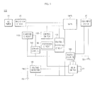
- FIG. 1 is a block diagram of a standby power reduction device according to an embodiment of the present invention and FIG. 2 is a circuit view of the standby power reduction device shown in FIG. 1 .
- the standby power reduction device 100 includes a switching mode power supply (SMPS), a charging circuit 110, a control switch 120, a voltage-dividing circuit 130, a control circuit 140, a hysteresis circuit 150, an electric double layer capacitor (EDLC), a voltage detector 160, a main switch 170, a photo-coupler 180 and a first capacitor C1.
- SMPS switching mode power supply
- EDLC electric double layer capacitor
- the SMPS receives a power voltage V1 rectified from AC power 10 through the rectifier circuit 20 and generates a first output voltage V2 and a second output voltage V3. If a voltage of a sixth terminal 6 is lowered to a preset value or less in a state in which the power voltage V1 is supplied to a first terminal 1 of the SMPS, a voltage difference greater than or equal to the preset value is created between the first terminal 1 and the sixth terminal 6. As a result, the SMPS is operated to generate the first output voltage V2 between a second terminal 2 and a fourth terminal 4 and the second output voltage V3 between a third terminal 3 and a fifth terminal 5.
- the SMPS may stably maintain the first output voltage V2 and the second output voltage V3, irrespective of a voltage variation within a voltage range set between the first terminal 1 and the sixth terminal 6.
- a voltage between the first terminal 1 and the sixth terminal 6 may be set to be in a range of 100 to 300 VDC.
- the second terminal 2 supplies the first output voltage V2 to the equipment device 30, and the third terminal 3 supplies the second output voltage V3 to the charging circuit 110, the control switch 120 and the voltage-dividing circuit 130.
- the fourth terminal 4 of the SMPS is connected to an equipment ground 50, and the fifth terminal 5 is connected to a power ground 40.
- the equipment ground 50 and the power ground 40 are electrically coupled to each other while maintaining a highly insulated state by an insulating transformer included in the SMPS.
- the charging circuit 110 charges the EDLC.
- the charging circuit 110 includes a booster transistor Q1, a first resistor R1, a second resistor R2 and a third resistor R3.
- the booster transistor Q1 receives a charge current from the third terminal 3 of the SMPS and charges the EDLC.
- the first to third resistors R1 to R3 protect the booster transistor Q1 from over-current.
- the control switch 120 controls the main switch 170.
- the control switch 120 includes a first switching transistor Q2 and a fourth resistor R4. If the SMPS is instantaneously operated to then generate the second output voltage V3, a control transistor Q3 is turned on, and if the control transistor Q3 is turned on, the first switching transistor Q2 is turned on. If the first switching transistor Q2 is turned on, a current is allowed to flow to the main switch 170, thereby turning on a second switching transistor Q4 of the main switch 170.
- the voltage-dividing circuit 130 sets an operating point of the control circuit 140.
- the voltage-dividing circuit 130 includes a fifth resistor R5 and a sixth resistor R6 and has the fifth resistor R5 and the sixth resistor R6 connected in series.
- the voltage-dividing circuit 130 receives the second output voltage V3 through the SMPS.
- the voltage-dividing circuit 130 divides the second output voltage V3 to generate a divided voltage VB and supplies the divided voltage VB to the control circuit 140.
- Equation (1) a base current of the control transistor Q3 is ignored.
- VB ⁇ 1 R ⁇ 6 * V ⁇ 3 / R ⁇ 5 + R ⁇ 6
- the second divided voltage VB2 is determined by Equation (2).
- a base current of the control transistor Q3 is ignored.
- V CE2 is a voltage drop between a collector and an emitter when the first switching transistor Q2 is turned on
- V F2 is a forward voltage drop of a first diode D1. Therefore, the second divided voltage VB2 is higher than the first divided voltage VB 1.
- the control circuit 140 controls the charging circuit 110 and the control switch 120.
- the control circuit 140 includes the control transistor Q3. If the control transistor Q3 is turned on, the booster transistor Q1 of the charging circuit 110 and the first switching transistor Q2 of the control switch 120 are turned on. In addition, if the control transistor Q3 is turned off, the booster transistor Q1 of the charging circuit 110 and the first switching transistor Q2 of the control switch 120 are turned off. While the booster transistor Q1 and the first switching transistor Q2 are controlled by the control transistor Q3, they are isolated by the second resistor R2 and the fourth resistor R4, so as not to affect each other.
- a base voltage of the control transistor Q3 is determined by the divided voltage VB of the voltage-dividing circuit 130.
- an emitter voltage of the control transistor Q3 is determined by a charge voltage VC of the EDLC. Therefore, a turned-on or turned-off state of the control transistor Q3 may be determined by a relationship between the divided voltage VB and the voltage VC. That is to say, if a value obtained by subtracting 0.6 V from the divided voltage VB is greater than the charge voltage VC (VB-0.6V > VC), the control transistor Q3 is in a turned-on state.
- 0.6 V is a forward voltage between the base and the emitter, which is required to turn on the control transistor
- 0.6 V is a forward voltage between the base and the emitter, which is required to turn on the control transistor Q3.
- the hysteresis circuit 150 adds a hysteresis characteristic to the control circuit 140.
- the hysteresis circuit 150 includes a first diode D1 and a seventh resistor R7.
- the EDLC stores electric energy.
- the EDLC may store the electric energy through the charging circuit 110.
- the voltage detector 160 is connected in parallel to the EDLC and detects the charge voltage of the EDLC VC. If the charge voltage of the EDLC VC is lower than a lowest charge voltage (VL), the voltage detector 160 operates the main switch 170 using a current flowing from the EDLC. In addition, if the charge voltage of the EDLC VC is higher than the lowest charge voltage VL, the voltage detector 160 interrupts the current from being supplied to the main switch 170
- the main switch 170 drives the SMPS.
- the main switch 170 includes a second switching transistor Q4 and a wired OR circuit.
- the wired OR circuit includes an eighth resistor R8, a ninth resistor R9, a tenth resistor R10 and an eleventh resistor R11.
- the wired OR circuit operates the second switching transistor Q4 by logically summing (ORing) currents supplied from the first switching transistor Q2, the voltage detector 160 and the photo-coupler 180. That is to say, the second switching transistor Q4 is turned off if there is no current supplied from the first switching transistor Q2, the voltage detector 160 and the photo-coupler 170, and is turned on if there is a current supplied from one of the first switching transistor Q2, the voltage detector 160 and the photo-coupler 170.
- the photo-coupler 180 receives a turn-on command from a control circuit (not shown) of a side of the equipment ground 50 and operates the main switch 170 using a current flowing from the EDLC, and interrupts the operation of the main switch 170 by interrupting the current supplied from the EDLC.
- the first capacitor C1 is connected in parallel to the main switch 170 and instantaneously operates the SMPS when a power cord is connected to the AC power 10 for the first time.
- the first capacitor C1 is connected in parallel to the second switching transistor Q4. If an electronic device is connected to the AC power 10 for the first time, the first capacitor C1 is charged and instantaneously operates the SMPS due to over-current. If the charging of the first capacitor C1 is completed after the lapse of a predetermined time, no further over-current flows.
- a charge voltage VC1 of the first capacitor C1 until the first capacitor C1 is fully charged is determined by Equation (4).
- a current IS passing through the first terminal 1 and the sixth terminal 6 of the SMPS is maintained at a fixed value, irrespective of a voltage variation between the first terminal 1 and the sixth terminal 6.
- VC ⁇ 1 IS * t / C where t is a charge time and C is capacitance of the first capacitor C1.
- a sum of a time ton Q3, a time ton Q2 and a time ton Q4 is required, the time ton Q3 taken until a current I Q3 is generated by a base current supplied to the control transistor Q3 and the control transistor Q3 is turned on, the time ton Q2 taken until the first switching transistor Q2 is turned on by the control transistor Q3 to generate a current I Q2 , and the time ton Q4 taken until the second switching transistor Q4 is turned on by the first switching transistor Q2 to generate a current I Q4 .
- Equation (7) tx ⁇ ton SMPS C > tx * IS / V ⁇ 1 - Von
- FIG. 3 is a time chart illustrating an initial operation of the standby power reduction device shown in FIG. 1 .
- the power cord of the electronic device has yet to be connected to the AC power 10, so that the power voltage V1 is 0 V.
- the charge voltage VC is 0 V and the first output voltage V2 and the second output voltage V3 of the SMPS are both 0 V.
- the first capacitor C1 is charged and a current I C1 flows to operate the SMPS.
- the second output voltage V3 has yet to be output. That is to say, a predetermined time is required until the second output voltage V3 is output.
- the SMPS is operated to output the second output voltage V3 and a base current is supplied to the control transistor Q3.
- a time ton Q3 is required.
- control transistor Q3 is turned on to allow the current I Q3 to flow therein.
- a time ton Q2 is required.
- the booster transistor Q1 is turned on by the control transistor Q3 to charge the EDLC.
- the first switching transistor Q2 is turned on to allow the current I Q2 to flow therein.
- a time ton Q4 is required.
- the second switching transistor Q4 is turn on to allow the current I Q4 to flow therein, so that the SMPS is maintained at an operated state by the current I Q4 of the second switching transistor Q4, rather than the current I C1 of the first capacitor C1. If the second switching transistor Q4 is turned on, the current flowing between the first terminal 1 and the sixth terminal 6 of the SMPS is the current I Q4 flowing by the second switching transistor Q4. Thus, the amount of the current I C1 flowing in the first capacitor C1 becomes 0.
- the amount of the current I C1 flowing in the first capacitor C1 becomes 0 at the time t5 before reaching a time t6.
- the second switching transistor Q4 is not turned on until the time t6, the amount of the current I C1 flowing in the first capacitor C1 is reduced, thereby making the SMPS stop operating.
- the standby power reduction device includes a capacitor connected in parallel to a main switch. Therefore, when an electronic device is connected to AC power for the first time, a switching power circuit can be operated using the current flowing in the capacitor.
- FIG. 4 is a time chart illustrating a hysteresis operation of a control transistor.
- control transistor The operation of the control transistor will now be described with reference to FIG. 4 .
- an electric double layer capacitor (EDLC) in a charged state is slowly discharged by the current internally consumed by the standby power reduction device 100, so that it has a charge voltage VC lower than a hysteresis voltage VH1.
- EDLC electric double layer capacitor
- a command instructing the SMPS to be operated is transmitted from a control circuit (not shown) included in the equipment device 30 positioned at a side of the equipment ground 50 to the photo-coupler 180.
- the photo-coupler 180 allows a current to flow from the EDLC to turn on a second switching transistor Q4, thereby maintaining the SMPS at an operated state.
- a first output voltage V2 is supplied to the equipment device 30, so that the equipment device 30 operates.
- a second output voltage V3 is supplied to turn on the control transistor Q3, thereby turning on the booster transistor Q1 and the first switching transistor Q2.
- the current I Q2 is supplied to a base of the second switching transistor Q4.
- the second switching transistor Q4 is not affected by the current I Q2 supplied from the first switching transistor Q2.
- the current is supplied to the voltage-dividing circuit 130 through the hysteresis circuit 150, the divided voltage VB increases to the second divided voltage VB2.
- the charge voltage of the EDLC VC increases to the highest charge voltage VH2. If the charge voltage VC reaches the highest charge voltage VH2, the control transistor Q3 is turned off and the booster transistor Q1 is also turned off, thereby stopping charging of the EDLC. In addition, as the control transistor Q3 is turned off, the first switching transistor Q2 is turned off, so that the current I Q2 of the first switching transistor Q2 is not supplied to the second switching transistor Q4. However, since the current is being supplied to the second switching transistor Q4 from the photo-coupler 180, the second switching transistor Q4 is maintained at a turned-on state.
- the charge voltage of the EDLC VC decreases to reach the hysteresis voltage VH1 to turn on the control transistor Q3 again. Accordingly, the operations performed at the times T1 to T3 are repeated.
- the operations performed at the times T1 to T3 are repeated until the user turns off the power switch to stop using the equipment device 30.
- the current is being supplied from the photo-coupler 180, there are no changes other than stopping and resuming of the charging of the EDLC using the booster transistor Q1.
- the supplying of the current from the photo-coupler 180 is stopped to turn off the second switch transistor Q4. If the second switch transistor Q4 is turned off, the SMPS stops operating, and the charge voltage VC of the EDLC is discharged due to the current internally consumed by the standby power reduction device 100 to slow decrease.
- the voltage detector 160 allows the current to flow from the EDLC to turn on the second switching transistor Q4, thereby operating the SMPS. If the SMPS is operated, the second output voltage V3 is supplied to turn on the control transistor Q3, thereby turning on the booster transistor Q1 and the first switching transistor Q2. If the control transistor Q3 is turned on, the same operation as that performed at the time T1 is performed.
- the booster transistor Q1 If the booster transistor Q1 is turned on to charge the EDLC, the charge voltage VC increases to become higher than the lowest charge voltage VL, so that the voltage detector 160 stops operating, However, since the current of the first switching transistor Q2 is being supplied until the charge voltage VC of the EDLC reaches the highest charge voltage VH2, the second switching transistor Q4 is maintained at a turned-on state.
- the standby power reduction device 100 As described above, in the standby power reduction device 100 according to an embodiment of the present invention, there is no loss in the power measured from the AC power 10 in a standby state of an electronic device without using a starting circuit in a state in which the EDLC is not charged.
- FIG. 5 is a circuit view of a standby power reduction device according to another embodiment of the present invention.
- the standby power reduction device 200 shown in FIG. 5 is substantially the same as the standby power reduction device 100 shown in FIG. 2 , except for a time constant circuit 290. Therefore, the following description will focus on the time constant circuit 290.
- the standby power reduction device 200 includes a switching mode power supply (SMPS), a charging circuit 110, control switch 120, a voltage-dividing circuit 130, a control circuit 140, a hysteresis circuit 150, an electric double layer capacitor (EDLC), a voltage detector 160, a main switch 170, a photo-coupler 180, a first capacitor C1 and a time constant circuit 290.
- SMPS switching mode power supply
- EDLC electric double layer capacitor
- the time constant circuit 290 is electrically connected between the SMPS and the main switch 170.
- the time constant circuit 290 includes a twelfth resistor R12 and a second capacitor C2.
- the time constant circuit 290 turns on a second switching transistor Q4 of the main switch 170 at an early stage, thereby reducing capacitance of the first capacitor C1.
- the time constant circuit 290 supplies an over-current to the second switching transistor Q4 and maintains the second switching transistor Q4 at a turned-on state for a time set by a time constant ( ⁇ ), thereby maintaining the SMPS at an operated state.
- the over-current is not supplied any longer after the lapse of the time set by the time constant ( ⁇ ) from a time at which the second output voltage V3 starts to be supplied.
- the SMPS instantaneously operated by the first capacitor C1 keeps operating under the condition expressed by the following expression of inequality (9): ton Q ⁇ 3 + ton Q ⁇ 2 ⁇ ⁇ where ton Q3 is a turn-on time of the control transistor Q3 and ton Q2 is a turn-on time of the first switching transistor Q2.
- the SMPS can be maintained at the operated state by setting the time constant( ⁇ ) of the time constant circuit 290 to be greater than a time required to make both of the control transistor Q3 and the first switching transistor Q2 turned on.
- FIG. 6 is a time chart illustrating an initial operation of the standby power reduction device shown in FIG. 5 .
- a power voltage V1 is 0 V.
- the charge voltage VC is 0 V and a first output voltage V2 and a second output voltage V3 of the SMPS are both 0 V.
- the first capacitor C1 is charged and a current I C1 flows to operate the SMPS.
- the second output voltage V3 has yet to be output. That is to say, a predetermined time is required until the second output voltage V3 is output.
- the SMPS is operated to output the second output voltage V3 and a base current is supplied to the control transistor Q3.
- a time ton Q3 is required. If the second output voltage V3 is supplied to the time constant circuit 290, an over-current I C2 is supplied to the second switching transistor Q4 for a time set by the time constant( ⁇ ) of the time constant circuit 290. However, in order to turn on the second switching transistor Q4, a time ton Q4 is required.
- the second switching transistor Q4 is turned on to allow a current I Q4 to flow, so that the SMPS is maintained at an operated state. If the second switching transistor Q4 is turned on, no current flows in the first capacitor C1.
- the amount of the current I C1 flowing in the first capacitor C1 becomes 0 at the time t3 before reaching a time t4.
- the second switching transistor Q4 is not turned on until the time t4
- the amount of the current I C1 flowing in the first capacitor C1 is reduced, thereby making the SMPS stop operating.
- the booster transistor Q1 is turned on by the current of the control transistor Q3 to charge the EDLC.
- the first switching transistor Q2 is turned on to supply the current to the second switching transistor Q4.
- the second switching transistor Q4 is maintained at a turned-on state by the current I C2 supplied by the time constant circuit 290.
- the amount of the current I C2 supplied by the time constant circuit 290 is reduced to reach so low a level of current that the second switching transistor Q4 cannot be maintained at the turned-on state.
- the second switching transistor Q4 is maintained at the turned-on state.
- the standby power reduction device 200 includes the time constant circuit 290 to reduce capacitance of the first capacitor C1, thereby reducing the cost.
- FIG. 7 is a circuit view of a standby power reduction device shown according to still another embodiment of the present invention.
- the standby power reduction device 300 shown in FIG. 7 is substantially the same as the standby power reduction device 100 shown in FIG. 2 , except for a time constant circuit 390.
- the first capacitor C1 is not provided in the standby power reduction device 300 shown in FIG. 7 . Therefore, the following description will focus on the time constant circuit 390.
- the standby power reduction device 300 includes a switching mode power supply (SMPS), a charging circuit 110, a control switch 120, a voltage-dividing circuit 130, a control circuit 140, a hysteresis circuit 150, an electric double layer capacitor (EDLC), a voltage detector 160, a main switch 170, a photo-coupler 180 and a time constant circuit 390.
- SMPS switching mode power supply
- EDLC electric double layer capacitor
- the time constant circuit 390 is electrically connected between the rectifier circuit 20 and the main switch 170.
- the time constant circuit 390 includes a thirteenth resistor R13 and a third capacitor C3. Since the time constant circuit 390 is directly connected to the main switch 170 from an output of the rectifier circuit 20, an over-current is supplied to the second switching transistor Q4 as soon as a power cord of an electronic device is connected to AC power 10. Therefore, it is not necessary to provide a first capacitor connected in parallel to the second switching transistor Q4.
- the time constant circuit 390 supplies the over-current to the second switching transistor Q as soon as a power voltage V1 is supplied, thereby turning on the second switching transistor Q4 for a time set by a time constant(T) and maintaining the SMPS at an operated state.
- FIG. 8 is a time chart illustrating an initial operation of the standby power reduction device shown in FIG. 7 .
- the power cord of the electronic device has yet to be connected to the AC power 10, so that a power voltage V1 is 0 V.
- the charge voltage VC is 0 V and a first output voltage V2 and a second output voltage V3 of the SMPS are both 0 V.
- the power cord of the electronic device is connected to the AC power 10 for the first time, the power voltage V1 is supplied to the SMPS and the time constant circuit 390. If the power voltage V1 is supplied to the time constant circuit 390, an over-current I C3 is supplied to the second switching transistor Q4 for a time set by the time constant ( ⁇ ). However, in order to turn on the second switching transistor Q4, a time ton Q4 is required.
- the second switching transistor Q4 is turned on to allow a current I Q4 to flow therein, thereby operating the SMPS.
- the second output voltage V3 has yet to be output. That is to say, a predetermined time is required until the second output voltage V3 is output.
- the SMPS starts to be operated to supply the second output voltage V3 to the control transistor Q3.
- a time ton Q3 is required.
- the control transistor Q3 is turned on to supply the current I Q3 to the booster transistor Q1 and the first switching transistor Q2.
- a time ton Q1 is required.
- a time ton Q2 is required.
- the first switching transistor Q2 is turned on to supply the current I Q2 to the second switching transistor Q4.
- the second switching transistor Q4 is maintained at a turned-on state.
- the amount of the current I C3 supplied by the time constant circuit 390 is reduced to reach so low a level of current that the second switching transistor Q4 cannot be maintained at the turned-on state.
- the second switching transistor Q4 is maintained at the turned-on state.
- the standby power reduction device 300 includes the time constant circuit 390 electrically connected between the rectifier circuit 20 and the main switch 170, it is not necessary to provide the first capacitor connected in parallel to the main switch 170.
- a standby power reduction device including a capacitor connected in parallel to a main switch controlling a switching mode power supply, without the necessity of providing a starting circuit, thereby reducing the cost and enabling miniaturization of product.
- the standby power reduction device includes a switching mode power supply (SMPS) receiving a power voltage rectified from AC power and generating a first output voltage and a second output voltage, a voltage-dividing circuit electrically connected to the SMPS, receiving the second output voltage and generating a divided voltage, a control circuit electrically connected to the voltage-dividing circuit, operated by the divided voltage and including a control transistor, a charging circuit electrically connected to the control circuit, operated by the control circuit and including a booster transistor, an EDLC electrically connected to the charging circuit and charging electric energy by the charging circuit, a voltage detector connected in parallel to the EDLC and detecting a charge voltage of the EDLC, a control switch electrically connected to the control circuit, operated by the control circuit and including a first switching transistor, a main switch operated by the control switch, controlling
Landscapes
- Engineering & Computer Science (AREA)
- Power Engineering (AREA)
- Emergency Management (AREA)
- Business, Economics & Management (AREA)
- Electromagnetism (AREA)
- Physics & Mathematics (AREA)
- Life Sciences & Earth Sciences (AREA)
- General Physics & Mathematics (AREA)
- Radar, Positioning & Navigation (AREA)
- Automation & Control Theory (AREA)
- Sustainable Energy (AREA)
- Sustainable Development (AREA)
- Dc-Dc Converters (AREA)
- Charge And Discharge Circuits For Batteries Or The Like (AREA)
Abstract
Description
- Aspects of the present invention relate to a standby power reduction device.
- In general, a standby power reduction device using an electric double layer capacitor (EDLC) charges electric energy in the EDLC having a large capacity and the electric energy charged in the EDLC is used in a lowest amount of electric energy required in a standby state in which no electric device is used. Therefore, AC power is completely interrupted during a standby time of an electronic device, thereby reducing a loss in the standby power supplied from the AC power.
- Meanwhile, when an electronic device is forwarded from a factory to be connected to AC power for the first time, when AC power is replenished after long-time power interruption, or when AC power is reconnected after long-time disconnection, EDLC may be discharged and it is not possible to start the electronic device.
- Therefore, it is necessary to provide a starting circuit capable of starting the SMPS by sensing the AC power supplied for the first time. However, since the starting circuit operates just one time when a power cord is connected to AC power for the first time but does not perform any function while the electronic device is driven. Therefore, the starting circuit may increase the cost and may make it difficult to achieve miniaturization of product.
- Aspects of the present invention provide a standby power reduction device, which can reduce the cost and enables miniaturization of product.
- In accordance with one aspect of the present invention, there is provided a standby power reduction device including a switching mode power supply (SMPS) receiving a power voltage rectified from AC power and generating a first output voltage and a second output voltage, a voltage-dividing circuit electrically connected to the SMPS, receiving the second output voltage and generating a divided voltage, a control circuit electrically connected to the voltage-dividing circuit, operated by the divided voltage and including a control transistor, a charging circuit electrically connected to the control circuit, operated by the control circuit and including a booster transistor, an electric double layer capacitor (EDLC) electrically connected to the charging circuit and charging electric energy by the charging circuit, a voltage detector connected in parallel to the EDLC and detecting a charge voltage of the EDLC, a control switch electrically connected to the control circuit, operated by the control circuit and including a first switching transistor, a main switch operated by the control switch, controlling the operation of the SMPS and including a second switching transistor and a wired OR circuit, a photo-coupler controlling the operation of the main switch according to a command of a device operated by a first output voltage, and a first capacitor connected in parallel to the second switching transistor of the main switch, wherein the first capacitor operates the SMPS using a current flowing in the first capacitor when an electronic device is connected to the AC power for the first time.
- The second switching transistor may be operated by logically summing (ORing) on an output of the photo-coupler, an output of the voltage detector and an output of the control circuit.
- If the charge voltage is lower than a lowest charge voltage, the voltage detector may operate the main switch.
- A base voltage of the control transistor may be determined by the divided voltage and an emitter voltage of the control transistor may be determined by the charge voltage of the EDLC.
- The standby power reduction device may further include a hysteresis circuit connected between the voltage-dividing circuit and the control switch. Here, the hysteresis circuit adds a hysteresis characteristic to the control circuit.
- If the charge voltage of the EDLC reaches a hysteresis voltage, the control transistor may be turned on to charge the EDLC by turning on the booster transistor, and if the charge voltage of the EDLC reaches a highest charge voltage, the control transistor may be turned off to stop charging the EDLC by turning off the booster transistor.
- The hysteresis voltage may be a voltage obtained by subtracting 0.6 V that is a forward base-emitter voltage required to turn on the control transistor from the divided voltage that is a voltage when the control transistor is in a turned-off state.
- The highest charge voltage may be a voltage obtained by subtracting 0.6 V that is a forward base-emitter voltage required to turn on the control transistor from the divided voltage that is a voltage when the control transistor is in a turned-on state.
- If the control transistor is turned on, the booster transistor and the first switching transistor may be turned on, and if the control transistor is turned off, the booster transistor and the first switching transistor may be turned off.
- If the first switching transistor is turned on, the second switching transistor may be turned on to maintain the SMPS at an operated state.
- A time constant determined by an amount of current passing through the first capacitor and the SMPS may be greater than a time required until the second switching transistor is turned on by the second output voltage.
- The standby power reduction device may further include a time constant circuit electrically connected between an output terminal of the SMPS and the main switch. Here, the time constant circuit has a resistor and a second capacitor connected in series.
- If the second output voltage is generated, the time constant circuit may reduce capacitance of the first capacitor by turning on the second switching transistor.
- The time constant of the time constant circuit may be set to be greater than a sum of a time required to turn on the control transistor and a time required to turn on the first switching transistor.
- In accordance with another aspect of the present invention, there is provided a standby power reduction device including a switching mode power supply (SMPS) receiving a power voltage rectified from AC power and generating a first output voltage and a second output voltage; a voltage-dividing circuit electrically connected to the SMPS, receiving the second output voltage and generating a divided voltage; a control circuit electrically connected to the voltage-dividing circuit, operated by the divided voltage and including a control transistor; a charging circuit electrically connected to the control circuit, operated by the control circuit and including a booster transistor; an electric double layer capacitor (EDLC) electrically connected to the charging circuit and charging electric energy by the charging circuit; a voltage detector connected in parallel to the EDLC and detecting a charge voltage of the EDLC; a control switch electrically connected to the control circuit, operated by the control circuit and including a first switching transistor; a main switch operated by the control switch, controlling the operation of the SMPS and including a second switching transistor and a wired OR circuit; a photo-coupler controlling the operation of the main switch according to a command of a device operated by a first output voltage; and a time constant circuit electrically connected between an input terminal of the SMPS and the main switch, wherein the time constant circuit operates the SMPS using a current flowing in the time constant circuit when an electronic device is connected to the AC power for the first time.
- The time constant of the time constant circuit may be set to be greater than a sum of a time required to turn on the control transistor and a time required to turn on the first switching transistor.
- The second switching transistor may be operated by logically summing (ORing) on an output of the photo-coupler, an output of the voltage detector, an output of the control circuit and an output of the time constant circuit.
- As described above, since the standby power reduction device according to the embodiment of the present invention includes a capacitor connected in parallel to a main switch, a switching mode power supply can drive using a current flowing in the capacitor when an electronic device is connected to AC power for the first time.
- Accordingly, the standby power reduction device according to the embodiment of the present invention may have no loss in the power measured from AC power when the electronic device is in a standby state without using a starting circuit in a state in which the EDLC is not charged.
- Additional aspects and/or advantages of the invention will be set forth in part in the description which follows and, in part, will be obvious from the description, or may be learned by practice of the invention.
- The objects, features and advantages of the present invention will be more apparent from the following detailed description in conjunction with the accompanying drawings, in which:
-
FIG. 1 is a block diagram of a standby power reduction device according to an embodiment of the present invention; -
FIG. 2 is a circuit view of the standby power reduction device shown inFIG. 1 ; -
FIG. 3 is a time chart illustrating an initial operation of the standby power reduction device shown inFIG. 1 ; -
FIG. 4 is a time chart illustrating a hysteresis operation of a control transistor; -
FIG. 5 is a circuit view of a standby power reduction device shown according to another embodiment of the present invention; -
FIG. 6 is a time chart illustrating an initial operation of the standby power reduction device shown inFIG. 5 ; -
FIG. 7 is a circuit view of a standby power reduction device shown according to still another embodiment of the present invention; and -
FIG. 8 is a time chart illustrating an initial operation of the standby power reduction device shown inFIG. 7 . - Hereinafter, examples of embodiments of the invention will be described in detail with reference to the accompanying drawings such that they can easily be made and used by those skilled in the art.
- Like numbers refer to like elements throughout. In addition, it will be understood that when an element or layer is referred to as being "electrically connected to" another element or layer, it can be directly connected to the other element or layer or intervening elements or layers may be present.
-
FIG. 1 is a block diagram of a standby power reduction device according to an embodiment of the present invention andFIG. 2 is a circuit view of the standby power reduction device shown inFIG. 1 . - Referring to
FIGS. 1 and2 , the standbypower reduction device 100 according to an embodiment of the present invention includes a switching mode power supply (SMPS), acharging circuit 110, acontrol switch 120, a voltage-dividingcircuit 130, acontrol circuit 140, ahysteresis circuit 150, an electric double layer capacitor (EDLC), avoltage detector 160, amain switch 170, a photo-coupler 180 and a first capacitor C1. - The SMPS receives a power voltage V1 rectified from
AC power 10 through therectifier circuit 20 and generates a first output voltage V2 and a second output voltage V3. If a voltage of asixth terminal 6 is lowered to a preset value or less in a state in which the power voltage V1 is supplied to afirst terminal 1 of the SMPS, a voltage difference greater than or equal to the preset value is created between thefirst terminal 1 and thesixth terminal 6. As a result, the SMPS is operated to generate the first output voltage V2 between asecond terminal 2 and afourth terminal 4 and the second output voltage V3 between athird terminal 3 and afifth terminal 5. The SMPS may stably maintain the first output voltage V2 and the second output voltage V3, irrespective of a voltage variation within a voltage range set between thefirst terminal 1 and thesixth terminal 6. Here, a voltage between thefirst terminal 1 and thesixth terminal 6 may be set to be in a range of 100 to 300 VDC. If the SMPS is operated, thesecond terminal 2 supplies the first output voltage V2 to theequipment device 30, and thethird terminal 3 supplies the second output voltage V3 to thecharging circuit 110, thecontrol switch 120 and the voltage-dividingcircuit 130. Thefourth terminal 4 of the SMPS is connected to anequipment ground 50, and thefifth terminal 5 is connected to apower ground 40. Here, the equipment ground 50 and thepower ground 40 are electrically coupled to each other while maintaining a highly insulated state by an insulating transformer included in the SMPS. - The
charging circuit 110 charges the EDLC. Thecharging circuit 110 includes a booster transistor Q1, a first resistor R1, a second resistor R2 and a third resistor R3. The booster transistor Q1 receives a charge current from thethird terminal 3 of the SMPS and charges the EDLC. The first to third resistors R1 to R3 protect the booster transistor Q1 from over-current. - The
control switch 120 controls themain switch 170. Thecontrol switch 120 includes a first switching transistor Q2 and a fourth resistor R4. If the SMPS is instantaneously operated to then generate the second output voltage V3, a control transistor Q3 is turned on, and if the control transistor Q3 is turned on, the first switching transistor Q2 is turned on. If the first switching transistor Q2 is turned on, a current is allowed to flow to themain switch 170, thereby turning on a second switching transistor Q4 of themain switch 170. - The voltage-dividing
circuit 130 sets an operating point of thecontrol circuit 140. The voltage-dividingcircuit 130 includes a fifth resistor R5 and a sixth resistor R6 and has the fifth resistor R5 and the sixth resistor R6 connected in series. The voltage-dividingcircuit 130 receives the second output voltage V3 through the SMPS. The voltage-dividingcircuit 130 divides the second output voltage V3 to generate a divided voltage VB and supplies the divided voltage VB to thecontrol circuit 140. - Meanwhile, when the control transistor Q3 of the
control circuit 140 is turned off, the first divided voltage VB1 is determined by Equation (1). Here, a base current of the control transistor Q3 is ignored.
- In addition, when the control transistor Q3 of the
control circuit 140 is turned on, the second divided voltage VB2 is determined by Equation (2). Here, a base current of the control transistor Q3 is ignored.

Therefore, the second divided voltage VB2 is higher than the first dividedvoltage VB 1. - The
control circuit 140 controls the chargingcircuit 110 and thecontrol switch 120. Thecontrol circuit 140 includes the control transistor Q3. If the control transistor Q3 is turned on, the booster transistor Q1 of the chargingcircuit 110 and the first switching transistor Q2 of thecontrol switch 120 are turned on. In addition, if the control transistor Q3 is turned off, the booster transistor Q1 of the chargingcircuit 110 and the first switching transistor Q2 of thecontrol switch 120 are turned off. While the booster transistor Q1 and the first switching transistor Q2 are controlled by the control transistor Q3, they are isolated by the second resistor R2 and the fourth resistor R4, so as not to affect each other. - A base voltage of the control transistor Q3 is determined by the divided voltage VB of the voltage-dividing
circuit 130. In addition, an emitter voltage of the control transistor Q3 is determined by a charge voltage VC of the EDLC. Therefore, a turned-on or turned-off state of the control transistor Q3 may be determined by a relationship between the divided voltage VB and the voltage VC. That is to say, if a value obtained by subtracting 0.6 V from the divided voltage VB is greater than the charge voltage VC (VB-0.6V > VC), the control transistor Q3 is in a turned-on state. In addition, if a value obtained by subtracting 0.6 V from the divided voltage VB is smaller than the charge voltage VC (VB-0.6V < VC), the control transistor Q3 is in a turned-off state. Here, 0.6 V is a forward voltage between the base and the emitter, which is required to turn on the control transistor - Q3.
- Based on the above-stated finding, a hysteresis voltage (VH1) and a highest charge voltage (VH2) may be set by Equation (3) as follows:


- The
hysteresis circuit 150 adds a hysteresis characteristic to thecontrol circuit 140. Thehysteresis circuit 150 includes a first diode D1 and a seventh resistor R7. - The EDLC stores electric energy. The EDLC may store the electric energy through the charging
circuit 110. - The
voltage detector 160 is connected in parallel to the EDLC and detects the charge voltage of the EDLC VC. If the charge voltage of the EDLC VC is lower than a lowest charge voltage (VL), thevoltage detector 160 operates themain switch 170 using a current flowing from the EDLC. In addition, if the charge voltage of the EDLC VC is higher than the lowest charge voltage VL, thevoltage detector 160 interrupts the current from being supplied to themain switch 170 - The
main switch 170 drives the SMPS. Themain switch 170 includes a second switching transistor Q4 and a wired OR circuit. The wired OR circuit includes an eighth resistor R8, a ninth resistor R9, a tenth resistor R10 and an eleventh resistor R11. The wired OR circuit operates the second switching transistor Q4 by logically summing (ORing) currents supplied from the first switching transistor Q2, thevoltage detector 160 and the photo-coupler 180. That is to say, the second switching transistor Q4 is turned off if there is no current supplied from the first switching transistor Q2, thevoltage detector 160 and the photo-coupler 170, and is turned on if there is a current supplied from one of the first switching transistor Q2, thevoltage detector 160 and the photo-coupler 170. - The photo-
coupler 180 receives a turn-on command from a control circuit (not shown) of a side of theequipment ground 50 and operates themain switch 170 using a current flowing from the EDLC, and interrupts the operation of themain switch 170 by interrupting the current supplied from the EDLC. - The first capacitor C1 is connected in parallel to the
main switch 170 and instantaneously operates the SMPS when a power cord is connected to theAC power 10 for the first time. In detail, the first capacitor C1 is connected in parallel to the second switching transistor Q4. If an electronic device is connected to theAC power 10 for the first time, the first capacitor C1 is charged and instantaneously operates the SMPS due to over-current. If the charging of the first capacitor C1 is completed after the lapse of a predetermined time, no further over-current flows. - A charge voltage VC1 of the first capacitor C1 until the first capacitor C1 is fully charged is determined by Equation (4). Here, it is assumed that a current IS passing through the
first terminal 1 and thesixth terminal 6 of the SMPS is maintained at a fixed value, irrespective of a voltage variation between thefirst terminal 1 and thesixth terminal 6.
- Therefore, the minimum voltage Von between the
first terminal 1 and thesixth terminal 6, by which the SMPS is continuously operated, and a time (ton(SMPS) in which the SMPS can be continuously operated by the first capacitor C1, is determined by Equation (5):
- In order to keep the SMPS operating, irrespective of the first capacitor C1, a sum of a time ton Q3, a time ton Q2 and a time ton Q4 is required, the time ton Q3 taken until a current IQ3 is generated by a base current supplied to the control transistor Q3 and the control transistor Q3 is turned on, the time ton Q2 taken until the first switching transistor Q2 is turned on by the control transistor Q3 to generate a current IQ2, and the time ton Q4 taken until the second switching transistor Q4 is turned on by the first switching transistor Q2 to generate a current IQ4. That is to say, a time tx required to maintain the SMPS at the operated state by the second switching transistor Q4 from a time at which the base current is supplied to the control transistor Q3 after the SMPS is instantaneously operated to generate the second output voltage V1, is determined by Equation (6):

- Accordingly, in order to make the standby
power reduction device 100 smoothly operate, the following Equation (7) should be satisfied:

-
FIG. 3 is a time chart illustrating an initial operation of the standby power reduction device shown inFIG. 1 . - An initial operation of the aforementioned standby
power reduction device 100 will now be described with reference toFIG. 3 . - At a time t0, the power cord of the electronic device has yet to be connected to the
AC power 10, so that the power voltage V1 is 0 V. In addition, since the EDLC has yet to be charged, the charge voltage VC is 0 V and the first output voltage V2 and the second output voltage V3 of the SMPS are both 0 V. - At a time t1, if the power cord of the electronic device is connected to the
AC power 10 for the first time, the first capacitor C1 is charged and a current IC1 flows to operate the SMPS. However, the second output voltage V3 has yet to be output. That is to say, a predetermined time is required until the second output voltage V3 is output. - At a time t2, the SMPS is operated to output the second output voltage V3 and a base current is supplied to the control transistor Q3. Here, in order to turn on the control transistor Q3, a time ton Q3 is required.
- At a time t3, the control transistor Q3 is turned on to allow the current IQ3 to flow therein. However, in order to turn on the first switching transistor Q2, a time ton Q2 is required.
- At a time t4, the booster transistor Q1 is turned on by the control transistor Q3 to charge the EDLC. In addition, the first switching transistor Q2 is turned on to allow the current IQ2 to flow therein. However, in order to turn on the second switching transistor Q4, a time ton Q4 is required.
- At a time t5, the second switching transistor Q4 is turn on to allow the current IQ4 to flow therein, so that the SMPS is maintained at an operated state by the current IQ4 of the second switching transistor Q4, rather than the current IC1 of the first capacitor C1. If the second switching transistor Q4 is turned on, the current flowing between the
first terminal 1 and thesixth terminal 6 of the SMPS is the current IQ4 flowing by the second switching transistor Q4. Thus, the amount of the current IC1 flowing in the first capacitor C1 becomes 0. - As stated above, the amount of the current IC1 flowing in the first capacitor C1 becomes 0 at the time t5 before reaching a time t6. However, if the second switching transistor Q4 is not turned on until the time t6, the amount of the current IC1 flowing in the first capacitor C1 is reduced, thereby making the SMPS stop operating.
- As described above, the standby power reduction device according to an embodiment of the present invention includes a capacitor connected in parallel to a main switch. Therefore, when an electronic device is connected to AC power for the first time, a switching power circuit can be operated using the current flowing in the capacitor.
-
FIG. 4 is a time chart illustrating a hysteresis operation of a control transistor. - The operation of the control transistor will now be described with reference to
FIG. 4 . - At a time T0, an electric double layer capacitor (EDLC) in a charged state is slowly discharged by the current internally consumed by the standby
power reduction device 100, so that it has a charge voltage VC lower than a hysteresis voltage VH1. - At a time T1, if a user turns on a power switch to use an
equipment device 30, a command instructing the SMPS to be operated is transmitted from a control circuit (not shown) included in theequipment device 30 positioned at a side of theequipment ground 50 to the photo-coupler 180. The photo-coupler 180 allows a current to flow from the EDLC to turn on a second switching transistor Q4, thereby maintaining the SMPS at an operated state. If the SMPS is operated, a first output voltage V2 is supplied to theequipment device 30, so that theequipment device 30 operates. In addition, if the SMPS is operated, a second output voltage V3 is supplied to turn on the control transistor Q3, thereby turning on the booster transistor Q1 and the first switching transistor Q2. If the first switching transistor Q2 is turned on, the current IQ2 is supplied to a base of the second switching transistor Q4. However, since a current is being supplied to the second switching transistor Q4 from the photo-coupler 180, the second switching transistor Q4 is not affected by the current IQ2 supplied from the first switching transistor Q2. In addition, according to the flow of the current IQ2 supplied from the first switching transistor Q2, the current is supplied to the voltage-dividingcircuit 130 through thehysteresis circuit 150, the divided voltage VB increases to the second divided voltage VB2. - At a time T2, the charge voltage of the EDLC VC increases to the highest charge voltage VH2. If the charge voltage VC reaches the highest charge voltage VH2, the control transistor Q3 is turned off and the booster transistor Q1 is also turned off, thereby stopping charging of the EDLC. In addition, as the control transistor Q3 is turned off, the first switching transistor Q2 is turned off, so that the current IQ2 of the first switching transistor Q2 is not supplied to the second switching transistor Q4. However, since the current is being supplied to the second switching transistor Q4 from the photo-
coupler 180, the second switching transistor Q4 is maintained at a turned-on state. In addition, since the current IQ2 of the first switching transistor Q2 does not flow, supplying of the current through thehysteresis circuit 150 is stopped, so that the divided voltage VB decreases to reach a level of the first divided voltage VB1. In addition, since the EDLC stops being charged, a level of the charge voltage VC is slowly lowered. - At a time T3, the charge voltage of the EDLC VC decreases to reach the hysteresis voltage VH1 to turn on the control transistor Q3 again. Accordingly, the operations performed at the times T1 to T3 are repeated.
- Here, the operations performed at the times T1 to T3 are repeated until the user turns off the power switch to stop using the
equipment device 30. However, since the current is being supplied from the photo-coupler 180, there are no changes other than stopping and resuming of the charging of the EDLC using the booster transistor Q1. - At a time Tn, if the user turns off the power switch to stop using the
equipment device 30, the supplying of the current from the photo-coupler 180 is stopped to turn off the second switch transistor Q4. If the second switch transistor Q4 is turned off, the SMPS stops operating, and the charge voltage VC of the EDLC is discharged due to the current internally consumed by the standbypower reduction device 100 to slow decrease. - At a time (Tn+1), if the charge voltage VC reaches the lowest charge voltage VL, the
voltage detector 160 allows the current to flow from the EDLC to turn on the second switching transistor Q4, thereby operating the SMPS. If the SMPS is operated, the second output voltage V3 is supplied to turn on the control transistor Q3, thereby turning on the booster transistor Q1 and the first switching transistor Q2. If the control transistor Q3 is turned on, the same operation as that performed at the time T1 is performed. If the booster transistor Q1 is turned on to charge the EDLC, the charge voltage VC increases to become higher than the lowest charge voltage VL, so that thevoltage detector 160 stops operating, However, since the current of the first switching transistor Q2 is being supplied until the charge voltage VC of the EDLC reaches the highest charge voltage VH2, the second switching transistor Q4 is maintained at a turned-on state. - At a time (Tn+2), if the charge voltage of the EDLC VC reaches the highest charge voltage VH2, the control transistor Q3 is turned off to make the EDLC stop being charged, and the charge voltage of the EDLC VC is discharged due to the current internally consumed by the standby
power reduction device 100 to then slowly decrease. - As described above, in the standby
power reduction device 100 according to an embodiment of the present invention, there is no loss in the power measured from theAC power 10 in a standby state of an electronic device without using a starting circuit in a state in which the EDLC is not charged. -
FIG. 5 is a circuit view of a standby power reduction device according to another embodiment of the present invention. - The standby
power reduction device 200 shown inFIG. 5 is substantially the same as the standbypower reduction device 100 shown inFIG. 2 , except for a timeconstant circuit 290. Therefore, the following description will focus on the timeconstant circuit 290. - Referring to
FIG. 5 , the standbypower reduction device 200 according to another embodiment of the present invention includes a switching mode power supply (SMPS), a chargingcircuit 110,control switch 120, a voltage-dividingcircuit 130, acontrol circuit 140, ahysteresis circuit 150, an electric double layer capacitor (EDLC), avoltage detector 160, amain switch 170, a photo-coupler 180, a first capacitor C1 and a timeconstant circuit 290. - The time
constant circuit 290 is electrically connected between the SMPS and themain switch 170. The timeconstant circuit 290 includes a twelfth resistor R12 and a second capacitor C2. The timeconstant circuit 290 turns on a second switching transistor Q4 of themain switch 170 at an early stage, thereby reducing capacitance of the first capacitor C1. - As soon as a second output voltage V3 of the SMPS is supplied, the time
constant circuit 290 supplies an over-current to the second switching transistor Q4 and maintains the second switching transistor Q4 at a turned-on state for a time set by a time constant (τ), thereby maintaining the SMPS at an operated state. The over-current is not supplied any longer after the lapse of the time set by the time constant (τ) from a time at which the second output voltage V3 starts to be supplied. The time constant(τ) of the timeconstant circuit 290 is determined by Equation (8).
- Therefore, the SMPS instantaneously operated by the first capacitor C1 keeps operating under the condition expressed by the following expression of inequality (9):

- That is to say, the SMPS can be maintained at the operated state by setting the time constant(τ) of the time
constant circuit 290 to be greater than a time required to make both of the control transistor Q3 and the first switching transistor Q2 turned on. -
FIG. 6 is a time chart illustrating an initial operation of the standby power reduction device shown inFIG. 5 . - The operation of the standby power reduction device according to another embodiment of the present invention will now be described in detail with reference to
FIG. 6 . - At a time t0, since a power cord of the electronic device has yet to be connected to an
AC power 10, so that a power voltage V1 is 0 V. In addition, since the EDLC has yet to be charged, the charge voltage VC is 0 V and a first output voltage V2 and a second output voltage V3 of the SMPS are both 0 V. - At a time t1, if the power cord of the electronic device is connected to the
AC power 10 for the first time, the first capacitor C1 is charged and a current IC1 flows to operate the SMPS. However, the second output voltage V3 has yet to be output. That is to say, a predetermined time is required until the second output voltage V3 is output. - At a time t2, the SMPS is operated to output the second output voltage V3 and a base current is supplied to the control transistor Q3. Here, in order to turn on the control transistor Q3, a time ton Q3 is required. If the second output voltage V3 is supplied to the time
constant circuit 290, an over-current IC2 is supplied to the second switching transistor Q4 for a time set by the time constant(τ) of the timeconstant circuit 290. However, in order to turn on the second switching transistor Q4, a time ton Q4 is required. - At a time t3, the second switching transistor Q4 is turned on to allow a current IQ4 to flow, so that the SMPS is maintained at an operated state. If the second switching transistor Q4 is turned on, no current flows in the first capacitor C1.
- As stated above, the amount of the current IC1 flowing in the first capacitor C1 becomes 0 at the time t3 before reaching a time t4. However, if the second switching transistor Q4 is not turned on until the time t4, the amount of the current IC1 flowing in the first capacitor C1 is reduced, thereby making the SMPS stop operating.
- At a time t5, the booster transistor Q1 is turned on by the current of the control transistor Q3 to charge the EDLC. In addition, the first switching transistor Q2 is turned on to supply the current to the second switching transistor Q4. However, the second switching transistor Q4 is maintained at a turned-on state by the current IC2 supplied by the time
constant circuit 290. - At a time t6, the amount of the current IC2 supplied by the time
constant circuit 290 is reduced to reach so low a level of current that the second switching transistor Q4 cannot be maintained at the turned-on state. However, since the current IC2 of the first switching transistor Q2 is being supplied, the second switching transistor Q4 is maintained at the turned-on state. - As described above, the standby
power reduction device 200 includes the timeconstant circuit 290 to reduce capacitance of the first capacitor C1, thereby reducing the cost. -
FIG. 7 is a circuit view of a standby power reduction device shown according to still another embodiment of the present invention. - The standby
power reduction device 300 shown inFIG. 7 is substantially the same as the standbypower reduction device 100 shown inFIG. 2 , except for a timeconstant circuit 390. In addition, unlike in the standbypower reduction device 100 shown inFIG. 2 , the first capacitor C1 is not provided in the standbypower reduction device 300 shown inFIG. 7 . Therefore, the following description will focus on the timeconstant circuit 390. - Referring to
FIG. 7 , the standbypower reduction device 300 according to still another embodiment of the present invention includes a switching mode power supply (SMPS), a chargingcircuit 110, acontrol switch 120, a voltage-dividingcircuit 130, acontrol circuit 140, ahysteresis circuit 150, an electric double layer capacitor (EDLC), avoltage detector 160, amain switch 170, a photo-coupler 180 and a timeconstant circuit 390. - The time
constant circuit 390 is electrically connected between therectifier circuit 20 and themain switch 170. The timeconstant circuit 390 includes a thirteenth resistor R13 and a third capacitor C3. Since the timeconstant circuit 390 is directly connected to themain switch 170 from an output of therectifier circuit 20, an over-current is supplied to the second switching transistor Q4 as soon as a power cord of an electronic device is connected toAC power 10. Therefore, it is not necessary to provide a first capacitor connected in parallel to the second switching transistor Q4. - The time
constant circuit 390 supplies the over-current to the second switching transistor Q as soon as a power voltage V1 is supplied, thereby turning on the second switching transistor Q4 for a time set by a time constant(T) and maintaining the SMPS at an operated state. -
FIG. 8 is a time chart illustrating an initial operation of the standby power reduction device shown inFIG. 7 . - The operation of the standby power reduction device according to still another embodiment of the present invention will now be described in detail with reference to
FIG. 8 . - At a time t0, the power cord of the electronic device has yet to be connected to the
AC power 10, so that a power voltage V1 is 0 V. In addition, since the EDLC has yet to be charged, the charge voltage VC is 0 V and a first output voltage V2 and a second output voltage V3 of the SMPS are both 0 V. - At a time t1, the power cord of the electronic device is connected to the
AC power 10 for the first time, the power voltage V1 is supplied to the SMPS and the timeconstant circuit 390. If the power voltage V1 is supplied to the timeconstant circuit 390, an over-current IC3 is supplied to the second switching transistor Q4 for a time set by the time constant (τ). However, in order to turn on the second switching transistor Q4, a time ton Q4 is required. - At a time t2, the second switching transistor Q4 is turned on to allow a current IQ4 to flow therein, thereby operating the SMPS. However, the second output voltage V3 has yet to be output. That is to say, a predetermined time is required until the second output voltage V3 is output.
- At a time t3, the SMPS starts to be operated to supply the second output voltage V3 to the control transistor Q3. However, in order to turn on the control transistor Q3, a time ton Q3 is required.
- At a time t4, the control transistor Q3 is turned on to supply the current IQ3 to the booster transistor Q1 and the first switching transistor Q2. However, in order to turn on the booster transistor Q1, a time ton Q1 is required. In addition, in order to turn on the first switching transistor Q2, a time ton Q2 is required.
- At a time t5, the first switching transistor Q2 is turned on to supply the current IQ2 to the second switching transistor Q4. However, since the current IQ3 is being supplied from the time
constant circuit 390, the second switching transistor Q4 is maintained at a turned-on state. - At a time t6, the amount of the current IC3 supplied by the time
constant circuit 390 is reduced to reach so low a level of current that the second switching transistor Q4 cannot be maintained at the turned-on state. However, since the current IC2 of the first switching transistor Q2 is being supplied, the second switching transistor Q4 is maintained at the turned-on state. - As described above, since the standby
power reduction device 300 includes the timeconstant circuit 390 electrically connected between therectifier circuit 20 and themain switch 170, it is not necessary to provide the first capacitor connected in parallel to themain switch 170. - Although the standby power reduction devices according to exemplary embodiments of the present invention have been described in detail hereinabove, it should be understood that many variations and modifications of the basic inventive concept herein described, which may appear to those skilled in the art, will still fall within the spirit and scope of the exemplary embodiments of the present invention as defined by the appended claims.
- A standby power reduction device is provided, including a capacitor connected in parallel to a main switch controlling a switching mode power supply, without the necessity of providing a starting circuit, thereby reducing the cost and enabling miniaturization of product. The standby power reduction device includes a switching mode power supply (SMPS) receiving a power voltage rectified from AC power and generating a first output voltage and a second output voltage, a voltage-dividing circuit electrically connected to the SMPS, receiving the second output voltage and generating a divided voltage, a control circuit electrically connected to the voltage-dividing circuit, operated by the divided voltage and including a control transistor, a charging circuit electrically connected to the control circuit, operated by the control circuit and including a booster transistor, an EDLC electrically connected to the charging circuit and charging electric energy by the charging circuit, a voltage detector connected in parallel to the EDLC and detecting a charge voltage of the EDLC, a control switch electrically connected to the control circuit, operated by the control circuit and including a first switching transistor, a main switch operated by the control switch, controlling the operation of the SMPS and including a second switching transistor and a wired OR circuit, a photo-coupler controlling the operation of the main switch according to a command of a device operated by a first output voltage, and a first capacitor connected in parallel to the second switching transistor of the main switch, wherein the first capacitor operates the SMPS using a current flowing in the first capacitor when an electronic device is connected to the AC power for the first time.
Claims (15)
- A standby power reduction device comprising:a switching mode power supply, SMPS, receiving a power voltage rectified from AC power and generating a first output voltage and a second output voltage;a voltage-dividing circuit electrically connected to the SMPS, receiving the second output voltage and generating a divided voltage;a control circuit electrically connected to the voltage-dividing circuit, operated by the divided voltage and including a control transistor;a charging circuit electrically connected to the control circuit, operated by the control circuit and including a booster transistor;an electric double layer capacitor, EDLC, electrically connected to the charging circuit and charging electric energy by the charging circuit;a voltage detector connected in parallel to the EDLC and detecting a charge voltage of the EDLC;a control switch electrically connected to the control circuit, operated by the control circuit and including a first switching transistor;a main switch operated by the control switch, controlling the operation of the SMPS and including a second switching transistor and a wired OR circuit;a photo-coupler controlling the operation of the main switch according to a command of a device operated by a first output voltage; andi) a first capacitor connected in parallel to the second switching transistor of the main switch, wherein the first capacitor operates the SMPS using a current flowing in the first capacitor when an electronic device is connected to the AC power for the first time, orii) a time constant circuit electrically connected between an input terminal of the SMPS and the main switch, wherein the time constant circuit operates the SMPS using a current flowing in the time constant circuit when an electronic device is connected to the AC power for the first time.
- The standby power reduction device of claim 1,
wherein the second switching transistor is operated by locally summing (ORing) on an output of the photo-coupler, an output of the voltage detector and an output of the control circuit. - The standby power reduction device of claim 1 or 2,
wherein if the charge voltage is lower than a lowest charge voltage, the voltage detector operates the main switch. - The standby power reduction device of any of claims 1 to 3,
wherein a base voltage of the control transistor is determined by the divided voltage and an emitter voltage of the control transistor is determined by the charge voltage of the EDLC. - The standby power reduction device of any of claims 1 to 4,
further comprising a hysteresis circuit connected between the voltage-dividing circuit and the control switch, wherein the hysteresis circuit adds a hysteresis characteristic to the control circuit. - The standby power reduction device of claim 5,
wherein if the charge voltage of the EDLC reaches a hysteresis voltage, the control transistor is turned on to charge the EDLC by turning on the booster transistor, and if the charge voltage of the EDLC reaches a highest charge voltage, the control transistor is turned off to stop charging the EDLC by turning off the booster transistor. - The standby power reduction device of claim 6,
wherein the hysteresis voltage is a voltage obtained by subtracting 0.6 V that is a forward base-emitter voltage required to turn on the control transistor from the divided voltage that is a voltage when the control transistor is in a turned-off state. - The standby power reduction device of claim 6 or 7,
wherein the highest charge voltage is a voltage obtained by subtracting 0.6 V that is a forward base-emitter voltage required to turn on the control transistor from the divided voltage that is a voltage when the control transistor is in a turned-on state. - The standby power reduction device of any of claims 1 to 8,
wherein if the control transistor is turned on, the booster transistor and the first switching transistor are turned on, and if the control transistor is turned off, the booster transistor and the first switching transistor are turned off. - The standby power reduction device of any of claims 1 to 9,
wherein if the first switching transistor is turned on, the second switching transistor is turned on to maintain the SMPS at an operated state. - The standby power reduction device of any of claims 1 to 10,
wherein a time constant determined by an amount of current passing through the first capacitor and the SMPS is greater than a time required until the second switching transistor is turned on by the second output voltage. - The standby power reduction device of any of claims 1 to 11,
wherein the time constant circuit has a resistor and a second capacitor connected in series. - The standby power reduction device of claim 12,
wherein if the second output voltage is generated, the time constant circuit reduces capacitance of the first capacitor by turning on the second switching transistor. - The standby power reduction device of claim 12 or 13,
wherein the time constant of the time constant circuit is set to be greater than a sum of a time required to turn on the control transistor and a time required to turn on the first switching transistor. - The standby power reduction device of any of claims 1 to 14,
wherein the second switching transistor is operated by logically summing (ORing) on an output of the photo-coupler, an output of the voltage detector, an output of the control circuit and an output of the time constant circuit.
Applications Claiming Priority (1)
| Application Number | Priority Date | Filing Date | Title |
|---|---|---|---|
| KR1020130007061A KR101415720B1 (en) | 2013-01-22 | 2013-01-22 | Standby power reduction device |
Publications (2)
| Publication Number | Publication Date |
|---|---|
| EP2757656A2 true EP2757656A2 (en) | 2014-07-23 |
| EP2757656A3 EP2757656A3 (en) | 2016-10-05 |
Family
ID=49999747
Family Applications (1)
| Application Number | Title | Priority Date | Filing Date |
|---|---|---|---|
| EP14151746.6A Withdrawn EP2757656A3 (en) | 2013-01-22 | 2014-01-20 | Standby power reduction device |
Country Status (4)
| Country | Link |
|---|---|
| US (1) | US9240735B2 (en) |
| EP (1) | EP2757656A3 (en) |
| KR (1) | KR101415720B1 (en) |
| CN (1) | CN103944371B (en) |
Cited By (1)
| Publication number | Priority date | Publication date | Assignee | Title |
|---|---|---|---|---|
| WO2023136466A1 (en) * | 2022-01-17 | 2023-07-20 | 김병호 | Standby power cut-off device |
Families Citing this family (7)
| Publication number | Priority date | Publication date | Assignee | Title |
|---|---|---|---|---|
| WO2016097476A1 (en) * | 2014-12-17 | 2016-06-23 | Salcomp Oyj | Switched-mode power supply |
| KR101720227B1 (en) | 2015-03-09 | 2017-04-10 | 경성대학교 산학협력단 | Apparatus for cutting off standby power |
| CN106026807A (en) * | 2016-08-02 | 2016-10-12 | 苏州工业职业技术学院 | Motor driving board device |
| KR102534244B1 (en) | 2018-04-18 | 2023-05-19 | 삼성전자주식회사 | Display Device including the Plurality of Small Power Modules |
| CN109687567B (en) * | 2019-01-25 | 2022-08-16 | 中国船舶重工集团公司第七0九研究所 | Novel redundant power supply system |
| JP7379124B2 (en) * | 2019-12-02 | 2023-11-14 | 東芝テック株式会社 | Charging circuits and electrical equipment |
| KR102220760B1 (en) * | 2020-08-18 | 2021-02-25 | 김병호 | Standby power cuttinng-off apparatus |
Family Cites Families (14)
| Publication number | Priority date | Publication date | Assignee | Title |
|---|---|---|---|---|
| JP3441926B2 (en) | 1997-06-30 | 2003-09-02 | 富士通株式会社 | Electronic manual providing apparatus, method, and program storage medium |
| KR100376131B1 (en) * | 2000-09-22 | 2003-03-15 | 삼성전자주식회사 | Consumption power saving apparatus and controlling method in a stand-by mode |
| JP3529740B2 (en) * | 2001-03-29 | 2004-05-24 | シャープ株式会社 | Switching power supply |
| CN1324796C (en) * | 2002-08-12 | 2007-07-04 | 栢怡国际股份有限公司 | One by one period switch control used on low ready machine power |
| US7719860B2 (en) | 2003-07-15 | 2010-05-18 | Sanken Electric Co., Ltd. | Power supply and its controlling method |
| JP4415646B2 (en) | 2003-10-31 | 2010-02-17 | パナソニック株式会社 | Switching power supply |
| CN201266883Y (en) * | 2008-05-26 | 2009-07-01 | Bcd半导体制造有限公司 | Apparatus for reducing switch mode power source standby power consumption |
| US7952895B2 (en) * | 2008-05-29 | 2011-05-31 | Power Integrations, Inc. | Method and apparatus for implementing an unregulated dormant mode in a power converter |
| JP2010268255A (en) | 2009-05-15 | 2010-11-25 | Sanyo Electric Co Ltd | Power control system for electronic equipment |
| TWI387194B (en) * | 2009-08-14 | 2013-02-21 | Richpower Microelectronics | Apparatus and method for standby power saving of a flyback power converter |
| KR100967438B1 (en) * | 2009-11-02 | 2010-07-01 | 코칩 주식회사 | Standby power reduction device |
| KR101760276B1 (en) * | 2010-11-16 | 2017-07-21 | 삼성전자주식회사 | Apparaus and Method for Switch Mode Power Supply |
| KR101177554B1 (en) * | 2010-12-09 | 2012-08-27 | 코칩 주식회사 | Start-up circuit for power supply |
| KR101088915B1 (en) | 2011-05-04 | 2011-12-07 | 코칩 주식회사 | Power adapter |
-
2013
- 2013-01-22 KR KR1020130007061A patent/KR101415720B1/en active Active
-
2014
- 2014-01-16 US US14/156,605 patent/US9240735B2/en active Active
- 2014-01-20 EP EP14151746.6A patent/EP2757656A3/en not_active Withdrawn
- 2014-01-22 CN CN201410030724.0A patent/CN103944371B/en not_active Expired - Fee Related
Non-Patent Citations (1)
| Title |
|---|
| None |
Cited By (2)
| Publication number | Priority date | Publication date | Assignee | Title |
|---|---|---|---|---|
| WO2023136466A1 (en) * | 2022-01-17 | 2023-07-20 | 김병호 | Standby power cut-off device |
| US12489311B2 (en) | 2022-01-17 | 2025-12-02 | Byongho Kim | Standby power cut-off device |
Also Published As
| Publication number | Publication date |
|---|---|
| CN103944371A (en) | 2014-07-23 |
| KR101415720B1 (en) | 2014-07-04 |
| US20140204637A1 (en) | 2014-07-24 |
| CN103944371B (en) | 2016-11-09 |
| US9240735B2 (en) | 2016-01-19 |
| EP2757656A3 (en) | 2016-10-05 |
Similar Documents
| Publication | Publication Date | Title |
|---|---|---|
| EP2757656A2 (en) | Standby power reduction device | |
| CN103580486B (en) | Switching power converter dynamic load detection | |
| JP5438282B2 (en) | Method and apparatus for controlling the maximum output power of a power converter | |
| US9001475B2 (en) | Thermal shutdown unit, switch controller including the same, and control method of thermal shutdown protection operation | |
| US9356508B2 (en) | Constant-voltage and constant-current buck converter and control circuit | |
| US8923021B2 (en) | Control circuit and system for switch mode power supply | |
| CN101416367A (en) | battery charger | |
| JP2012120267A (en) | Charge controller | |
| KR20120093709A (en) | Electric power supply apparatus of electric apparatus | |
| CN101800467B (en) | Protection circuit of switch power supply | |
| US12289052B2 (en) | Integrated circuit and power supply circuit | |
| CN113746347A (en) | Flyback switching power supply and sampling control circuit, sampling control method and chip thereof | |
| US8582320B2 (en) | Self-excited switching power supply circuit | |
| US10488881B1 (en) | Power supply circuit | |
| WO2010125751A1 (en) | Switching power supply device | |
| US20160056724A1 (en) | Switching Power Supplies And Methods Of Operating Switching Power Supplies | |
| CN102007763A (en) | A switchable load for initializing an output voltage of a power supply | |
| JP5042536B2 (en) | POWER SUPPLY DEVICE AND ELECTRIC DEVICE HAVING THE SAME | |
| JP2013211960A (en) | Power supply | |
| JP5997063B2 (en) | Secondary battery charger | |
| KR101489442B1 (en) | Circuit for saving stand-by power | |
| KR101177556B1 (en) | Start-up circuit for power supply | |
| CN119631273A (en) | Battery charger and method for charging a battery | |
| CN102281008B (en) | Dc-dc converter | |
| CN118868603A (en) | Power supply circuit, switching power supply, and control method of power supply circuit |
Legal Events
| Date | Code | Title | Description |
|---|---|---|---|
| PUAI | Public reference made under article 153(3) epc to a published international application that has entered the european phase |
Free format text: ORIGINAL CODE: 0009012 |
|
| 17P | Request for examination filed |
Effective date: 20140120 |
|
| AK | Designated contracting states |
Kind code of ref document: A2 Designated state(s): AL AT BE BG CH CY CZ DE DK EE ES FI FR GB GR HR HU IE IS IT LI LT LU LV MC MK MT NL NO PL PT RO RS SE SI SK SM TR |
|
| AX | Request for extension of the european patent |
Extension state: BA ME |
|
| PUAL | Search report despatched |
Free format text: ORIGINAL CODE: 0009013 |
|
| AK | Designated contracting states |
Kind code of ref document: A3 Designated state(s): AL AT BE BG CH CY CZ DE DK EE ES FI FR GB GR HR HU IE IS IT LI LT LU LV MC MK MT NL NO PL PT RO RS SE SI SK SM TR |
|
| AX | Request for extension of the european patent |
Extension state: BA ME |
|
| RIC1 | Information provided on ipc code assigned before grant |
Ipc: H02J 9/00 20060101AFI20160829BHEP |
|
| STAA | Information on the status of an ep patent application or granted ep patent |
Free format text: STATUS: THE APPLICATION IS DEEMED TO BE WITHDRAWN |
|
| 18D | Application deemed to be withdrawn |
Effective date: 20170406 |