EP2757402A1 - Method of observing samples with a fluorescent microscope - Google Patents
Method of observing samples with a fluorescent microscope Download PDFInfo
- Publication number
- EP2757402A1 EP2757402A1 EP13152215.3A EP13152215A EP2757402A1 EP 2757402 A1 EP2757402 A1 EP 2757402A1 EP 13152215 A EP13152215 A EP 13152215A EP 2757402 A1 EP2757402 A1 EP 2757402A1
- Authority
- EP
- European Patent Office
- Prior art keywords
- sample
- excitation light
- parts
- carbon
- illumination
- Prior art date
- Legal status (The legal status is an assumption and is not a legal conclusion. Google has not performed a legal analysis and makes no representation as to the accuracy of the status listed.)
- Granted
Links
Images

Classifications
-
- G—PHYSICS
- G01—MEASURING; TESTING
- G01N—INVESTIGATING OR ANALYSING MATERIALS BY DETERMINING THEIR CHEMICAL OR PHYSICAL PROPERTIES
- G01N21/00—Investigating or analysing materials by the use of optical means, i.e. using sub-millimetre waves, infrared, visible or ultraviolet light
- G01N21/62—Systems in which the material investigated is excited whereby it emits light or causes a change in wavelength of the incident light
- G01N21/63—Systems in which the material investigated is excited whereby it emits light or causes a change in wavelength of the incident light optically excited
- G01N21/64—Fluorescence; Phosphorescence
- G01N21/645—Specially adapted constructive features of fluorimeters
- G01N21/6456—Spatial resolved fluorescence measurements; Imaging
- G01N21/6458—Fluorescence microscopy
-
- G—PHYSICS
- G02—OPTICS
- G02B—OPTICAL ELEMENTS, SYSTEMS OR APPARATUS
- G02B21/00—Microscopes
- G02B21/06—Means for illuminating specimens
- G02B21/08—Condensers
- G02B21/082—Condensers for incident illumination only
-
- G—PHYSICS
- G02—OPTICS
- G02B—OPTICAL ELEMENTS, SYSTEMS OR APPARATUS
- G02B21/00—Microscopes
- G02B21/16—Microscopes adapted for ultraviolet illumination ; Fluorescence microscopes
Definitions
- the invention relates to a method of inspecting parts of a sample with a fluorescence microscope, at least part of the sample supported by a supporting film, the fluorescence microscope illuminating the sample with excitation light to generate fluorescence or phosphorescence, said sample vulnerable to damage by a temperature rise.
- the known method describes that in a setup for cryo-fluorescence microscopy a cryogenic vitrified sample is irradiated with light, and the fluorescence is observed.
- Cryogenic vitrified samples are, for example, biological samples that are frozen to arrest a sample in a given state.
- the formation of ice crystals during the freezing should be avoided as these crystals damage the structures of the sample, for example by puncturing cell membranes.
- Crystallization is avoided by freezing the sample to a temperature below the glass transition temperature of water of approximately 130 K at an ultra-high cooling rate, for example in the range of 10 5 K/s, or by cooling it by a combination of a high cooling rate and high pressure (10 3 K/s @ 2000 bar).
- photo-bleaching it is known that, when exposing the sample to light, the response of fluorescent markers to light diminishes over time. This is known as photo-bleaching. It is noted that the effect of photo-bleaching is less pronounced at cryogenic temperatures than at room temperature.
- the sample After observing the sample with a light microscope and observing the fluorescence, the sample may be inspected in a Transmission Electron Microscope (TEM) for observing details with a resolution down to 10 nm or less. Therefore the samples are typically prepared on a TEM support grid.
- TEM support grid is available from, for example, TED PELLA Inc., Redding, California, USA, see http://www.tedpella.com/supflm html/suptfilm.htm .
- a popular type of grid is the so-named holey carbon grid, in which a carbon support film is used, the carbon support film showing holes. Sample material suspended over the holes and embedded in ice can be inspected with for example transmitted electrons without interference (diffraction) of the carbon support film. It is noted that also holey carbon grids are known where the holes are not through-holes, but very thin carbon films of, for example, 3 nm or less.
- a problem when using intense illumination is that heating may occur, damaging or destroying the specimen.
- the invention intends to provide a solution to heating when using intense illumination.
- the heating is caused by absorption of the excitation light.
- the invention is based on the insight that the absorption of this light by a thin sample is often negligible, but that absorption by carbon is not.
- vitrified ice absorbs only very little light
- the heat that is generated in the carbon reaches the sample area by thermal conduction and in this way causes a temperature rise of the sample.
- the absorbance of thin carbon films is described in e.g. LARSON, D.M., et al. ,'The surface of evaporated carbon films is an insulating, high-bandgap material.', J. Struct. Biol. (2011 ).
- a typical absorption figure of ice is of the order of 0.1 m -1 in the 300-600 nm domain, and -assuming there is an absorbing carbon layer- this is thus negligible compared to the absorption by a carbon layer.
- parts of the film far removed from the area of interest that is: parts where heating (resulting in for example crystallization or sublimation) is allowed, may be illuminated by intense light, even if those parts show high absorbance. Also parts that are in directs contact with, for example, a copper mesh of the grid (or a material showing high thermal conductivity) may be illuminated without ice crystallization occurring.
- the whole sample may be exposed to a low light level, for example to determine where the borders between low and high absorbance are, as long as this does not result in a rise of temperature where damage occurs (for example such a temperature increase that ice crystallization occurs).
- the temperature rise of a film not only depends on the absorbed light but also on the thermal conductivity of the film. Although a thinner film absorbs less light than a thick film, the thermal conduction of the thinner film also decreases and as a result the temperature rise can still be very high.
- Localization of the illumination can be achieved in several ways: by rastering a beam of light over the sample combined with intensity modulation of said beam, by vectoring the beam of light, or by illuminating the sample with a broad beam of light that passed through for example a spatial light modulator (SLM).
- SLM spatial light modulator
- An SLM is known per se and is used to vary the phase and/or amplitude of the transmitted light.
- An example of its use is, for example, in LCD projectors.
- FM locates the areas with fluorescent markers (such as Green Fluorescent Protein [GFP] or an immuno-label), while TEM can be used for much higher resolution and locating heavy metal markers. Also FM can locate large structures and identify areas of interest to be inspected in the TEM at much higher magnification.
- fluorescent markers such as Green Fluorescent Protein [GFP] or an immuno-label
- the inspection is performed in an instrument comprising a FM mounted on the evacuable sample chamber of a TEM.
- an instrument comprising a FM mounted on the evacuable sample chamber of a TEM.
- Such instruments are commercially available as 'Tecnai with iCorr' from FEI Co., Hillsboro, USA.
- an apparatus including a fluorescent microscope equipped with an illumination system to illuminate a vitrified sample with excitation light, and a detector for detecting fluorescent radiation emerging from the sample, is characterized in that the illumination system comprises a spatial light modulator for modulating the intensity of the excitation light, and the fluorescence microscope comprises a controller to control the spatial light modulator to localize the illumination.
- this is combined with an electron microscope, even more preferably with a transmission electron microscope.
- Fig. 1A schematically shows a top view of a TEM grid.
- the TEM grid 10 is a circular thin copper foil 12 with a thickness of approximately 25 ⁇ m and a diameter of 3.05 mm.
- the foil shows a large number of holes 14 (for example 400 per inch) and a thin film of carbon 16 on which a sample can be placed.
- the copper and carbon not only provide support, but also electrical conductivity to avoid charging.
- grids with a coarser or finer mesh are known, other materials (gold, nickel, (carbon coated) plastic), other forms of the holes (slots, hexagons), or forms differing from the thin circular foil (see e.g. US patent no. US 7,767,979 and US7,034,316 ).
- the holes may show a thin layer of carbon, for example a layer of 3 nm. This is according to LARSON insufficient to absorb light or to provide an electrically conductive path from the sample to ground (the holder of the grid).
- the film need not be a carbon film, essential for the invention is that the film is an absorbing film, and that the absorption is avoided by not illuminating the parts of the foil where illumination leads to heat dissipation.
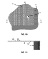
- FIG. 1B schematically shows a detail of fig. 1A .
- Figure 1B schematically shows a bar of the copper foil 12, the carbon film 16 and a large number of holes 18 in the carbon film. Over the carbon film and the holes a vitrified sample 22 in vitrified ice is provided.
- Figure 1C schematically shows a cross-section along line AA' of the detail shown in fig. 1B .
- Fig. 1C schematically shows a cross-section of a part of a copper bar 12, and carbon foil 16.
- Foil 16 shows a large number of holes 18.
- On top of the carbon film 16 a layer of vitrified ice 20 is shown, in which a sample 22 is present. An area of interest would thus be the part of the sample 22 that is located over a hole.
- the holes 18 are illuminated and the parts surrounding (bordering) the holes are not illuminated.
- the copper foil can also be another material, for example nickel, gold, (carbon coated) plastic, etc.
- the holes may show a thin layer of carbon, for example a layer of 3 nm. This is according to LARSON insufficient to absorb light or to provide an electrically conductive path from the sample to ground (the holder of the grid).
Landscapes
- Physics & Mathematics (AREA)
- General Physics & Mathematics (AREA)
- Chemical & Material Sciences (AREA)
- Analytical Chemistry (AREA)
- Health & Medical Sciences (AREA)
- Optics & Photonics (AREA)
- Biochemistry (AREA)
- General Health & Medical Sciences (AREA)
- Life Sciences & Earth Sciences (AREA)
- Immunology (AREA)
- Pathology (AREA)
- Nuclear Medicine, Radiotherapy & Molecular Imaging (AREA)
- Microscoopes, Condenser (AREA)
- Investigating, Analyzing Materials By Fluorescence Or Luminescence (AREA)
- Analysing Materials By The Use Of Radiation (AREA)
Abstract
Description
- The invention relates to a method of inspecting parts of a sample with a fluorescence microscope, at least part of the sample supported by a supporting film, the fluorescence microscope illuminating the sample with excitation light to generate fluorescence or phosphorescence, said sample vulnerable to damage by a temperature rise.
- Such a method is known from SCHWARTZ, Cindy L et al., 'Cryo-fluorescence microscopy facilitates correlations between light and cryo-electron microscopy and reduces the rate of photobleaching', J. Microsc. 2007 Aug 227(Pt 2), pp 98-109.
- The known method describes that in a setup for cryo-fluorescence microscopy a cryogenic vitrified sample is irradiated with light, and the fluorescence is observed.
- Cryogenic vitrified samples are, for example, biological samples that are frozen to arrest a sample in a given state. The formation of ice crystals during the freezing should be avoided as these crystals damage the structures of the sample, for example by puncturing cell membranes. Crystallization is avoided by freezing the sample to a temperature below the glass transition temperature of water of approximately 130 K at an ultra-high cooling rate, for example in the range of 105 K/s, or by cooling it by a combination of a high cooling rate and high pressure (103 K/s @ 2000 bar). These are techniques known per se, and described in e.g. US patent document
US 7,413,872 B2 and US patent documentUS 6,758,362 B2 , and (possibly after the use of for example a cryo-microtome) result in a sample with a typical thickness of 1 µm or less. - It is known that, when exposing the sample to light, the response of fluorescent markers to light diminishes over time. This is known as photo-bleaching. It is noted that the effect of photo-bleaching is less pronounced at cryogenic temperatures than at room temperature.
- After observing the sample with a light microscope and observing the fluorescence, the sample may be inspected in a Transmission Electron Microscope (TEM) for observing details with a resolution down to 10 nm or less. Therefore the samples are typically prepared on a TEM support grid. A TEM support grid is available from, for example, TED PELLA Inc., Redding, California, USA, see http://www.tedpella.com/supflm html/suptfilm.htm.
- A popular type of grid is the so-named holey carbon grid, in which a carbon support film is used, the carbon support film showing holes. Sample material suspended over the holes and embedded in ice can be inspected with for example transmitted electrons without interference (diffraction) of the carbon support film. It is noted that also holey carbon grids are known where the holes are not through-holes, but very thin carbon films of, for example, 3 nm or less.
- It is noted that it is known to make not a 2D image of the sample in the TEM, but a 3D tomogram. This is described in e.g. SARTORI, Anna et al., 'Correlative microscopy: Bridging the gap between fluorescence light microscopy and cryo-electron tomography', J. Struct. Biol. 160 (2007), p. 135-145. This results in a 3D image of the sample, instead of a 2D image.
- During fluorescence microscopy intense illumination is desired, such that the fluorescent signal can be collected in short time periods. This is advantageous in terms of signal-to-noise (the noise during a short period is less than the noise during a long period), but also to minimize specimen drift during detection. Also the ease of use is improved this way, quick availability of a high quality image is advantageous for searching and focusing onto an area of interest.
- A problem when using intense illumination is that heating may occur, damaging or destroying the specimen.
- The invention intends to provide a solution to heating when using intense illumination.
- To that end the method according to the invention is characterized in that
- the supporting film shows holes or thickness variations resulting in position dependent absorbance of the excitation light, resulting in parts with a high absorption of the excitation light and parts with a low absorption of the excitation light,
- the parts of the sample to be inspected are located over holes or parts of the supporting film with a low absorption of the excitation light; and
- the illumination is localized such that the parts of the supporting film with a high absorption of the excitation light and bordering the parts of the sample to be inspected are not illuminated.
- Obviously the heating is caused by absorption of the excitation light. The invention is based on the insight that the absorption of this light by a thin sample is often negligible, but that absorption by carbon is not. As an example: vitrified ice absorbs only very little light The heat that is generated in the carbon reaches the sample area by thermal conduction and in this way causes a temperature rise of the sample. The absorbance of thin carbon films is described in e.g. LARSON, D.M., et al. ,'The surface of evaporated carbon films is an insulating, high-bandgap material.', J. Struct. Biol. (2011).
- Absorbance is described in terms of optical density, in which the optical density A(λ) is defined as A(λ) = log10(I 0/I 1), with I 0 the amount of impinging light and I 1 the amount of transmitted light. LARSON shows in figure 2 that for a film thickness of more than 5 nm in close approximation A(λ) = [(D-5) x 0.016] nm-1 with D the thickness of the carbon film in nm. In other words: a layer of 11 nm of carbon already has an optical density A(λ) = 0.1 and thus absorbs 21% of the impinging light, and a layer of 65 nm absorbs approximately 90% of the impinging light (A(λ) = 1).
- A typical absorption figure of ice is of the order of 0.1 m-1 in the 300-600 nm domain, and -assuming there is an absorbing carbon layer- this is thus negligible compared to the absorption by a carbon layer.
- By using grids showing holes or thickness variations resulting in position dependent absorbance of the excitation light, and restricting inspection with intense illumination to areas of interest that are positioned over parts where the grid shows no or little absorbance, and avoiding illumination of the parts of the supporting film with a high absorption of the excitation light and bordering the parts of the sample to be inspected (positioned over the areas with low or no optical absorbance), dissipation due to intense illumination is avoided. As a result intense illumination can be used without damaging the sample.
- It is noted that these effects are very notable when studying vitrified cryogenic samples, where a temperature rise results in crystallization and/or sublimation and thus damage of the sample.
- It is noted that the person skilled in the art will understand that parts of the film far removed from the area of interest, that is: parts where heating (resulting in for example crystallization or sublimation) is allowed, may be illuminated by intense light, even if those parts show high absorbance. Also parts that are in directs contact with, for example, a copper mesh of the grid (or a material showing high thermal conductivity) may be illuminated without ice crystallization occurring.
- It is further noted that the whole sample may be exposed to a low light level, for example to determine where the borders between low and high absorbance are, as long as this does not result in a rise of temperature where damage occurs (for example such a temperature increase that ice crystallization occurs).
- Note that the temperature rise of a film not only depends on the absorbed light but also on the thermal conductivity of the film. Although a thinner film absorbs less light than a thick film, the thermal conduction of the thinner film also decreases and as a result the temperature rise can still be very high.
- Localization of the illumination can be achieved in several ways: by rastering a beam of light over the sample combined with intensity modulation of said beam, by vectoring the beam of light, or by illuminating the sample with a broad beam of light that passed through for example a spatial light modulator (SLM). An SLM is known per se and is used to vary the phase and/or amplitude of the transmitted light. An example of its use is, for example, in LCD projectors.
- It is noted that the use of a SLM in the optical illumination system of a FM is known and described in US patent no.
US 7,884,337 B2 . However, the SLM is here used to locally modulate the phase of the excitation light and does not vary the amount of impinging light on the sample (the intensity of light impinging on the sample). - It is important to realize that any other material that might be considered as a support film, as an alternative to carbon, is likely to have the same high absorbance as carbon. This is related to the wish to have a support film that is electrically conducting. Materials that are electrically conducting usually have a high optical absorbance.
- The combination of FM with TEM results in a powerful correlative microscopy, in which information of two different microscopy techniques are combined. The FM locates the areas with fluorescent markers (such as Green Fluorescent Protein [GFP] or an immuno-label), while TEM can be used for much higher resolution and locating heavy metal markers. Also FM can locate large structures and identify areas of interest to be inspected in the TEM at much higher magnification.
- Preferably the inspection is performed in an instrument comprising a FM mounted on the evacuable sample chamber of a TEM. Such instruments are commercially available as 'Tecnai with iCorr' from FEI Co., Hillsboro, USA.
- In an aspect of the invention an apparatus including a fluorescent microscope equipped with an illumination system to illuminate a vitrified sample with excitation light, and a detector for detecting fluorescent radiation emerging from the sample, is characterized in that the illumination system comprises a spatial light modulator for modulating the intensity of the excitation light, and the fluorescence microscope comprises a controller to control the spatial light modulator to localize the illumination.
- By equipping the illumination system of a fluorescence microscope with a spatial light modulator for modulating the intensity of the excitation light on the sample, and adding a controller for said spatial light modulator to the fluorescence microscope, the method described previously can be performed.
- Preferably this is combined with an electron microscope, even more preferably with a transmission electron microscope.
- The invention is now elucidated using figures, where identical reference numerals identify corresponding features. To that end:
-
Fig. 1A schematically shows a top view of a TEM grid; -
Fig. 1B schematically shows a detail ofFig. 1A ; and -
Fig. 1C schematically shows a cross-section of the detail shown in thefigure 1B . -
Fig. 1A schematically shows a top view of a TEM grid. - The
TEM grid 10 is a circularthin copper foil 12 with a thickness of approximately 25 µm and a diameter of 3.05 mm. The foil shows a large number of holes 14 (for example 400 per inch) and a thin film ofcarbon 16 on which a sample can be placed. The copper and carbon not only provide support, but also electrical conductivity to avoid charging. - It is noted that grids with a coarser or finer mesh are known, other materials (gold, nickel, (carbon coated) plastic), other forms of the holes (slots, hexagons), or forms differing from the thin circular foil (see e.g. US patent no.
US 7,767,979 andUS7,034,316 ). - It is further noted that the holes may show a thin layer of carbon, for example a layer of 3 nm. This is according to LARSON insufficient to absorb light or to provide an electrically conductive path from the sample to ground (the holder of the grid).
- The film need not be a carbon film, essential for the invention is that the film is an absorbing film, and that the absorption is avoided by not illuminating the parts of the foil where illumination leads to heat dissipation.
-
Fig. 1B schematically shows a detail offig. 1A , -
Figure 1B schematically shows a bar of thecopper foil 12, thecarbon film 16 and a large number ofholes 18 in the carbon film. Over the carbon film and the holes avitrified sample 22 in vitrified ice is provided. -
Figure 1C schematically shows a cross-section along line AA' of the detail shown infig. 1B . -
Fig. 1C schematically shows a cross-section of a part of acopper bar 12, andcarbon foil 16.Foil 16 shows a large number ofholes 18. On top of the carbon film 16 a layer ofvitrified ice 20 is shown, in which asample 22 is present. An area of interest would thus be the part of thesample 22 that is located over a hole. - When illuminating the grid with intense light, the
holes 18 are illuminated and the parts surrounding (bordering) the holes are not illuminated. - It is noted that the copper foil can also be another material, for example nickel, gold, (carbon coated) plastic, etc. It is further noted that the holes may show a thin layer of carbon, for example a layer of 3 nm. This is according to LARSON insufficient to absorb light or to provide an electrically conductive path from the sample to ground (the holder of the grid).
- It is further noted that, although the invention is only explained on the hand of a vitrified cryogenic sample, similar effects occur when studying, for example, chemical processes just below the temperature of a phase change, or when studying for example proteins.
- It is mentioned that localized illumination can be used in other applications as well, where illumination outside given boundaries, or avoiding certain areas, is demanded. We claim as follows:
-
- [-1-] SCHWARTZ, Cindy L. et al.; 'Cryo-fluorescence microscopy facilitates correlations between light and cryo-electron microscopy and reduces the rate of photobleaching', J. Microsc. 2007 Aug 227(Pt 2), pp 98-109.
- [-2-] Internet catalogue TED PELLA, Redding, California, USA, http://www.tedpella.com/supflm_html/suptfilm.htm, created Jan. 21th, 2013.
- [-3-] SARTORI, Anna et al., 'Correlative microscopy: Bridging the gap between fluorescence light microscopy and cryo-electron tomography', J. Struct. Biol. 160 (2007), p. 135-145.
- [-4-] LARSON, D.M. et al., 'The surface of evaporated carbon films is an insulating, high-bandgap material.', J. Struct. Biol. (2011).
Claims (15)
- Method of inspecting parts of a sample (22) with a fluorescence microscope, at least part of the sample supported by a supporting film (16), the fluorescence microscope illuminating the sample with excitation light to generate fluorescence or phosphorescence, said sample vulnerable to damage by a temperature rise,
characterized in that• the supporting film shows holes (18) or thickness variations resulting in position dependent absorbance of the excitation light, resulting in parts with a high absorption of the excitation light and parts with a low absorption of the excitation light,• the parts of the sample to be inspected are located over holes (18) or parts of the supporting film with a low absorption of the excitation light; and• the illumination with excitation light is a localized illumination, the localization such that the parts of the supporting film with a high absorption of the excitation light and bordering the parts of the sample to be inspected are not illuminated with excitation light. - The method of claim 1 in which the localization of the illumination is achieved by scanning a beam of excitation light over the sample and modulating the intensity of said beam.
- The method of claim 1 in which the localization of the illumination is achieved by vector scanning a beam of excitation light over the sample.
- The method of claim 1 in which the localization of the illumination is achieved by passing the excitation light through a spatial light modulator causing intensity modulation.
- The method of claim 4 in which the spatial light modulator is an LCD type spatial light modulator imaged on the sample.
- The method of any of the preceding claims in which the sample is a vitrified cryogenic sample.
- The method of any of the preceding claims in which the parts with a high absorption absorb more than 1 %, more specifically more than 10%, most specifically more than 90% of the excitation light, and the parts with a low absorption absorb less than 1 % of the excitation light.
- The method of claim 7 in which the parts with a high absorption comprise a layer with at least 5 nm of carbon, more specifically at least 11 nm of carbon, most specifically at least 65 nm of carbon, and the parts with a low absorption comprise a layer with at most 5 nm or no carbon layer at all.
- The method of any of the preceding claims in which prior to illuminating the sample to excite the sample while detecting fluorescence or phosphorescence, an image is taken with reflected or transmitted light to determine the borders of the supportive carbon film.
- The method of any of the preceding claims in which the method further involves imaging the sample in a transmission electron microscope.
- The method of claim 10 in which the transmission electron microscope is equipped with a sample chamber and the fluorescent image and the electron optical image are both acquired while the sample is on the sample chamber of the transmission electron microscope.
- Apparatus including a microscope equipped with an illumination system for illuminating a vitrified sample with excitation light, and a detector for detecting fluorescent radiation emerging from the sample,
characterized in that
the illumination system comprises a spatial light modulator for modulating the intensity of the excitation light, the fluorescent microscope comprises a controller to control the spatial light modulator to localize the illumination. - The apparatus of claim 12 in which the apparatus is equipped with means to keep a sample at a cryogenic temperature.
- The apparatus of claim 12 further including an electron microscope.
- The apparatus of claim 14 in which the electron microscope is a transmission electron microscope.
Priority Applications (4)
| Application Number | Priority Date | Filing Date | Title |
|---|---|---|---|
| EP13152215.3A EP2757402B1 (en) | 2013-01-22 | 2013-01-22 | Method of observing samples with a fluorescent microscope |
| JP2014007377A JP6262543B2 (en) | 2013-01-22 | 2014-01-20 | Sample observation method using a fluorescence microscope |
| US14/160,135 US20140203191A1 (en) | 2013-01-22 | 2014-01-21 | Method of Observing Samples with a Fluorescent Microscope |
| CN201410027787.0A CN103940791A (en) | 2013-01-22 | 2014-01-22 | Method of observing samples with a fluorescent microscope |
Applications Claiming Priority (1)
| Application Number | Priority Date | Filing Date | Title |
|---|---|---|---|
| EP13152215.3A EP2757402B1 (en) | 2013-01-22 | 2013-01-22 | Method of observing samples with a fluorescent microscope |
Publications (2)
| Publication Number | Publication Date |
|---|---|
| EP2757402A1 true EP2757402A1 (en) | 2014-07-23 |
| EP2757402B1 EP2757402B1 (en) | 2016-03-30 |
Family
ID=47715843
Family Applications (1)
| Application Number | Title | Priority Date | Filing Date |
|---|---|---|---|
| EP13152215.3A Active EP2757402B1 (en) | 2013-01-22 | 2013-01-22 | Method of observing samples with a fluorescent microscope |
Country Status (4)
| Country | Link |
|---|---|
| US (1) | US20140203191A1 (en) |
| EP (1) | EP2757402B1 (en) |
| JP (1) | JP6262543B2 (en) |
| CN (1) | CN103940791A (en) |
Families Citing this family (7)
| Publication number | Priority date | Publication date | Assignee | Title |
|---|---|---|---|---|
| EP2824445B1 (en) | 2013-07-08 | 2016-03-02 | Fei Company | Charged-particle microscopy combined with raman spectroscopy |
| SE537103C2 (en) | 2013-12-16 | 2015-01-07 | Per Fogelstrand | Fluorescence microscopy system and method with detection of light emission from multiple fluorochromes |
| US11101104B2 (en) * | 2019-08-30 | 2021-08-24 | Fei Company | Multi modal cryo compatible GUID grid |
| US12366509B2 (en) * | 2019-10-04 | 2025-07-22 | Mitegen, Llc | Sample supports and sample cooling systems for cryo-electron microscopy |
| CN111855567B (en) * | 2019-10-16 | 2021-07-20 | 中国科学院物理研究所 | A transmission electron microscope system and method for realizing optical intelligent focusing |
| WO2022256588A1 (en) * | 2021-06-04 | 2022-12-08 | Mitegen, Llc | Sample supports for cryo-electron microscopy |
| US20250076159A1 (en) * | 2023-08-28 | 2025-03-06 | Fei Company | Liquid specimen grid for transmission electron microscope |
Citations (8)
| Publication number | Priority date | Publication date | Assignee | Title |
|---|---|---|---|---|
| WO1999022262A1 (en) * | 1997-10-29 | 1999-05-06 | Macaulay Calum E | Apparatus and methods relating to spatially light modulated microscopy |
| US6758362B2 (en) | 1997-01-13 | 2004-07-06 | Leica Ag | Specimen holders for hydrous specimens and method of using them |
| US7034316B2 (en) | 2003-06-20 | 2006-04-25 | Fei Company | Sample carrier for carrying a sample to be irradiated with an electron beam |
| US20060226375A1 (en) * | 2005-04-06 | 2006-10-12 | Sharp Kabushiki Kaisha | Fluorescence detecting apparatus |
| US7413872B2 (en) | 2001-03-22 | 2008-08-19 | Universiteit Maastricht | Device for preparing specimens for a cryo-electron microscope |
| EP1998165A1 (en) * | 2007-06-01 | 2008-12-03 | The European Community, represented by the European Commission | Method of fluorescence imaging |
| US7767979B2 (en) | 2006-05-29 | 2010-08-03 | Fei Company | Method for coupling and disconnecting a co-operative composite structure of a sample carrier and a sample holder |
| US7884337B2 (en) | 2004-09-06 | 2011-02-08 | Hamamatsu Photonics K.K. | Fluorescent microscope and fluorescent correlation spectral analysis device |
Family Cites Families (5)
| Publication number | Priority date | Publication date | Assignee | Title |
|---|---|---|---|---|
| US6687035B2 (en) * | 2001-06-07 | 2004-02-03 | Leica Microsystems Heildelberg Gmbh | Method and apparatus for ROI-scan with high temporal resolution |
| ATE539345T1 (en) * | 2001-10-09 | 2012-01-15 | Univ Ruprecht Karls Heidelberg | MICROSCOPIC WIDE FIELD LIGHT METHOD |
| JP2005216645A (en) * | 2004-01-29 | 2005-08-11 | Jeol Ltd | Transmission electron microscope |
| US7355696B2 (en) * | 2005-02-01 | 2008-04-08 | Arryx, Inc | Method and apparatus for sorting cells |
| EP1953791A1 (en) * | 2007-02-05 | 2008-08-06 | FEI Company | Apparatus for observing a sample with a particle beam and an optical microscope |
-
2013
- 2013-01-22 EP EP13152215.3A patent/EP2757402B1/en active Active
-
2014
- 2014-01-20 JP JP2014007377A patent/JP6262543B2/en active Active
- 2014-01-21 US US14/160,135 patent/US20140203191A1/en not_active Abandoned
- 2014-01-22 CN CN201410027787.0A patent/CN103940791A/en active Pending
Patent Citations (8)
| Publication number | Priority date | Publication date | Assignee | Title |
|---|---|---|---|---|
| US6758362B2 (en) | 1997-01-13 | 2004-07-06 | Leica Ag | Specimen holders for hydrous specimens and method of using them |
| WO1999022262A1 (en) * | 1997-10-29 | 1999-05-06 | Macaulay Calum E | Apparatus and methods relating to spatially light modulated microscopy |
| US7413872B2 (en) | 2001-03-22 | 2008-08-19 | Universiteit Maastricht | Device for preparing specimens for a cryo-electron microscope |
| US7034316B2 (en) | 2003-06-20 | 2006-04-25 | Fei Company | Sample carrier for carrying a sample to be irradiated with an electron beam |
| US7884337B2 (en) | 2004-09-06 | 2011-02-08 | Hamamatsu Photonics K.K. | Fluorescent microscope and fluorescent correlation spectral analysis device |
| US20060226375A1 (en) * | 2005-04-06 | 2006-10-12 | Sharp Kabushiki Kaisha | Fluorescence detecting apparatus |
| US7767979B2 (en) | 2006-05-29 | 2010-08-03 | Fei Company | Method for coupling and disconnecting a co-operative composite structure of a sample carrier and a sample holder |
| EP1998165A1 (en) * | 2007-06-01 | 2008-12-03 | The European Community, represented by the European Commission | Method of fluorescence imaging |
Non-Patent Citations (6)
| Title |
|---|
| CINDI L. SCHWARTZ ET AL: "Cryo-fluorescence microscopy facilitates correlations between light and cryo-electron microscopy and reduces the rate of photobleaching", JOURNAL OF MICROSCOPY, vol. 227, no. 2, 1 August 2007 (2007-08-01), pages 98 - 109, XP055065629, ISSN: 0022-2720, DOI: 10.1111/j.1365-2818.2007.01794.x * |
| LARSON, D.M. ET AL.: "The surface of evaporated carbon films is an insulating, high-bandgap material.", J. STRUCT. BIOL., 2011 |
| SARTORI ET AL: "Correlative microscopy: Bridging the gap between fluorescence light microscopy and cryo-electron tomography", JOURNAL OF STRUCTURAL BIOLOGY, ACADEMIC PRESS, UNITED STATES, vol. 160, no. 2, 10 October 2007 (2007-10-10), pages 135 - 145, XP022346061, ISSN: 1047-8477, DOI: 10.1016/J.JSB.2007.07.011 * |
| SARTORI, ANNA ET AL.: "Correlative microscopy: Bridging the gap between fluorescence light microscopy and cryo-electron tomography", J. STRUCT. BIOL., vol. 160, 2007, pages 135 - 145 |
| SCHWARTZ, CINDY L ET AL.: "Cryo-fluorescence microscopy facilitates correlations between light and cryo-electron microscopy and reduces the rate of photobleaching", J. MICROSC., vol. 227, August 2007 (2007-08-01), pages 98 - 109, XP055065629, DOI: doi:10.1111/j.1365-2818.2007.01794.x |
| SCHWARTZ, CINDY L. ET AL.: "Cryo-fluorescence microscopy facilitates correlations between light and cryo-electron microscopy and reduces the rate of photobleaching", J. MICROSC., vol. 227, August 2007 (2007-08-01), pages 98 - 109, XP055065629, DOI: doi:10.1111/j.1365-2818.2007.01794.x |
Also Published As
| Publication number | Publication date |
|---|---|
| JP6262543B2 (en) | 2018-01-17 |
| EP2757402B1 (en) | 2016-03-30 |
| US20140203191A1 (en) | 2014-07-24 |
| CN103940791A (en) | 2014-07-23 |
| JP2014142639A (en) | 2014-08-07 |
Similar Documents
| Publication | Publication Date | Title |
|---|---|---|
| EP2757402B1 (en) | Method of observing samples with a fluorescent microscope | |
| JP6266119B2 (en) | Charged particle beam device, electron microscope, sample observation method | |
| Vila-Comamala et al. | Zone-doubled Fresnel zone plates for high-resolution hard X-ray full-field transmission microscopy | |
| Matsuyama et al. | Elemental mapping of frozen‐hydrated cells with cryo‐scanning X‐ray fluorescence microscopy | |
| JP7071825B2 (en) | Localization of nanopore fabrication on membranes by laser illumination during controlled failure | |
| Zachman et al. | Site-specific preparation of intact solid–liquid interfaces by label-free in situ localization and cryo-focused ion beam lift-out | |
| JP2016532267A (en) | Electron microscope sample support with porous metal foil | |
| KR100582627B1 (en) | Information acquisition device, section evaluation device and section evaluation method | |
| JP6112553B2 (en) | Observation system and observation method | |
| JP2006079846A (en) | Sample cross-section evaluation apparatus and sample cross-section evaluation method | |
| JP2006145526A (en) | Method for localizing fluorescent markers | |
| JP2014160068A5 (en) | ||
| Carlson et al. | Low-dose imaging techniques for transmission electron microscopy | |
| CN115997113A (en) | Method and apparatus for micromachining a sample using a focused ion beam | |
| US8674323B2 (en) | Forming an electron microscope sample from high-pressure frozen material | |
| US8306291B2 (en) | Method for localizing labels in a sample | |
| EP3885745B1 (en) | Single-crystal x-ray structure analysis apparatus and sample holder | |
| EP2881971A1 (en) | Method of producing a freestanding thin film of nano-crystalline graphite | |
| Dyck et al. | A versatile side entry laser system for scanning transmission electron microscopy | |
| EP2797100A1 (en) | Method of using a phase plate in a transmission electron microscope | |
| Gerasimova et al. | In situ focus characterization by ablation technique to enable optics alignment at an XUV FEL source | |
| JP6353646B2 (en) | Charged particle beam apparatus and sample observation method using the apparatus | |
| JP2005148003A (en) | Section processing apparatus and section evaluation method | |
| Radić et al. | Challenges of Electron Correlation Microscopy on Amorphous Silicon and Amorphous Germanium | |
| Winkler et al. | Multiplexed plasmonic nanoantennas for high throughput single molecule nanoscale dynamics in living cells |
Legal Events
| Date | Code | Title | Description |
|---|---|---|---|
| PUAI | Public reference made under article 153(3) epc to a published international application that has entered the european phase |
Free format text: ORIGINAL CODE: 0009012 |
|
| 17P | Request for examination filed |
Effective date: 20130122 |
|
| AK | Designated contracting states |
Kind code of ref document: A1 Designated state(s): AL AT BE BG CH CY CZ DE DK EE ES FI FR GB GR HR HU IE IS IT LI LT LU LV MC MK MT NL NO PL PT RO RS SE SI SK SM TR |
|
| AX | Request for extension of the european patent |
Extension state: BA ME |
|
| R17P | Request for examination filed (corrected) |
Effective date: 20150119 |
|
| RBV | Designated contracting states (corrected) |
Designated state(s): AL AT BE BG CH CY CZ DE DK EE ES FI FR GB GR HR HU IE IS IT LI LT LU LV MC MK MT NL NO PL PT RO RS SE SI SK SM TR |
|
| GRAP | Despatch of communication of intention to grant a patent |
Free format text: ORIGINAL CODE: EPIDOSNIGR1 |
|
| RIC1 | Information provided on ipc code assigned before grant |
Ipc: G01N 21/64 20060101ALI20151013BHEP Ipc: G02B 21/08 20060101AFI20151013BHEP Ipc: G02B 21/16 20060101ALI20151013BHEP |
|
| INTG | Intention to grant announced |
Effective date: 20151103 |
|
| GRAS | Grant fee paid |
Free format text: ORIGINAL CODE: EPIDOSNIGR3 |
|
| GRAA | (expected) grant |
Free format text: ORIGINAL CODE: 0009210 |
|
| AK | Designated contracting states |
Kind code of ref document: B1 Designated state(s): AL AT BE BG CH CY CZ DE DK EE ES FI FR GB GR HR HU IE IS IT LI LT LU LV MC MK MT NL NO PL PT RO RS SE SI SK SM TR |
|
| REG | Reference to a national code |
Ref country code: GB Ref legal event code: FG4D |
|
| REG | Reference to a national code |
Ref country code: CH Ref legal event code: EP |
|
| REG | Reference to a national code |
Ref country code: AT Ref legal event code: REF Ref document number: 785978 Country of ref document: AT Kind code of ref document: T Effective date: 20160415 |
|
| REG | Reference to a national code |
Ref country code: IE Ref legal event code: FG4D |
|
| REG | Reference to a national code |
Ref country code: DE Ref legal event code: R096 Ref document number: 602013005823 Country of ref document: DE |
|
| REG | Reference to a national code |
Ref country code: LT Ref legal event code: MG4D |
|
| PG25 | Lapsed in a contracting state [announced via postgrant information from national office to epo] |
Ref country code: FI Free format text: LAPSE BECAUSE OF FAILURE TO SUBMIT A TRANSLATION OF THE DESCRIPTION OR TO PAY THE FEE WITHIN THE PRESCRIBED TIME-LIMIT Effective date: 20160330 Ref country code: NO Free format text: LAPSE BECAUSE OF FAILURE TO SUBMIT A TRANSLATION OF THE DESCRIPTION OR TO PAY THE FEE WITHIN THE PRESCRIBED TIME-LIMIT Effective date: 20160630 Ref country code: GR Free format text: LAPSE BECAUSE OF FAILURE TO SUBMIT A TRANSLATION OF THE DESCRIPTION OR TO PAY THE FEE WITHIN THE PRESCRIBED TIME-LIMIT Effective date: 20160701 Ref country code: HR Free format text: LAPSE BECAUSE OF FAILURE TO SUBMIT A TRANSLATION OF THE DESCRIPTION OR TO PAY THE FEE WITHIN THE PRESCRIBED TIME-LIMIT Effective date: 20160330 |
|
| REG | Reference to a national code |
Ref country code: NL Ref legal event code: MP Effective date: 20160330 |
|
| REG | Reference to a national code |
Ref country code: AT Ref legal event code: MK05 Ref document number: 785978 Country of ref document: AT Kind code of ref document: T Effective date: 20160330 |
|
| PG25 | Lapsed in a contracting state [announced via postgrant information from national office to epo] |
Ref country code: LT Free format text: LAPSE BECAUSE OF FAILURE TO SUBMIT A TRANSLATION OF THE DESCRIPTION OR TO PAY THE FEE WITHIN THE PRESCRIBED TIME-LIMIT Effective date: 20160330 Ref country code: RS Free format text: LAPSE BECAUSE OF FAILURE TO SUBMIT A TRANSLATION OF THE DESCRIPTION OR TO PAY THE FEE WITHIN THE PRESCRIBED TIME-LIMIT Effective date: 20160330 Ref country code: SE Free format text: LAPSE BECAUSE OF FAILURE TO SUBMIT A TRANSLATION OF THE DESCRIPTION OR TO PAY THE FEE WITHIN THE PRESCRIBED TIME-LIMIT Effective date: 20160330 Ref country code: LV Free format text: LAPSE BECAUSE OF FAILURE TO SUBMIT A TRANSLATION OF THE DESCRIPTION OR TO PAY THE FEE WITHIN THE PRESCRIBED TIME-LIMIT Effective date: 20160330 |
|
| PG25 | Lapsed in a contracting state [announced via postgrant information from national office to epo] |
Ref country code: NL Free format text: LAPSE BECAUSE OF FAILURE TO SUBMIT A TRANSLATION OF THE DESCRIPTION OR TO PAY THE FEE WITHIN THE PRESCRIBED TIME-LIMIT Effective date: 20160330 |
|
| PG25 | Lapsed in a contracting state [announced via postgrant information from national office to epo] |
Ref country code: IS Free format text: LAPSE BECAUSE OF FAILURE TO SUBMIT A TRANSLATION OF THE DESCRIPTION OR TO PAY THE FEE WITHIN THE PRESCRIBED TIME-LIMIT Effective date: 20160730 Ref country code: EE Free format text: LAPSE BECAUSE OF FAILURE TO SUBMIT A TRANSLATION OF THE DESCRIPTION OR TO PAY THE FEE WITHIN THE PRESCRIBED TIME-LIMIT Effective date: 20160330 Ref country code: PL Free format text: LAPSE BECAUSE OF FAILURE TO SUBMIT A TRANSLATION OF THE DESCRIPTION OR TO PAY THE FEE WITHIN THE PRESCRIBED TIME-LIMIT Effective date: 20160330 |
|
| PG25 | Lapsed in a contracting state [announced via postgrant information from national office to epo] |
Ref country code: SK Free format text: LAPSE BECAUSE OF FAILURE TO SUBMIT A TRANSLATION OF THE DESCRIPTION OR TO PAY THE FEE WITHIN THE PRESCRIBED TIME-LIMIT Effective date: 20160330 Ref country code: PT Free format text: LAPSE BECAUSE OF FAILURE TO SUBMIT A TRANSLATION OF THE DESCRIPTION OR TO PAY THE FEE WITHIN THE PRESCRIBED TIME-LIMIT Effective date: 20160801 Ref country code: RO Free format text: LAPSE BECAUSE OF FAILURE TO SUBMIT A TRANSLATION OF THE DESCRIPTION OR TO PAY THE FEE WITHIN THE PRESCRIBED TIME-LIMIT Effective date: 20160330 Ref country code: AT Free format text: LAPSE BECAUSE OF FAILURE TO SUBMIT A TRANSLATION OF THE DESCRIPTION OR TO PAY THE FEE WITHIN THE PRESCRIBED TIME-LIMIT Effective date: 20160330 Ref country code: CZ Free format text: LAPSE BECAUSE OF FAILURE TO SUBMIT A TRANSLATION OF THE DESCRIPTION OR TO PAY THE FEE WITHIN THE PRESCRIBED TIME-LIMIT Effective date: 20160330 Ref country code: SM Free format text: LAPSE BECAUSE OF FAILURE TO SUBMIT A TRANSLATION OF THE DESCRIPTION OR TO PAY THE FEE WITHIN THE PRESCRIBED TIME-LIMIT Effective date: 20160330 Ref country code: ES Free format text: LAPSE BECAUSE OF FAILURE TO SUBMIT A TRANSLATION OF THE DESCRIPTION OR TO PAY THE FEE WITHIN THE PRESCRIBED TIME-LIMIT Effective date: 20160330 |
|
| PG25 | Lapsed in a contracting state [announced via postgrant information from national office to epo] |
Ref country code: BE Free format text: LAPSE BECAUSE OF FAILURE TO SUBMIT A TRANSLATION OF THE DESCRIPTION OR TO PAY THE FEE WITHIN THE PRESCRIBED TIME-LIMIT Effective date: 20160330 Ref country code: IT Free format text: LAPSE BECAUSE OF FAILURE TO SUBMIT A TRANSLATION OF THE DESCRIPTION OR TO PAY THE FEE WITHIN THE PRESCRIBED TIME-LIMIT Effective date: 20160330 |
|
| REG | Reference to a national code |
Ref country code: DE Ref legal event code: R097 Ref document number: 602013005823 Country of ref document: DE |
|
| REG | Reference to a national code |
Ref country code: FR Ref legal event code: PLFP Year of fee payment: 5 |
|
| PG25 | Lapsed in a contracting state [announced via postgrant information from national office to epo] |
Ref country code: DK Free format text: LAPSE BECAUSE OF FAILURE TO SUBMIT A TRANSLATION OF THE DESCRIPTION OR TO PAY THE FEE WITHIN THE PRESCRIBED TIME-LIMIT Effective date: 20160330 |
|
| PLBE | No opposition filed within time limit |
Free format text: ORIGINAL CODE: 0009261 |
|
| STAA | Information on the status of an ep patent application or granted ep patent |
Free format text: STATUS: NO OPPOSITION FILED WITHIN TIME LIMIT |
|
| 26N | No opposition filed |
Effective date: 20170103 |
|
| PG25 | Lapsed in a contracting state [announced via postgrant information from national office to epo] |
Ref country code: SI Free format text: LAPSE BECAUSE OF FAILURE TO SUBMIT A TRANSLATION OF THE DESCRIPTION OR TO PAY THE FEE WITHIN THE PRESCRIBED TIME-LIMIT Effective date: 20160330 |
|
| REG | Reference to a national code |
Ref country code: CH Ref legal event code: PL |
|
| PG25 | Lapsed in a contracting state [announced via postgrant information from national office to epo] |
Ref country code: MC Free format text: LAPSE BECAUSE OF FAILURE TO SUBMIT A TRANSLATION OF THE DESCRIPTION OR TO PAY THE FEE WITHIN THE PRESCRIBED TIME-LIMIT Effective date: 20160330 |
|
| PG25 | Lapsed in a contracting state [announced via postgrant information from national office to epo] |
Ref country code: LI Free format text: LAPSE BECAUSE OF NON-PAYMENT OF DUE FEES Effective date: 20170131 Ref country code: CH Free format text: LAPSE BECAUSE OF NON-PAYMENT OF DUE FEES Effective date: 20170131 |
|
| REG | Reference to a national code |
Ref country code: IE Ref legal event code: MM4A |
|
| PG25 | Lapsed in a contracting state [announced via postgrant information from national office to epo] |
Ref country code: LU Free format text: LAPSE BECAUSE OF NON-PAYMENT OF DUE FEES Effective date: 20170122 |
|
| REG | Reference to a national code |
Ref country code: FR Ref legal event code: PLFP Year of fee payment: 6 |
|
| PG25 | Lapsed in a contracting state [announced via postgrant information from national office to epo] |
Ref country code: IE Free format text: LAPSE BECAUSE OF NON-PAYMENT OF DUE FEES Effective date: 20170122 |
|
| PG25 | Lapsed in a contracting state [announced via postgrant information from national office to epo] |
Ref country code: MT Free format text: LAPSE BECAUSE OF NON-PAYMENT OF DUE FEES Effective date: 20170122 |
|
| PG25 | Lapsed in a contracting state [announced via postgrant information from national office to epo] |
Ref country code: AL Free format text: LAPSE BECAUSE OF FAILURE TO SUBMIT A TRANSLATION OF THE DESCRIPTION OR TO PAY THE FEE WITHIN THE PRESCRIBED TIME-LIMIT Effective date: 20160330 |
|
| PG25 | Lapsed in a contracting state [announced via postgrant information from national office to epo] |
Ref country code: HU Free format text: LAPSE BECAUSE OF FAILURE TO SUBMIT A TRANSLATION OF THE DESCRIPTION OR TO PAY THE FEE WITHIN THE PRESCRIBED TIME-LIMIT; INVALID AB INITIO Effective date: 20130122 |
|
| PG25 | Lapsed in a contracting state [announced via postgrant information from national office to epo] |
Ref country code: BG Free format text: LAPSE BECAUSE OF FAILURE TO SUBMIT A TRANSLATION OF THE DESCRIPTION OR TO PAY THE FEE WITHIN THE PRESCRIBED TIME-LIMIT Effective date: 20160330 |
|
| PG25 | Lapsed in a contracting state [announced via postgrant information from national office to epo] |
Ref country code: CY Free format text: LAPSE BECAUSE OF NON-PAYMENT OF DUE FEES Effective date: 20160330 |
|
| PG25 | Lapsed in a contracting state [announced via postgrant information from national office to epo] |
Ref country code: MK Free format text: LAPSE BECAUSE OF FAILURE TO SUBMIT A TRANSLATION OF THE DESCRIPTION OR TO PAY THE FEE WITHIN THE PRESCRIBED TIME-LIMIT Effective date: 20160330 |
|
| PG25 | Lapsed in a contracting state [announced via postgrant information from national office to epo] |
Ref country code: TR Free format text: LAPSE BECAUSE OF FAILURE TO SUBMIT A TRANSLATION OF THE DESCRIPTION OR TO PAY THE FEE WITHIN THE PRESCRIBED TIME-LIMIT Effective date: 20160330 |
|
| PGFP | Annual fee paid to national office [announced via postgrant information from national office to epo] |
Ref country code: GB Payment date: 20260108 Year of fee payment: 14 |
|
| PGFP | Annual fee paid to national office [announced via postgrant information from national office to epo] |
Ref country code: DE Payment date: 20251211 Year of fee payment: 14 |
|
| PGFP | Annual fee paid to national office [announced via postgrant information from national office to epo] |
Ref country code: FR Payment date: 20260114 Year of fee payment: 14 |