EP2755235A1 - Solid-state image pickup element and solid-state image pickup element mounting structure - Google Patents
Solid-state image pickup element and solid-state image pickup element mounting structure Download PDFInfo
- Publication number
- EP2755235A1 EP2755235A1 EP12830624.8A EP12830624A EP2755235A1 EP 2755235 A1 EP2755235 A1 EP 2755235A1 EP 12830624 A EP12830624 A EP 12830624A EP 2755235 A1 EP2755235 A1 EP 2755235A1
- Authority
- EP
- European Patent Office
- Prior art keywords
- electrode pads
- image pickup
- solid
- state image
- pickup element
- Prior art date
- Legal status (The legal status is an assumption and is not a legal conclusion. Google has not performed a legal analysis and makes no representation as to the accuracy of the status listed.)
- Granted
Links
Images






Classifications
-
- H—ELECTRICITY
- H10—SEMICONDUCTOR DEVICES; ELECTRIC SOLID-STATE DEVICES NOT OTHERWISE PROVIDED FOR
- H10F—INORGANIC SEMICONDUCTOR DEVICES SENSITIVE TO INFRARED RADIATION, LIGHT, ELECTROMAGNETIC RADIATION OF SHORTER WAVELENGTH OR CORPUSCULAR RADIATION
- H10F99/00—Subject matter not provided for in other groups of this subclass
-
- H—ELECTRICITY
- H10—SEMICONDUCTOR DEVICES; ELECTRIC SOLID-STATE DEVICES NOT OTHERWISE PROVIDED FOR
- H10F—INORGANIC SEMICONDUCTOR DEVICES SENSITIVE TO INFRARED RADIATION, LIGHT, ELECTROMAGNETIC RADIATION OF SHORTER WAVELENGTH OR CORPUSCULAR RADIATION
- H10F39/00—Integrated devices, or assemblies of multiple devices, comprising at least one element covered by group H10F30/00, e.g. radiation detectors comprising photodiode arrays
- H10F39/80—Constructional details of image sensors
- H10F39/804—Containers or encapsulations
-
- H—ELECTRICITY
- H10—SEMICONDUCTOR DEVICES; ELECTRIC SOLID-STATE DEVICES NOT OTHERWISE PROVIDED FOR
- H10F—INORGANIC SEMICONDUCTOR DEVICES SENSITIVE TO INFRARED RADIATION, LIGHT, ELECTROMAGNETIC RADIATION OF SHORTER WAVELENGTH OR CORPUSCULAR RADIATION
- H10F39/00—Integrated devices, or assemblies of multiple devices, comprising at least one element covered by group H10F30/00, e.g. radiation detectors comprising photodiode arrays
- H10F39/80—Constructional details of image sensors
- H10F39/811—Interconnections
-
- H—ELECTRICITY
- H10—SEMICONDUCTOR DEVICES; ELECTRIC SOLID-STATE DEVICES NOT OTHERWISE PROVIDED FOR
- H10F—INORGANIC SEMICONDUCTOR DEVICES SENSITIVE TO INFRARED RADIATION, LIGHT, ELECTROMAGNETIC RADIATION OF SHORTER WAVELENGTH OR CORPUSCULAR RADIATION
- H10F39/00—Integrated devices, or assemblies of multiple devices, comprising at least one element covered by group H10F30/00, e.g. radiation detectors comprising photodiode arrays
- H10F39/10—Integrated devices
- H10F39/12—Image sensors
-
- H—ELECTRICITY
- H10—SEMICONDUCTOR DEVICES; ELECTRIC SOLID-STATE DEVICES NOT OTHERWISE PROVIDED FOR
- H10W—GENERIC PACKAGES, INTERCONNECTIONS, CONNECTORS OR OTHER CONSTRUCTIONAL DETAILS OF DEVICES COVERED BY CLASS H10
- H10W70/00—Package substrates; Interposers; Redistribution layers [RDL]
- H10W70/60—Insulating or insulated package substrates; Interposers; Redistribution layers
- H10W70/62—Insulating or insulated package substrates; Interposers; Redistribution layers characterised by their interconnections
- H10W70/63—Vias, e.g. via plugs
-
- H—ELECTRICITY
- H10—SEMICONDUCTOR DEVICES; ELECTRIC SOLID-STATE DEVICES NOT OTHERWISE PROVIDED FOR
- H10W—GENERIC PACKAGES, INTERCONNECTIONS, CONNECTORS OR OTHER CONSTRUCTIONAL DETAILS OF DEVICES COVERED BY CLASS H10
- H10W70/00—Package substrates; Interposers; Redistribution layers [RDL]
- H10W70/60—Insulating or insulated package substrates; Interposers; Redistribution layers
- H10W70/62—Insulating or insulated package substrates; Interposers; Redistribution layers characterised by their interconnections
- H10W70/65—Shapes or dispositions of interconnections
-
- H—ELECTRICITY
- H10—SEMICONDUCTOR DEVICES; ELECTRIC SOLID-STATE DEVICES NOT OTHERWISE PROVIDED FOR
- H10W—GENERIC PACKAGES, INTERCONNECTIONS, CONNECTORS OR OTHER CONSTRUCTIONAL DETAILS OF DEVICES COVERED BY CLASS H10
- H10W70/00—Package substrates; Interposers; Redistribution layers [RDL]
- H10W70/60—Insulating or insulated package substrates; Interposers; Redistribution layers
- H10W70/62—Insulating or insulated package substrates; Interposers; Redistribution layers characterised by their interconnections
- H10W70/65—Shapes or dispositions of interconnections
- H10W70/654—Top-view layouts
-
- H—ELECTRICITY
- H10—SEMICONDUCTOR DEVICES; ELECTRIC SOLID-STATE DEVICES NOT OTHERWISE PROVIDED FOR
- H10W—GENERIC PACKAGES, INTERCONNECTIONS, CONNECTORS OR OTHER CONSTRUCTIONAL DETAILS OF DEVICES COVERED BY CLASS H10
- H10W70/00—Package substrates; Interposers; Redistribution layers [RDL]
- H10W70/60—Insulating or insulated package substrates; Interposers; Redistribution layers
- H10W70/67—Insulating or insulated package substrates; Interposers; Redistribution layers characterised by their insulating layers or insulating parts
- H10W70/68—Shapes or dispositions thereof
- H10W70/681—Shapes or dispositions thereof comprising holes not having chips therein, e.g. for outgassing, underfilling or bond wire passage
-
- H—ELECTRICITY
- H10—SEMICONDUCTOR DEVICES; ELECTRIC SOLID-STATE DEVICES NOT OTHERWISE PROVIDED FOR
- H10W—GENERIC PACKAGES, INTERCONNECTIONS, CONNECTORS OR OTHER CONSTRUCTIONAL DETAILS OF DEVICES COVERED BY CLASS H10
- H10W72/00—Interconnections or connectors in packages
- H10W72/20—Bump connectors, e.g. solder bumps or copper pillars; Dummy bumps; Thermal bumps
- H10W72/29—Bond pads specially adapted therefor
-
- H—ELECTRICITY
- H10—SEMICONDUCTOR DEVICES; ELECTRIC SOLID-STATE DEVICES NOT OTHERWISE PROVIDED FOR
- H10W—GENERIC PACKAGES, INTERCONNECTIONS, CONNECTORS OR OTHER CONSTRUCTIONAL DETAILS OF DEVICES COVERED BY CLASS H10
- H10W72/00—Interconnections or connectors in packages
- H10W72/50—Bond wires
- H10W72/541—Dispositions of bond wires
- H10W72/5445—Dispositions of bond wires being orthogonal to a side surface of the chip, e.g. parallel arrangements
-
- H—ELECTRICITY
- H10—SEMICONDUCTOR DEVICES; ELECTRIC SOLID-STATE DEVICES NOT OTHERWISE PROVIDED FOR
- H10W—GENERIC PACKAGES, INTERCONNECTIONS, CONNECTORS OR OTHER CONSTRUCTIONAL DETAILS OF DEVICES COVERED BY CLASS H10
- H10W72/00—Interconnections or connectors in packages
- H10W72/50—Bond wires
- H10W72/59—Bond pads specially adapted therefor
-
- H—ELECTRICITY
- H10—SEMICONDUCTOR DEVICES; ELECTRIC SOLID-STATE DEVICES NOT OTHERWISE PROVIDED FOR
- H10W—GENERIC PACKAGES, INTERCONNECTIONS, CONNECTORS OR OTHER CONSTRUCTIONAL DETAILS OF DEVICES COVERED BY CLASS H10
- H10W72/00—Interconnections or connectors in packages
- H10W72/851—Dispositions of multiple connectors or interconnections
- H10W72/874—On different surfaces
- H10W72/884—Die-attach connectors and bond wires
-
- H—ELECTRICITY
- H10—SEMICONDUCTOR DEVICES; ELECTRIC SOLID-STATE DEVICES NOT OTHERWISE PROVIDED FOR
- H10W—GENERIC PACKAGES, INTERCONNECTIONS, CONNECTORS OR OTHER CONSTRUCTIONAL DETAILS OF DEVICES COVERED BY CLASS H10
- H10W72/00—Interconnections or connectors in packages
- H10W72/90—Bond pads, in general
-
- H—ELECTRICITY
- H10—SEMICONDUCTOR DEVICES; ELECTRIC SOLID-STATE DEVICES NOT OTHERWISE PROVIDED FOR
- H10W—GENERIC PACKAGES, INTERCONNECTIONS, CONNECTORS OR OTHER CONSTRUCTIONAL DETAILS OF DEVICES COVERED BY CLASS H10
- H10W72/00—Interconnections or connectors in packages
- H10W72/90—Bond pads, in general
- H10W72/921—Structures or relative sizes of bond pads
- H10W72/922—Bond pads being integral with underlying chip-level interconnections
-
- H—ELECTRICITY
- H10—SEMICONDUCTOR DEVICES; ELECTRIC SOLID-STATE DEVICES NOT OTHERWISE PROVIDED FOR
- H10W—GENERIC PACKAGES, INTERCONNECTIONS, CONNECTORS OR OTHER CONSTRUCTIONAL DETAILS OF DEVICES COVERED BY CLASS H10
- H10W72/00—Interconnections or connectors in packages
- H10W72/90—Bond pads, in general
- H10W72/921—Structures or relative sizes of bond pads
- H10W72/926—Multiple bond pads having different sizes
-
- H—ELECTRICITY
- H10—SEMICONDUCTOR DEVICES; ELECTRIC SOLID-STATE DEVICES NOT OTHERWISE PROVIDED FOR
- H10W—GENERIC PACKAGES, INTERCONNECTIONS, CONNECTORS OR OTHER CONSTRUCTIONAL DETAILS OF DEVICES COVERED BY CLASS H10
- H10W72/00—Interconnections or connectors in packages
- H10W72/90—Bond pads, in general
- H10W72/931—Shapes of bond pads
- H10W72/932—Plan-view shape, i.e. in top view
-
- H—ELECTRICITY
- H10—SEMICONDUCTOR DEVICES; ELECTRIC SOLID-STATE DEVICES NOT OTHERWISE PROVIDED FOR
- H10W—GENERIC PACKAGES, INTERCONNECTIONS, CONNECTORS OR OTHER CONSTRUCTIONAL DETAILS OF DEVICES COVERED BY CLASS H10
- H10W72/00—Interconnections or connectors in packages
- H10W72/90—Bond pads, in general
- H10W72/931—Shapes of bond pads
- H10W72/936—Multiple bond pads having different shapes
-
- H—ELECTRICITY
- H10—SEMICONDUCTOR DEVICES; ELECTRIC SOLID-STATE DEVICES NOT OTHERWISE PROVIDED FOR
- H10W—GENERIC PACKAGES, INTERCONNECTIONS, CONNECTORS OR OTHER CONSTRUCTIONAL DETAILS OF DEVICES COVERED BY CLASS H10
- H10W72/00—Interconnections or connectors in packages
- H10W72/90—Bond pads, in general
- H10W72/941—Dispositions of bond pads
- H10W72/944—Dispositions of multiple bond pads
- H10W72/9445—Top-view layouts, e.g. mirror arrays
-
- H—ELECTRICITY
- H10—SEMICONDUCTOR DEVICES; ELECTRIC SOLID-STATE DEVICES NOT OTHERWISE PROVIDED FOR
- H10W—GENERIC PACKAGES, INTERCONNECTIONS, CONNECTORS OR OTHER CONSTRUCTIONAL DETAILS OF DEVICES COVERED BY CLASS H10
- H10W74/00—Encapsulations, e.g. protective coatings
- H10W74/10—Encapsulations, e.g. protective coatings characterised by their shape or disposition
- H10W74/15—Encapsulations, e.g. protective coatings characterised by their shape or disposition on active surfaces of flip-chip devices, e.g. underfills
-
- H—ELECTRICITY
- H10—SEMICONDUCTOR DEVICES; ELECTRIC SOLID-STATE DEVICES NOT OTHERWISE PROVIDED FOR
- H10W—GENERIC PACKAGES, INTERCONNECTIONS, CONNECTORS OR OTHER CONSTRUCTIONAL DETAILS OF DEVICES COVERED BY CLASS H10
- H10W90/00—Package configurations
- H10W90/701—Package configurations characterised by the relative positions of pads or connectors relative to package parts
- H10W90/721—Package configurations characterised by the relative positions of pads or connectors relative to package parts of bump connectors
- H10W90/724—Package configurations characterised by the relative positions of pads or connectors relative to package parts of bump connectors between a chip and a stacked insulating package substrate, interposer or RDL
-
- H—ELECTRICITY
- H10—SEMICONDUCTOR DEVICES; ELECTRIC SOLID-STATE DEVICES NOT OTHERWISE PROVIDED FOR
- H10W—GENERIC PACKAGES, INTERCONNECTIONS, CONNECTORS OR OTHER CONSTRUCTIONAL DETAILS OF DEVICES COVERED BY CLASS H10
- H10W90/00—Package configurations
- H10W90/701—Package configurations characterised by the relative positions of pads or connectors relative to package parts
- H10W90/731—Package configurations characterised by the relative positions of pads or connectors relative to package parts of die-attach connectors
- H10W90/734—Package configurations characterised by the relative positions of pads or connectors relative to package parts of die-attach connectors between a chip and a stacked insulating package substrate, interposer or RDL
-
- H—ELECTRICITY
- H10—SEMICONDUCTOR DEVICES; ELECTRIC SOLID-STATE DEVICES NOT OTHERWISE PROVIDED FOR
- H10W—GENERIC PACKAGES, INTERCONNECTIONS, CONNECTORS OR OTHER CONSTRUCTIONAL DETAILS OF DEVICES COVERED BY CLASS H10
- H10W90/00—Package configurations
- H10W90/701—Package configurations characterised by the relative positions of pads or connectors relative to package parts
- H10W90/751—Package configurations characterised by the relative positions of pads or connectors relative to package parts of bond wires
- H10W90/754—Package configurations characterised by the relative positions of pads or connectors relative to package parts of bond wires between a chip and a stacked insulating package substrate, interposer or RDL
Definitions
- the present invention relates to a solid-state image pickup element and a solid-state image pickup element mounting structure.
- a known solid-state image pickup element is a so-called front-illuminated solid-state image pickup element provided with a semiconductor substrate having a sensitive region, and a plurality of electrode pads arrayed on a principal face of the semiconductor substrate, wherein the principal face side of the semiconductor substrate is a light receiving surface side (e.g., cf. Patent Literature 1).
- Another known solid-state image pickup element is a so-called back-illuminated solid-state image pickup element provided with a semiconductor substrate having a sensitive region, and a plurality of electrode pads arrayed on a principal face of the semiconductor substrate, wherein the back face side to the principal face of the semiconductor substrate is a light receiving surface side (e.g., cf. Patent Literature 2).
- Patent Literature 1 Japanese Patent Application Laid-Open Publication No. H10-107255
- a surface of the former to be opposed to a mounting member (e.g., a wiring substrate or the like) on which the solid-state image pickup element is to be mounted is reverse to that of the latter and an arrangement of the electrode pads arrayed on the principal face of the semiconductor substrate in the former is also reverse to that in the latter.
- a mounting member e.g., a wiring substrate or the like
- an arrangement of the electrode pads arrayed on the principal face of the semiconductor substrate in the former is also reverse to that in the latter.
- An aspect of the present invention is a solid-state image pickup element comprising: a semiconductor substrate having a photosensitive region; a plurality of first electrode pads arrayed on a principal face of the semiconductor substrate; a plurality of second electrode pads arrayed in a direction along a direction in which the plurality of first electrode pads are arrayed, on the principal face of the semiconductor substrate; and a plurality of interconnections connecting the plurality of first electrode pads and the plurality of second electrode pads in one-to-one correspondence, wherein the plurality of interconnections connect the first and second electrode pads so that each interconnection connects the first electrode pad and the second electrode pad in a positional relation of line symmetry with respect to a center line perpendicular to the array directions of the plurality of first and second electrode pads.
- the first electrode pad and the second electrode pad in the positional relation of line symmetry with respect to the center line perpendicular to the array directions of the plurality of first and second electrode pads are connected through the interconnection. Therefore, even with reversal of the principal face and the back face to this principal face, the positions of the first electrode pad and the second electrode pad connected to each other through the interconnection are the same in the array directions of the respective electrode pads.
- the plurality of first electrode pads may be located nearer to an edge of the semiconductor substrate than the plurality of second electrode pads are. In this case, the connection by wire bonding to each first electrode pad becomes easier when the solid-state image pickup element is mounted on the mounting member with the back face to the principal face being opposite thereto.
- Another aspect of the present invention is a solid-state image pickup element comprising: a semiconductor substrate of a rectangular shape having a photosensitive region; a plurality of first electrode pads arrayed in a first direction along one side of the semiconductor substrate, on a principal face of the semiconductor substrate; a plurality of second electrode pads arrayed in the first direction on the principal face of the semiconductor substrate; and a plurality of interconnections connecting the plurality of first electrode pads and the plurality of second electrode pads in one-to-one correspondence, wherein the plurality of interconnections connect the first and second electrode pads so that each interconnection connects the first electrode pad and the second electrode pad in an identical order relation in an array order in the first direction among the plurality of first electrode pads and in an array order in a second direction opposite to the first direction among the plurality of second electrode pads.
- the first electrode pad and the second electrode pad in the same order relation in the array order in the first direction among the plurality of first electrode pads and in the array order in the second direction among the plurality of second electrode pads are connected through the interconnection. Therefore, even with reversal of the principal face of the semiconductor substrate and the back face to this principal face, the positions of the first electrode pad and the second electrode pad connected to each other through the interconnection are the same in the array orders of the respective electrode pads.
- the plurality of first electrode pads may be located nearer to the aforementioned one side of the semiconductor substrate than the plurality of second electrode pads are. In this case, the connection by wire bonding to each first electrode pad becomes easier when the solid-state image pickup element is mounted on the mounting member with the back face to the principal face being opposite thereto.
- the semiconductor substrate may have a light receiving surface side defined on the principal face side and the semiconductor substrate may have a light receiving surface side defined on the the back face side to the principal face.
- the principal face side is the light receiving surface side
- the front-illuminated solid-state image pickup element is realized.
- the back face side to the principal face is the light receiving surface side
- the back-illuminated solid-state image pickup element is realized.
- Still another aspect of the present invention is a solid-state image pickup element mounting structure comprising: the aforementioned solid-state image pickup element; and a mounting member on which the solid-state image pickup element is mounted and in which a plurality of third electrode pads are arranged on a principal face thereof, wherein the solid-state image pickup element is mounted on the mounting member so that the back face to the principal face of the solid-state image pickup element is opposite to the principal face of the mounting member, and wherein the plurality of first electrode pads and the plurality of third electrode pads are connected by wire bonding.
- Another aspect of the present invention is a solid-state image pickup element mounting structure comprising: the foregoing solid-state image pickup element; and a mounting member on which the solid-state image pickup element is mounted and in which a plurality of third electrode pads are arranged on a principal face thereof, wherein the solid-state image pickup element is mounted on the mounting member so that the principal face of the solid-state image pickup element is opposite to the principal face of the mounting member, and wherein the plurality of second electrode pads and the plurality of third electrode pads are connected by flip chip bonding.
- Another aspect of the present invention is a solid-state image pickup element mounting structure comprising: the foregoing solid-state image pickup element; and a mounting member on which the solid-state image pickup element is mounted and in which a plurality of third electrode pads are arranged on a principal face thereof, wherein the solid-state image pickup element is mounted on the mounting member so that the principal face of the solid-state image pickup element is opposite to a back face to the principal face of the mounting member, and wherein the plurality of second electrode pads and the plurality of third electrode pads are connected by wire bonding.
- the present invention allows easy reduction of the cost and preparatory period of the external circuit or the mounting member or the like.
- the present invention provides the solid-state image pickup elements and the solid-state image pickup element mounting structures allowing easy reduction of the cost and preparatory period of the external circuit or the mounting member or the like.
- Fig. 1 is a plan view showing the front-illuminated solid-state image pickup element according to the present embodiment.
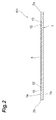
- Fig. 2 is a drawing illustrating a cross-sectional configuration of the front-illuminated solid-state image pickup element according to the present embodiment.
- the front-illuminated solid-state image pickup element IS 1 is provided with a semiconductor substrate 1, a plurality of first electrode pads 10, a plurality of second electrode pads 12, and a plurality of interconnections 14.
- the solid-state image pickup element IS1 is a so-called FI (Front-Illuminated)-CCD image sensor.
- the illustration of the interconnections 14 is omitted from Fig. 2 .
- the semiconductor substrate 1 has a rectangular shape on the plane view and has four sides 2a-2d constituting the edge of the semiconductor substrate 1.
- the semiconductor substrate 1 includes principal faces 1a, 1b opposed to each other.
- the semiconductor substrate 1 has a photosensitive region (image pickup region) 3 formed on the principal face 1a side.
- a CCD for image pickup consisting of a plurality of vertical shift registers (not shown) is formed as pixels.
- the principal face 1a side is a light receiving surface side.
- Fig. 1 is the plan view of the solid-state image pickup element IS1 as viewed from the light receiving surface (principal face 1a) side.
- a light image incident on the photosensitive region 3 is converted into a two-dimensional electric charge image and electric charges are transferred along the vertical direction by the vertical shift registers.
- a horizontal shift register (not shown) is provided at an end in the charge transfer direction of the photosensitive region 3. The electric charges of the respective pixels having been transferred in the vertical direction are sequentially transferred along the horizontal direction by the horizontal shift register.
- the charge transfer method of the CCD may be a known method such as the frame transfer method, the interline transfer method, or the full frame transfer method.
- Each first electrode pad 10 is arranged on the principal face 1a of the semiconductor substrate 1.
- Each first electrode pad 10 is provided in one of regions near to the two opposed sides 2a, 2b with the photosensitive region 3 in between the first electrode pads 10.
- twelve first electrode pads 10 are provided in each of the regions near to the respective sides 2a, 2b.
- the first electrode pads 10 each are arrayed in a direction along the sides 2a, 2b of the semiconductor substrate 1.
- the first electrode pads 10 have a rectangular shape.
- Each second electrode pad 12 is also arranged on the principal face 1a of the semiconductor substrate 1.
- Each second electrode pad 12 is provided in one of the regions near to the foregoing two sides 2a, 2b and they are arrayed in the direction along the sides 2a, 2b of the semiconductor substrate 1 as the first electrode pads 10 are.
- twelve second electrode pads 12 are provided in each of the regions near to the respective sides 2a, 2b. Namely, there are twenty four second electrode pads 12 provided.
- the second electrode pads 12 have a circular shape.
- the first electrode pads 10 are located nearer to the edge of the semiconductor substrate 1 or nearer to the sides 2a, 2b than the second electrode pads 12 are.
- the first electrode pads 10 and the second electrode pads 12 are arranged in zigzag patterns.
- the first electrode pads 10 and the second electrode pads 12 each include electrode pads for applying a transfer voltage to charge transfer electrodes for transferring electric charges in the vertical direction, an electrode pad for applying a transfer voltage to a charge transfer electrode for transferring electric charges in the horizontal direction, an electrode pad for reading out the electric charges having been transferred in the horizontal direction, an electrode pad for extracting outputs, an electrode pad for execution of a test operation, and so on.
- Each interconnection 14, as shown in Fig. 1 is provided on the semiconductor substrate 1 and connects the first electrode pad 10 and the second electrode pad 12 in one-to-one correspondence.
- Each interconnection 14 connects the first electrode pad 10 and the second electrode pad 12 in a positional relation of line symmetry with respect to a center line l perpendicular to the array directions of the first and second electrode pads 10, 12.
- each interconnection 14 connects the first electrode pad 10 and the second electrode pad 12 in an identical order relation in an array order in a first direction (e.g., a direction from the side 2c to the side 2d) along the side 2a (or the side 2b) among the first electrode pads 10 and in an array order in a second direction (e.g., a direction from the side 2d to the side 2c) opposite to the first direction.
- a first direction e.g., a direction from the side 2c to the side 2d
- a second direction e.g., a direction from the side 2d to the side 2c
- Fig. 3 is a plan view showing the back-illuminated solid-state image pickup element according to the present embodiment.
- Fig. 4 is a drawing illustrating a cross-sectional view of the back-illuminated solid-state image pickup element according to the present embodiment. The illustration of the interconnections 14 is omitted from Fig. 4 .
- the back-illuminated solid-state image pickup element IS2 is provided with the semiconductor substrate 1, the plurality of first electrode pads 10, the plurality of second electrode pads 12, and the plurality of interconnections 14 as the solid-state image pickup element IS1 is.
- the solid-state image pickup element IS2 is a so-called BT (Back-Thinned)-CCD image sensor.
- the semiconductor substrate 1 is thinned by etching a central region thereof with an aqueous KOH solution from the principal face 1b side. This thinning results in forming a recess portion on the principal face 1b side in the central region of the semiconductor substrate 1.
- a frame portion thicker than the recess portion is present around the recess portion of the semiconductor substrate 1.
- the frame portion may be removed by etching whereby the solid-state image pickup element IS2 is constructed as a BT-CCD image sensor wherein the entire region of the semiconductor substrate 1 is thinned.
- Fig. 3 is the plan view of the solid-state image pickup element IS2 as viewed from the back face (principal face 1a) side to the light receiving surface.
- Fig. 3 like Fig. 1 , is drawn without the illustration of interconnections electrically connecting the photosensitive region 3 and each of the electrode pads 10, 12.
- each interconnection 14 connects the first electrode pad 10 and the second electrode pad 12 in a positional relation of line symmetry with respect to the center line l perpendicular to the array directions of the first and second electrode pads 10, 12. Therefore, when the solid-state image pickup element IS2 is seen through from the light receiving surface (principal face 1b) side, as shown in Fig. 5 , the positions (array order) in the array direction of the respective first electrode pads 10 in the solid-state image pickup element IS2 are the same as the positions (array order) in the array direction of the second electrode pads 12 connected through the interconnections 14 to the corresponding first electrode pads 10 in the solid-state image pickup element IS 1.
- the positions (array order) in the array direction of the respective second electrode pads 12 in the solid-state image pickup element IS2 are the same as the positions (array order) in the array direction of the first electrode pads 10 connected through the interconnections 14 to the corresponding second electrode pads 12 in the solid-state image pickup element IS 1.
- Fig. 6 is a plan view showing the mounting member according to the present embodiment.
- Fig. 7 is a drawing illustrating a cross-sectional configuration of the mounting member according to the present embodiment.
- the mounting member 20 is a so-called package and is provided with a substrate 21 of a rectangular shape on the plan view.
- the substrate 21 includes principal faces 21a, 21b opposed to each other.
- Internal interconnections 25 are arranged inside the substrate 21 and external terminal 26 are arranged on side faces of the substrate 21.
- Each electrode pad 23 is arranged inside an intended mounting region 22 on the principal face 21 a of the substrate 21.
- the intended mounting region 22 herein is a region on which the solid-state image pickup element IS 1 or IS2 is intended to be mounted, and has a rectangular shape located approximately in the center of the substrate 21 of the rectangular shape on the plan view.
- the electrode pads 23 are arrayed in a line as aligned along the peripheral edge portion of the intended mounting region 22.
- the electrode pads 23 are to be connected to the second electrode pads 12 of the back-illuminated solid-state image pickup element IS2.
- the positions of the electrode pads 23 correspond to the array positions of the second electrode pads 12 of the solid-state image pickup element IS2 to be mounted.
- the electrode pads 23 have a circular shape.
- Each electrode pad 24 is arranged outside the intended mounting region 22 on the principal face 21a of the substrate 21. Namely, the electrode pads 24 each are arrayed in a line outside the intended mounting region 22.
- the electrode pads 24 are provided as many as the electrode pads 23.
- the electrode pads 24 are to be connected to the first electrode pads 10 of the front-illuminated solid-state image pickup element IS 1.
- the positions of the electrode pads 24 correspond to the array positions of the first electrode pads 10 of the solid-state image pickup element IS1 to be mounted.
- the electrode pads 23, 24 are formed by a method such as printing or sputtering, using an electroconductive material such as metal.
- the electrode pads 24 have a rectangular shape.
- the corresponding electrode pad 23 and electrode pad 24 are electrically connected to each other by an internal interconnection 25.
- the internal interconnections 25 are electrically connected respectively to the plurality of external terminals 26 arranged so as to extend downward from the side faces of the substrate 21. As a consequence, a common input/output signal is transmitted through the internal interconnection 25 and the external terminal 26 to the corresponding electrode pads 23 and 24.
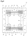
- FIGS. 8 and 10 are plan views showing the solid-state image pickup element mounting structures according to an embodiment of the present invention.
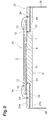
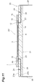
- Figs. 9 and 11 are drawings illustrating cross-sectional configurations in the solid-state image pickup element mounting structures according to the present embodiment.
- the solid-state image pickup element IS1 is mounted on the mounting member 20 (the intended mounting region 22 of the substrate 21) so that the principal face 1b (the back face to the principal face 1a) is opposite to the principal face 21 a of the mounting member 20 (substrate 21).
- the semiconductor substrate 1 of the solid-state image pickup element IS1 and the substrate 21 of the mounting member 20 are bonded to each other with a resin (e.g., epoxy resin, urethane resin, silicone resin, or acrylic resin, or a complex of these) R.
- the first electrode pads 10 and the electrode pads 24 are connected by wire bonding.
- the solid-state image pickup element IS2 is mounted on the mounting member 20 (the intended mounting region 22 of the substrate 21) so that the principal face 1a is opposite to the principal face 21 a of the mounting member 20 (substrate 21).
- the semiconductor substrate 1 of the solid-state image pickup element IS2 and the substrate 21 of the mounting member 20 are bonded to each other with the resin R.
- the second electrode pads 12 and the electrode pads 23 are connected by flip chip bonding.
- Fig. 12 is a plan view showing the mounting member according to an embodiment of the present invention.
- Fig. 13 is a drawing illustrating a cross-sectional configuration of the mounting member according to the present embodiment.
- the mounting member 30 is a so-called interposer and is provided with a substrate 31 of a rectangular shape on the plan view.
- the substrate 31 includes principal faces 31a, 31b opposed to each other.
- In the substrate 31 there are a plurality of electrode pads 33, 34 arranged at predetermined positions on the principal face 31 a and a plurality of electrode pads 35 arranged at predetermined positions on the principal face 31b.
- Internal interconnections 36 are arranged inside the substrate 31.
- the mounting member 30 is arranged in a housing space of a package 40 and is mounted through a pedestal 41 on a bottom portion of the package 40.
- a plurality of electrode pads 43 are arranged at predetermined positions thereof.
- Internal interconnections 45 are arranged in the frame portion of the package 40 and external terminals 46 are arranged on side faces of the package 40.
- the corresponding electrode pad 43 and external terminal 46 are electrically connected to each other by an internal interconnection 45.
- the electrode pads 43 are formed by a method such as printing or sputtering, using an electroconductive material such as metal.
- the package 40 is provided with a window part (not shown) arranged opposite to the mounting member 30.
- a Peltier element may be used instead of the pedestal 41.
- Each electrode pad 33 is arranged outside an intended mounting region 32 on the principal face 31a of the substrate 31.
- the intended mounting region 32 herein is a region on which the solid-state image pickup element IS1 or IS2 is to be mounted, and has a rectangular shape located approximately in the center of the substrate 31 of the rectangular shape on the plan view.
- the electrode pads 33 each are arrayed in a line outside the intended mounting region 32.
- the electrode pads 33 are to be connected to the first electrode pads 10 of the front-illuminated solid-state image pickup element IS1.
- the positions of the electrode pads 33 correspond to the array positions of the first electrode pads 10 of the solid-state image pickup element IS1 to be mounted.
- Each electrode pad 34 is arranged at the edge portion of the mounting member 30 on the principal face 31a of the substrate 31.
- the electrode pads 34 are arrayed in a line along the edge potion of the mounting member 30.
- the electrode pads 34 are connected to the electrode pads 43 of the package 40 by wire bonding.
- the positions of the electrode pads 34 correspond to the array positions of the electrode pads 43 of the package 40.
- the electrode pads 34 are provided as many as the electrode pads 43.
- Each electrode pad 35 is arranged inside a region corresponding to the intended mounting region 32 on the principal face 31b of the substrate 31.
- the electrode pads 35 each are arrayed in a line inside the region corresponding to the intended mounting region 32.
- the electrode pads 35 are provided as many as the electrode pads 33 and as many as the electrode pads 34 as well.
- the electrode pads 35 are to be connected to the second electrode pads 12 of the back-illuminated solid-state image pickup element IS2.
- the positions of the electrode pads 35 correspond to the array positions of the second electrode pads 12 of the solid-state image pickup element IS2 to be mounted.
- the electrode pads 33, 34, and 35 are formed by a method such as printing or sputtering, using an electroconductive material such as metal.
- the mounting member 30 there are through holes 37 formed for connecting the second electrode pads 12 of the solid-state image pickup element IS2 to the electrode pads 35 by wire bonding.
- the through holes 37 are formed along the array of electrode pads 35.
- the through holes 37 are formed at positions where the second electrode pads 12 of the solid-state image pickup element IS2 to be mounted on the mounting member 30 face the through holes 37.
- the corresponding electrode pad 33, electrode pad 34, and electrode pad 35 are electrically connected to each other by an internal interconnection 36.
- a common input/output signal is transmitted through the internal interconnection 36, electrode pad 35, bonding wire, electrode pad 43, internal interconnection 45, and external terminal 26 to the corresponding electrode pad 33 and electrode pad 35.
- FIGS. 14 and 16 are plan views showing the solid-state image pickup element mounting structures according to an embodiment of the present invention.
- Figs. 15 and 17 are drawings illustrating cross-sectional configurations in the solid-state image pickup element mount structures according to the present embodiment.
- the solid-state image pickup element IS1 is mounted on the mounting member 30 (the intended mounting region 32 of the substrate 31) so that the principal face 1b (the back face to the principal face 1a) is opposite to the principal face 31a of the mounting member 30 (substrate 31).
- the semiconductor substrate 1 of the solid-state image pickup element IS1 and the substrate 31 of the mounting member 30 are bonded to each other with a resin.
- the first electrode pads 10 and the electrode pads 33 are connected by wire bonding.
- the solid-state image pickup element IS2 is mounted on the mounting member 30 (the intended mounting region 32 of the substrate 31) so that the principal face 1 a is opposite to the principal face 31a of the mounting member 30 (substrate 31).
- the semiconductor substrate 1 of the solid-state image pickup element IS2 and the substrate 31 of the mounting member 30 are bonded to each other with the resin.
- the second electrode pads 12 and the electrode pads 35 are connected through the through holes 37 by wire bonding.
- the first electrode pad 10 and the second electrode pad 12 in the positional relation of line symmetry with respect to the center line l perpendicular to the array directions of the plurality of first and second electrode pads 10, 12 are connected through the interconnection 14.
- the first electrode pad 10 and the second electrode pad 12 in the same order relation in the array order in the first direction along the sides 2a, 2b among the plurality of first electrode pads 10 and in the array order in the second direction along the sides 2a, 2b among the plurality of second electrode pads 12 are connected through the interconnection 14. Therefore, even with reversal of the principal face 1a and the principal face 1b, the positions of the first electrode pads 10 and the second electrode pads 12 connected to each other through the interconnections 14 are the same in the array directions of the respective electrode pads 10, 12.
- the plurality of first electrode pads 10 are located nearer to the edge of the semiconductor substrate 1 than the plurality of second electrode pads 12 are. Namely, the plurality of first electrode pads 10 are located nearer to the sides 2a, 2b of the semiconductor substrate 1 than the plurality of second electrode pads 12 are. This facilitates the connection by wire bonding to each first electrode pad 10, in mounting the solid-state image pickup element IS1 with the principal face 1b being opposite to the mounting member 20, 30.
- the first and second electrode pads 10, 12 are arranged in the respective regions near to the two opposed sides 2a, 2b with the photosensitive region 3 in between them, but there is no need for being limited to this.
- the first and second electrode pads 10, 12 may be formed in a region near to one side 2a or 2b out of the two sides 2a and 2b.
- first and second electrode pads 10, 12 are not limited to those disclosed in the above embodiments, either.
- the first and second electrode pads 10, 12 do not have to be arranged in the zigzag patterns but may be arranged in a line or in parallel lines.
- the present invention is applicable to the front-illuminated or back-illuminated solid-state image pickup elements and the mounting structures thereof.
- 1 semiconductor substrate 1a, 1b principal faces; 2a-2d sides; 3 photosensitive region; 10 first electrode pads; 12 second electrode pads;
Landscapes
- Solid State Image Pick-Up Elements (AREA)
- Transforming Light Signals Into Electric Signals (AREA)
Abstract
Description
- The present invention relates to a solid-state image pickup element and a solid-state image pickup element mounting structure.
- A known solid-state image pickup element is a so-called front-illuminated solid-state image pickup element provided with a semiconductor substrate having a sensitive region, and a plurality of electrode pads arrayed on a principal face of the semiconductor substrate, wherein the principal face side of the semiconductor substrate is a light receiving surface side (e.g., cf. Patent Literature 1). Another known solid-state image pickup element is a so-called back-illuminated solid-state image pickup element provided with a semiconductor substrate having a sensitive region, and a plurality of electrode pads arrayed on a principal face of the semiconductor substrate, wherein the back face side to the principal face of the semiconductor substrate is a light receiving surface side (e.g., cf. Patent Literature 2).
- Patent Literature 1: Japanese Patent Application Laid-Open Publication No.
H10-107255 - Patent Literature 2: Japanese Patent Application Laid-Open Publication No.
H06-045574 - In comparison between the foregoing front-illuminated solid-state image pickup element and back-illuminated solid-state image pickup element, a surface of the former to be opposed to a mounting member (e.g., a wiring substrate or the like) on which the solid-state image pickup element is to be mounted is reverse to that of the latter and an arrangement of the electrode pads arrayed on the principal face of the semiconductor substrate in the former is also reverse to that in the latter. If the front-illuminated solid-state image pickup element and back-illuminated solid-state image pickup element are intended to be mounted on the mounting member of the same structure, an arrangement of output terminals of the mounting member to be electrically connected to the electrode pads in the former solid-state image pickup element will be also reverse to that in the latter. For this reason, it is necessary to prepare two types of external circuits (e.g., drive circuits or the like) to be connected to the solid-state image pickup element through the mounting member, according to the arrangements of output terminals of the mounting member.
- For adopting a common external circuit to the front-illuminated solid-state image pickup element and the back-illuminated solid-state image pickup element, the same arrangement of output terminals must be used for the front-illuminated solid-state image pickup element and the back-illuminated solid-state image pickup element. This requires us to prepare the mounting member for the front-illuminated solid-state image pickup element and the mounting member for the back-illuminated solid-state image pickup element. In either case, we need to prepare two types of external circuits or mounting members or the like, which leads to increase in cost and preparatory period of the external circuits or the mounting members or the like.
- It is an object of the present invention to provide a solid-state image pickup element and a solid-state image pickup element mounting structure allowing easy reduction of the cost and preparatory period of the external circuit or the mounting member or the like.
- An aspect of the present invention is a solid-state image pickup element comprising: a semiconductor substrate having a photosensitive region; a plurality of first electrode pads arrayed on a principal face of the semiconductor substrate; a plurality of second electrode pads arrayed in a direction along a direction in which the plurality of first electrode pads are arrayed, on the principal face of the semiconductor substrate; and a plurality of interconnections connecting the plurality of first electrode pads and the plurality of second electrode pads in one-to-one correspondence, wherein the plurality of interconnections connect the first and second electrode pads so that each interconnection connects the first electrode pad and the second electrode pad in a positional relation of line symmetry with respect to a center line perpendicular to the array directions of the plurality of first and second electrode pads.
- In the present invention, the first electrode pad and the second electrode pad in the positional relation of line symmetry with respect to the center line perpendicular to the array directions of the plurality of first and second electrode pads are connected through the interconnection. Therefore, even with reversal of the principal face and the back face to this principal face, the positions of the first electrode pad and the second electrode pad connected to each other through the interconnection are the same in the array directions of the respective electrode pads.
- In comparison between a case where this solid-state image pickup element is mounted on a mounting member with the principal face being opposite thereto and a case where the solid-state image pickup element is mounted on the mounting member with the back face to the principal face being opposite thereto, there is no reversal of the positional relation of terminals of the mounting member to be electrically connected to the first electrode pads or to the second electrode pads. As a result, there is no need for preparing two types of external circuits such as the drive circuits and no need for preparing two types of mounting members, either. Therefore, the present invention allows easy reduction of the cost and preparatory period of the external circuit or the mounting member or the like.
- The plurality of first electrode pads may be located nearer to an edge of the semiconductor substrate than the plurality of second electrode pads are. In this case, the connection by wire bonding to each first electrode pad becomes easier when the solid-state image pickup element is mounted on the mounting member with the back face to the principal face being opposite thereto.
- Another aspect of the present invention is a solid-state image pickup element comprising: a semiconductor substrate of a rectangular shape having a photosensitive region; a plurality of first electrode pads arrayed in a first direction along one side of the semiconductor substrate, on a principal face of the semiconductor substrate; a plurality of second electrode pads arrayed in the first direction on the principal face of the semiconductor substrate; and a plurality of interconnections connecting the plurality of first electrode pads and the plurality of second electrode pads in one-to-one correspondence, wherein the plurality of interconnections connect the first and second electrode pads so that each interconnection connects the first electrode pad and the second electrode pad in an identical order relation in an array order in the first direction among the plurality of first electrode pads and in an array order in a second direction opposite to the first direction among the plurality of second electrode pads.
- In the present invention, the first electrode pad and the second electrode pad in the same order relation in the array order in the first direction among the plurality of first electrode pads and in the array order in the second direction among the plurality of second electrode pads are connected through the interconnection. Therefore, even with reversal of the principal face of the semiconductor substrate and the back face to this principal face, the positions of the first electrode pad and the second electrode pad connected to each other through the interconnection are the same in the array orders of the respective electrode pads.
- In comparison between a case where this solid-state image pickup element is mounted on a mounting member with the principal face being opposite thereto and a case where the solid-state image pickup element is mounted on the mounting member with the back face to the principal face being opposite thereto, there is no reversal of the positional relation of terminals of the mounting member to be electrically connected to the first electrode pads or to the second electrode pads. As a result, there is no need for preparing two types of external circuits such as the drive circuits and no need for preparing two types of mounting members, either. Therefore, the present invention allows easy reduction of the cost and preparatory period of the external circuit or the mounting member or the like.
- The plurality of first electrode pads may be located nearer to the aforementioned one side of the semiconductor substrate than the plurality of second electrode pads are. In this case, the connection by wire bonding to each first electrode pad becomes easier when the solid-state image pickup element is mounted on the mounting member with the back face to the principal face being opposite thereto.
- The semiconductor substrate may have a light receiving surface side defined on the principal face side and the semiconductor substrate may have a light receiving surface side defined on the the back face side to the principal face. When the principal face side is the light receiving surface side, the front-illuminated solid-state image pickup element is realized. When the back face side to the principal face is the light receiving surface side, the back-illuminated solid-state image pickup element is realized.
- Still another aspect of the present invention is a solid-state image pickup element mounting structure comprising: the aforementioned solid-state image pickup element; and a mounting member on which the solid-state image pickup element is mounted and in which a plurality of third electrode pads are arranged on a principal face thereof, wherein the solid-state image pickup element is mounted on the mounting member so that the back face to the principal face of the solid-state image pickup element is opposite to the principal face of the mounting member, and wherein the plurality of first electrode pads and the plurality of third electrode pads are connected by wire bonding.
- Another aspect of the present invention is a solid-state image pickup element mounting structure comprising: the foregoing solid-state image pickup element; and a mounting member on which the solid-state image pickup element is mounted and in which a plurality of third electrode pads are arranged on a principal face thereof, wherein the solid-state image pickup element is mounted on the mounting member so that the principal face of the solid-state image pickup element is opposite to the principal face of the mounting member, and wherein the plurality of second electrode pads and the plurality of third electrode pads are connected by flip chip bonding.
- Another aspect of the present invention is a solid-state image pickup element mounting structure comprising: the foregoing solid-state image pickup element; and a mounting member on which the solid-state image pickup element is mounted and in which a plurality of third electrode pads are arranged on a principal face thereof, wherein the solid-state image pickup element is mounted on the mounting member so that the principal face of the solid-state image pickup element is opposite to a back face to the principal face of the mounting member, and wherein the plurality of second electrode pads and the plurality of third electrode pads are connected by wire bonding.
- With any one of the solid-state image pickup element mounting structures, there is no need for preparing two types of external circuits or mounting members or the like, as described above. Therefore, the present invention allows easy reduction of the cost and preparatory period of the external circuit or the mounting member or the like.
- The present invention provides the solid-state image pickup elements and the solid-state image pickup element mounting structures allowing easy reduction of the cost and preparatory period of the external circuit or the mounting member or the like.
-
-
Fig. 1 is a plan view showing a front-illuminated solid-state image pickup element according to an embodiment of the present invention. -
Fig. 2 is a drawing illustrating a cross-sectional configuration of the front-illuminated solid-state image pickup element according to the embodiment. -
Fig. 3 is a plan view showing a back-illuminated solid-state image pickup element according to an embodiment of the present invention. -
Fig. 4 is a drawing illustrating a cross-sectional configuration of the back-illuminated solid-state image pickup element according to the embodiment. -
Fig. 5 is a perspective plan view for illustrating first and second electrode pads in the back-illuminated solid-state image pickup element according to the embodiment. -
Fig. 6 is a plan view showing a mounting member according to an embodiment of the present invention. -
Fig. 7 is a drawing illustrating a cross-sectional configuration of the mounting member according to the embodiment. -
Fig. 8 is a plan view showing a solid-state image pickup element mounting structure according to an embodiment of the present invention. -
Fig. 9 is a drawing illustrating a cross-sectional configuration in the solid-state image pickup element mounting structure according to the embodiment. -
Fig. 10 is a plan view showing a solid-state image pickup element mounting structure according to an embodiment of the present invention. -
Fig. 11 is a drawing illustrating a cross-sectional configuration in the solid-state image pickup element mounting structure according to the embodiment. -
Fig. 12 is a plan view showing a mounting member according to an embodiment of the present invention. -
Fig. 13 is a drawing illustrating a cross-sectional configuration of the mounting member according to the embodiment. -
Fig. 14 is a plan view showing a solid-state image pickup element mounting structure according to an embodiment of the present invention. -
Fig. 15 is a drawing illustrating a cross-sectional configuration in the solid-state image pickup element mounting structure according to the embodiment. -
Fig. 16 is a plan view showing a solid-state image pickup element mounting structure according to the embodiment. -
Fig. 17 is a drawing illustrating a cross-sectional configuration in the solid-state image pickup element mounting structure according to the embodiment. - The preferred embodiments of the present invention will be described below in detail with reference to the accompanying drawings. In the description, the same elements or elements with the same functionality will be denoted by the same reference signs, without redundant description.
- First, a configuration of a front-illuminated solid-state image pickup element IS1 according to an embodiment of the present invention will be described with reference to
Figs. 1 and2 .Fig. 1 is a plan view showing the front-illuminated solid-state image pickup element according to the present embodiment.Fig. 2 is a drawing illustrating a cross-sectional configuration of the front-illuminated solid-state image pickup element according to the present embodiment. - The front-illuminated solid-state image pickup element IS 1, as shown in
Figs. 1 and2 , is provided with asemiconductor substrate 1, a plurality offirst electrode pads 10, a plurality ofsecond electrode pads 12, and a plurality ofinterconnections 14. The solid-state image pickup element IS1 is a so-called FI (Front-Illuminated)-CCD image sensor. The illustration of theinterconnections 14 is omitted fromFig. 2 . - The
semiconductor substrate 1 has a rectangular shape on the plane view and has foursides 2a-2d constituting the edge of thesemiconductor substrate 1. Thesemiconductor substrate 1 includes principal faces 1a, 1b opposed to each other. Thesemiconductor substrate 1 has a photosensitive region (image pickup region) 3 formed on theprincipal face 1a side. In thephotosensitive region 3, a CCD for image pickup consisting of a plurality of vertical shift registers (not shown) is formed as pixels. In the solid-state image pickup element IS1, theprincipal face 1a side is a light receiving surface side.Fig. 1 is the plan view of the solid-state image pickup element IS1 as viewed from the light receiving surface (principal face 1a) side. - A light image incident on the
photosensitive region 3 is converted into a two-dimensional electric charge image and electric charges are transferred along the vertical direction by the vertical shift registers. A horizontal shift register (not shown) is provided at an end in the charge transfer direction of thephotosensitive region 3. The electric charges of the respective pixels having been transferred in the vertical direction are sequentially transferred along the horizontal direction by the horizontal shift register. The charge transfer method of the CCD may be a known method such as the frame transfer method, the interline transfer method, or the full frame transfer method. - Each
first electrode pad 10 is arranged on theprincipal face 1a of thesemiconductor substrate 1. Eachfirst electrode pad 10 is provided in one of regions near to the twoopposed sides photosensitive region 3 in between thefirst electrode pads 10. In the present embodiment, twelvefirst electrode pads 10 are provided in each of the regions near to therespective sides first electrode pads 10 provided. Thefirst electrode pads 10 each are arrayed in a direction along thesides semiconductor substrate 1. Thefirst electrode pads 10 have a rectangular shape. - Each
second electrode pad 12 is also arranged on theprincipal face 1a of thesemiconductor substrate 1. Eachsecond electrode pad 12 is provided in one of the regions near to the foregoing twosides sides semiconductor substrate 1 as thefirst electrode pads 10 are. In the present embodiment, twelvesecond electrode pads 12 are provided in each of the regions near to therespective sides second electrode pads 12 provided. Thesecond electrode pads 12 have a circular shape. Thefirst electrode pads 10 are located nearer to the edge of thesemiconductor substrate 1 or nearer to thesides second electrode pads 12 are. - The
first electrode pads 10 and thesecond electrode pads 12 are arranged in zigzag patterns. Thefirst electrode pads 10 and thesecond electrode pads 12 each include electrode pads for applying a transfer voltage to charge transfer electrodes for transferring electric charges in the vertical direction, an electrode pad for applying a transfer voltage to a charge transfer electrode for transferring electric charges in the horizontal direction, an electrode pad for reading out the electric charges having been transferred in the horizontal direction, an electrode pad for extracting outputs, an electrode pad for execution of a test operation, and so on. - Each
interconnection 14, as shown inFig. 1 , is provided on thesemiconductor substrate 1 and connects thefirst electrode pad 10 and thesecond electrode pad 12 in one-to-one correspondence. Eachinterconnection 14 connects thefirst electrode pad 10 and thesecond electrode pad 12 in a positional relation of line symmetry with respect to a center line l perpendicular to the array directions of the first andsecond electrode pads interconnection 14 connects thefirst electrode pad 10 and thesecond electrode pad 12 in an identical order relation in an array order in a first direction (e.g., a direction from theside 2c to theside 2d) along theside 2a (or theside 2b) among thefirst electrode pads 10 and in an array order in a second direction (e.g., a direction from theside 2d to theside 2c) opposite to the first direction.Fig. 1 is drawn without the illustration of interconnections electrically connecting thephotosensitive region 3 and each of theelectrode pads - Next, a configuration of a back-illuminated solid-state image pickup element IS2 according to an embodiment of the present invention will be described with reference to
Figs. 3 and4 .Fig. 3 is a plan view showing the back-illuminated solid-state image pickup element according to the present embodiment.Fig. 4 is a drawing illustrating a cross-sectional view of the back-illuminated solid-state image pickup element according to the present embodiment. The illustration of theinterconnections 14 is omitted fromFig. 4 . - The back-illuminated solid-state image pickup element IS2, as shown in
Figs. 3 and4 , is provided with thesemiconductor substrate 1, the plurality offirst electrode pads 10, the plurality ofsecond electrode pads 12, and the plurality ofinterconnections 14 as the solid-state image pickup element IS1 is. The solid-state image pickup element IS2 is a so-called BT (Back-Thinned)-CCD image sensor. - The
semiconductor substrate 1 is thinned by etching a central region thereof with an aqueous KOH solution from theprincipal face 1b side. This thinning results in forming a recess portion on theprincipal face 1b side in the central region of thesemiconductor substrate 1. A frame portion thicker than the recess portion is present around the recess portion of thesemiconductor substrate 1. The frame portion may be removed by etching whereby the solid-state image pickup element IS2 is constructed as a BT-CCD image sensor wherein the entire region of thesemiconductor substrate 1 is thinned. - In the solid-state image pickup element IS2, the
principal face 1b side is the light receiving surface side.Fig. 3 is the plan view of the solid-state image pickup element IS2 as viewed from the back face (principal face 1a) side to the light receiving surface.Fig. 3 , likeFig. 1 , is drawn without the illustration of interconnections electrically connecting thephotosensitive region 3 and each of theelectrode pads - In the solid-state image pickup element IS2 as well, as shown in
Fig. 3 , eachinterconnection 14 connects thefirst electrode pad 10 and thesecond electrode pad 12 in a positional relation of line symmetry with respect to the center line l perpendicular to the array directions of the first andsecond electrode pads principal face 1b) side, as shown inFig. 5 , the positions (array order) in the array direction of the respectivefirst electrode pads 10 in the solid-state image pickup element IS2 are the same as the positions (array order) in the array direction of thesecond electrode pads 12 connected through theinterconnections 14 to the correspondingfirst electrode pads 10 in the solid-state image pickup element IS 1. Similarly, when the solid-state image pickup element IS2 is seen through from the light receiving surface (principal face 1b) side, the positions (array order) in the array direction of the respectivesecond electrode pads 12 in the solid-state image pickup element IS2 are the same as the positions (array order) in the array direction of thefirst electrode pads 10 connected through theinterconnections 14 to the correspondingsecond electrode pads 12 in the solid-state image pickup element IS 1. - Next, a configuration of a mounting
member 20 on which the solid-state image pickup element IS1 or IS2 is to be mounted will be described with reference toFigs. 6 and7 .Fig. 6 is a plan view showing the mounting member according to the present embodiment.Fig. 7 is a drawing illustrating a cross-sectional configuration of the mounting member according to the present embodiment. - The mounting
member 20 is a so-called package and is provided with asubstrate 21 of a rectangular shape on the plan view. Thesubstrate 21 includes principal faces 21a, 21b opposed to each other. In thesubstrate 21, there are a plurality ofelectrode pads principal face 21a thereof.Internal interconnections 25 are arranged inside thesubstrate 21 andexternal terminal 26 are arranged on side faces of thesubstrate 21. - Each
electrode pad 23 is arranged inside an intended mountingregion 22 on theprincipal face 21 a of thesubstrate 21. The intended mountingregion 22 herein is a region on which the solid-state image pickup element IS 1 or IS2 is intended to be mounted, and has a rectangular shape located approximately in the center of thesubstrate 21 of the rectangular shape on the plan view. Theelectrode pads 23 are arrayed in a line as aligned along the peripheral edge portion of the intended mountingregion 22. Theelectrode pads 23 are to be connected to thesecond electrode pads 12 of the back-illuminated solid-state image pickup element IS2. The positions of theelectrode pads 23 correspond to the array positions of thesecond electrode pads 12 of the solid-state image pickup element IS2 to be mounted. Theelectrode pads 23 have a circular shape. - Each
electrode pad 24 is arranged outside the intended mountingregion 22 on theprincipal face 21a of thesubstrate 21. Namely, theelectrode pads 24 each are arrayed in a line outside the intended mountingregion 22. Theelectrode pads 24 are provided as many as theelectrode pads 23. Theelectrode pads 24 are to be connected to thefirst electrode pads 10 of the front-illuminated solid-state image pickup element IS 1. The positions of theelectrode pads 24 correspond to the array positions of thefirst electrode pads 10 of the solid-state image pickup element IS1 to be mounted. Theelectrode pads electrode pads 24 have a rectangular shape. - The corresponding
electrode pad 23 andelectrode pad 24 are electrically connected to each other by aninternal interconnection 25. Theinternal interconnections 25 are electrically connected respectively to the plurality ofexternal terminals 26 arranged so as to extend downward from the side faces of thesubstrate 21. As a consequence, a common input/output signal is transmitted through theinternal interconnection 25 and theexternal terminal 26 to thecorresponding electrode pads - Next, mounting structures of the solid-state image pickup elements IS1 and IS2 using the mounting
member 20 will be described with reference toFigs. 8 to 11 .Figs. 8 and10 are plan views showing the solid-state image pickup element mounting structures according to an embodiment of the present invention.Figs. 9 and11 are drawings illustrating cross-sectional configurations in the solid-state image pickup element mounting structures according to the present embodiment. - As shown in
Figs. 8 and9 , the solid-state image pickup element IS1 is mounted on the mounting member 20 (the intended mountingregion 22 of the substrate 21) so that theprincipal face 1b (the back face to theprincipal face 1a) is opposite to theprincipal face 21 a of the mounting member 20 (substrate 21). Thesemiconductor substrate 1 of the solid-state image pickup element IS1 and thesubstrate 21 of the mountingmember 20 are bonded to each other with a resin (e.g., epoxy resin, urethane resin, silicone resin, or acrylic resin, or a complex of these) R. Thefirst electrode pads 10 and theelectrode pads 24 are connected by wire bonding. - As shown in
Figs. 10 and11 , the solid-state image pickup element IS2 is mounted on the mounting member 20 (the intended mountingregion 22 of the substrate 21) so that theprincipal face 1a is opposite to theprincipal face 21 a of the mounting member 20 (substrate 21). Thesemiconductor substrate 1 of the solid-state image pickup element IS2 and thesubstrate 21 of the mountingmember 20 are bonded to each other with the resin R. Thesecond electrode pads 12 and theelectrode pads 23 are connected by flip chip bonding. - Next, a configuration of a mounting
member 30 on which the solid-state image pickup element IS1 or IS2 is to be mounted, will be described with reference toFigs. 12 and13 .Fig. 12 is a plan view showing the mounting member according to an embodiment of the present invention.Fig. 13 is a drawing illustrating a cross-sectional configuration of the mounting member according to the present embodiment. - The mounting
member 30 is a so-called interposer and is provided with asubstrate 31 of a rectangular shape on the plan view. Thesubstrate 31 includes principal faces 31a, 31b opposed to each other. In thesubstrate 31 there are a plurality ofelectrode pads principal face 31 a and a plurality ofelectrode pads 35 arranged at predetermined positions on theprincipal face 31b.Internal interconnections 36 are arranged inside thesubstrate 31. - The mounting
member 30 is arranged in a housing space of apackage 40 and is mounted through apedestal 41 on a bottom portion of thepackage 40. On a frame portion of thepackage 40, a plurality ofelectrode pads 43 are arranged at predetermined positions thereof.Internal interconnections 45 are arranged in the frame portion of thepackage 40 andexternal terminals 46 are arranged on side faces of thepackage 40. The correspondingelectrode pad 43 andexternal terminal 46 are electrically connected to each other by aninternal interconnection 45. Theelectrode pads 43 are formed by a method such as printing or sputtering, using an electroconductive material such as metal. Thepackage 40 is provided with a window part (not shown) arranged opposite to the mountingmember 30. A Peltier element may be used instead of thepedestal 41. - Each
electrode pad 33 is arranged outside an intended mountingregion 32 on theprincipal face 31a of thesubstrate 31. The intended mountingregion 32 herein is a region on which the solid-state image pickup element IS1 or IS2 is to be mounted, and has a rectangular shape located approximately in the center of thesubstrate 31 of the rectangular shape on the plan view. Theelectrode pads 33 each are arrayed in a line outside the intended mountingregion 32. Theelectrode pads 33 are to be connected to thefirst electrode pads 10 of the front-illuminated solid-state image pickup element IS1. The positions of theelectrode pads 33 correspond to the array positions of thefirst electrode pads 10 of the solid-state image pickup element IS1 to be mounted. - Each
electrode pad 34 is arranged at the edge portion of the mountingmember 30 on theprincipal face 31a of thesubstrate 31. Theelectrode pads 34 are arrayed in a line along the edge potion of the mountingmember 30. Theelectrode pads 34 are connected to theelectrode pads 43 of thepackage 40 by wire bonding. The positions of theelectrode pads 34 correspond to the array positions of theelectrode pads 43 of thepackage 40. Theelectrode pads 34 are provided as many as theelectrode pads 43. - Each
electrode pad 35 is arranged inside a region corresponding to the intended mountingregion 32 on theprincipal face 31b of thesubstrate 31. Theelectrode pads 35 each are arrayed in a line inside the region corresponding to the intended mountingregion 32. Theelectrode pads 35 are provided as many as theelectrode pads 33 and as many as theelectrode pads 34 as well. Theelectrode pads 35 are to be connected to thesecond electrode pads 12 of the back-illuminated solid-state image pickup element IS2. The positions of theelectrode pads 35 correspond to the array positions of thesecond electrode pads 12 of the solid-state image pickup element IS2 to be mounted. Theelectrode pads - In the mounting
member 30 there are throughholes 37 formed for connecting thesecond electrode pads 12 of the solid-state image pickup element IS2 to theelectrode pads 35 by wire bonding. The through holes 37 are formed along the array ofelectrode pads 35. The through holes 37 are formed at positions where thesecond electrode pads 12 of the solid-state image pickup element IS2 to be mounted on the mountingmember 30 face the through holes 37. - The corresponding
electrode pad 33,electrode pad 34, andelectrode pad 35 are electrically connected to each other by aninternal interconnection 36. As a consequence, a common input/output signal is transmitted through theinternal interconnection 36,electrode pad 35, bonding wire,electrode pad 43,internal interconnection 45, andexternal terminal 26 to thecorresponding electrode pad 33 andelectrode pad 35. - Next, mounting structures of the solid-state image pickup elements IS1 and IS2 using the mounting
member 30 will be described with reference toFigs. 14 to 17 .Figs. 14 and16 are plan views showing the solid-state image pickup element mounting structures according to an embodiment of the present invention.Figs. 15 and17 are drawings illustrating cross-sectional configurations in the solid-state image pickup element mount structures according to the present embodiment. - As shown in
Figs. 14 and15 , the solid-state image pickup element IS1 is mounted on the mounting member 30 (the intended mountingregion 32 of the substrate 31) so that theprincipal face 1b (the back face to theprincipal face 1a) is opposite to theprincipal face 31a of the mounting member 30 (substrate 31). Thesemiconductor substrate 1 of the solid-state image pickup element IS1 and thesubstrate 31 of the mountingmember 30 are bonded to each other with a resin. Thefirst electrode pads 10 and theelectrode pads 33 are connected by wire bonding. - As shown in
Figs. 16 and17 , the solid-state image pickup element IS2 is mounted on the mounting member 30 (the intended mountingregion 32 of the substrate 31) so that theprincipal face 1 a is opposite to theprincipal face 31a of the mounting member 30 (substrate 31). Thesemiconductor substrate 1 of the solid-state image pickup element IS2 and thesubstrate 31 of the mountingmember 30 are bonded to each other with the resin. Thesecond electrode pads 12 and theelectrode pads 35 are connected through the throughholes 37 by wire bonding. - In the embodiments of the present invention, as described above, the
first electrode pad 10 and thesecond electrode pad 12 in the positional relation of line symmetry with respect to the center line l perpendicular to the array directions of the plurality of first andsecond electrode pads interconnection 14. Namely, thefirst electrode pad 10 and thesecond electrode pad 12 in the same order relation in the array order in the first direction along thesides first electrode pads 10 and in the array order in the second direction along thesides second electrode pads 12 are connected through theinterconnection 14. Therefore, even with reversal of theprincipal face 1a and theprincipal face 1b, the positions of thefirst electrode pads 10 and thesecond electrode pads 12 connected to each other through theinterconnections 14 are the same in the array directions of therespective electrode pads - In comparison between the case where the
principal face 1b of the solid-state image pickup element IS1 is mounted opposite to the mountingmember principal face 1a of the solid-state image pickup element IS2 is mounted opposite to the mountingmember external terminals 26 of the mountingmember 20 electrically connected to thefirst electrode pads 10 or to thesecond electrode pads 12 and the positional relation between theelectrode pads 34 of the mountingmember 30 and theexternal terminals 46 of thepackage 40. As a consequence of this, there is no need for preparing two types of external circuits such as the drive circuits and no need for preparing two types of mountingmembers - In the embodiments of the present invention, the plurality of
first electrode pads 10 are located nearer to the edge of thesemiconductor substrate 1 than the plurality ofsecond electrode pads 12 are. Namely, the plurality offirst electrode pads 10 are located nearer to thesides semiconductor substrate 1 than the plurality ofsecond electrode pads 12 are. This facilitates the connection by wire bonding to eachfirst electrode pad 10, in mounting the solid-state image pickup element IS1 with theprincipal face 1b being opposite to the mountingmember - The above described the preferred embodiments of the present invention but it should be noted that the present invention is by no means limited to the foregoing embodiments and can be modified in many ways without departing from the spirit and scope of the invention.
- The first and
second electrode pads opposed sides photosensitive region 3 in between them, but there is no need for being limited to this. For example, the first andsecond electrode pads side sides - The numbers and the array numbers of first and
second electrode pads second electrode pads - The present invention is applicable to the front-illuminated or back-illuminated solid-state image pickup elements and the mounting structures thereof.
- 1 semiconductor substrate; 1a, 1b principal faces; 2a-2d sides; 3 photosensitive region; 10 first electrode pads; 12 second electrode pads;
- 14 interconnections; 20 mounting member; 21a, 21b principal faces; 23, 24 electrode pads; 30 mounting member; 31a, 31b principal faces; 33, 35 electrode pads; 46 external terminals; IS1, IS2 solid-state image pickup elements; 1 center line.
Claims (9)
- A solid-state image pickup element comprising:a semiconductor substrate having a photosensitive region;a plurality of first electrode pads arrayed on a principal face of the semiconductor substrate;a plurality of second electrode pads arrayed in a direction along a direction in which the plurality of first electrode pads are arrayed, on the principal face of the semiconductor substrate; anda plurality of interconnections connecting the plurality of first electrode pads and the plurality of second electrode pads in one-to-one correspondence,wherein the plurality of interconnections connect the first and second electrode pads so that each interconnection connects the first electrode pad and the second electrode pad in a positional relation of line symmetry with respect to a center line perpendicular to the array directions of the plurality of first and second electrode pads.
- The solid-state image pickup element according to Claim 1,
wherein the plurality of first electrode pads are located nearer to an edge of the semiconductor substrate than the plurality of second electrode pads are. - A solid-state image pickup element comprising:a semiconductor substrate of a rectangular shape having a photosensitive region;a plurality of first electrode pads arrayed in a first direction along one side of the semiconductor substrate, on a principal face of the semiconductor substrate;a plurality of second electrode pads arrayed in the first direction on the principal face of the semiconductor substrate; anda plurality of interconnections connecting the plurality of first electrode pads and the plurality of second electrode pads in one-to-one correspondence,wherein the plurality of interconnections connect the first and second electrode pads so that each interconnection connects the first electrode pad and the second electrode pad in an identical order relation in an array order in the first direction among the plurality of first electrode pads and in an array order in a second direction opposite to the first direction among the plurality of second electrode pads.
- The solid-state image pickup element according to Claim 3,
wherein the plurality of first electrode pads are located nearer to said one side of the semiconductor substrate than the plurality of second electrode pads are. - The solid-state image pickup element according to any one of Claims 1 to 4,
wherein the semiconductor substrate has a light receiving surface side defined on the principal face side. - The solid-state image pickup element according to any one of Claims 1 to 4,
wherein the semiconductor substrate has a light receiving surface side defined on the the back face side to the principal face. - A solid-state image pickup element mounting structure comprising:the solid-state image pickup element as set forth in Claim 5; anda mounting member on which the solid-state image pickup element is mounted and in which a plurality of third electrode pads are arranged on a principal face thereof,wherein the solid-state image pickup element is mounted on the mounting member so that the back face to the principal face of the solid-state image pickup element is opposite to the principal face of the mounting member, andwherein the plurality of first electrode pads and the plurality of third electrode pads are connected by wire bonding.
- A solid-state image pickup element mounting structure comprising:the solid-state image pickup element as set forth in Claim 6; anda mounting member on which the solid-state image pickup element is mounted and in which a plurality of third electrode pads are arranged on a principal face thereof,wherein the solid-state image pickup element is mounted on the mounting member so that the principal face of the solid-state image pickup element is opposite to the principal face of the mounting member, andwherein the plurality of second electrode pads and the plurality of third electrode pads are connected by flip chip bonding.
- A solid-state image pickup element mounting structure comprising:the solid-state image pickup element as set forth in Claim 6; anda mounting member on which the solid-state image pickup element is mounted and in which a plurality of third electrode pads are arranged on a principal face thereof,wherein the solid-state image pickup element is mounted on the mounting member so that the principal face of the solid-state image pickup element is opposite to a back face to the principal face of the mounting member, andwherein the plurality of second electrode pads and the plurality of third electrode pads are connected by wire bonding.
Applications Claiming Priority (2)
| Application Number | Priority Date | Filing Date | Title |
|---|---|---|---|
| JP2011192938A JP5844580B2 (en) | 2011-09-05 | 2011-09-05 | Solid-state image sensor and mounting structure of solid-state image sensor |
| PCT/JP2012/065640 WO2013035410A1 (en) | 2011-09-05 | 2012-06-19 | Solid-state image pickup element and solid-state image pickup element mounting structure |
Publications (3)
| Publication Number | Publication Date |
|---|---|
| EP2755235A1 true EP2755235A1 (en) | 2014-07-16 |
| EP2755235A4 EP2755235A4 (en) | 2015-05-20 |
| EP2755235B1 EP2755235B1 (en) | 2017-09-06 |
Family
ID=47831864
Family Applications (1)
| Application Number | Title | Priority Date | Filing Date |
|---|---|---|---|
| EP12830624.8A Active EP2755235B1 (en) | 2011-09-05 | 2012-06-19 | Solid-state image pickup element |
Country Status (7)
| Country | Link |
|---|---|
| US (1) | US9583526B2 (en) |
| EP (1) | EP2755235B1 (en) |
| JP (1) | JP5844580B2 (en) |
| KR (1) | KR101902042B1 (en) |
| CN (1) | CN103782388B (en) |
| TW (1) | TWI544610B (en) |
| WO (1) | WO2013035410A1 (en) |
Cited By (5)
| Publication number | Priority date | Publication date | Assignee | Title |
|---|---|---|---|---|
| CN113167638A (en) * | 2018-12-12 | 2021-07-23 | 浜松光子学株式会社 | Light detection device |
| US11901379B2 (en) | 2018-12-12 | 2024-02-13 | Hamamatsu Photonics K.K. | Photodetector |
| US12080822B2 (en) | 2018-12-12 | 2024-09-03 | Hamamatsu Photonics K.K. | Photodetector and method for manufacturing photodetector |
| US12113088B2 (en) | 2018-12-12 | 2024-10-08 | Hamamatsu Photonics K.K. | Light detection device |
| US12322744B2 (en) | 2018-12-12 | 2025-06-03 | Hamamatsu Photonics K.K. | Photodetector and method for manufacturing photodetector |
Families Citing this family (3)
| Publication number | Priority date | Publication date | Assignee | Title |
|---|---|---|---|---|
| JP6184761B2 (en) * | 2013-06-11 | 2017-08-23 | 浜松ホトニクス株式会社 | Solid-state imaging device |
| CN107850678B (en) * | 2015-07-17 | 2021-05-18 | 模拟技术公司 | Detector unit for detector array of radiation imaging modality device |
| JP7171223B2 (en) * | 2018-04-27 | 2022-11-15 | キヤノン株式会社 | IMAGING UNIT AND MANUFACTURING METHOD THEREOF |
Family Cites Families (15)
| Publication number | Priority date | Publication date | Assignee | Title |
|---|---|---|---|---|
| JPH0746719B2 (en) * | 1985-12-17 | 1995-05-17 | セイコーエプソン株式会社 | Contact image sensor |
| JPH01303747A (en) * | 1988-06-01 | 1989-12-07 | Fuji Xerox Co Ltd | Wiring structure of drive circuit board in image sensor |
| SG43790A1 (en) | 1992-03-27 | 1997-11-14 | Nat Gypsum Co | Shaft wall and horizontal metal stud therefor |
| JP2651323B2 (en) | 1992-07-22 | 1997-09-10 | 浜松ホトニクス株式会社 | Semiconductor energy detector |
| JP2888207B2 (en) | 1996-10-01 | 1999-05-10 | 日本電気株式会社 | Solid-state imaging device and driving method thereof |
| EP1152448B1 (en) * | 1999-01-21 | 2009-07-15 | Hamamatsu Photonics K.K. | Electron tube |
| JP2004134578A (en) * | 2002-10-10 | 2004-04-30 | Hamamatsu Photonics Kk | Photodetector and method of manufacturing the same |
| JP2004177217A (en) * | 2002-11-26 | 2004-06-24 | Hamamatsu Photonics Kk | Radiation imaging apparatus |
| JP4231328B2 (en) * | 2003-04-24 | 2009-02-25 | 浜松ホトニクス株式会社 | Solid-state imaging device |
| JP2006041343A (en) * | 2004-07-29 | 2006-02-09 | Matsushita Electric Ind Co Ltd | Semiconductor element |
| JP4725095B2 (en) | 2004-12-15 | 2011-07-13 | ソニー株式会社 | Back-illuminated solid-state imaging device and manufacturing method thereof |
| RU2408110C2 (en) * | 2006-03-30 | 2010-12-27 | Конинклейке Филипс Электроникс, Н.В. | Radiation detector array |
| JP4451864B2 (en) * | 2006-07-11 | 2010-04-14 | 浜松ホトニクス株式会社 | Wiring board and solid-state imaging device |
| JP2009238819A (en) | 2008-03-26 | 2009-10-15 | Sony Corp | Method of forming mask for lithography, method of forming mask data for lithography, method of manufacturing back-illuminated solid-state imaging device, back-illuminated solid-state imaging device and electronic device |
| JP2009295821A (en) * | 2008-06-05 | 2009-12-17 | Panasonic Corp | Composite board having inter-substrate connection structure, solid-state image pickup device using the composite board, and method of manufacturing the solid-state image pickup device |
-
2011
- 2011-09-05 JP JP2011192938A patent/JP5844580B2/en active Active
-
2012
- 2012-06-19 KR KR1020137032040A patent/KR101902042B1/en active Active
- 2012-06-19 CN CN201280043113.9A patent/CN103782388B/en active Active
- 2012-06-19 WO PCT/JP2012/065640 patent/WO2013035410A1/en not_active Ceased
- 2012-06-19 US US14/116,852 patent/US9583526B2/en active Active
- 2012-06-19 EP EP12830624.8A patent/EP2755235B1/en active Active
- 2012-07-31 TW TW101127625A patent/TWI544610B/en active
Cited By (7)
| Publication number | Priority date | Publication date | Assignee | Title |
|---|---|---|---|---|
| CN113167638A (en) * | 2018-12-12 | 2021-07-23 | 浜松光子学株式会社 | Light detection device |
| US11901379B2 (en) | 2018-12-12 | 2024-02-13 | Hamamatsu Photonics K.K. | Photodetector |
| US11927478B2 (en) | 2018-12-12 | 2024-03-12 | Hamamatsu Photonics K.K. | Light detection device |
| CN113167638B (en) * | 2018-12-12 | 2024-06-11 | 浜松光子学株式会社 | Light detection device |
| US12080822B2 (en) | 2018-12-12 | 2024-09-03 | Hamamatsu Photonics K.K. | Photodetector and method for manufacturing photodetector |
| US12113088B2 (en) | 2018-12-12 | 2024-10-08 | Hamamatsu Photonics K.K. | Light detection device |
| US12322744B2 (en) | 2018-12-12 | 2025-06-03 | Hamamatsu Photonics K.K. | Photodetector and method for manufacturing photodetector |
Also Published As
| Publication number | Publication date |
|---|---|
| JP2013055242A (en) | 2013-03-21 |
| KR20140068803A (en) | 2014-06-09 |
| EP2755235A4 (en) | 2015-05-20 |
| CN103782388A (en) | 2014-05-07 |
| EP2755235B1 (en) | 2017-09-06 |
| TW201312735A (en) | 2013-03-16 |
| CN103782388B (en) | 2016-08-31 |
| TWI544610B (en) | 2016-08-01 |
| WO2013035410A1 (en) | 2013-03-14 |
| JP5844580B2 (en) | 2016-01-20 |
| US20140091421A1 (en) | 2014-04-03 |
| US9583526B2 (en) | 2017-02-28 |
| KR101902042B1 (en) | 2018-09-27 |
Similar Documents
| Publication | Publication Date | Title |
|---|---|---|
| US9583526B2 (en) | Solid-state image pickup element and solid-state image pickup element mounting structure | |
| CN103681703B (en) | The stacking back side illumination image sensor of 3D and manufacture method thereof | |
| US9455358B2 (en) | Image pickup module and image pickup unit | |
| US9865641B2 (en) | Solid-state imaging device, manufacturing method therefor, and imaging apparatus | |
| CN109103209B (en) | Image sensor and preparation method thereof, and electronic device | |
| EP2712173A1 (en) | Camera module | |
| US12225304B2 (en) | Expanded image sensor pixel array | |
| US10199418B2 (en) | Semiconductor photodetection device | |
| CN111684785B (en) | Camera unit and camera device | |
| US12477854B2 (en) | Image sensor signal path routing | |
| CN101490844B (en) | Wiring board and solid-state imaging device | |
| CN113994468B (en) | Imaging element unit and imaging device | |
| CN101271906B (en) | Photoreceptor integrated circuit and optoelectronic component comprising the same | |
| WO2015107849A1 (en) | Semiconductor device and imaging module |
Legal Events
| Date | Code | Title | Description |
|---|---|---|---|
| PUAI | Public reference made under article 153(3) epc to a published international application that has entered the european phase |
Free format text: ORIGINAL CODE: 0009012 |
|
| 17P | Request for examination filed |
Effective date: 20131203 |
|
| AK | Designated contracting states |
Kind code of ref document: A1 Designated state(s): AL AT BE BG CH CY CZ DE DK EE ES FI FR GB GR HR HU IE IS IT LI LT LU LV MC MK MT NL NO PL PT RO RS SE SI SK SM TR |
|
| DAX | Request for extension of the european patent (deleted) | ||
| REG | Reference to a national code |
Ref country code: DE Ref legal event code: R079 Ref document number: 602012037101 Country of ref document: DE Free format text: PREVIOUS MAIN CLASS: H01L0027140000 Ipc: H01L0027146000 |
|
| RA4 | Supplementary search report drawn up and despatched (corrected) |
Effective date: 20150422 |
|
| RIC1 | Information provided on ipc code assigned before grant |
Ipc: H01L 27/146 20060101AFI20150416BHEP Ipc: H01L 23/00 20060101ALI20150416BHEP Ipc: H04N 5/369 20110101ALI20150416BHEP |
|
| 17Q | First examination report despatched |
Effective date: 20161011 |
|
| STAA | Information on the status of an ep patent application or granted ep patent |
Free format text: STATUS: EXAMINATION IS IN PROGRESS |
|
| GRAP | Despatch of communication of intention to grant a patent |
Free format text: ORIGINAL CODE: EPIDOSNIGR1 |
|
| STAA | Information on the status of an ep patent application or granted ep patent |
Free format text: STATUS: GRANT OF PATENT IS INTENDED |
|
| INTG | Intention to grant announced |
Effective date: 20170522 |
|
| GRAS | Grant fee paid |
Free format text: ORIGINAL CODE: EPIDOSNIGR3 |
|
| GRAA | (expected) grant |
Free format text: ORIGINAL CODE: 0009210 |
|
| STAA | Information on the status of an ep patent application or granted ep patent |
Free format text: STATUS: THE PATENT HAS BEEN GRANTED |
|
| AK | Designated contracting states |
Kind code of ref document: B1 Designated state(s): AL AT BE BG CH CY CZ DE DK EE ES FI FR GB GR HR HU IE IS IT LI LT LU LV MC MK MT NL NO PL PT RO RS SE SI SK SM TR |
|
| REG | Reference to a national code |
Ref country code: GB Ref legal event code: FG4D |
|
| REG | Reference to a national code |
Ref country code: CH Ref legal event code: EP Ref country code: AT Ref legal event code: REF Ref document number: 926735 Country of ref document: AT Kind code of ref document: T Effective date: 20170915 |
|
| REG | Reference to a national code |
Ref country code: IE Ref legal event code: FG4D |
|
| REG | Reference to a national code |
Ref country code: DE Ref legal event code: R096 Ref document number: 602012037101 Country of ref document: DE |
|
| REG | Reference to a national code |
Ref country code: NL Ref legal event code: MP Effective date: 20170906 |
|
| REG | Reference to a national code |
Ref country code: LT Ref legal event code: MG4D |
|
| PG25 | Lapsed in a contracting state [announced via postgrant information from national office to epo] |
Ref country code: NO Free format text: LAPSE BECAUSE OF FAILURE TO SUBMIT A TRANSLATION OF THE DESCRIPTION OR TO PAY THE FEE WITHIN THE PRESCRIBED TIME-LIMIT Effective date: 20171206 Ref country code: HR Free format text: LAPSE BECAUSE OF FAILURE TO SUBMIT A TRANSLATION OF THE DESCRIPTION OR TO PAY THE FEE WITHIN THE PRESCRIBED TIME-LIMIT Effective date: 20170906 Ref country code: FI Free format text: LAPSE BECAUSE OF FAILURE TO SUBMIT A TRANSLATION OF THE DESCRIPTION OR TO PAY THE FEE WITHIN THE PRESCRIBED TIME-LIMIT Effective date: 20170906 Ref country code: SE Free format text: LAPSE BECAUSE OF FAILURE TO SUBMIT A TRANSLATION OF THE DESCRIPTION OR TO PAY THE FEE WITHIN THE PRESCRIBED TIME-LIMIT Effective date: 20170906 Ref country code: LT Free format text: LAPSE BECAUSE OF FAILURE TO SUBMIT A TRANSLATION OF THE DESCRIPTION OR TO PAY THE FEE WITHIN THE PRESCRIBED TIME-LIMIT Effective date: 20170906 |
|
| REG | Reference to a national code |
Ref country code: AT Ref legal event code: MK05 Ref document number: 926735 Country of ref document: AT Kind code of ref document: T Effective date: 20170906 |
|
| PG25 | Lapsed in a contracting state [announced via postgrant information from national office to epo] |
Ref country code: BG Free format text: LAPSE BECAUSE OF FAILURE TO SUBMIT A TRANSLATION OF THE DESCRIPTION OR TO PAY THE FEE WITHIN THE PRESCRIBED TIME-LIMIT Effective date: 20171206 Ref country code: RS Free format text: LAPSE BECAUSE OF FAILURE TO SUBMIT A TRANSLATION OF THE DESCRIPTION OR TO PAY THE FEE WITHIN THE PRESCRIBED TIME-LIMIT Effective date: 20170906 Ref country code: ES Free format text: LAPSE BECAUSE OF FAILURE TO SUBMIT A TRANSLATION OF THE DESCRIPTION OR TO PAY THE FEE WITHIN THE PRESCRIBED TIME-LIMIT Effective date: 20170906 Ref country code: LV Free format text: LAPSE BECAUSE OF FAILURE TO SUBMIT A TRANSLATION OF THE DESCRIPTION OR TO PAY THE FEE WITHIN THE PRESCRIBED TIME-LIMIT Effective date: 20170906 Ref country code: GR Free format text: LAPSE BECAUSE OF FAILURE TO SUBMIT A TRANSLATION OF THE DESCRIPTION OR TO PAY THE FEE WITHIN THE PRESCRIBED TIME-LIMIT Effective date: 20171207 |
|
| PG25 | Lapsed in a contracting state [announced via postgrant information from national office to epo] |
Ref country code: NL Free format text: LAPSE BECAUSE OF FAILURE TO SUBMIT A TRANSLATION OF THE DESCRIPTION OR TO PAY THE FEE WITHIN THE PRESCRIBED TIME-LIMIT Effective date: 20170906 |
|
| PG25 | Lapsed in a contracting state [announced via postgrant information from national office to epo] |
Ref country code: PL Free format text: LAPSE BECAUSE OF FAILURE TO SUBMIT A TRANSLATION OF THE DESCRIPTION OR TO PAY THE FEE WITHIN THE PRESCRIBED TIME-LIMIT Effective date: 20170906 Ref country code: RO Free format text: LAPSE BECAUSE OF FAILURE TO SUBMIT A TRANSLATION OF THE DESCRIPTION OR TO PAY THE FEE WITHIN THE PRESCRIBED TIME-LIMIT Effective date: 20170906 Ref country code: CZ Free format text: LAPSE BECAUSE OF FAILURE TO SUBMIT A TRANSLATION OF THE DESCRIPTION OR TO PAY THE FEE WITHIN THE PRESCRIBED TIME-LIMIT Effective date: 20170906 |
|
| REG | Reference to a national code |
Ref country code: FR Ref legal event code: PLFP Year of fee payment: 7 |
|
| PG25 | Lapsed in a contracting state [announced via postgrant information from national office to epo] |
Ref country code: IT Free format text: LAPSE BECAUSE OF FAILURE TO SUBMIT A TRANSLATION OF THE DESCRIPTION OR TO PAY THE FEE WITHIN THE PRESCRIBED TIME-LIMIT Effective date: 20170906 Ref country code: SK Free format text: LAPSE BECAUSE OF FAILURE TO SUBMIT A TRANSLATION OF THE DESCRIPTION OR TO PAY THE FEE WITHIN THE PRESCRIBED TIME-LIMIT Effective date: 20170906 Ref country code: SM Free format text: LAPSE BECAUSE OF FAILURE TO SUBMIT A TRANSLATION OF THE DESCRIPTION OR TO PAY THE FEE WITHIN THE PRESCRIBED TIME-LIMIT Effective date: 20170906 Ref country code: EE Free format text: LAPSE BECAUSE OF FAILURE TO SUBMIT A TRANSLATION OF THE DESCRIPTION OR TO PAY THE FEE WITHIN THE PRESCRIBED TIME-LIMIT Effective date: 20170906 Ref country code: IS Free format text: LAPSE BECAUSE OF FAILURE TO SUBMIT A TRANSLATION OF THE DESCRIPTION OR TO PAY THE FEE WITHIN THE PRESCRIBED TIME-LIMIT Effective date: 20180106 Ref country code: AT Free format text: LAPSE BECAUSE OF FAILURE TO SUBMIT A TRANSLATION OF THE DESCRIPTION OR TO PAY THE FEE WITHIN THE PRESCRIBED TIME-LIMIT Effective date: 20170906 |
|
| REG | Reference to a national code |
Ref country code: DE Ref legal event code: R097 Ref document number: 602012037101 Country of ref document: DE |
|
| PLBE | No opposition filed within time limit |
Free format text: ORIGINAL CODE: 0009261 |
|
| STAA | Information on the status of an ep patent application or granted ep patent |
Free format text: STATUS: NO OPPOSITION FILED WITHIN TIME LIMIT |
|
| PG25 | Lapsed in a contracting state [announced via postgrant information from national office to epo] |
Ref country code: DK Free format text: LAPSE BECAUSE OF FAILURE TO SUBMIT A TRANSLATION OF THE DESCRIPTION OR TO PAY THE FEE WITHIN THE PRESCRIBED TIME-LIMIT Effective date: 20170906 |
|
| 26N | No opposition filed |
Effective date: 20180607 |
|
| PG25 | Lapsed in a contracting state [announced via postgrant information from national office to epo] |
Ref country code: SI Free format text: LAPSE BECAUSE OF FAILURE TO SUBMIT A TRANSLATION OF THE DESCRIPTION OR TO PAY THE FEE WITHIN THE PRESCRIBED TIME-LIMIT Effective date: 20170906 |
|
| REG | Reference to a national code |
Ref country code: CH Ref legal event code: PL |
|
| REG | Reference to a national code |
Ref country code: BE Ref legal event code: MM Effective date: 20180630 |
|
| REG | Reference to a national code |
Ref country code: IE Ref legal event code: MM4A |
|
| PG25 | Lapsed in a contracting state [announced via postgrant information from national office to epo] |
Ref country code: LU Free format text: LAPSE BECAUSE OF NON-PAYMENT OF DUE FEES Effective date: 20180619 Ref country code: MC Free format text: LAPSE BECAUSE OF FAILURE TO SUBMIT A TRANSLATION OF THE DESCRIPTION OR TO PAY THE FEE WITHIN THE PRESCRIBED TIME-LIMIT Effective date: 20170906 |
|
| PG25 | Lapsed in a contracting state [announced via postgrant information from national office to epo] |
Ref country code: IE Free format text: LAPSE BECAUSE OF NON-PAYMENT OF DUE FEES Effective date: 20180619 Ref country code: LI Free format text: LAPSE BECAUSE OF NON-PAYMENT OF DUE FEES Effective date: 20180630 Ref country code: CH Free format text: LAPSE BECAUSE OF NON-PAYMENT OF DUE FEES Effective date: 20180630 |
|
| PG25 | Lapsed in a contracting state [announced via postgrant information from national office to epo] |
Ref country code: BE Free format text: LAPSE BECAUSE OF NON-PAYMENT OF DUE FEES Effective date: 20180630 |
|
| PG25 | Lapsed in a contracting state [announced via postgrant information from national office to epo] |
Ref country code: MT Free format text: LAPSE BECAUSE OF NON-PAYMENT OF DUE FEES Effective date: 20180619 |
|
| PG25 | Lapsed in a contracting state [announced via postgrant information from national office to epo] |
Ref country code: TR Free format text: LAPSE BECAUSE OF FAILURE TO SUBMIT A TRANSLATION OF THE DESCRIPTION OR TO PAY THE FEE WITHIN THE PRESCRIBED TIME-LIMIT Effective date: 20170906 |
|
| PG25 | Lapsed in a contracting state [announced via postgrant information from national office to epo] |
Ref country code: PT Free format text: LAPSE BECAUSE OF FAILURE TO SUBMIT A TRANSLATION OF THE DESCRIPTION OR TO PAY THE FEE WITHIN THE PRESCRIBED TIME-LIMIT Effective date: 20170906 Ref country code: HU Free format text: LAPSE BECAUSE OF FAILURE TO SUBMIT A TRANSLATION OF THE DESCRIPTION OR TO PAY THE FEE WITHIN THE PRESCRIBED TIME-LIMIT; INVALID AB INITIO Effective date: 20120619 |
|
| PG25 | Lapsed in a contracting state [announced via postgrant information from national office to epo] |
Ref country code: CY Free format text: LAPSE BECAUSE OF FAILURE TO SUBMIT A TRANSLATION OF THE DESCRIPTION OR TO PAY THE FEE WITHIN THE PRESCRIBED TIME-LIMIT Effective date: 20170906 Ref country code: MK Free format text: LAPSE BECAUSE OF NON-PAYMENT OF DUE FEES Effective date: 20170906 |
|
| PG25 | Lapsed in a contracting state [announced via postgrant information from national office to epo] |
Ref country code: AL Free format text: LAPSE BECAUSE OF FAILURE TO SUBMIT A TRANSLATION OF THE DESCRIPTION OR TO PAY THE FEE WITHIN THE PRESCRIBED TIME-LIMIT Effective date: 20170906 |
|
| P01 | Opt-out of the competence of the unified patent court (upc) registered |
Effective date: 20230509 |
|
| REG | Reference to a national code |
Ref country code: DE Ref legal event code: R079 Ref document number: 602012037101 Country of ref document: DE Free format text: PREVIOUS MAIN CLASS: H01L0027146000 Ipc: H10F0039180000 |
|
| PGFP | Annual fee paid to national office [announced via postgrant information from national office to epo] |
Ref country code: DE Payment date: 20250429 Year of fee payment: 14 |
|
| PGFP | Annual fee paid to national office [announced via postgrant information from national office to epo] |
Ref country code: GB Payment date: 20250501 Year of fee payment: 14 |
|
| PGFP | Annual fee paid to national office [announced via postgrant information from national office to epo] |
Ref country code: FR Payment date: 20250508 Year of fee payment: 14 |