EP2755103A2 - Improved load transient, reduced bond wires for circuits supplying large currents - Google Patents
Improved load transient, reduced bond wires for circuits supplying large currents Download PDFInfo
- Publication number
- EP2755103A2 EP2755103A2 EP12392003.5A EP12392003A EP2755103A2 EP 2755103 A2 EP2755103 A2 EP 2755103A2 EP 12392003 A EP12392003 A EP 12392003A EP 2755103 A2 EP2755103 A2 EP 2755103A2
- Authority
- EP
- European Patent Office
- Prior art keywords
- circuit
- loop
- fast
- response
- resistances
- Prior art date
- Legal status (The legal status is an assumption and is not a legal conclusion. Google has not performed a legal analysis and makes no representation as to the accuracy of the status listed.)
- Granted
Links
Images




Classifications
-
- G—PHYSICS
- G05—CONTROLLING; REGULATING
- G05F—SYSTEMS FOR REGULATING ELECTRIC OR MAGNETIC VARIABLES
- G05F1/00—Automatic systems in which deviations of an electric quantity from one or more predetermined values are detected at the output of the system and fed back to a device within the system to restore the detected quantity to its predetermined value or values, i.e. retroactive systems
- G05F1/10—Regulating voltage or current
- G05F1/46—Regulating voltage or current wherein the variable actually regulated by the final control device is DC
- G05F1/56—Regulating voltage or current wherein the variable actually regulated by the final control device is DC using semiconductor devices in series with the load as final control devices
- G05F1/575—Regulating voltage or current wherein the variable actually regulated by the final control device is DC using semiconductor devices in series with the load as final control devices characterised by the feedback circuit
Definitions
- the dip in the output voltage 20 to the load transient 21 from 1 mA to 300mA is 84 mV. Such a dip is an impediment for many applications.
Landscapes
- Engineering & Computer Science (AREA)
- Physics & Mathematics (AREA)
- Electromagnetism (AREA)
- General Physics & Mathematics (AREA)
- Radar, Positioning & Navigation (AREA)
- Automation & Control Theory (AREA)
- Semiconductor Integrated Circuits (AREA)
- Amplifiers (AREA)
- Logic Circuits (AREA)
Abstract
Description
- The present document relates to low dropout (LDO) regulator and similar circuits. In particular, the present document relates to reducing contributions to voltage drops due to bond wire resistance etc. degrading load transient performance of circuits supplying high currents, i.e. any current higher than 100mA.
- Integrated circuit packages of circuits providing large output currents such as e.g. low drop-out (LDO) regulators, amplifiers or buffers have shrunk significantly in the last years and usually two bond-wires were used to reduce bond-wire resistances.
- Furthermore the demand for higher supply currents has increased significantly with an increase of functionality of circuit packages.
- It is a challenge for engineers to design circuits supplying high currents to minimize the contribution in voltage drop due to bond wire resistance, metallization resistance and substrate routing resistance degrading load transient performance.
- A principal object of the present disclosure is to improve dynamic load transient performance of circuits supplying high currents such as LDOs, amplifiers, or buffers.
- A further object of the disclosure is to avoid parasitic contributions at the output of circuits supplying high currents such as LDOs, amplifiers, or buffers due to bond wire voltage drop, metallization resistance of pass device, and substrate routing.
- A further object of the disclosure is to avoid instability due to parasitics.
- A further object of the disclosure is to use one bond wire.
- A further object of the disclosure is to include parasitics within a fast regulation loop.
- A further object of the disclosure is to use a stabilization circuit within the fast regulation loop.
- In accordance with the objects of this disclosure a method to improve dynamic load transient performance of circuits supplying high current has been achieved. The method disclosed, comprises the following steps: (1) providing an electronic circuit supplying high currents and having parasitic resistances, (2) including parasitic resistances in a separate loop for fast loop response, (3) implementing stabilizing circuit with said fast loop response, and (4) deploying separate pad for the fast loop response connected to feedback voltage VFB.
- In accordance with the objects of this disclosure a circuit to improve dynamic load transient performance of circuits supplying high current and having parasitic resistances has been achieved. The circuit disclosed comprises: a separate loop for fast transient response including the parasitic resistances, a separate pad for the loop for fast transient response, and a stabilizing circuit connected to said loop for fast transient response.
- In the accompanying drawings forming a material part of this description, there is shown:
-
Fig. 1 shows the basic elements of a first implementation of a circuit using two bond-wires including resistances of bond wires, metallization, and substrate routings. -
Fig. 2 shows a plot of a LDO response to a load transient from 1 mA to 300mA according to the circuit design shown inFig. 1 . -
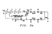
Fig. 3a illustrates an improved implementation of the disclosure applied for example to a LDO. -
Fig. 3b illustrates details of the connection of a small resistor, as shown inFig. 4a , to the fast feedback pad including bond wires and parasitic resistances in the fast feedback loop according to a key point of the present disclosure. -
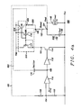
Fig. 4a shows a stabilization circuit as disclosed in the patent application serial number13/066,598 -
Fig. 4b shows in more details the connections ofFig. 4a with all parasitic components and bond wires. The metallization resistance of a pass resistor is here in series with a small resistor and is hence not included in the fast loop. -
Fig. 4c shows again in more details the connections ofFig. 4a with all parasitic components and bond wires. In this embodiment the metallization resistance Rmet of the pass resistor is here not in series with the small resistor is hence included in the fast loop. -
Fig. 5 shows a plot of a LDO response to a load transient from 1 mA to 300mA according to the circuit design shown inFig. 3 b. -
Fig. 6 illustrates a flowchart of a method to improve dynamic load transient performance of circuits supplying high current such as LDOs, amplifiers, or buffers. - Methods and circuits to improve dynamic load transient performance of circuits supplying high currents such as LDOs, amplifiers, or buffers by overcoming degradations caused by voltage drops due to resistances of bond wires, metallization of pass device, and substrate routing are disclosed.
-
Fig. 1 shows the basic elements of a first implementation of a circuit using two bond wires including resistances of bond wires, metallization, and substrate routings. - The circuit of
Fig. 1 illustrates resistances of passdevice metallization Rmet 1,Rbond 2 of the two bond wires, and substrate routings Rsub 3. Actually the circuit ofFig.1 shows Rbond<x:0>, which means "x" bond wires in parallel. FurthermoreFig. 1 shows two pads P1/ P3 and two bond fingers P2/ P4, an external capacitor Cext, and a feedback loop 4 for fast load transient. Moreover the exemplary circuit ofFig. 1 shows an LDO having a voltage divider R1/R2 providing feedback to adifferential amplifier 5, receiving a reference voltage Vref as a second input, a number ofbuffer amplifier stages pass device 8. The fast loop is sensed at Rmet+. - Using one bond wire instead of two bond wires for supplying of e.g. 300mA, compared to supplying 150mA in previous connection would double the voltage drop in bond wires, and double the contributions in voltage drop due to increase in the metallization resistance ( as the pass device size has doubled).
- The disadvantage of the implementation shown in
Fig.1 when one bond wire is used is a low dynamic load transient performance of e.g. a LDO due to parasitic contributions due to: - bond wire voltage drop;
- Metallization resistance of pass device; and
- Substrate routing.
-
Fig. 2 shows a plot of a LDO response to a load transient from 1mA to 300mA according to the circuit design shown inFig. 1 , wherein one bond wire is used. - The dip in the
output voltage 20 to the load transient 21 from 1 mA to 300mA is 84 mV. Such a dip is an impediment for many applications. -
Fig. 3a illustrates an improved implementation of the disclosure applied for example to a LDO again. This implementation is characterized by including the parasitics, caused by resistances of bond wires, metallization and substrate routings, in the fast regulation loop. - The objective of the circuit of
Fig. 3a is to improve the dynamic load transient performance of a circuit supplying high currents, e.g. a LDO, by avoiding parasitic contributions due to resistances of bond wire, metallization of pass device, and substrate routing and using one bond wire. - The circuit of
Fig. 3a has only resistance Rbond between P1 and P2, illustrating use of one bond wire only. For this implementation a stabilization circuit, as e.g. disclosed in European patent application11368014.4 Fig. 4a shows this stabilization circuit as disclosed in the patent application serial number11368014.4 - The stabilization circuit of
Fig. 4a shows an additional pass device in parallel with the main pass device. Thisadditional pass device 218 would have typically about 5% of the existing 100% channel width of the main pass118 device, butpass device 218 may range from between about 1 to 10% but preferably ranges from between about 0.5 to 15% of the existing channel width of the main pass device. Theadditional pass device 218 will share the power connection and the gate connection. However, between the drain and the output of the LDO aresistor 220 of typically about 2Ω is deployed which may range from between about 1 to 5Ω but preferably ranges from between about 0.5 to 10Ω. The Miller capacitor is now connected to the drain of this new pass device. This means the Miller capacitor sees a much greater ESR, and so it amplifies the fast feedback loop gain, moving the zero node back within the bandwidth. Themain pass device 118 still has low ESR, and so the drop-out performance remains unchanged. In this case the phase-margin now exceeds the previous 100mΩ ESR environment. - Again referring to
Fig. 4a , acurrent mirror stage 216 uses a third and smaller currentmirror PMOS transistor 218 as additional pass device. Furthermore the drain ofadditional pass device 218 is coupled vianode 262 to asmall resistor 220 which in turn is coupled tooutput node 162. A newfast feedback loop 282 is coupled fromnode 262 via capacitor (Cmiller) 115 tonode 160, the input to buffer 112. - It should be noted that
device 220 which is connected inFig. 4a tonode 162 should be connected such that it includes as many parasitics (e.g. Rmet, Rbond, and Rsub) as possible within the fast feedback loop. Hence it is especially preferred to connectdevice 220 to VFB node as shown inFig. 3 b. -
Fig. 4b shows in more details the connections ofFig. 4a with all parasitic components and bond wires. The metallization resistance Rmet ofpass resistor 118 is here in series withresistor 220 and is hence not included in the fast loop. -
Fig. 4c shows again in more details the connections ofFig. 4a with all parasitic components and bond wires. In this embodiment the metallization resistance Rmet ofpass resistor 118 is here not in series withresistor 220 is hence included in thefast loop 40. - Returning to
Fig. 3a the essential features of the new implementation disclosed shown with the example of a LDO are: - Separate pad for feedback (Rbond is connected to node VFB (feedback voltage);
- Separate loop for fast loop response of LDO including parasitics; and
- Stabilizing circuit within said fast regulation loop
-
Fig. 3b illustrates details of the connection of thesmall resistor 220, as shown inFig. 4a , to the fast feedback pad including bond wires and parasitic resistances in the fast feedback loop according to a key point of the present disclosure. This would improve the load transient as all the parasitic components are included in the fast loop. - It should be noted that the circuits disclosed are applicable to any numbers of bond wires.
-
Fig. 5 shows a plot of a LDO response to a load transient from 1 mA to 300mA according to the circuit design shown inFig. 3 b. Implementing the modifications of the circuit shown inFig. 3b results in an improvement of 50 mV or 60% compared to the plot ofFig. 2 , showing a transient response of 84 mV. The dip in theoutput voltage 50 to the load transient 51 shown inFig. 5 from 1 mA to 300mA is 38.8 mV. -
Fig. 6 illustrates a flowchart of a method t to improve dynamic load transient performance of circuits supplying high current such as LDOs, amplifiers, or buffers. -
Step 60 of the method ofFig. 6 illustrates the provision of a circuit as e.g. a LDO, buffer, or amplifier supplying high currents and having parasitic resistances caused by bond wires, metallization of pass devices, and substrate routings.Step 61 depicts including parasitic resistances in a separate loop for fast loop response. Step 32 illustrates implementing stabilizing circuit within said fast loop response. Step 33 shows deploying separate pad for the fast loop response connected to feedback voltage VFB. - While the disclosure has been particularly shown and described with reference to the preferred embodiments thereof, it will be understood by those skilled in the art that various changes in form and details may be made without departing from the spirit and scope of the disclosure.
Claims (15)
- A method to improve dynamic load transient performance of circuits supplying high current, comprising the following steps:(1) providing an electronic circuit supplying high currents and having parasitic resistances;(2) including parasitic resistances in a separate loop for fast loop response;(3) implementing stabilizing circuit within said fast loop response; and(4) deploying separate pad for the fast loop response connected to feedback voltage VFB.
- The method of claim 1 wherein said high current comprise a range of more than 200mA.
- The method of claim 1 wherein said circuit is either a LDO, an amplifier, or a buffer.
- The method of claim 1 wherein said stabilization circuit is achieved by splitting a main pass device into two unequal parts, by placing a controlled impedance in series with a smaller part of the pass device, and taking the fast feedback loop from a node between the pass device and the controlled impedance and coupling it back to a Miller capacitor.
- The method of claim 1 wherein said parasitic resistances comprise resistances of one or more bond wires, metallization of one or more pass devices, and substrate routings.
- The method of claim 1 wherein the resistance of a main pass transistor is not included in the loop of fast response.
- The method of claim 1 wherein one bond wire or more than one bond wire are used.
- A circuit to improve dynamic load transient performance of circuits supplying high current and having parasitic resistances, comprising:- a separate loop for fast transient response including the parasitic resistances;- a separate pad for the loop for fast transient response; and- a stabilizing circuit connected to said loop for fast transient response.
- The circuit of claim 8 wherein said circuit is either an LDO, or an amplifier, or a buffer.
- The circuit of claim 8 wherein said parasitic resistances comprise resistances of one or more bond wires, metallization of one or more pass devices, and substrate routings
- The circuit of claim 8 wherein the circuit comprises one bond wire, or more than one bond wire.
- The circuit of claim 8 wherein said high current comprise a range of more than 200mA.
- The circuit of claim 8 wherein said loop for fast transient response comprises a capacitor.
- The circuit of claim 8 wherein the stabilizing circuit comprises a main pass transistor and an additional pass transistor in parallel to the main pass transistor.
- The circuit of claim 14 wherein a resistive device, e.g. a resistor, having a resistance in a range between about 0.5 to 10Ω, is deployed a drain of the additional pass transistor and an output of the circuit.
Applications Claiming Priority (1)
| Application Number | Priority Date | Filing Date | Title |
|---|---|---|---|
| US13/652,996 US9239585B2 (en) | 2012-10-16 | 2012-10-16 | Load transient, reduced bond wires for circuits supplying large currents |
Publications (3)
| Publication Number | Publication Date |
|---|---|
| EP2755103A2 true EP2755103A2 (en) | 2014-07-16 |
| EP2755103A3 EP2755103A3 (en) | 2018-01-10 |
| EP2755103B1 EP2755103B1 (en) | 2021-04-28 |
Family
ID=47563146
Family Applications (1)
| Application Number | Title | Priority Date | Filing Date |
|---|---|---|---|
| EP12392003.5A Active EP2755103B1 (en) | 2012-10-16 | 2012-11-14 | Improved load transient, reduced bond wires for circuits supplying large currents |
Country Status (2)
| Country | Link |
|---|---|
| US (2) | US9239585B2 (en) |
| EP (1) | EP2755103B1 (en) |
Families Citing this family (5)
| Publication number | Priority date | Publication date | Assignee | Title |
|---|---|---|---|---|
| US8866553B2 (en) * | 2013-03-14 | 2014-10-21 | Linear Technology Corporation | Output stage with fast feedback for driving ADC |
| US10185339B2 (en) * | 2013-09-18 | 2019-01-22 | Texas Instruments Incorporated | Feedforward cancellation of power supply noise in a voltage regulator |
| CN106774580B (en) * | 2017-01-19 | 2018-06-22 | 武汉众为信息技术有限公司 | A kind of LDO circuit of fast transient response high PSRR |
| CN110727308B (en) * | 2019-11-21 | 2020-10-02 | 华大半导体有限公司 | Auxiliary circuit suitable for no off-chip capacitance type voltage regulator |
| US12045073B2 (en) * | 2021-05-03 | 2024-07-23 | Ningbo Aura Semiconductor Co., Limited | Enabling fast transient response in a linear regulator when loop-gain reduction is employed for frequency compensation |
Family Cites Families (7)
| Publication number | Priority date | Publication date | Assignee | Title |
|---|---|---|---|---|
| GB2356991B (en) * | 1999-12-02 | 2003-10-22 | Zetex Plc | A negative feedback amplifier circuit |
| EP1378808B1 (en) * | 2002-07-05 | 2008-02-20 | Dialog Semiconductor GmbH | LDO regulator with wide output load range and fast internal loop |
| US20060273771A1 (en) * | 2005-06-03 | 2006-12-07 | Micrel, Incorporated | Creating additional phase margin in the open loop gain of a negative feedback amplifier system |
| US7129686B1 (en) | 2005-08-03 | 2006-10-31 | National Semiconductor Corporation | Apparatus and method for a high PSRR LDO regulator |
| US8129962B2 (en) | 2008-08-15 | 2012-03-06 | Texas Instruments Incorporated | Low dropout voltage regulator with clamping |
| US8378652B2 (en) | 2008-12-23 | 2013-02-19 | Texas Instruments Incorporated | Load transient response time of LDOs with NMOS outputs with a voltage controlled current source |
| EP2541363B1 (en) | 2011-04-13 | 2014-05-14 | Dialog Semiconductor GmbH | LDO with improved stability |
-
2012
- 2012-10-16 US US13/652,996 patent/US9239585B2/en active Active
- 2012-11-14 EP EP12392003.5A patent/EP2755103B1/en active Active
-
2016
- 2016-01-15 US US14/996,705 patent/US9454170B2/en active Active
Also Published As
| Publication number | Publication date |
|---|---|
| US9239585B2 (en) | 2016-01-19 |
| US20140103893A1 (en) | 2014-04-17 |
| EP2755103B1 (en) | 2021-04-28 |
| US9454170B2 (en) | 2016-09-27 |
| US20160132064A1 (en) | 2016-05-12 |
| EP2755103A3 (en) | 2018-01-10 |
Similar Documents
| Publication | Publication Date | Title |
|---|---|---|
| EP2846213B1 (en) | Method and apparatus for limiting startup inrush current for low dropout regulator | |
| CN106444954B (en) | Voltage stabilizer | |
| TWI546642B (en) | Two-stage low-dropout linear power supply systems and methods | |
| US8912772B2 (en) | LDO with improved stability | |
| CN112578842B (en) | Low dropout voltage regulator with improved power supply rejection | |
| TWI696910B (en) | Low drop-out voltage regulator circuit and voltage regulating method thereof | |
| US9122293B2 (en) | Method and apparatus for LDO and distributed LDO transient response accelerator | |
| US9454170B2 (en) | Load transient, reduced bond wires for circuits supplying large currents | |
| US8878510B2 (en) | Reducing power consumption in a voltage regulator | |
| US9927828B2 (en) | System and method for a linear voltage regulator | |
| CN110231851B (en) | Output voltage compensation circuit, method, voltage regulator circuit and display device | |
| US9360876B2 (en) | Voltage supply circuit having an absorption unit and method for operating the same | |
| JP2018517991A (en) | Voltage regulator | |
| TW201028814A (en) | Method for improving power-supply rejection | |
| KR20150024272A (en) | Voltage regulator | |
| US8085006B2 (en) | Shunt regulator | |
| US20140312864A1 (en) | Light load stability circuitry for ldo regulator | |
| KR101592500B1 (en) | Low drop out regulator | |
| TWI774491B (en) | Voltage regulator device | |
| KR20160012858A (en) | Low dropout regulator | |
| CN112486239B (en) | Low dropout regulator circuit | |
| US20190384344A1 (en) | Circuit for Generating a Negative Higher Order Temperature Coefficient Current | |
| Valle-Mayorga et al. | Back to the Future: An All-NMOS SiC Linear Voltage Regulator for High Temperature Applications | |
| CN115705068A (en) | voltage regulator |
Legal Events
| Date | Code | Title | Description |
|---|---|---|---|
| PUAI | Public reference made under article 153(3) epc to a published international application that has entered the european phase |
Free format text: ORIGINAL CODE: 0009012 |
|
| 17P | Request for examination filed |
Effective date: 20121114 |
|
| AK | Designated contracting states |
Kind code of ref document: A2 Designated state(s): AL AT BE BG CH CY CZ DE DK EE ES FI FR GB GR HR HU IE IS IT LI LT LU LV MC MK MT NL NO PL PT RO RS SE SI SK SM TR |
|
| AX | Request for extension of the european patent |
Extension state: BA ME |
|
| PUAL | Search report despatched |
Free format text: ORIGINAL CODE: 0009013 |
|
| AK | Designated contracting states |
Kind code of ref document: A3 Designated state(s): AL AT BE BG CH CY CZ DE DK EE ES FI FR GB GR HR HU IE IS IT LI LT LU LV MC MK MT NL NO PL PT RO RS SE SI SK SM TR |
|
| AX | Request for extension of the european patent |
Extension state: BA ME |
|
| RIC1 | Information provided on ipc code assigned before grant |
Ipc: G05F 1/10 20060101ALI20171206BHEP Ipc: G05F 1/575 20060101AFI20171206BHEP |
|
| STAA | Information on the status of an ep patent application or granted ep patent |
Free format text: STATUS: REQUEST FOR EXAMINATION WAS MADE |
|
| R17P | Request for examination filed (corrected) |
Effective date: 20180710 |
|
| RBV | Designated contracting states (corrected) |
Designated state(s): AL AT BE BG CH CY CZ DE DK EE ES FI FR GB GR HR HU IE IS IT LI LT LU LV MC MK MT NL NO PL PT RO RS SE SI SK SM TR |
|
| STAA | Information on the status of an ep patent application or granted ep patent |
Free format text: STATUS: EXAMINATION IS IN PROGRESS |
|
| 17Q | First examination report despatched |
Effective date: 20190403 |
|
| GRAP | Despatch of communication of intention to grant a patent |
Free format text: ORIGINAL CODE: EPIDOSNIGR1 |
|
| STAA | Information on the status of an ep patent application or granted ep patent |
Free format text: STATUS: GRANT OF PATENT IS INTENDED |
|
| INTG | Intention to grant announced |
Effective date: 20201202 |
|
| GRAS | Grant fee paid |
Free format text: ORIGINAL CODE: EPIDOSNIGR3 |
|
| GRAA | (expected) grant |
Free format text: ORIGINAL CODE: 0009210 |
|
| STAA | Information on the status of an ep patent application or granted ep patent |
Free format text: STATUS: THE PATENT HAS BEEN GRANTED |
|
| AK | Designated contracting states |
Kind code of ref document: B1 Designated state(s): AL AT BE BG CH CY CZ DE DK EE ES FI FR GB GR HR HU IE IS IT LI LT LU LV MC MK MT NL NO PL PT RO RS SE SI SK SM TR |
|
| REG | Reference to a national code |
Ref country code: GB Ref legal event code: FG4D |
|
| REG | Reference to a national code |
Ref country code: CH Ref legal event code: EP |
|
| REG | Reference to a national code |
Ref country code: AT Ref legal event code: REF Ref document number: 1387811 Country of ref document: AT Kind code of ref document: T Effective date: 20210515 |
|
| REG | Reference to a national code |
Ref country code: DE Ref legal event code: R096 Ref document number: 602012075373 Country of ref document: DE |
|
| REG | Reference to a national code |
Ref country code: IE Ref legal event code: FG4D |
|
| REG | Reference to a national code |
Ref country code: LT Ref legal event code: MG9D |
|
| REG | Reference to a national code |
Ref country code: AT Ref legal event code: MK05 Ref document number: 1387811 Country of ref document: AT Kind code of ref document: T Effective date: 20210428 |
|
| PG25 | Lapsed in a contracting state [announced via postgrant information from national office to epo] |
Ref country code: FI Free format text: LAPSE BECAUSE OF FAILURE TO SUBMIT A TRANSLATION OF THE DESCRIPTION OR TO PAY THE FEE WITHIN THE PRESCRIBED TIME-LIMIT Effective date: 20210428 Ref country code: NL Free format text: LAPSE BECAUSE OF FAILURE TO SUBMIT A TRANSLATION OF THE DESCRIPTION OR TO PAY THE FEE WITHIN THE PRESCRIBED TIME-LIMIT Effective date: 20210428 Ref country code: LT Free format text: LAPSE BECAUSE OF FAILURE TO SUBMIT A TRANSLATION OF THE DESCRIPTION OR TO PAY THE FEE WITHIN THE PRESCRIBED TIME-LIMIT Effective date: 20210428 Ref country code: AT Free format text: LAPSE BECAUSE OF FAILURE TO SUBMIT A TRANSLATION OF THE DESCRIPTION OR TO PAY THE FEE WITHIN THE PRESCRIBED TIME-LIMIT Effective date: 20210428 Ref country code: BG Free format text: LAPSE BECAUSE OF FAILURE TO SUBMIT A TRANSLATION OF THE DESCRIPTION OR TO PAY THE FEE WITHIN THE PRESCRIBED TIME-LIMIT Effective date: 20210728 Ref country code: HR Free format text: LAPSE BECAUSE OF FAILURE TO SUBMIT A TRANSLATION OF THE DESCRIPTION OR TO PAY THE FEE WITHIN THE PRESCRIBED TIME-LIMIT Effective date: 20210428 |
|
| PG25 | Lapsed in a contracting state [announced via postgrant information from national office to epo] |
Ref country code: SE Free format text: LAPSE BECAUSE OF FAILURE TO SUBMIT A TRANSLATION OF THE DESCRIPTION OR TO PAY THE FEE WITHIN THE PRESCRIBED TIME-LIMIT Effective date: 20210428 Ref country code: RS Free format text: LAPSE BECAUSE OF FAILURE TO SUBMIT A TRANSLATION OF THE DESCRIPTION OR TO PAY THE FEE WITHIN THE PRESCRIBED TIME-LIMIT Effective date: 20210428 Ref country code: LV Free format text: LAPSE BECAUSE OF FAILURE TO SUBMIT A TRANSLATION OF THE DESCRIPTION OR TO PAY THE FEE WITHIN THE PRESCRIBED TIME-LIMIT Effective date: 20210428 Ref country code: GR Free format text: LAPSE BECAUSE OF FAILURE TO SUBMIT A TRANSLATION OF THE DESCRIPTION OR TO PAY THE FEE WITHIN THE PRESCRIBED TIME-LIMIT Effective date: 20210729 Ref country code: IS Free format text: LAPSE BECAUSE OF FAILURE TO SUBMIT A TRANSLATION OF THE DESCRIPTION OR TO PAY THE FEE WITHIN THE PRESCRIBED TIME-LIMIT Effective date: 20210828 Ref country code: PT Free format text: LAPSE BECAUSE OF FAILURE TO SUBMIT A TRANSLATION OF THE DESCRIPTION OR TO PAY THE FEE WITHIN THE PRESCRIBED TIME-LIMIT Effective date: 20210830 Ref country code: PL Free format text: LAPSE BECAUSE OF FAILURE TO SUBMIT A TRANSLATION OF THE DESCRIPTION OR TO PAY THE FEE WITHIN THE PRESCRIBED TIME-LIMIT Effective date: 20210428 Ref country code: NO Free format text: LAPSE BECAUSE OF FAILURE TO SUBMIT A TRANSLATION OF THE DESCRIPTION OR TO PAY THE FEE WITHIN THE PRESCRIBED TIME-LIMIT Effective date: 20210728 Ref country code: ES Free format text: LAPSE BECAUSE OF FAILURE TO SUBMIT A TRANSLATION OF THE DESCRIPTION OR TO PAY THE FEE WITHIN THE PRESCRIBED TIME-LIMIT Effective date: 20210428 |
|
| REG | Reference to a national code |
Ref country code: NL Ref legal event code: MP Effective date: 20210428 |
|
| PG25 | Lapsed in a contracting state [announced via postgrant information from national office to epo] |
Ref country code: SM Free format text: LAPSE BECAUSE OF FAILURE TO SUBMIT A TRANSLATION OF THE DESCRIPTION OR TO PAY THE FEE WITHIN THE PRESCRIBED TIME-LIMIT Effective date: 20210428 Ref country code: SK Free format text: LAPSE BECAUSE OF FAILURE TO SUBMIT A TRANSLATION OF THE DESCRIPTION OR TO PAY THE FEE WITHIN THE PRESCRIBED TIME-LIMIT Effective date: 20210428 Ref country code: EE Free format text: LAPSE BECAUSE OF FAILURE TO SUBMIT A TRANSLATION OF THE DESCRIPTION OR TO PAY THE FEE WITHIN THE PRESCRIBED TIME-LIMIT Effective date: 20210428 Ref country code: CZ Free format text: LAPSE BECAUSE OF FAILURE TO SUBMIT A TRANSLATION OF THE DESCRIPTION OR TO PAY THE FEE WITHIN THE PRESCRIBED TIME-LIMIT Effective date: 20210428 Ref country code: DK Free format text: LAPSE BECAUSE OF FAILURE TO SUBMIT A TRANSLATION OF THE DESCRIPTION OR TO PAY THE FEE WITHIN THE PRESCRIBED TIME-LIMIT Effective date: 20210428 Ref country code: RO Free format text: LAPSE BECAUSE OF FAILURE TO SUBMIT A TRANSLATION OF THE DESCRIPTION OR TO PAY THE FEE WITHIN THE PRESCRIBED TIME-LIMIT Effective date: 20210428 |
|
| REG | Reference to a national code |
Ref country code: DE Ref legal event code: R097 Ref document number: 602012075373 Country of ref document: DE |
|
| PLBE | No opposition filed within time limit |
Free format text: ORIGINAL CODE: 0009261 |
|
| STAA | Information on the status of an ep patent application or granted ep patent |
Free format text: STATUS: NO OPPOSITION FILED WITHIN TIME LIMIT |
|
| 26N | No opposition filed |
Effective date: 20220131 |
|
| PG25 | Lapsed in a contracting state [announced via postgrant information from national office to epo] |
Ref country code: IS Free format text: LAPSE BECAUSE OF FAILURE TO SUBMIT A TRANSLATION OF THE DESCRIPTION OR TO PAY THE FEE WITHIN THE PRESCRIBED TIME-LIMIT Effective date: 20210828 Ref country code: AL Free format text: LAPSE BECAUSE OF FAILURE TO SUBMIT A TRANSLATION OF THE DESCRIPTION OR TO PAY THE FEE WITHIN THE PRESCRIBED TIME-LIMIT Effective date: 20210428 |
|
| PG25 | Lapsed in a contracting state [announced via postgrant information from national office to epo] |
Ref country code: MC Free format text: LAPSE BECAUSE OF FAILURE TO SUBMIT A TRANSLATION OF THE DESCRIPTION OR TO PAY THE FEE WITHIN THE PRESCRIBED TIME-LIMIT Effective date: 20210428 |
|
| REG | Reference to a national code |
Ref country code: CH Ref legal event code: PL |
|
| PG25 | Lapsed in a contracting state [announced via postgrant information from national office to epo] |
Ref country code: LU Free format text: LAPSE BECAUSE OF NON-PAYMENT OF DUE FEES Effective date: 20211114 Ref country code: IT Free format text: LAPSE BECAUSE OF FAILURE TO SUBMIT A TRANSLATION OF THE DESCRIPTION OR TO PAY THE FEE WITHIN THE PRESCRIBED TIME-LIMIT Effective date: 20210428 Ref country code: BE Free format text: LAPSE BECAUSE OF NON-PAYMENT OF DUE FEES Effective date: 20211130 |
|
| REG | Reference to a national code |
Ref country code: BE Ref legal event code: MM Effective date: 20211130 |
|
| PG25 | Lapsed in a contracting state [announced via postgrant information from national office to epo] |
Ref country code: IE Free format text: LAPSE BECAUSE OF NON-PAYMENT OF DUE FEES Effective date: 20211114 |
|
| PG25 | Lapsed in a contracting state [announced via postgrant information from national office to epo] |
Ref country code: FR Free format text: LAPSE BECAUSE OF NON-PAYMENT OF DUE FEES Effective date: 20211130 |
|
| PG25 | Lapsed in a contracting state [announced via postgrant information from national office to epo] |
Ref country code: HU Free format text: LAPSE BECAUSE OF FAILURE TO SUBMIT A TRANSLATION OF THE DESCRIPTION OR TO PAY THE FEE WITHIN THE PRESCRIBED TIME-LIMIT; INVALID AB INITIO Effective date: 20121114 Ref country code: CY Free format text: LAPSE BECAUSE OF FAILURE TO SUBMIT A TRANSLATION OF THE DESCRIPTION OR TO PAY THE FEE WITHIN THE PRESCRIBED TIME-LIMIT Effective date: 20210428 |
|
| PG25 | Lapsed in a contracting state [announced via postgrant information from national office to epo] |
Ref country code: LI Free format text: LAPSE BECAUSE OF NON-PAYMENT OF DUE FEES Effective date: 20220701 Ref country code: CH Free format text: LAPSE BECAUSE OF NON-PAYMENT OF DUE FEES Effective date: 20220701 |
|
| PG25 | Lapsed in a contracting state [announced via postgrant information from national office to epo] |
Ref country code: MK Free format text: LAPSE BECAUSE OF FAILURE TO SUBMIT A TRANSLATION OF THE DESCRIPTION OR TO PAY THE FEE WITHIN THE PRESCRIBED TIME-LIMIT Effective date: 20210428 |
|
| PG25 | Lapsed in a contracting state [announced via postgrant information from national office to epo] |
Ref country code: TR Free format text: LAPSE BECAUSE OF FAILURE TO SUBMIT A TRANSLATION OF THE DESCRIPTION OR TO PAY THE FEE WITHIN THE PRESCRIBED TIME-LIMIT Effective date: 20210428 |
|
| PG25 | Lapsed in a contracting state [announced via postgrant information from national office to epo] |
Ref country code: MT Free format text: LAPSE BECAUSE OF FAILURE TO SUBMIT A TRANSLATION OF THE DESCRIPTION OR TO PAY THE FEE WITHIN THE PRESCRIBED TIME-LIMIT Effective date: 20210428 |
|
| PGFP | Annual fee paid to national office [announced via postgrant information from national office to epo] |
Ref country code: DE Payment date: 20251103 Year of fee payment: 14 |
|
| PGFP | Annual fee paid to national office [announced via postgrant information from national office to epo] |
Ref country code: GB Payment date: 20251110 Year of fee payment: 14 |