EP2753039A1 - System and method for processing data flows - Google Patents
System and method for processing data flows Download PDFInfo
- Publication number
- EP2753039A1 EP2753039A1 EP13150356.7A EP13150356A EP2753039A1 EP 2753039 A1 EP2753039 A1 EP 2753039A1 EP 13150356 A EP13150356 A EP 13150356A EP 2753039 A1 EP2753039 A1 EP 2753039A1
- Authority
- EP
- European Patent Office
- Prior art keywords
- data
- framer
- sampling rate
- memory access
- direct memory
- Prior art date
- Legal status (The legal status is an assumption and is not a legal conclusion. Google has not performed a legal analysis and makes no representation as to the accuracy of the status listed.)
- Granted
Links
- 238000012545 processing Methods 0.000 title claims abstract description 28
- 238000000034 method Methods 0.000 title claims description 19
- 238000005070 sampling Methods 0.000 claims abstract description 73
- 230000015654 memory Effects 0.000 claims abstract description 70
- 239000000969 carrier Substances 0.000 claims abstract description 9
- 238000012546 transfer Methods 0.000 claims description 30
- 230000005540 biological transmission Effects 0.000 claims description 12
- 238000004590 computer program Methods 0.000 claims description 9
- 230000009977 dual effect Effects 0.000 claims description 6
- 238000004891 communication Methods 0.000 description 11
- 230000006870 function Effects 0.000 description 9
- 238000010586 diagram Methods 0.000 description 7
- 238000005111 flow chemistry technique Methods 0.000 description 6
- 238000003860 storage Methods 0.000 description 6
- 238000006243 chemical reaction Methods 0.000 description 5
- 230000003321 amplification Effects 0.000 description 3
- 238000001914 filtration Methods 0.000 description 3
- 238000007726 management method Methods 0.000 description 3
- 230000000873 masking effect Effects 0.000 description 3
- 238000012986 modification Methods 0.000 description 3
- 230000004048 modification Effects 0.000 description 3
- 238000003199 nucleic acid amplification method Methods 0.000 description 3
- 230000003287 optical effect Effects 0.000 description 3
- 230000008569 process Effects 0.000 description 3
- 238000003892 spreading Methods 0.000 description 3
- 230000002457 bidirectional effect Effects 0.000 description 2
- 239000000872 buffer Substances 0.000 description 2
- 230000010267 cellular communication Effects 0.000 description 2
- 239000004065 semiconductor Substances 0.000 description 2
- 230000007480 spreading Effects 0.000 description 2
- 230000026676 system process Effects 0.000 description 2
- 230000008901 benefit Effects 0.000 description 1
- 238000000354 decomposition reaction Methods 0.000 description 1
- 230000001419 dependent effect Effects 0.000 description 1
- 238000001514 detection method Methods 0.000 description 1
- 238000009826 distribution Methods 0.000 description 1
- 230000000694 effects Effects 0.000 description 1
- 230000005294 ferromagnetic effect Effects 0.000 description 1
- 230000007274 generation of a signal involved in cell-cell signaling Effects 0.000 description 1
- 230000010365 information processing Effects 0.000 description 1
- 230000007774 longterm Effects 0.000 description 1
- 230000005291 magnetic effect Effects 0.000 description 1
- 238000005259 measurement Methods 0.000 description 1
- 230000005055 memory storage Effects 0.000 description 1
- 238000012913 prioritisation Methods 0.000 description 1
- 238000009877 rendering Methods 0.000 description 1
- 230000011664 signaling Effects 0.000 description 1
- 230000006641 stabilisation Effects 0.000 description 1
- 238000011105 stabilization Methods 0.000 description 1
- 230000002123 temporal effect Effects 0.000 description 1
Images


Classifications
-
- H—ELECTRICITY
- H04—ELECTRIC COMMUNICATION TECHNIQUE
- H04L—TRANSMISSION OF DIGITAL INFORMATION, e.g. TELEGRAPHIC COMMUNICATION
- H04L27/00—Modulated-carrier systems
- H04L27/26—Systems using multi-frequency codes
- H04L27/2601—Multicarrier modulation systems
- H04L27/2647—Arrangements specific to the receiver only
Definitions
- This invention relates to a system and method for processing data flows and particularly, though not exclusively, to such a system and method for processing flow of data in cellular communications networks.
- wireless user equipment units for example, mobile phones
- a radio access network covers a geographical area which is divided into cells, with each cell area being served by a radio base station.
- Several base stations are connected, typically via land lines, to a control node known as a radio network controller (RNC).
- RNC radio network controller
- Such a control node supervises and coordinates various activities of the several radio base stations which are connected to it.
- the radio network controllers are typically connected to one or more core networks.
- UMTS Universal Mobile Telecommunications
- UTRAN Universal Mobile Telecommunications Terrestrial Radio Access Network
- the UMTS is a third generation (3G) system and UTRAN is essentially a radio access network providing wideband code division multiple access (WCDMA) to user equipment units.
- WCDMA wideband code division multiple access
- Fourth generation systems are evolving towards a broadband and mobile system.
- the 3rd Generation Partnership Project has proposed a Long Term Evolution (LTE) solution, namely, an Evolved Universal Mobile Telecommunication System Territorial Radio Access Network, (E-UTRAN), for a mobile access network.
- LTE Long Term Evolution
- E-UTRAN Evolved Universal Mobile Telecommunication System Territorial Radio Access Network
- a radio base station In many radio access networks the radio base station is a concentrated node with most of its components being located at a concentrated site. However, a radio base station can also be configured with a more distributed architecture.
- a distributed radio base station can take the form of one or more radio equipment (RE) portions that are linked to a radio equipment control (REC) portion over an internal interface.
- RE radio equipment
- REC radio equipment control
- An internal interface of a radio base station which links a radio equipment portion of the radio base station to a radio equipment control portion of the base station is the Common Public Radio Interface (CPRI).
- CPRI Common Public Radio Interface
- the Common Public Radio Interface (CPRI) is described in Common Public Radio Interface (CPRI) Interface Specification Version 4.1 (18 February 2009) and also Version 4.2 (2010) and Version 5(2011).
- the Common Public Radio Interface is an industry cooperation aimed at defining a publicly available specification for the key internal interface of radio base stations between radio equipment control (REC) and radio equipment (RE), thereby allowing base station manufacturers to share a common protocol and more easily adapt platforms from one customer to another.
- a radio base station is decomposed into two separate blocks, known as REC and RE.
- the REC provides access to a UMTS network, for example, via the lub interface, whereas the RE serves as the air interface to user equipment, known as Uu in a UMTS network.
- the REC generally comprises the radio functions of the digital baseband domain, whereas the RE contains analogue radio frequency functions.
- the functional split between the REC and RE is done in such a way that a generic interface, CPRI, based on In-Phase and Quadrature (IQ) data can be defined.
- CPRI In-Phase and Quadrature
- IQ data flows can be sent over one physical link with each data flow reflecting the data of one antenna for one carrier, the so-called antenna carrier "AxC.”
- AxC antenna carrier
- AxC's having the same sampling rate may be aggregated into an "AxC Group.”
- IQ data of different antennas along with control data are multiplexed onto a transmission line.
- the CPRI has a basic frame structure for carrying a control word and an IQ data block.
- the functional split between the REC and RE allows the RE to be positioned close to an associated antenna. This reduces the distance which the associated signals have to travel before they are received by the RE, thereby negating the need for tower-mounted amplifiers and antenna system controllers.
- the link between the RE and REC is generally optical, allowing the link length to be much greater when compared with wired coaxial systems. Therefore, the distance between the RE and RRC can be around10Km, thereby increasing the flexibility of deployment of RE's within the network when utilising CPRI.
- One REC may be linked to two or more RE's or one RE may be linked to multiple REC's in a chain topology with each REC being configured to forward data to other REC's in the chain.
- This Digital Signal Processor includes (inter alia) a CPRI unit which includes a "framer" module which handles the transmission and reception of all IQ data, and a DMA (direct memory access) module associated with the framer which transfers the receive and transmit IQ data to and from antenna carrier buffers in a memory.
- FIG. 1 shows an example of this known solution.
- a first framer 101 receives RF data (from an RE 102 for example) and its associated DMA module 103 transfers data with a first sampling rate to system memory 104.
- a second framer 105 receives the RF data from the first framer 101 via auxiliary interface modules 106, 107 and outputs it directly via Serialiser/Deserialiser links 108, 109 to a third framer 110.
- a DMA module 111 associated with the third framer 110 transfers data with a second sampling rate to system memory 112.
- the DMA module 103 associated with the first framer 101 fetches data with the first sampling rate from system memory 104 and transfers it to the first framer 101 for outputting towards the RE 102.
- the third framer's DMA module 111 fetches data with the second sampling rate from system memory 112 and the third framer 110 transfers the data to the second framer 105 via the serialiser/deserialiser 108, 109 interface.
- the second framer 105 transfers the data with the second sampling rate via the auxiliary interfaces 107, 106 to the first framer 101 which, in turn, outputs the data towards the RE 102.
- Each CPRI unit contains receive and transmit configuration tables that determine which AxC's in a frame to transfer to or fetch from system memory and their location in the frame. Further, each CPRI unit contains receive mask registers (not shown) with the masking of bits of the auxiliary interface 106, 107. For example, if a masking bit is "set” then data coming from framer2 105 is sent to the RE 102. Conversely, if the masking bit is "cleared” then the data read by framer1 101 from system memory 104 is sent to the RE 102.
- This solution has the disadvantage of requiring an extra CPRI unit and interconnections.
- the present invention provides a system and method for processing data flows as described in the accompanying claims.
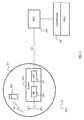
- FIG.2 an example of part of a wireless communication system operating in accordance with embodiments of the invention is illustrated and indicated generally at 200 and comprises a 3G macro cell whose coverage area is indicated at 201.
- a core network 202 of the wireless communication system of FIG.2 which includes a Mobile Switching Centre (MSC) and other network elements (not shown), may serve to interface the wireless communication system 200 with a packet data network, for example a Public Switched Data Network (PSDN), (such as the internet) or a Public Switched Telephone Network (PSTN).
- PSDN Public Switched Data Network
- PSTN Public Switched Telephone Network
- the 3G macro-cell 201 may be served by a radio base station (or "Node B") 203 which may be controlled by a Radio Network Controller (RNC) 204.
- the RNC 204 may be linked to the core network 202.
- the node B 203 may be arranged to receive signals coming from a mobile device 205 located in the macrocell 101 and down-convert them to digital data. Encoded signals are then brought back to baseband before being transmitted to the terrestrial network (that is the core network 202). Similarly, the node B 203 may be arranged to receive signals from the core network 202 and convert these for transmission over a wireless interface to a mobile unit 205 in the macrocell 201.
- the node B 203 is a distributed radio base station and comprises a radio equipment portion (RE) 206 and a radio equipment control portion (REC) 207.
- the REC 207 may be linked to the RNC 204 over the so-called "lub" interface.
- the RE 206 may be coupled to an antenna 208 which may communicate wirelessly with a mobile unit 205 located within the macrocell's area of coverage 201 over the so-called "Uu" interface.
- information transfer between the radio equipment control (REC) portion 207 and the radio equipment (RE) portion 206 may occur by use of a parallel control word transmitted over an internal interface, for example the co-called Common Public Radio Interface ( CPRI).
- CPRI Common Public Radio Interface
- the REC 207 and RE 206 may be physically separated.
- the RE 206 may be close to the antenna 208 and the REC 207 may be located in a conveniently accessible site.
- both REC 207 and RE 206 may be co-located.
- the REC 207 may provide access to the core network 203 via the lub interface and so may be primarily concerned with lub transport and lub protocols, control and management of the node B and digital baseband processing.
- the REC 207 may be arranged to handle such operations as channel coding, interleaving, spreading, scrambling, adding of physical channels, controlling transmit power of each physical channel, frame and slot signal generation (including clock stabilization).
- the REC 207 handles such operations as channel de-coding, deinterleaving, de-spreading, de-scrambling, signal distribution to signal processing units, detection of feedback information for transmit power control, and signal to interference ratio measurement.
- the radio equipment RE 206 may be arranged to serve the air interface Uu to the mobile unit 205 by providing the analogue and radio frequency functions such as filtering, modulation, frequency conversion and amplification.
- RE 206 may perform operations such as digital to analogue conversion, up conversion, on/off control of each carrier, carrier multiplexing, power amplification and limiting, antenna supervision, and RF filtering.
- the RE may perform operations such as analogue to digital conversion, down conversion, automatic gain control, carrier de-multiplexing, low noise amplification, and RF filtering.
- the REC 207 comprises the radio functions of the digital baseband domain
- the RE 206 comprises the analogue radio frequency functions.
- the functional split between both parts is done in such a way that a generic interface based on In-Phase and Quadrature (IQ) data can be defined.
- IQ Quadrature
- the Common Public Radio Interface (CPRI) Interface Specification defines protocols for a physical layer (layer 1) and a data link layer (layer 2).
- Layer 1 defines, e.g., electrical characteristics, optical characteristics, time division multiplexing of the different data flows, and low level signaling.
- Layer 2 defines the media access control, flow control and data protection of the control and management information flow. Information flow over the parallel communications links 26 of node B 203 is carried in frames.
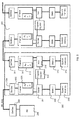
- a system for processing data flows may comprise a data flow processing module 300 arranged for receiving, transmitting, processing, storing and retrieving communications data.
- communications data may be received from and transmitted to the RE 206 of FIG.2 and the module 300 may be incorporated in the REC 207 of FIG.2 .
- the module 300 may be "daisy-chained" with one or more like modules of FIG. 2 . (One further module 301 is shown in FIG.3 as an example).
- the data flow processing module 300 may include a first framer (framer1) 302 which may be operably coupled to the RE 206 though serialiser/desreialiser interfaces.303 and 304 included in the RE 206 and first framer 302 respectively.
- the first framer may also include an auxiliary interface 305.
- the module 300 may also include a first Direct Memory Access module (DMA1) 306 and a divider module 307.
- the divider module 307 may be operably coupled between the first framer 302 and, the first Direct Memory Access module (DMA 1) 306.
- the module 300 may further include a programming register 308 which may be operably coupled to the divider module 307.
- the DMA1 306 may also be operably coupled to a system memory module 309.
- the system memory module 309 may be included in the data flow processing module 300 or, in an alternative embodiment, may be external to the module 300.
- the framer 1 and the DMA1 and the divider module 306 may comprise a "CPRI lane.”
- a CPRI lane handles the reception and transmission of CPRI data included in the communications traffic (comprising IQ samples and control and management signals) which is received from and transmitted to the RE 207.
- the data flow processing module 300 may also include a second framer (framer2) 310 which may be operably coupled to a first framer in the daisy-chained module 301 through a serialiser/desreialiser interface 311 included in the second framer 310.
- the second framer 310 may also include an auxiliary interface 312 which may be operably coupled to the auxiliary interface 305 of the first framer 302.
- the module 300 may also include a second Direct Memory Access module (DMA2) 313 and a multiplexer module 314.
- the multiplexer module 314 may be operably coupled between the second framer 310 and, the second Direct Memory Access module (DMA 2) 313.
- the programming register 308 may be operably coupled to the multiplexer module 314.
- the DMA2 313 may also be operably coupled to a further system memory module 315.
- This further system memory module 315 may also be included in the data flow processing module 300 or, in an alternative embodiment, may be external to the module 300.
- the framer2 310 and the DMA2 313 and the multiplexer module 314 may comprise a second CPRI lane.
- the divider module 307 of the first CPRI lane may be operably coupled to the multiplexer module 314 of the second CPRI lane.
- a dataflow having a frame structure may be sent from the RE 206 to the first framer1 302 via the serialiser/deserialiser interfaces 303 and 304 respectively.
- the data flow in this example may comprise IQ data of one or more antenna carriers (AxC).
- the frame structure of the data flow may, for example, be configured in accordance with the CPRI Specification V4.1.
- the antenna carriers may have the same sampling rate (AxC1) or have one of two sampling rates, AxC1 or AxC2.
- the framer1 302 may transfer the entire received data flow to the second framer2 310 via their respective auxiliary interfaces 305, 312.
- the framer2 310 may further transfer the entire received dataflow to a first framer of the module 301 if a daisy-chained topology is desired.
- a similar data flow having a frame structure may be sent from the first framer1 302 of the module 300 to the RE 206 via their respective serialiser/deserialiser interfaces 304, 303.
- the dataflow may similarly comprise IQ data of one or more antenna carriers of the same sampling rate or of one of two sampling rates.
- the framer1 302 may also transmit to the RE 303, IQ data which it receives from the associated dataflow processing module 301 in the daisy-chained configuration via the framer2 310.
- a framer such as either of the framers 302, 310 of the dataflow processing module 300 of FIG. 3 , may comprise two parts; namely, a receive part and a transmit part.
- the receive part acts to extract IQ data from the received frames (from the RE 206) which are subsequently written into system memory by way of direct memory access (DMA).
- the transmit part constructs the appropriate CPRI frame structure. IQ data read via DMA from system memory along with control data are multiplexer together by this transmit part for transmission to the RE 206.
- each DMA module 306, 313 of FIG.3 may temporarily store received IQ data before transferring the data either to system memory (in a receive mode) or to a framer (in a transmit mode).
- Each DMA module 306, 313 may, likewise, contain a receive part and a transmit part.
- the receive part may be arranged to transfer the IQ data received by its associated framer from the framer to system memory via a write bus.
- a transmit part may be arranged to transfer IQ data from system memory to its associated framer via a read bus
- the data flow may comprise IQ data of antenna carriers all having the same sampling rate AxC1.
- the program register 308 may set an output, which is coupled to both the divider 307 and the multiplexer 314, which serves to put both the divider 307 and the multiplexer 314 in a bypass mode.
- each CPRI lane may be independent, in which case, he framer1 302 is connected through the divider 307 to the first DMA1 306 and the framer2 310 is connected through the multiplexer to the second DMA2 313.
- the data flow may comprise IQ data of antenna carriers all having the same sampling rate AxC1 and the divider 307 and the multiplexer 314 may again be set in a bypass mode by the program register 308.
- the first and second framers 302, 310 may be connected together through their auxiliary interfaces 305, 312.
- the first framer1 302 may be connected through the divider 307 to the first DMA1 306.
- the second framer2 310 may be active but the second DMA2 313 unit is not used.
- the data coming from the RE 206 or another REC may be received by the first framer1 302 and part of the data (one or some of the AxCs) may be transferred by the divider 307 to the first DMA1 306.
- This DMA module 306 may write the received data to the system memory 309. Additionally, all the received data may be passed by the first framer1 302 to the second framer2 310 via their respective auxiliary interfaces 305, 312.
- the second framer2 310 may transmit this data to another device.
- the first DMA1 306 may read data from the system memory 309 which the divider 307 sends directly to the first framer1 302.
- the first framer1 302 may then aggregate and transmit this data with data coming from another device received by the second framer2 310 and passed to the first framer1 302 through the auxiliary interfaces 305, 312.
- the data flow may comprise IQ data of antenna carriers having two different sampling rates AxC1, AxC2.
- the program register 308 may set an output, which is coupled to both the divider 307 and the multiplexer 314, which serves to switch both the divider 307 and the multiplexer 314 out of a bypass mode and into a dual sampling rate mode.
- the first and second framers 302, 310 may be operably coupled via their respective auxiliary interfaces 305, 312.
- the first framer1 302 may be selectively coupled to either the first DMA1 306 or to the second DMA2 313 depending on the settings of the divider 307 and multiplexer 314 and under the control of the program register 308. Both the second framer2 310 and the second DMA2 313 may be active in this third example of operation but they do not need to be operably coupled to one another.
- the data coming from the RE 206 or another REC is received by the first framer1 302 and the data of AxC's having a first sample rate AxC1 may be switched by the divider through to the first DMA1 306 which may write the data to the system memory 309.
- the data of AxC(s) having a different sampling rate AxC2 may be diverted by the divider 307 to the second DMA2 313 through the multiplexer 314.
- the DMA2 313 then may write the data to the second system memory 315. All the received data may be passed by the first framer1 302 to the second framer2 310 through their respective auxiliary interfaces 305, 312.
- the second framer2 310 may then transmit this data to another device, for example, another data flow processing module such as module 301 of FIG.3 ..
- the first DMA1 306 may read data of AxC(s) of a first sampling rate AxC1 from the first system memory 309 and the divider 307 may be arranged to transfer it to the first framer1 302.
- the second DMA2 313 may read data of a different sampling rate AxC2 from the second system memory 315.
- the multiplexer 314 may then transfer this data to the divider which, in turn transfers it to the first framer1 302.
- the first framer1 302 may then aggregate and transmit the data of both sampling rates AxC1, AxC2 along with data coming from another device (according to its mask) which is received by the second framer2 310 and passed to the first framer1 302 via the auxiliary interfaces 305,312.
- the divider 307 is responsible for separating data flows of different sampling rates and for sending or retrieving them to or from either the first or the second of the DMA modules 306, 313.
- the Multiplexer 314 enables connection of the second DMA2 313 to the first framer1 302 (via the divider 307). In a bypass mode the multiplexer 313 may transfer data from the second DMA2 313 to the second framer2 310 and vice versa .
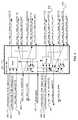
- FIG.4 is a simplified block diagram showing examples of logical elements which may comprise the divider 307 of FIG. 3 .
- a "mode select" signal on line 401 from the program register 308 may set the divider 307 in either a bypass mode, for cases where all IQ data has the same sampling rate, or a dual sampling rate mode, for cases where two sampling rates are present.
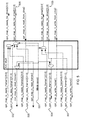
- FIG.5 is a simplified block diagram showing examples of logical elements which may comprise the multiplexer 314 of FIG. 3 .
- a "mode select" signal on line 501 from the program register 308 may set the multiplexer 314 in either a bypass mode, for cases where all IQ data has the same sampling rate, or a dual sampling rate mode, for cases where two sampling rates are present.
- dual sampling rate mode data received by the framer 1 302 and destined for the DMA2 315 may be input on line 502 from the divider 307.
- Data retrieved by the DMA2 313 on line 503 may be directed to the framer1 302 on line 504 (via the divider).
- bypass mode the multiplexer may transfer data between the second framer2 310 and the DMA2 313 via lines 505 and 506 for receive data and via lines 503 and 507 for transmit data.
- the divider module 307 and the multiplexer module 314 may be combined into a single module and one such single module may be incorporated in each CPRI lane of FIG.3 .
- the multiplexer of the single module included in the first lane and the divider of the single module included in the second lane will both be redundant and can be operated in bypass mode.
- FIG. 6 is a simplified flowchart illustrating an exemplary method 600 of processing data flows.
- a data flow which has a frame structure and includes IQ data of a first antenna carrier having a first sampling rate and IQ data of a second antenna carrier having a second sampling rate may be received at a framer, from a RE, for example.
- IQ data having only the first sampling rate may be diverted to a first Direct Memory Access module and IQ data having only the second sampling rate may be diverted to a second Direct Memory Access module.
- the data having only the first sampling rate may be transferred into a first memory and the data having only the second sampling rate may be transferred to a second memory.
- IQ data of a first antenna carrier having a first sampling rate may be transferred from a first Direct Memory Access module to the framer and IQ data of a second antenna carrier having a second sampling rate may be transferred from a second Direct Memory Access module to the framer.
- a frame structure including the first transmit data and the second transmit data is built by the framer for onward transmission, for example, to a RE.
- the invention may also be implemented in a computer program product for running on a computer system, at least including code portions for performing steps of a method according to the invention when run on a programmable apparatus, such as a computer system or enabling a programmable apparatus to perform functions of a device or system according to the invention.
- a tangible computer program product having executable code stored therein to perform a method for processing data flows, the method comprising; receiving, at a first framer, a receive data flow which has a frame structure and includes IQ data of a first antenna carrier having a first sampling rate and IQ data of a second antenna carrier having a second sampling rate, diverting IQ data having only the first sampling rate to a first Direct Memory Access module, diverting IQ data having only the second sampling rate to a second Direct Memory Access module, transferring first transmit IQ data of a first antenna carrier having a first sampling rate from a first Direct Memory Access module to a first framer, transferring second transmit IQ data of a second antenna carrier having a second sampling rate from a second Direct Memory Access module 313 to the first framer and building a frame structure including the first transmit IQ data and the second transmit IQ data for onward transmission.
- a computer program is a list of instructions such as a particular application program and/or an operating system.
- the computer program may for instance include one or more of: a subroutine, a function, a procedure, an object method, an object implementation, an executable application, an applet, a servlet, a source code, an object code, a shared library/dynamic load library and/or other sequence of instructions designed for execution on a computer system.
- a computer process typically includes an executing (running) program or portion of a program, current program values and state information, and the resources used by the operating system to manage the execution of the process.
- An operating system is the software that manages the sharing of the resources of a computer and provides programmers with an interface used to access those resources.
- An operating system processes system data and user input, and responds by allocating and managing tasks and internal system resources as a service to users and programs of the system.
- the computer system may for instance include at least one processing unit, associated memory and a number of input/output (I/O) devices.
- I/O input/output
- the computer system processes information according to the computer program and produces resultant output information via I/O devices.
- the invention has been described with reference to specific examples of embodiments of the invention. It will, however, be evident that various modifications and changes may be made therein without departing from the broader spirit and scope of the invention as set forth in the appended claims.
- the invention may be extended to process data flows of more than two different sampling rates. This may be achieved by employing additional DMA modules (one per sampling rate) and making the necessary modifications to the divide and multiplexer modules.
- connections as discussed herein may be any type of connection suitable to transfer signals from or to the respective nodes, units or devices, for example via intermediate devices. Accordingly, unless implied or stated otherwise, the connections may for example be direct connections or indirect connections.
- the connections may be illustrated or described in reference to being a single connection, a plurality of connections, unidirectional connections, or bidirectional connections. However, different embodiments may vary the implementation of the connections. For example, separate unidirectional connections may be used rather than bidirectional connections and vice versa.
- plurality of connections may be replaced with a single connections that transfers multiple signals serially or in a time multiplexed manner. Likewise, single connections carrying multiple signals may be separated out into various different connections carrying subsets of these signals. Therefore, many options exist for transferring signals.
- Each signal described herein may be designed as positive or negative logic.
- the signal In the case of a negative logic signal, the signal is active low where the logically true state corresponds to a logic level zero.
- the signal In the case of a positive logic signal, the signal is active high where the logically true state corresponds to a logic level one.
- any of the signals described herein can be designed as either negative or positive logic signals. Therefore, in alternate embodiments, those signals described as positive logic signals may be implemented as negative logic signals, and those signals described as negative logic signals may be implemented as positive logic signals.
- assert or “set” and “negate” (or “deassert” or “clear”) are used herein when referring to the rendering of a signal, status bit, or similar apparatus into its logically true or logically false state, respectively. If the logically true state is a logic level one, the logically false state is a logic level zero. And if the logically true state is a logic level zero, the logically false state is a logic level one.
- logic blocks are merely illustrative and that alternative embodiments may merge logic blocks or circuit elements or impose an alternate decomposition of functionality upon various logic blocks or circuit elements.
- architectures depicted herein are merely exemplary, and that in fact many other architectures can be implemented which achieve the same functionality.
- various alternative logic gate arrangements known to those skilled in the art may be configured in order to perform the same functionality as the divider and multiplexer modules illustrated in the drawings Any arrangement of components to achieve the same functionality is effectively "associated" such that the desired functionality is achieved.
- any two components herein combined to achieve a particular functionality can be seen as “associated with” each other such that the desired functionality is achieved, irrespective of architectures or intermedial components.
- any two components so associated can also be viewed as being “operably connected,” or “operably coupled,” to each other to achieve the desired functionality.
- an integrated circuit device may comprise one or more dies in a single package with electronic components provided on the dies that form the modules and which are connectable to other components outside the package through suitable connections, such as pins of the package and bondwires between the pins and the dies
- the examples, or portions thereof may implemented as soft or code representations of physical circuitry or of logical representations convertible into physical circuitry, such as in a hardware description language of any appropriate type.
- the invention is not limited to physical devices or units implemented in non-programmable hardware but can also be applied in programmable devices or units able to perform the desired device functions by operating in accordance with suitable program code, such as mainframes, minicomputers, servers, workstations, personal computers, notepads, personal digital assistants, electronic games, automotive and other embedded systems, cell phones and various other wireless devices, commonly denoted in this application as 'computer systems'.
- suitable program code such as mainframes, minicomputers, servers, workstations, personal computers, notepads, personal digital assistants, electronic games, automotive and other embedded systems, cell phones and various other wireless devices, commonly denoted in this application as 'computer systems'.
- any reference signs placed between parentheses shall not be construed as limiting the claim.
- the word 'comprising' does not exclude the presence of other elements or steps then those listed in a claim.
- the terms "a” or "an,” as used herein, are defined as one or more than one.
Landscapes
- Engineering & Computer Science (AREA)
- Computer Networks & Wireless Communication (AREA)
- Signal Processing (AREA)
- Mobile Radio Communication Systems (AREA)
Abstract
Description
- This invention relates to a system and method for processing data flows and particularly, though not exclusively, to such a system and method for processing flow of data in cellular communications networks.
- In a typical cellular communications system, wireless user equipment units (UEs), for example, mobile phones, communicate via a radio access network to one or more core networks. A radio access network covers a geographical area which is divided into cells, with each cell area being served by a radio base station. Several base stations are connected, typically via land lines, to a control node known as a radio network controller (RNC). Such a control node supervises and coordinates various activities of the several radio base stations which are connected to it. The radio network controllers are typically connected to one or more core networks. One example of a radio access network is the Universal Mobile Telecommunications (UMTS) Terrestrial Radio Access Network (UTRAN). The UMTS is a third generation (3G) system and UTRAN is essentially a radio access network providing wideband code division multiple access (WCDMA) to user equipment units. Fourth generation systems are evolving towards a broadband and mobile system. The 3rd Generation Partnership Project has proposed a Long Term Evolution (LTE) solution, namely, an Evolved Universal Mobile Telecommunication System Territorial Radio Access Network, (E-UTRAN), for a mobile access network.
- In many radio access networks the radio base station is a concentrated node with most of its components being located at a concentrated site. However, a radio base station can also be configured with a more distributed architecture. For example, a distributed radio base station can take the form of one or more radio equipment (RE) portions that are linked to a radio equipment control (REC) portion over an internal interface. One example of an internal interface of a radio base station which links a radio equipment portion of the radio base station to a radio equipment control portion of the base station is the Common Public Radio Interface (CPRI). The Common Public Radio Interface (CPRI) is described in Common Public Radio Interface (CPRI) Interface Specification Version 4.1 (18 February 2009) and also Version 4.2 (2010) and Version 5(2011).
- The Common Public Radio Interface (CPRI) is an industry cooperation aimed at defining a publicly available specification for the key internal interface of radio base stations between radio equipment control (REC) and radio equipment (RE), thereby allowing base station manufacturers to share a common protocol and more easily adapt platforms from one customer to another. In essence, a radio base station is decomposed into two separate blocks, known as REC and RE. The REC provides access to a UMTS network, for example, via the lub interface, whereas the RE serves as the air interface to user equipment, known as Uu in a UMTS network. The REC generally comprises the radio functions of the digital baseband domain, whereas the RE contains analogue radio frequency functions. The functional split between the REC and RE is done in such a way that a generic interface, CPRI, based on In-Phase and Quadrature (IQ) data can be defined. Several IQ data flows can be sent over one physical link with each data flow reflecting the data of one antenna for one carrier, the so-called antenna carrier "AxC." Several AxC's having the same sampling rate may be aggregated into an "AxC Group." IQ data of different antennas along with control data are multiplexed onto a transmission line. The CPRI has a basic frame structure for carrying a control word and an IQ data block.
- The functional split between the REC and RE allows the RE to be positioned close to an associated antenna. This reduces the distance which the associated signals have to travel before they are received by the RE, thereby negating the need for tower-mounted amplifiers and antenna system controllers. The link between the RE and REC is generally optical, allowing the link length to be much greater when compared with wired coaxial systems. Therefore, the distance between the RE and RRC can be around10Km, thereby increasing the flexibility of deployment of RE's within the network when utilising CPRI. One REC may be linked to two or more RE's or one RE may be linked to multiple REC's in a chain topology with each REC being configured to forward data to other REC's in the chain.
- Many of the functions which an REC has to perform, which include channel coding/encoding, spreading/despeading, frame and time slot generation, for example, may be realised by a proprietary digital signal processing device. Two examples of such DSP devices which support the CPRI are the Freescale B4860 and the Freescale MSC 8157 Broadband Wireless, Access Six Core DSP which is described in Freescale Semiconductor Data Sheet MSC8157E, 11/2011. This Digital Signal Processor includes (inter alia) a CPRI unit which includes a "framer" module which handles the transmission and reception of all IQ data, and a DMA (direct memory access) module associated with the framer which transfers the receive and transmit IQ data to and from antenna carrier buffers in a memory.
- Usually, the sampling rates of all AxC's in a CPRI unit are the same. A single CPRI unit will normally support only one AxC sample rate. If different sampling rates need to be supported, however, additional circuitry is required. One known way of supporting two sampling rates in the MSC8157 device employs three CPRI units.
FIG. 1 shows an example of this known solution. In the receive direction, afirst framer 101 receives RF data (from anRE 102 for example) and its associatedDMA module 103 transfers data with a first sampling rate tosystem memory 104. Asecond framer 105 receives the RF data from thefirst framer 101 viaauxiliary interface modules links third framer 110. ADMA module 111 associated with thethird framer 110 transfers data with a second sampling rate tosystem memory 112. In the transmit direction, theDMA module 103 associated with thefirst framer 101 fetches data with the first sampling rate fromsystem memory 104 and transfers it to thefirst framer 101 for outputting towards theRE 102. The third framer'sDMA module 111 fetches data with the second sampling rate fromsystem memory 112 and thethird framer 110 transfers the data to thesecond framer 105 via the serialiser/deserialiser second framer 105 transfers the data with the second sampling rate via theauxiliary interfaces first framer 101 which, in turn, outputs the data towards theRE 102. Each CPRI unit contains receive and transmit configuration tables that determine which AxC's in a frame to transfer to or fetch from system memory and their location in the frame. Further, each CPRI unit contains receive mask registers (not shown) with the masking of bits of theauxiliary interface framer2 105 is sent to theRE 102. Conversely, if the masking bit is "cleared" then the data read byframer1 101 fromsystem memory 104 is sent to theRE 102. This solution has the disadvantage of requiring an extra CPRI unit and interconnections. - The present invention provides a system and method for processing data flows as described in the accompanying claims.
- Specific embodiments of the invention are set forth in the dependent claims.
- These and other aspects of the invention will be apparent from and elucidated with reference to the embodiments described hereinafter.
- Further details, aspects and embodiments of the invention will be described, by way of example only, with reference to the drawings. In the drawings, like reference numbers are used to identify like or functionally similar elements. Elements in the figures are illustrated for simplicity and clarity and have not necessarily been drawn to scale.
-
FIG. 1 is a simplified block diagram of an example of a known system for processing data flows; -
FIG. 2 is a simplified schematic diagram of a wireless communication system including an example of a system for processing data flows; -
FIG.3 is a simplified block diagram of an example of a system for processing data flows; -
FIG.4 is a simplified block diagram of an example of a divider module; -
FIG. 5 is a simplified block diagram of an example of a multiplexer module; and -
FIG. 6 is a simplified flowchart illustrating an exemplary method of processing data flows. - Because the illustrated embodiments of the present invention may for the most part, be implemented using electronic components and circuits known to those skilled in the art, details will not be explained in any greater extent than that considered necessary as illustrated above, for the understanding and appreciation of the underlying concepts of the present invention and in order not to obfuscate or distract from the teachings of the present invention.
- Referring now to
FIG.2 , an example of part of a wireless communication system operating in accordance with embodiments of the invention is illustrated and indicated generally at 200 and comprises a 3G macro cell whose coverage area is indicated at 201. - A
core network 202 of the wireless communication system ofFIG.2 , which includes a Mobile Switching Centre (MSC) and other network elements (not shown), may serve to interface thewireless communication system 200 with a packet data network, for example a Public Switched Data Network (PSDN), (such as the internet) or a Public Switched Telephone Network (PSTN). - The
3G macro-cell 201 may be served by a radio base station (or "Node B") 203 which may be controlled by a Radio Network Controller (RNC) 204. TheRNC 204 may be linked to thecore network 202. - Typically, the
node B 203 may be arranged to receive signals coming from amobile device 205 located in themacrocell 101 and down-convert them to digital data. Encoded signals are then brought back to baseband before being transmitted to the terrestrial network (that is the core network 202). Similarly, thenode B 203 may be arranged to receive signals from thecore network 202 and convert these for transmission over a wireless interface to amobile unit 205 in themacrocell 201. - In this example, the
node B 203 is a distributed radio base station and comprises a radio equipment portion (RE) 206 and a radio equipment control portion (REC) 207. TheREC 207 may be linked to theRNC 204 over the so-called "lub" interface. TheRE 206 may be coupled to anantenna 208 which may communicate wirelessly with amobile unit 205 located within the macrocell's area ofcoverage 201 over the so-called "Uu" interface. - In such a distributed node B, information transfer between the radio equipment control (REC)
portion 207 and the radio equipment (RE)portion 206 may occur by use of a parallel control word transmitted over an internal interface, for example the co-called Common Public Radio Interface ( CPRI). Data communication by theREC 207 with the core network side of thenode B 203, as well as data communication byRE 206 with the antenna side of thenode B 203, occurs by serial communication. - The
REC 207 andRE 206 may be physically separated. For example, theRE 206 may be close to theantenna 208 and theREC 207 may be located in a conveniently accessible site. Alternatively, bothREC 207 andRE 206 may be co-located. - In this example, the
REC 207 may provide access to thecore network 203 via the lub interface and so may be primarily concerned with lub transport and lub protocols, control and management of the node B and digital baseband processing. For the downlink (that is theREC 207 to RE 206), theREC 207 may be arranged to handle such operations as channel coding, interleaving, spreading, scrambling, adding of physical channels, controlling transmit power of each physical channel, frame and slot signal generation (including clock stabilization). For the uplink (that is fromRE 206 to REC 207), theREC 207 handles such operations as channel de-coding, deinterleaving, de-spreading, de-scrambling, signal distribution to signal processing units, detection of feedback information for transmit power control, and signal to interference ratio measurement. - The
radio equipment RE 206 may be arranged to serve the air interface Uu to themobile unit 205 by providing the analogue and radio frequency functions such as filtering, modulation, frequency conversion and amplification. For the downlink,RE 206 may perform operations such as digital to analogue conversion, up conversion, on/off control of each carrier, carrier multiplexing, power amplification and limiting, antenna supervision, and RF filtering. For the uplink, the RE may perform operations such as analogue to digital conversion, down conversion, automatic gain control, carrier de-multiplexing, low noise amplification, and RF filtering. Thus, theREC 207 comprises the radio functions of the digital baseband domain, whereas theRE 206 comprises the analogue radio frequency functions. The functional split between both parts is done in such a way that a generic interface based on In-Phase and Quadrature (IQ) data can be defined. - The Common Public Radio Interface (CPRI) Interface Specification (See Version 4.1 for example) defines protocols for a physical layer (layer 1) and a data link layer (layer 2).
Layer 1 defines, e.g., electrical characteristics, optical characteristics, time division multiplexing of the different data flows, and low level signaling.Layer 2 defines the media access control, flow control and data protection of the control and management information flow. Information flow over the parallel communications links 26 ofnode B 203 is carried in frames. In the example implementation which is compatible with Common Public Radio Interface Specification Version - Referring now to
FIG. 3 a system for processing data flows may comprise a dataflow processing module 300 arranged for receiving, transmitting, processing, storing and retrieving communications data. - In this example, communications data may be received from and transmitted to the
RE 206 ofFIG.2 and themodule 300 may be incorporated in theREC 207 ofFIG.2 . Themodule 300 may be "daisy-chained" with one or more like modules ofFIG. 2 . (Onefurther module 301 is shown inFIG.3 as an example). - The data
flow processing module 300 may include a first framer (framer1) 302 which may be operably coupled to theRE 206 though serialiser/desreialiser interfaces.303 and 304 included in theRE 206 andfirst framer 302 respectively. The first framer may also include anauxiliary interface 305. Themodule 300 may also include a first Direct Memory Access module (DMA1) 306 and adivider module 307. Thedivider module 307 may be operably coupled between thefirst framer 302 and, the first Direct Memory Access module (DMA 1) 306. Themodule 300 may further include aprogramming register 308 which may be operably coupled to thedivider module 307. TheDMA1 306 may also be operably coupled to asystem memory module 309. Thesystem memory module 309 may be included in the dataflow processing module 300 or, in an alternative embodiment, may be external to themodule 300. - The
framer 1 and the DMA1 and thedivider module 306 may comprise a "CPRI lane." A CPRI lane handles the reception and transmission of CPRI data included in the communications traffic (comprising IQ samples and control and management signals) which is received from and transmitted to theRE 207. - The data
flow processing module 300 may also include a second framer (framer2) 310 which may be operably coupled to a first framer in the daisy-chainedmodule 301 through a serialiser/desreialiser interface 311 included in thesecond framer 310. Thesecond framer 310 may also include anauxiliary interface 312 which may be operably coupled to theauxiliary interface 305 of thefirst framer 302. Themodule 300 may also include a second Direct Memory Access module (DMA2) 313 and amultiplexer module 314. Themultiplexer module 314 may be operably coupled between thesecond framer 310 and, the second Direct Memory Access module (DMA 2) 313. Theprogramming register 308 may be operably coupled to themultiplexer module 314. TheDMA2 313 may also be operably coupled to a furthersystem memory module 315. This furthersystem memory module 315 may also be included in the dataflow processing module 300 or, in an alternative embodiment, may be external to themodule 300. Theframer2 310 and theDMA2 313 and themultiplexer module 314 may comprise a second CPRI lane. Thedivider module 307 of the first CPRI lane may be operably coupled to themultiplexer module 314 of the second CPRI lane. - In one example embodiment, in a receive mode (uplink) of operation a dataflow having a frame structure may be sent from the
RE 206 to thefirst framer1 302 via the serialiser/deserialiser interfaces framer1 302 may transfer the entire received data flow to thesecond framer2 310 via their respectiveauxiliary interfaces framer2 310 may further transfer the entire received dataflow to a first framer of themodule 301 if a daisy-chained topology is desired. - In a transmit mode (downlink), a similar data flow having a frame structure may be sent from the
first framer1 302 of themodule 300 to theRE 206 via their respective serialiser/deserialiser interfaces framer1 302 may also transmit to theRE 303, IQ data which it receives from the associateddataflow processing module 301 in the daisy-chained configuration via theframer2 310. - In general, a framer such as either of the
framers dataflow processing module 300 ofFIG. 3 , may comprise two parts; namely, a receive part and a transmit part. The receive part acts to extract IQ data from the received frames (from the RE 206) which are subsequently written into system memory by way of direct memory access (DMA). The transmit part constructs the appropriate CPRI frame structure. IQ data read via DMA from system memory along with control data are multiplexer together by this transmit part for transmission to theRE 206. - Thus, each
DMA module FIG.3 may temporarily store received IQ data before transferring the data either to system memory (in a receive mode) or to a framer (in a transmit mode). EachDMA module - In a first exemplary mode of operation the data flow may comprise IQ data of antenna carriers all having the same sampling rate AxC1. The
program register 308 may set an output, which is coupled to both thedivider 307 and themultiplexer 314, which serves to put both thedivider 307 and themultiplexer 314 in a bypass mode. In this first exemplary mode, each CPRI lane may be independent, in which case, he framer1 302 is connected through thedivider 307 to thefirst DMA1 306 and theframer2 310 is connected through the multiplexer to thesecond DMA2 313. In the receive path thedivider 307 acts to directly transfer the entire data received byframer1 302 to DMA1 306.and themultiplexer 314 acts to directly transfer the entire data received by framer2 toDMA2 313. The data received by either framer 302,310 may originate from theRE 206 or from another REC. Each DMA module 306,313 may write the data to its respective system memory. 309,315. In the transmit path, thedivider 307 acts to directly transfer data whichDMA1 306 may read fromsystem memory 309 to thefirst framer1 302. Also, themultiplexer 314 acts to directly transfer data whichDMA2 313 may read fromsystem memory 315 to thesecond framer2 310. Eachframer RE 206 or another REC. - In a second exemplary mode of operation, the data flow may comprise IQ data of antenna carriers all having the same sampling rate AxC1 and the
divider 307 and themultiplexer 314 may again be set in a bypass mode by theprogram register 308. Also in this mode, the first andsecond framers auxiliary interfaces first framer1 302 may be connected through thedivider 307 to thefirst DMA1 306. Thesecond framer2 310 may be active but thesecond DMA2 313 unit is not used. In the receive path the data coming from theRE 206 or another REC may be received by thefirst framer1 302 and part of the data (one or some of the AxCs) may be transferred by thedivider 307 to thefirst DMA1 306. ThisDMA module 306 may write the received data to thesystem memory 309. Additionally, all the received data may be passed by thefirst framer1 302 to thesecond framer2 310 via their respectiveauxiliary interfaces second framer2 310 may transmit this data to another device. In the transmit path thefirst DMA1 306 may read data from thesystem memory 309 which thedivider 307 sends directly to thefirst framer1 302. Thefirst framer1 302 may then aggregate and transmit this data with data coming from another device received by thesecond framer2 310 and passed to thefirst framer1 302 through theauxiliary interfaces - In a third exemplary mode of operation, the data flow may comprise IQ data of antenna carriers having two different sampling rates AxC1, AxC2. The
program register 308 may set an output, which is coupled to both thedivider 307 and themultiplexer 314, which serves to switch both thedivider 307 and themultiplexer 314 out of a bypass mode and into a dual sampling rate mode. The first andsecond framers auxiliary interfaces first framer1 302 may be selectively coupled to either thefirst DMA1 306 or to thesecond DMA2 313 depending on the settings of thedivider 307 andmultiplexer 314 and under the control of theprogram register 308. Both thesecond framer2 310 and thesecond DMA2 313 may be active in this third example of operation but they do not need to be operably coupled to one another. - In the receive path the data coming from the
RE 206 or another REC is received by thefirst framer1 302 and the data of AxC's having a first sample rate AxC1 may be switched by the divider through to thefirst DMA1 306 which may write the data to thesystem memory 309. The data of AxC(s) having a different sampling rate AxC2 may be diverted by thedivider 307 to thesecond DMA2 313 through themultiplexer 314. TheDMA2 313 then may write the data to thesecond system memory 315. All the received data may be passed by thefirst framer1 302 to thesecond framer2 310 through their respectiveauxiliary interfaces second framer2 310 may then transmit this data to another device, for example, another data flow processing module such asmodule 301 ofFIG.3 .. - In the transmit path the
first DMA1 306 may read data of AxC(s) of a first sampling rate AxC1 from thefirst system memory 309 and thedivider 307 may be arranged to transfer it to thefirst framer1 302. Thesecond DMA2 313 may read data of a different sampling rate AxC2 from thesecond system memory 315. Themultiplexer 314 may then transfer this data to the divider which, in turn transfers it to thefirst framer1 302. Thefirst framer1 302 may then aggregate and transmit the data of both sampling rates AxC1, AxC2 along with data coming from another device (according to its mask) which is received by thesecond framer2 310 and passed to thefirst framer1 302 via the auxiliary interfaces 305,312. In this third example of operation, thedivider 307 is responsible for separating data flows of different sampling rates and for sending or retrieving them to or from either the first or the second of theDMA modules Multiplexer 314 enables connection of thesecond DMA2 313 to the first framer1 302 (via the divider 307). In a bypass mode themultiplexer 313 may transfer data from thesecond DMA2 313 to thesecond framer2 310 and vice versa. - Reference will now be made to
FIG.4 which is a simplified block diagram showing examples of logical elements which may comprise thedivider 307 ofFIG. 3 . A "mode select" signal online 401 from theprogram register 308 may set thedivider 307 in either a bypass mode, for cases where all IQ data has the same sampling rate, or a dual sampling rate mode, for cases where two sampling rates are present. Further control signals from theprogram register 308 on lines 402-405 and theframer1 307 onlines framer1 302 online 408 and to forward data retrieved from eitherDMA1 306 on line 409 or DMA2 315 (via the multiplexer 314) online 410 to theframer1 302. - Reference will now be made to
FIG.5 which is a simplified block diagram showing examples of logical elements which may comprise themultiplexer 314 ofFIG. 3 . A "mode select" signal online 501 from theprogram register 308 may set themultiplexer 314 in either a bypass mode, for cases where all IQ data has the same sampling rate, or a dual sampling rate mode, for cases where two sampling rates are present. In dual sampling rate mode, data received by theframer 1 302 and destined for theDMA2 315 may be input online 502 from thedivider 307. Data retrieved by theDMA2 313 online 503 may be directed to theframer1 302 on line 504 (via the divider). In bypass mode, the multiplexer may transfer data between thesecond framer2 310 and theDMA2 313 vialines lines - In an alternative exemplary embodiment, the
divider module 307 and themultiplexer module 314 may be combined into a single module and one such single module may be incorporated in each CPRI lane ofFIG.3 . In this alternative example, in the dual sampling rate mode, the multiplexer of the single module included in the first lane and the divider of the single module included in the second lane will both be redundant and can be operated in bypass mode. - An example of a method for processing data flows will now be described with reference to
FIG. 6 which is a simplified flowchart illustrating anexemplary method 600 of processing data flows. In an uplink direction, at 601. a data flow which has a frame structure and includes IQ data of a first antenna carrier having a first sampling rate and IQ data of a second antenna carrier having a second sampling rate may be received at a framer, from a RE, for example. At 602, IQ data having only the first sampling rate may be diverted to a first Direct Memory Access module and IQ data having only the second sampling rate may be diverted to a second Direct Memory Access module. At 603, the data having only the first sampling rate may be transferred into a first memory and the data having only the second sampling rate may be transferred to a second memory. In a downlink direction, at 604, IQ data of a first antenna carrier having a first sampling rate may be transferred from a first Direct Memory Access module to the framer and IQ data of a second antenna carrier having a second sampling rate may be transferred from a second Direct Memory Access module to the framer. At 605 a frame structure including the first transmit data and the second transmit data is built by the framer for onward transmission, for example, to a RE. - The invention may also be implemented in a computer program product for running on a computer system, at least including code portions for performing steps of a method according to the invention when run on a programmable apparatus, such as a computer system or enabling a programmable apparatus to perform functions of a device or system according to the invention. As an example, a tangible computer program product may be provided having executable code stored therein to perform a method for processing data flows, the method comprising; receiving, at a first framer, a receive data flow which has a frame structure and includes IQ data of a first antenna carrier having a first sampling rate and IQ data of a second antenna carrier having a second sampling rate, diverting IQ data having only the first sampling rate to a first Direct Memory Access module, diverting IQ data having only the second sampling rate to a second Direct Memory Access module, transferring first transmit IQ data of a first antenna carrier having a first sampling rate from a first Direct Memory Access module to a first framer, transferring second transmit IQ data of a second antenna carrier having a second sampling rate from a second Direct
Memory Access module 313 to the first framer and building a frame structure including the first transmit IQ data and the second transmit IQ data for onward transmission. - A computer program is a list of instructions such as a particular application program and/or an operating system. The computer program may for instance include one or more of: a subroutine, a function, a procedure, an object method, an object implementation, an executable application, an applet, a servlet, a source code, an object code, a shared library/dynamic load library and/or other sequence of instructions designed for execution on a computer system.
- The computer program may be stored internally on computer readable storage medium or transmitted to the computer system via a computer readable transmission medium. All or some of the computer program may be provided on tangible computer readable media permanently, removably or remotely coupled to an information processing system. The computer readable media may include, for example and without limitation, any number of the following: magnetic storage media including disk and tape storage media; optical storage media such as compact disk media (e.g., CD-ROM, CD-R, etc.) and digital video disk storage media; nonvolatile memory storage media including semiconductor-based memory units such as FLASH memory, EEPROM, EPROM, ROM; ferromagnetic digital memories; MRAM; volatile storage media including registers, buffers or caches, main memory, RAM, etc.
- A computer process typically includes an executing (running) program or portion of a program, current program values and state information, and the resources used by the operating system to manage the execution of the process. An operating system (OS) is the software that manages the sharing of the resources of a computer and provides programmers with an interface used to access those resources. An operating system processes system data and user input, and responds by allocating and managing tasks and internal system resources as a service to users and programs of the system.
- The computer system may for instance include at least one processing unit, associated memory and a number of input/output (I/O) devices. When executing the computer program, the computer system processes information according to the computer program and produces resultant output information via I/O devices.
- In the foregoing specification, the invention has been described with reference to specific examples of embodiments of the invention. It will, however, be evident that various modifications and changes may be made therein without departing from the broader spirit and scope of the invention as set forth in the appended claims. For example, the invention may be extended to process data flows of more than two different sampling rates. This may be achieved by employing additional DMA modules (one per sampling rate) and making the necessary modifications to the divide and multiplexer modules.
- The connections as discussed herein may be any type of connection suitable to transfer signals from or to the respective nodes, units or devices, for example via intermediate devices. Accordingly, unless implied or stated otherwise, the connections may for example be direct connections or indirect connections. The connections may be illustrated or described in reference to being a single connection, a plurality of connections, unidirectional connections, or bidirectional connections. However, different embodiments may vary the implementation of the connections. For example, separate unidirectional connections may be used rather than bidirectional connections and vice versa. Also, plurality of connections may be replaced with a single connections that transfers multiple signals serially or in a time multiplexed manner. Likewise, single connections carrying multiple signals may be separated out into various different connections carrying subsets of these signals. Therefore, many options exist for transferring signals.
- Each signal described herein may be designed as positive or negative logic. In the case of a negative logic signal, the signal is active low where the logically true state corresponds to a logic level zero. In the case of a positive logic signal, the signal is active high where the logically true state corresponds to a logic level one. Note that any of the signals described herein can be designed as either negative or positive logic signals. Therefore, in alternate embodiments, those signals described as positive logic signals may be implemented as negative logic signals, and those signals described as negative logic signals may be implemented as positive logic signals.
- Furthermore, the terms "assert" or "set" and "negate" (or "deassert" or "clear") are used herein when referring to the rendering of a signal, status bit, or similar apparatus into its logically true or logically false state, respectively. If the logically true state is a logic level one, the logically false state is a logic level zero. And if the logically true state is a logic level zero, the logically false state is a logic level one.
- Those skilled in the art will recognize that the boundaries between logic blocks are merely illustrative and that alternative embodiments may merge logic blocks or circuit elements or impose an alternate decomposition of functionality upon various logic blocks or circuit elements. Thus, it is to be understood that the architectures depicted herein are merely exemplary, and that in fact many other architectures can be implemented which achieve the same functionality. For example, various alternative logic gate arrangements known to those skilled in the art may be configured in order to perform the same functionality as the divider and multiplexer modules illustrated in the drawings Any arrangement of components to achieve the same functionality is effectively "associated" such that the desired functionality is achieved. Hence, any two components herein combined to achieve a particular functionality can be seen as "associated with" each other such that the desired functionality is achieved, irrespective of architectures or intermedial components. Likewise, any two components so associated can also be viewed as being "operably connected," or "operably coupled," to each other to achieve the desired functionality.
- Furthermore, those skilled in the art will recognize that boundaries between the above described operations merely illustrative. The multiple operations may be combined into a single operation, a single operation may be distributed in additional operations and operations may be executed at least partially overlapping in time. Moreover, alternative embodiments may include multiple instances of a particular operation, and the order of operations may be altered in various other embodiment.
- The illustrated examples of the
divider 307 andmultiplexer 314 may be implemented as any number of separate integrated circuits or separate devices interconnected with each other in a suitable manner. Furthermore themodule 300 may be implemented in one or several integrated circuits. - For example, an integrated circuit device may comprise one or more dies in a single package with electronic components provided on the dies that form the modules and which are connectable to other components outside the package through suitable connections, such as pins of the package and bondwires between the pins and the dies
- Also for example, the examples, or portions thereof, may implemented as soft or code representations of physical circuitry or of logical representations convertible into physical circuitry, such as in a hardware description language of any appropriate type.
- Also, the invention is not limited to physical devices or units implemented in non-programmable hardware but can also be applied in programmable devices or units able to perform the desired device functions by operating in accordance with suitable program code, such as mainframes, minicomputers, servers, workstations, personal computers, notepads, personal digital assistants, electronic games, automotive and other embedded systems, cell phones and various other wireless devices, commonly denoted in this application as 'computer systems'.
- However, other modifications, variations and alternatives are also possible. The specifications and drawings are, accordingly, to be regarded in an illustrative rather than in a restrictive sense.
- In the claims, any reference signs placed between parentheses shall not be construed as limiting the claim. The word 'comprising' does not exclude the presence of other elements or steps then those listed in a claim. Furthermore, the terms "a" or "an," as used herein, are defined as one or more than one. Also, the use of introductory phrases such as "at least one" and "one or more" in the claims should not be construed to imply that the introduction of another claim element by the indefinite articles "a" or "an" limits any particular claim containing such introduced claim element to inventions containing only one such element, even when the same claim includes the introductory phrases "one or more" or "at least one" and indefinite articles such as "a" or "an." The same holds true for the use of definite articles. Unless stated otherwise, terms such as "first" and "second" are used to arbitrarily distinguish between the elements such terms describe. Thus, these terms are not necessarily intended to indicate temporal or other prioritization of such elements The mere fact that certain measures are recited in mutually different claims does not indicate that a combination of these measures cannot be used to advantage.
Claims (9)
- A method of processing data flows comprising receiving (601) at a first framer (302) a receive data flow which includes IQ data of a first antenna carrier having a first sampling rate and IQ data of a second antenna carrier having a second sampling rate, diverting (602) IQ data having only the first sampling rate to a first Direct Memory Access module (306), diverting (602) IQ data having only the second sampling rate to a second Direct Memory Access module (313), transferring (604) first transmit IQ data of a first antenna carrier having a first sampling rate from a first Direct Memory Access module 313 to a first framer 302, transferring (604) second transmit IQ data of a second antenna carrier having a second sampling rate from a second Direct Memory Access module 313 to the first framer 302, building (605) a frame structure including the first transmit IQ data and the second transmit IQ data for onward transmission.
- The method of claim 1 including transferring (603) the data having only the first sampling rate to a first memory (309) and transferring (603) the data having only the second sampling rate to a second memory (315).
- The method of claim 1 or claim 2 including building (605) a frame structure including IQ data received from a second framer (310).
- A system (300) for processing data flows comprising a first framer (302) for receiving a data flow which includes IQ data of a first antenna carrier having a first sampling rate and IQ data of a second antenna carrier having a second sampling rate, the system further comprising a diverter arrangement (307, 314), a first Direct Memory Access module (306) and a second Direct Memory Access module (313) wherein the diverter arrangement (307, 314) is arranged to divert IQ data having only the first sampling rate to the first Direct Memory Access module (306) and to divert (602) IQ data having only the second sampling rate to a second Direct Memory Access module (313) and to transfer first transmit IQ data of a first antenna carrier having a first sampling rate from the first Direct Memory Access module (313) to the first framer (302) and to transfer second IQ data of a second antenna carrier having a second sampling rate from the second Direct Memory Access module (313) to the first framer (302), and wherein the first framer (302) is arranged to build a frame structure including the first transmit data and the second transmit data for onward transmission.
- The system of claim 4 wherein the first framer (302) is arranged to build a frame structure including IQ data received from a second framer (310).
- A system (300) for processing data flows comprising a first processing lane and a second processing lane, wherein the first processing lane comprises a first framer (302) arranged to receive a first receive data flow which includes IQ data of one or more antenna carriers each having a sampling rate associated therewith, a first diverter module (307) and a first Direct Memory Access module (306), and wherein the second processing lane comprises a second framer (310) arranged to receive a second receive data flow which includes IQ data of one or more antenna carriers each having a sampling rate associated therewith, a second diverter module (314) and a second Direct Memory Access module (313),wherein, in a first, single sampling rate mode of operation, the first diverter module (307) is arranged to selectively divert IQ data of the first receive data flow from the first framer (302) to the first Direct Memory Access module (306) and to transfer first transmit IQ data from the first Direct Memory Access module (306) to the first framer (302), and wherein the second diverter module (3314) is arranged to transfer IQ data of the second receive data flow from the second framer (310) to the second Direct Memory Access module (313) and to selectively divert second transmit IQ data from the second Direct Memory Access module (313) to the second framer (310), and wherein in a second, dual sampling rate mode of operation, the first diverter(307) is arranged to selectively divert IQ data of the first receive data flow having a first sampling rate to the first Direct Memory Access module (306) and to selectively divert IQ data of the first receive data flow having a second sampling rate to the second diverter module (314) and to transfer first transmit IQ data of a first antenna carrier having a first sampling rate from the first Direct Memory Access module (313) to the first framer (302) and to transfer second transmit IQ data of a second carrier having a second sampling rate from the second diverter module (314) to the first framer (302), and wherein the second diverter module (314) is arranged to transfer IQ data of the first receive data flow having a second sampling rate from the first diverter (307) to the second Direct Memory Access module (313) and to selectively divert second transmit IQ data of a second antenna carrier having a second sampling rate from the second Direct Memory Access module (313) to the first diverter module (307), and wherein the first framer (302) is arranged to build a frame structure including the first transmit IQ data and the second transmit IQ data for onward transmission.
- The system of claim 6 wherein the second framer (310) is arranged to receive a receive data flow from the first framer (302) and to forward it to a remote device and to receive remote transmit IQ data from a remote device and forward it to the first framer (302) and wherein the first framer (302) is arranged to build a frame structure including the remote transmit IQ data for onward transmission.
- The system of any of claims 4 to 7 wherein the system is implemented in one or more integrated circuit devices.
- A computer program product having executable code stored therein to perform a method for processing data flows in accordance with claim 1.
Priority Applications (1)
| Application Number | Priority Date | Filing Date | Title |
|---|---|---|---|
| EP13150356.7A EP2753039B1 (en) | 2013-01-07 | 2013-01-07 | System and method for processing data flows |
Applications Claiming Priority (1)
| Application Number | Priority Date | Filing Date | Title |
|---|---|---|---|
| EP13150356.7A EP2753039B1 (en) | 2013-01-07 | 2013-01-07 | System and method for processing data flows |
Publications (2)
| Publication Number | Publication Date |
|---|---|
| EP2753039A1 true EP2753039A1 (en) | 2014-07-09 |
| EP2753039B1 EP2753039B1 (en) | 2018-08-29 |
Family
ID=47552881
Family Applications (1)
| Application Number | Title | Priority Date | Filing Date |
|---|---|---|---|
| EP13150356.7A Not-in-force EP2753039B1 (en) | 2013-01-07 | 2013-01-07 | System and method for processing data flows |
Country Status (1)
| Country | Link |
|---|---|
| EP (1) | EP2753039B1 (en) |
Cited By (2)
| Publication number | Priority date | Publication date | Assignee | Title |
|---|---|---|---|---|
| CN109412655A (en) * | 2018-11-29 | 2019-03-01 | 京信通信系统(中国)有限公司 | Distributing antenna system, its I/Q data adaptive device and method |
| CN112584434A (en) * | 2019-09-30 | 2021-03-30 | 深圳市中兴微电子技术有限公司 | Data transmission method and device |
Citations (2)
| Publication number | Priority date | Publication date | Assignee | Title |
|---|---|---|---|---|
| US5965819A (en) * | 1998-07-06 | 1999-10-12 | Csi Technology | Parallel processing in a vibration analyzer |
| WO2010083377A1 (en) * | 2009-01-17 | 2010-07-22 | Qualcomm Incorporated | Ofdm time basis matching with pre-fft cyclic shift |
-
2013
- 2013-01-07 EP EP13150356.7A patent/EP2753039B1/en not_active Not-in-force
Patent Citations (2)
| Publication number | Priority date | Publication date | Assignee | Title |
|---|---|---|---|---|
| US5965819A (en) * | 1998-07-06 | 1999-10-12 | Csi Technology | Parallel processing in a vibration analyzer |
| WO2010083377A1 (en) * | 2009-01-17 | 2010-07-22 | Qualcomm Incorporated | Ofdm time basis matching with pre-fft cyclic shift |
Non-Patent Citations (1)
| Title |
|---|
| FREESCALE SEMICONDUCTORS: "MSC8157 Reference Manual", 31 January 2012, FREESCALE SEMICONDUCTORS, www.freescale.com/support, XP002698473 * |
Cited By (3)
| Publication number | Priority date | Publication date | Assignee | Title |
|---|---|---|---|---|
| CN109412655A (en) * | 2018-11-29 | 2019-03-01 | 京信通信系统(中国)有限公司 | Distributing antenna system, its I/Q data adaptive device and method |
| CN109412655B (en) * | 2018-11-29 | 2024-03-26 | 京信网络系统股份有限公司 | Distributed antenna system, IQ data adapting device and method thereof |
| CN112584434A (en) * | 2019-09-30 | 2021-03-30 | 深圳市中兴微电子技术有限公司 | Data transmission method and device |
Also Published As
| Publication number | Publication date |
|---|---|
| EP2753039B1 (en) | 2018-08-29 |
Similar Documents
| Publication | Publication Date | Title |
|---|---|---|
| US9635710B2 (en) | Method and apparatus for processing data flows | |
| US7460513B2 (en) | Encapsulation of diverse protocols over internal interface of distributed radio base station | |
| US9838885B2 (en) | Wireless communication system and method and expansion unit of flat network architecture | |
| US8606255B2 (en) | Asynchronous communication over common public radio interface (CPRI) | |
| CN102130716B (en) | The implementation method of high-speed mobile communications and equipment | |
| US20050105552A1 (en) | Encapsulation of independent transmissions over internal interface of distributed radio base station | |
| CN110557690B (en) | Radio remote hub RHUB, indoor communication system and signal transmission method | |
| US10225196B2 (en) | Apparatus, system and method for controlling packet data flow | |
| WO1999009769A1 (en) | Methods and apparatus for improved base station transceivers | |
| US11323171B2 (en) | System and method for a mobile communication coverage area | |
| US20190320486A1 (en) | Virtualized Wireless Base Stations Network | |
| US20160174128A1 (en) | Digital Distributed Antenna System | |
| US9461869B2 (en) | System and method for processing data flows | |
| CN113691359A (en) | Method and apparatus for replicating data transfer | |
| CN116530159A (en) | Uplink transmission method, terminal equipment and network equipment | |
| DK2687062T3 (en) | BASE STATION | |
| EP2753039B1 (en) | System and method for processing data flows | |
| US9730215B2 (en) | Method and device for interfacing in a mobile communication system | |
| US12401604B2 (en) | Wireless mesh network | |
| US20220416735A1 (en) | Methods and devices for increased efficiency in linear power amplifier | |
| US20110134772A1 (en) | Methods of radio communication involving multiple radio channels, and radio signal repeater and mobile station apparatuses implementing same | |
| CN114640714A (en) | 4G and 5G co-station method, 5G base station and storage medium | |
| CN106375063B (en) | Data transmission method and equipment thereof | |
| US11652730B2 (en) | Selective processing of traffic flows based on latency requirements | |
| US20250330971A1 (en) | Wireless communication method, terminal device, and network device |
Legal Events
| Date | Code | Title | Description |
|---|---|---|---|
| 17P | Request for examination filed |
Effective date: 20130107 |
|
| AK | Designated contracting states |
Kind code of ref document: A1 Designated state(s): AL AT BE BG CH CY CZ DE DK EE ES FI FR GB GR HR HU IE IS IT LI LT LU LV MC MK MT NL NO PL PT RO RS SE SI SK SM TR |
|
| AX | Request for extension of the european patent |
Extension state: BA ME |
|
| PUAI | Public reference made under article 153(3) epc to a published international application that has entered the european phase |
Free format text: ORIGINAL CODE: 0009012 |
|
| R17P | Request for examination filed (corrected) |
Effective date: 20150109 |
|
| RBV | Designated contracting states (corrected) |
Designated state(s): AL AT BE BG CH CY CZ DE DK EE ES FI FR GB GR HR HU IE IS IT LI LT LU LV MC MK MT NL NO PL PT RO RS SE SI SK SM TR |
|
| RAP1 | Party data changed (applicant data changed or rights of an application transferred) |
Owner name: NXP USA, INC. |
|
| STAA | Information on the status of an ep patent application or granted ep patent |
Free format text: STATUS: EXAMINATION IS IN PROGRESS |
|
| 17Q | First examination report despatched |
Effective date: 20170720 |
|
| GRAP | Despatch of communication of intention to grant a patent |
Free format text: ORIGINAL CODE: EPIDOSNIGR1 |
|
| STAA | Information on the status of an ep patent application or granted ep patent |
Free format text: STATUS: GRANT OF PATENT IS INTENDED |
|
| INTG | Intention to grant announced |
Effective date: 20180326 |
|
| GRAS | Grant fee paid |
Free format text: ORIGINAL CODE: EPIDOSNIGR3 |
|
| GRAA | (expected) grant |
Free format text: ORIGINAL CODE: 0009210 |
|
| STAA | Information on the status of an ep patent application or granted ep patent |
Free format text: STATUS: THE PATENT HAS BEEN GRANTED |
|
| AK | Designated contracting states |
Kind code of ref document: B1 Designated state(s): AL AT BE BG CH CY CZ DE DK EE ES FI FR GB GR HR HU IE IS IT LI LT LU LV MC MK MT NL NO PL PT RO RS SE SI SK SM TR |
|
| REG | Reference to a national code |
Ref country code: GB Ref legal event code: FG4D |
|
| REG | Reference to a national code |
Ref country code: CH Ref legal event code: EP |
|
| REG | Reference to a national code |
Ref country code: AT Ref legal event code: REF Ref document number: 1036492 Country of ref document: AT Kind code of ref document: T Effective date: 20180915 |
|
| REG | Reference to a national code |
Ref country code: IE Ref legal event code: FG4D |
|
| REG | Reference to a national code |
Ref country code: DE Ref legal event code: R096 Ref document number: 602013042632 Country of ref document: DE |
|
| REG | Reference to a national code |
Ref country code: NL Ref legal event code: MP Effective date: 20180829 |
|
| REG | Reference to a national code |
Ref country code: LT Ref legal event code: MG4D |
|
| PG25 | Lapsed in a contracting state [announced via postgrant information from national office to epo] |
Ref country code: LT Free format text: LAPSE BECAUSE OF FAILURE TO SUBMIT A TRANSLATION OF THE DESCRIPTION OR TO PAY THE FEE WITHIN THE PRESCRIBED TIME-LIMIT Effective date: 20180829 Ref country code: GR Free format text: LAPSE BECAUSE OF FAILURE TO SUBMIT A TRANSLATION OF THE DESCRIPTION OR TO PAY THE FEE WITHIN THE PRESCRIBED TIME-LIMIT Effective date: 20181130 Ref country code: FI Free format text: LAPSE BECAUSE OF FAILURE TO SUBMIT A TRANSLATION OF THE DESCRIPTION OR TO PAY THE FEE WITHIN THE PRESCRIBED TIME-LIMIT Effective date: 20180829 Ref country code: NO Free format text: LAPSE BECAUSE OF FAILURE TO SUBMIT A TRANSLATION OF THE DESCRIPTION OR TO PAY THE FEE WITHIN THE PRESCRIBED TIME-LIMIT Effective date: 20181129 Ref country code: RS Free format text: LAPSE BECAUSE OF FAILURE TO SUBMIT A TRANSLATION OF THE DESCRIPTION OR TO PAY THE FEE WITHIN THE PRESCRIBED TIME-LIMIT Effective date: 20180829 Ref country code: IS Free format text: LAPSE BECAUSE OF FAILURE TO SUBMIT A TRANSLATION OF THE DESCRIPTION OR TO PAY THE FEE WITHIN THE PRESCRIBED TIME-LIMIT Effective date: 20181229 Ref country code: NL Free format text: LAPSE BECAUSE OF FAILURE TO SUBMIT A TRANSLATION OF THE DESCRIPTION OR TO PAY THE FEE WITHIN THE PRESCRIBED TIME-LIMIT Effective date: 20180829 Ref country code: SE Free format text: LAPSE BECAUSE OF FAILURE TO SUBMIT A TRANSLATION OF THE DESCRIPTION OR TO PAY THE FEE WITHIN THE PRESCRIBED TIME-LIMIT Effective date: 20180829 Ref country code: BG Free format text: LAPSE BECAUSE OF FAILURE TO SUBMIT A TRANSLATION OF THE DESCRIPTION OR TO PAY THE FEE WITHIN THE PRESCRIBED TIME-LIMIT Effective date: 20181129 |
|
| REG | Reference to a national code |
Ref country code: AT Ref legal event code: MK05 Ref document number: 1036492 Country of ref document: AT Kind code of ref document: T Effective date: 20180829 |
|
| PG25 | Lapsed in a contracting state [announced via postgrant information from national office to epo] |
Ref country code: HR Free format text: LAPSE BECAUSE OF FAILURE TO SUBMIT A TRANSLATION OF THE DESCRIPTION OR TO PAY THE FEE WITHIN THE PRESCRIBED TIME-LIMIT Effective date: 20180829 Ref country code: LV Free format text: LAPSE BECAUSE OF FAILURE TO SUBMIT A TRANSLATION OF THE DESCRIPTION OR TO PAY THE FEE WITHIN THE PRESCRIBED TIME-LIMIT Effective date: 20180829 Ref country code: AL Free format text: LAPSE BECAUSE OF FAILURE TO SUBMIT A TRANSLATION OF THE DESCRIPTION OR TO PAY THE FEE WITHIN THE PRESCRIBED TIME-LIMIT Effective date: 20180829 |
|
| PG25 | Lapsed in a contracting state [announced via postgrant information from national office to epo] |
Ref country code: AT Free format text: LAPSE BECAUSE OF FAILURE TO SUBMIT A TRANSLATION OF THE DESCRIPTION OR TO PAY THE FEE WITHIN THE PRESCRIBED TIME-LIMIT Effective date: 20180829 Ref country code: EE Free format text: LAPSE BECAUSE OF FAILURE TO SUBMIT A TRANSLATION OF THE DESCRIPTION OR TO PAY THE FEE WITHIN THE PRESCRIBED TIME-LIMIT Effective date: 20180829 Ref country code: IT Free format text: LAPSE BECAUSE OF FAILURE TO SUBMIT A TRANSLATION OF THE DESCRIPTION OR TO PAY THE FEE WITHIN THE PRESCRIBED TIME-LIMIT Effective date: 20180829 Ref country code: RO Free format text: LAPSE BECAUSE OF FAILURE TO SUBMIT A TRANSLATION OF THE DESCRIPTION OR TO PAY THE FEE WITHIN THE PRESCRIBED TIME-LIMIT Effective date: 20180829 Ref country code: CZ Free format text: LAPSE BECAUSE OF FAILURE TO SUBMIT A TRANSLATION OF THE DESCRIPTION OR TO PAY THE FEE WITHIN THE PRESCRIBED TIME-LIMIT Effective date: 20180829 Ref country code: ES Free format text: LAPSE BECAUSE OF FAILURE TO SUBMIT A TRANSLATION OF THE DESCRIPTION OR TO PAY THE FEE WITHIN THE PRESCRIBED TIME-LIMIT Effective date: 20180829 Ref country code: PL Free format text: LAPSE BECAUSE OF FAILURE TO SUBMIT A TRANSLATION OF THE DESCRIPTION OR TO PAY THE FEE WITHIN THE PRESCRIBED TIME-LIMIT Effective date: 20180829 |
|
| PG25 | Lapsed in a contracting state [announced via postgrant information from national office to epo] |
Ref country code: DK Free format text: LAPSE BECAUSE OF FAILURE TO SUBMIT A TRANSLATION OF THE DESCRIPTION OR TO PAY THE FEE WITHIN THE PRESCRIBED TIME-LIMIT Effective date: 20180829 Ref country code: SM Free format text: LAPSE BECAUSE OF FAILURE TO SUBMIT A TRANSLATION OF THE DESCRIPTION OR TO PAY THE FEE WITHIN THE PRESCRIBED TIME-LIMIT Effective date: 20180829 Ref country code: SK Free format text: LAPSE BECAUSE OF FAILURE TO SUBMIT A TRANSLATION OF THE DESCRIPTION OR TO PAY THE FEE WITHIN THE PRESCRIBED TIME-LIMIT Effective date: 20180829 |
|
| REG | Reference to a national code |
Ref country code: DE Ref legal event code: R097 Ref document number: 602013042632 Country of ref document: DE |
|
| PLBE | No opposition filed within time limit |
Free format text: ORIGINAL CODE: 0009261 |
|
| STAA | Information on the status of an ep patent application or granted ep patent |
Free format text: STATUS: NO OPPOSITION FILED WITHIN TIME LIMIT |
|
| 26N | No opposition filed |
Effective date: 20190531 |
|
| PG25 | Lapsed in a contracting state [announced via postgrant information from national office to epo] |
Ref country code: SI Free format text: LAPSE BECAUSE OF FAILURE TO SUBMIT A TRANSLATION OF THE DESCRIPTION OR TO PAY THE FEE WITHIN THE PRESCRIBED TIME-LIMIT Effective date: 20180829 Ref country code: MC Free format text: LAPSE BECAUSE OF FAILURE TO SUBMIT A TRANSLATION OF THE DESCRIPTION OR TO PAY THE FEE WITHIN THE PRESCRIBED TIME-LIMIT Effective date: 20180829 |
|
| REG | Reference to a national code |
Ref country code: CH Ref legal event code: PL |
|
| GBPC | Gb: european patent ceased through non-payment of renewal fee |
Effective date: 20190107 |
|
| PG25 | Lapsed in a contracting state [announced via postgrant information from national office to epo] |
Ref country code: LU Free format text: LAPSE BECAUSE OF NON-PAYMENT OF DUE FEES Effective date: 20190107 |
|
| REG | Reference to a national code |
Ref country code: BE Ref legal event code: MM Effective date: 20190131 |
|
| REG | Reference to a national code |
Ref country code: IE Ref legal event code: MM4A |
|
| PG25 | Lapsed in a contracting state [announced via postgrant information from national office to epo] |
Ref country code: FR Free format text: LAPSE BECAUSE OF NON-PAYMENT OF DUE FEES Effective date: 20190131 |
|
| PG25 | Lapsed in a contracting state [announced via postgrant information from national office to epo] |
Ref country code: BE Free format text: LAPSE BECAUSE OF NON-PAYMENT OF DUE FEES Effective date: 20190131 |
|
| PG25 | Lapsed in a contracting state [announced via postgrant information from national office to epo] |
Ref country code: CH Free format text: LAPSE BECAUSE OF NON-PAYMENT OF DUE FEES Effective date: 20190131 Ref country code: LI Free format text: LAPSE BECAUSE OF NON-PAYMENT OF DUE FEES Effective date: 20190131 Ref country code: GB Free format text: LAPSE BECAUSE OF NON-PAYMENT OF DUE FEES Effective date: 20190107 |
|
| PG25 | Lapsed in a contracting state [announced via postgrant information from national office to epo] |
Ref country code: IE Free format text: LAPSE BECAUSE OF NON-PAYMENT OF DUE FEES Effective date: 20190107 |
|
| PG25 | Lapsed in a contracting state [announced via postgrant information from national office to epo] |
Ref country code: TR Free format text: LAPSE BECAUSE OF FAILURE TO SUBMIT A TRANSLATION OF THE DESCRIPTION OR TO PAY THE FEE WITHIN THE PRESCRIBED TIME-LIMIT Effective date: 20180829 |
|
| PGFP | Annual fee paid to national office [announced via postgrant information from national office to epo] |
Ref country code: DE Payment date: 20191218 Year of fee payment: 8 |
|
| PG25 | Lapsed in a contracting state [announced via postgrant information from national office to epo] |
Ref country code: MT Free format text: LAPSE BECAUSE OF NON-PAYMENT OF DUE FEES Effective date: 20190107 Ref country code: PT Free format text: LAPSE BECAUSE OF FAILURE TO SUBMIT A TRANSLATION OF THE DESCRIPTION OR TO PAY THE FEE WITHIN THE PRESCRIBED TIME-LIMIT Effective date: 20181229 |
|
| PG25 | Lapsed in a contracting state [announced via postgrant information from national office to epo] |
Ref country code: CY Free format text: LAPSE BECAUSE OF FAILURE TO SUBMIT A TRANSLATION OF THE DESCRIPTION OR TO PAY THE FEE WITHIN THE PRESCRIBED TIME-LIMIT Effective date: 20180829 |
|
| PG25 | Lapsed in a contracting state [announced via postgrant information from national office to epo] |
Ref country code: HU Free format text: LAPSE BECAUSE OF FAILURE TO SUBMIT A TRANSLATION OF THE DESCRIPTION OR TO PAY THE FEE WITHIN THE PRESCRIBED TIME-LIMIT; INVALID AB INITIO Effective date: 20130107 |
|
| REG | Reference to a national code |
Ref country code: DE Ref legal event code: R119 Ref document number: 602013042632 Country of ref document: DE |
|
| PG25 | Lapsed in a contracting state [announced via postgrant information from national office to epo] |
Ref country code: DE Free format text: LAPSE BECAUSE OF NON-PAYMENT OF DUE FEES Effective date: 20210803 |
|
| PG25 | Lapsed in a contracting state [announced via postgrant information from national office to epo] |
Ref country code: MK Free format text: LAPSE BECAUSE OF FAILURE TO SUBMIT A TRANSLATION OF THE DESCRIPTION OR TO PAY THE FEE WITHIN THE PRESCRIBED TIME-LIMIT Effective date: 20180829 |