EP2752871A1 - Method of application of a carrier to a device wafer - Google Patents
Method of application of a carrier to a device wafer Download PDFInfo
- Publication number
- EP2752871A1 EP2752871A1 EP13150530.7A EP13150530A EP2752871A1 EP 2752871 A1 EP2752871 A1 EP 2752871A1 EP 13150530 A EP13150530 A EP 13150530A EP 2752871 A1 EP2752871 A1 EP 2752871A1
- Authority
- EP
- European Patent Office
- Prior art keywords
- carrier
- main surface
- device wafer
- adhesive
- wafer
- Prior art date
- Legal status (The legal status is an assumption and is not a legal conclusion. Google has not performed a legal analysis and makes no representation as to the accuracy of the status listed.)
- Granted
Links
Images

Classifications
-
- H—ELECTRICITY
- H10—SEMICONDUCTOR DEVICES; ELECTRIC SOLID-STATE DEVICES NOT OTHERWISE PROVIDED FOR
- H10P—GENERIC PROCESSES OR APPARATUS FOR THE MANUFACTURE OR TREATMENT OF DEVICES COVERED BY CLASS H10
- H10P72/00—Handling or holding of wafers, substrates or devices during manufacture or treatment thereof
- H10P72/70—Handling or holding of wafers, substrates or devices during manufacture or treatment thereof for supporting or gripping
- H10P72/74—Handling or holding of wafers, substrates or devices during manufacture or treatment thereof for supporting or gripping using temporarily an auxiliary support
- H10P72/7402—Wafer tapes, e.g. grinding or dicing support tapes
-
- H—ELECTRICITY
- H10—SEMICONDUCTOR DEVICES; ELECTRIC SOLID-STATE DEVICES NOT OTHERWISE PROVIDED FOR
- H10P—GENERIC PROCESSES OR APPARATUS FOR THE MANUFACTURE OR TREATMENT OF DEVICES COVERED BY CLASS H10
- H10P72/00—Handling or holding of wafers, substrates or devices during manufacture or treatment thereof
- H10P72/70—Handling or holding of wafers, substrates or devices during manufacture or treatment thereof for supporting or gripping
- H10P72/74—Handling or holding of wafers, substrates or devices during manufacture or treatment thereof for supporting or gripping using temporarily an auxiliary support
-
- H—ELECTRICITY
- H10—SEMICONDUCTOR DEVICES; ELECTRIC SOLID-STATE DEVICES NOT OTHERWISE PROVIDED FOR
- H10P—GENERIC PROCESSES OR APPARATUS FOR THE MANUFACTURE OR TREATMENT OF DEVICES COVERED BY CLASS H10
- H10P72/00—Handling or holding of wafers, substrates or devices during manufacture or treatment thereof
- H10P72/70—Handling or holding of wafers, substrates or devices during manufacture or treatment thereof for supporting or gripping
- H10P72/74—Handling or holding of wafers, substrates or devices during manufacture or treatment thereof for supporting or gripping using temporarily an auxiliary support
- H10P72/7412—Handling or holding of wafers, substrates or devices during manufacture or treatment thereof for supporting or gripping using temporarily an auxiliary support the auxiliary support including means facilitating the separation of a device or wafer from the auxiliary support
-
- H—ELECTRICITY
- H10—SEMICONDUCTOR DEVICES; ELECTRIC SOLID-STATE DEVICES NOT OTHERWISE PROVIDED FOR
- H10P—GENERIC PROCESSES OR APPARATUS FOR THE MANUFACTURE OR TREATMENT OF DEVICES COVERED BY CLASS H10
- H10P72/00—Handling or holding of wafers, substrates or devices during manufacture or treatment thereof
- H10P72/70—Handling or holding of wafers, substrates or devices during manufacture or treatment thereof for supporting or gripping
- H10P72/74—Handling or holding of wafers, substrates or devices during manufacture or treatment thereof for supporting or gripping using temporarily an auxiliary support
- H10P72/7416—Handling or holding of wafers, substrates or devices during manufacture or treatment thereof for supporting or gripping using temporarily an auxiliary support used during dicing or grinding
-
- H—ELECTRICITY
- H10—SEMICONDUCTOR DEVICES; ELECTRIC SOLID-STATE DEVICES NOT OTHERWISE PROVIDED FOR
- H10P—GENERIC PROCESSES OR APPARATUS FOR THE MANUFACTURE OR TREATMENT OF DEVICES COVERED BY CLASS H10
- H10P72/00—Handling or holding of wafers, substrates or devices during manufacture or treatment thereof
- H10P72/70—Handling or holding of wafers, substrates or devices during manufacture or treatment thereof for supporting or gripping
- H10P72/74—Handling or holding of wafers, substrates or devices during manufacture or treatment thereof for supporting or gripping using temporarily an auxiliary support
- H10P72/7422—Handling or holding of wafers, substrates or devices during manufacture or treatment thereof for supporting or gripping using temporarily an auxiliary support used to protect an active side of a device or wafer
-
- H—ELECTRICITY
- H10—SEMICONDUCTOR DEVICES; ELECTRIC SOLID-STATE DEVICES NOT OTHERWISE PROVIDED FOR
- H10P—GENERIC PROCESSES OR APPARATUS FOR THE MANUFACTURE OR TREATMENT OF DEVICES COVERED BY CLASS H10
- H10P72/00—Handling or holding of wafers, substrates or devices during manufacture or treatment thereof
- H10P72/70—Handling or holding of wafers, substrates or devices during manufacture or treatment thereof for supporting or gripping
- H10P72/74—Handling or holding of wafers, substrates or devices during manufacture or treatment thereof for supporting or gripping using temporarily an auxiliary support
- H10P72/744—Details of chemical or physical process used for separating the auxiliary support from a device or a wafer
-
- H—ELECTRICITY
- H10—SEMICONDUCTOR DEVICES; ELECTRIC SOLID-STATE DEVICES NOT OTHERWISE PROVIDED FOR
- H10W—GENERIC PACKAGES, INTERCONNECTIONS, CONNECTORS OR OTHER CONSTRUCTIONAL DETAILS OF DEVICES COVERED BY CLASS H10
- H10W20/00—Interconnections in chips, wafers or substrates
- H10W20/01—Manufacture or treatment
- H10W20/021—Manufacture or treatment of interconnections within wafers or substrates
- H10W20/023—Manufacture or treatment of interconnections within wafers or substrates the interconnections being through-semiconductor vias
-
- Y—GENERAL TAGGING OF NEW TECHNOLOGICAL DEVELOPMENTS; GENERAL TAGGING OF CROSS-SECTIONAL TECHNOLOGIES SPANNING OVER SEVERAL SECTIONS OF THE IPC; TECHNICAL SUBJECTS COVERED BY FORMER USPC CROSS-REFERENCE ART COLLECTIONS [XRACs] AND DIGESTS
- Y10—TECHNICAL SUBJECTS COVERED BY FORMER USPC
- Y10T—TECHNICAL SUBJECTS COVERED BY FORMER US CLASSIFICATION
- Y10T156/00—Adhesive bonding and miscellaneous chemical manufacture
- Y10T156/10—Methods of surface bonding and/or assembly therefor
Definitions
- Semiconductor wafers having a thickness of less than 200 ⁇ m are particularly suitable for the formation of chip stacks in three-dimensional integration.
- the wafer is fastened to a handling wafer to allow the wafer to be thinned and submitted to further process steps without risk of breaking.
- the material that fastens the wafer to the handling wafer must be sufficiently inert to chemicals used in the process and must withstand elevated temperatures of typically up to 400°C as well as low-pressure conditions occurring in deposition and cleaning steps.
- the subsequent removal of the handling wafer must not adversely affect the integrated devices of the semiconductor wafer.
- US 2008/0014715 A1 discloses a method for the processing of wafers.
- a device wafer is bonded to a carrier wafer, which supports the device wafer only at its edge, where a bonding substance is applied. After further process steps have been performed, the bonding substance is heated, so that the device wafer can be detached from the carrier wafer.
- US 2009/0218560 A1 discloses a method of production in which a device wafer is bonded to a carrier wafer only at the perimeter. A fill layer surrounded by a material forming an edge bond is arranged between the device wafer and the carrier wafer.
- the edge bond can be softened, dissolved or mechanically disrupted to allow the wafers to be separated at or near room temperature.
- the method comprises the steps of providing a device wafer having a main surface including an edge region and providing a carrier having a further main surface including an annular surface region corresponding to the edge region of the device wafer, applying an adhesive in the edge region and/or in the annular surface region, but not on the remaining areas of the main surface and the further main surface, and fastening the device wafer to the carrier by the adhesive.
- the main surface is brought into contact with the further main surface inside and outside the edge region, while only the edge region is bonded to the further main surface by the adhesive.
- Further process steps can be performed while the device wafer is supported by the carrier.
- further process steps may include the production of through-wafer vias. The device wafer is afterwards removed from the carrier.
- the device wafer is removed from the carrier by partially removing the adhesive and then mechanically debonding the device wafer from the carrier.
- a recess is formed in the annular surface region of the carrier, and the adhesive is applied in the recess before the device wafer is fastened to the carrier.
- a further recess is formed in the vicinity of the annular surface region of the carrier.
- the further recess may be provided to accomodate surplus adhesive.
- a step is formed in the edge region of the device wafer, and the adhesive is applied adjacent to the step.
- the main surface may especially be provided on a dielectric layer, which forms the step.
- the main surface is provided with a roughness preventing the main surface from sticking to the further main surface in an area where no adhesive is applied.
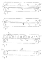
- Figure 1 is a cross section of an arrangement of a device wafer 1 and a carrier 2 during a process step in which the device wafer 1 is separated from the carrier 2.
- a main surface 10 of the device wafer 1 faces a further main surface 20 of the carrier 2.
- the main surface 10 is a surface of a dielectric layer 8, which may comprise a wiring of an integrated circuit of the device wafer 1, for example.
- the dielectric layer 8 may serve as an intermetal dielectric between metal layers forming the wiring.
- the integrated circuit may especially be a CMOS circuit, for example.
- the main surface 10 may instead be formed by a layer of another material, like a passivation layer, or by the surface of a semiconductor body of the device wafer 1.
- the dielectric layer 8 is shown in the described embodiments to indicate that the main surface 10 may be that side of the device wafer 1 where the circuit components are integrated.
- the device wafer 1 may be provided with through-wafer vias 4 and a wiring layer 9 on the surface opposite the carrier 2, for example.
- a recess 5 covering the annular surface region 21 may be provided at the edge of the further main surface 21 for the application of the adhesive 3.
- the device wafer 1 and the carrier 2 have the same dimensions, but the carrier 2 need not have the same dimension as the device wafer 1.
- the area of the further main surface 20 which is fastened to the edge region 11 of the device wafer 1 by means of the adhesive 3 is therefore designated as an annular surface region 21, which is not necessarily on the edge of the carrier 2.
- the adhesive 3 has already partially be removed, so that the device wafer 1 can mechanically be detached from the carrier 2 by applying a moderate force. The residues of the adhesive 3 may then be disposed of when the wafer is diced.
- Figure 2 is a cross section of an arrangement of a device wafer 1 and a carrier 2 before they are fastened to one another.
- the elements that correspond to similar elements shown in Figure 1 are designated with the same reference numerals.
- the carrier 2 is provided with a recess 5, which may be a few microns deep, typically 5 ⁇ m, for instance, and a few millimetres wide, typically 3 mm, for instance.
- An adhesive 3 is dispensed exclusively along the perimeter of the carrier 2.
- the recess 5 enables the application of a sufficiently thick layer of the adhesive 3, which preferably only slightly exceeds the level of the further main surface 21.
- Figure 3 is a cross section according to Figure 2 after the device wafer 1 and the carrier 2 have been fastened to one another. Any surplus adhesive 3 is pushed outwards when the main surface 10 is approached to the further main surface 20. The bond is effected by the adhesive 3 and is confined to the margin of the device wafer 1. Air that may have been trapped in the unbonded central region between the device wafer 1 and the carrier 2 may pose a risk of an uncontrolled delamination of the device wafer 1 from the carrier 2 during further process steps that are performed at a high temperature. This can be avoided if the bonding takes place under low-pressure conditions and/or at an elevated temperature, which typically prevails in wafer bonding chambers. In this way the main surface 10 and the further main surface 20 are brought into contact with one another, while the bond is confined to the periphery.
- the main surface 10 Before the device wafer 1 is fastened to the carrier, the main surface 10 may be provided with a determined roughness in order to prevent the main surface 10 from sticking to the further main surface 20 in an area outside the edge region 11, hence in an area where no adhesive 3 is applied and no bonding is desired. The roughness may facilitate the debonding step.
- the main surface 10 is preferably sufficiently smooth to secure an effective support of the device wafer 1 by the carrier 2, the support being essentially homogeneous over the entire surface.
- FIG 4 is a cross section according to Figure 3 after further process steps.
- the elements that correspond to similar elements shown in Figure 3 are designated with the same reference numerals.
- the device wafer 1 has been thinned from the rear side opposite the carrier 2 and has been provided with through-wafer vias 4 and a wiring layer 9, which may be a redistribution layer, for example.
- the thinned device wafer 1 is mechanically stabilized by the carrier 2 during the further process steps.
- the device wafer 1 can then be removed from the carrier 2.
- the adhesive 3 may be completely removed by a solvent.
- the adhesive 3 may instead be only partially removed by the solvent.
- the boundary of the remaining portion of the adhesive 3 is indicated in Figure 4 by the dotted line traversing the area representing the adhesive 3.
- the rest of the adhesive 3 is sufficient to allow a controlled mechanical detachment of the device wafer 1 from the carrier 2 by an application of a comparatively low force.
- the method step of the mechanical detachment is illustrated in Figure 1 .
- Figure 5 is a cross section according to Figure 2 for a further embodiment.
- the elements that correspond to similar elements shown in Figure 2 are designated with the same reference numerals.
- the adhesive 3 is applied to the device wafer 1. If the edge region 11 of the main surface 10 is left free from the dielectric layer 8, a step 7 is formed at the edge of the dielectric layer 8.
- the step 7 can be used to confine the adhesive 3 to the edge region 11, and the step 7 has a function similar to the function of the recess 5 in the preceding embodiment.
- the adhesive 3 preferably only slightly exceeds the level of the main surface 10.
- Figure 6 is a cross section according to Figure 5 after the device wafer 1 and the carrier 2 have been fastened to one another. Except for the absence of the recess 5 the arrangement shown in Figure 6 equals the arrangement according to Figure 3 . Any surplus adhesive 3 is pushed outwards when the main surface 10 is approached to the further main surface 20. The bond is effected by the adhesive 3 and is confined to the margin of the device wafer 1. The main surface 10 and the further main surface 20 are in contact with one another, while the bond is confined to the periphery.
- Figure 7 is a cross section according to Figure 6 for a further embodiment of the arrangement of the device wafer 1 and the carrier 2.
- the device wafer 1 comprises a high surface topography, which may be due to through-wafer vias 4 that are in this case produced before bonding the device wafer 1 to the carrier.
- the described method does not leave any residues in the region of the high surface topography after debonding, because no adhesive is applied in the central area of the device wafer 1. Cleaning the device wafer 1 is thus not necessary or at least essentially facilitated.
- Figure 8 is a cross section of a further embodiment of the carrier 2, which is here provided with a recess 5 and a further recess 6 in the vicinity of the annular surface region 21 at the edge of the carrier 2.
- the further recess 6 is not filled with the adhesive 3, but it is provided for the accomodation of surplus adhesive 3, which is thus prevented from being squeezed towards the central area of the carrier 2 when the device wafer 1 is fastened.
- the described method enables a temporary bond between a device wafer 1 and a carrier 2 providing an essentially homogeneous support without use of an intermediate layer. Because the bond is effected by an adhesive 3 that is confined to the periphery, the device wafer 1 can easily be detached from the carrier 2, and residues of the adhesive 3 are only left at the margin of the device wafer 1.
- the method allows various adhesives 3 to be selected, including high-temperature stable adhesives 3, so that process steps can be performed at an elevated temperature while the device wafer 1 is supported by the carrier 2.
- the carrier 2 supports the device wafer 1 also in the centre with no need of an intermediate layer.
Landscapes
- Container, Conveyance, Adherence, Positioning, Of Wafer (AREA)
- Mechanical Treatment Of Semiconductor (AREA)
Abstract
Description
- Semiconductor wafers having a thickness of less than 200 µm are particularly suitable for the formation of chip stacks in three-dimensional integration. During manufacture the wafer is fastened to a handling wafer to allow the wafer to be thinned and submitted to further process steps without risk of breaking. The material that fastens the wafer to the handling wafer must be sufficiently inert to chemicals used in the process and must withstand elevated temperatures of typically up to 400°C as well as low-pressure conditions occurring in deposition and cleaning steps. Furthermore, the subsequent removal of the handling wafer must not adversely affect the integrated devices of the semiconductor wafer.
-
US 2008/0014715 A1 discloses a method for the processing of wafers. A device wafer is bonded to a carrier wafer, which supports the device wafer only at its edge, where a bonding substance is applied. After further process steps have been performed, the bonding substance is heated, so that the device wafer can be detached from the carrier wafer. -
US 2009/0218560 A1 discloses a method of production in which a device wafer is bonded to a carrier wafer only at the perimeter. A fill layer surrounded by a material forming an edge bond is arranged between the device wafer and the carrier wafer. The edge bond can be softened, dissolved or mechanically disrupted to allow the wafers to be separated at or near room temperature. - It is an object of this invention to disclose a method of application of a carrier to a device wafer, which provides a good support and facilitates a subsequent removal.
- This object is achieved with the method according to claim 1. Variants derive from the dependent claims.
- The method comprises the steps of providing a device wafer having a main surface including an edge region and providing a carrier having a further main surface including an annular surface region corresponding to the edge region of the device wafer, applying an adhesive in the edge region and/or in the annular surface region, but not on the remaining areas of the main surface and the further main surface, and fastening the device wafer to the carrier by the adhesive. Thereby the main surface is brought into contact with the further main surface inside and outside the edge region, while only the edge region is bonded to the further main surface by the adhesive.
- Further process steps can be performed while the device wafer is supported by the carrier. In particular, further process steps may include the production of through-wafer vias. The device wafer is afterwards removed from the carrier.
- In a variant of the method the device wafer is removed from the carrier by partially removing the adhesive and then mechanically debonding the device wafer from the carrier.
- In a further variant of the method, a recess is formed in the annular surface region of the carrier, and the adhesive is applied in the recess before the device wafer is fastened to the carrier.
- In a further variant of the method, a further recess is formed in the vicinity of the annular surface region of the carrier. The further recess may be provided to accomodate surplus adhesive.
- In a further variant of the method, a step is formed in the edge region of the device wafer, and the adhesive is applied adjacent to the step. The main surface may especially be provided on a dielectric layer, which forms the step.
- In a further variant of the method, the main surface is provided with a roughness preventing the main surface from sticking to the further main surface in an area where no adhesive is applied.
- The following is a detailed description of examples of the semiconductor device and of the appertaining method of production.
- Figure 1
- is a cross section of an arrangement of a device wafer and a carrier during the process of being separated from one another.
- Figure 2
- is a cross section of an arrangement of a device wafer and a carrier before being fastened to one another.
- Figure 3
- is a cross section according to
Figure 2 after the device wafer and the carrier have been fastened to one another. - Figure 4
- is a cross section according to
Figure 3 after further process steps. - Figure 5
- is a cross section according to
Figure 2 for a further embodiment. - Figure 6
- is a cross section according to
Figure 5 after the device wafer and the carrier have been fastened to one another. - Figure 7
- is a cross section according to
Figure 6 for a further embodiment. - Figure 8
- is a cross section of a further embodiment of the carrier.
-
Figure 1 is a cross section of an arrangement of a device wafer 1 and acarrier 2 during a process step in which the device wafer 1 is separated from thecarrier 2. Amain surface 10 of the device wafer 1 faces a furthermain surface 20 of thecarrier 2. In the embodiment shown inFigure 1 , themain surface 10 is a surface of adielectric layer 8, which may comprise a wiring of an integrated circuit of the device wafer 1, for example. Thedielectric layer 8 may serve as an intermetal dielectric between metal layers forming the wiring. The integrated circuit may especially be a CMOS circuit, for example. Themain surface 10 may instead be formed by a layer of another material, like a passivation layer, or by the surface of a semiconductor body of the device wafer 1. Thedielectric layer 8 is shown in the described embodiments to indicate that themain surface 10 may be that side of the device wafer 1 where the circuit components are integrated. The device wafer 1 may be provided with through-wafer vias 4 and a wiring layer 9 on the surface opposite thecarrier 2, for example. - An
adhesive 3, which was used to fasten the device wafer 1 to the carrier, is located in anedge region 11 of themain surface 10 of the device wafer 1 and in a correspondingannular surface region 21 of thecarrier 2. Arecess 5 covering theannular surface region 21 may be provided at the edge of the furthermain surface 21 for the application of theadhesive 3. - In the embodiments shown in the Figures, the device wafer 1 and the
carrier 2 have the same dimensions, but thecarrier 2 need not have the same dimension as the device wafer 1. The area of the furthermain surface 20 which is fastened to theedge region 11 of the device wafer 1 by means of theadhesive 3 is therefore designated as anannular surface region 21, which is not necessarily on the edge of thecarrier 2. - In the state of the method represented in
Figure 1 , theadhesive 3 has already partially be removed, so that the device wafer 1 can mechanically be detached from thecarrier 2 by applying a moderate force. The residues of theadhesive 3 may then be disposed of when the wafer is diced. - The method is further described in conjunction with
Figures 2 to 4. Figure 2 is a cross section of an arrangement of a device wafer 1 and acarrier 2 before they are fastened to one another. The elements that correspond to similar elements shown inFigure 1 are designated with the same reference numerals. At its perimeter, thecarrier 2 is provided with arecess 5, which may be a few microns deep, typically 5 µm, for instance, and a few millimetres wide, typically 3 mm, for instance. Anadhesive 3 is dispensed exclusively along the perimeter of thecarrier 2. Therecess 5 enables the application of a sufficiently thick layer of theadhesive 3, which preferably only slightly exceeds the level of the furthermain surface 21. -
Figure 3 is a cross section according toFigure 2 after the device wafer 1 and thecarrier 2 have been fastened to one another. Anysurplus adhesive 3 is pushed outwards when themain surface 10 is approached to the furthermain surface 20. The bond is effected by theadhesive 3 and is confined to the margin of the device wafer 1. Air that may have been trapped in the unbonded central region between the device wafer 1 and thecarrier 2 may pose a risk of an uncontrolled delamination of the device wafer 1 from thecarrier 2 during further process steps that are performed at a high temperature. This can be avoided if the bonding takes place under low-pressure conditions and/or at an elevated temperature, which typically prevails in wafer bonding chambers. In this way themain surface 10 and the furthermain surface 20 are brought into contact with one another, while the bond is confined to the periphery. - Before the device wafer 1 is fastened to the carrier, the
main surface 10 may be provided with a determined roughness in order to prevent themain surface 10 from sticking to the furthermain surface 20 in an area outside theedge region 11, hence in an area where no adhesive 3 is applied and no bonding is desired. The roughness may facilitate the debonding step. On the other hand, themain surface 10 is preferably sufficiently smooth to secure an effective support of the device wafer 1 by thecarrier 2, the support being essentially homogeneous over the entire surface. -
Figure 4 is a cross section according toFigure 3 after further process steps. The elements that correspond to similar elements shown inFigure 3 are designated with the same reference numerals. The device wafer 1 has been thinned from the rear side opposite thecarrier 2 and has been provided with through-wafer vias 4 and a wiring layer 9, which may be a redistribution layer, for example. The thinned device wafer 1 is mechanically stabilized by thecarrier 2 during the further process steps. The device wafer 1 can then be removed from thecarrier 2. To this end the adhesive 3 may be completely removed by a solvent. The adhesive 3 may instead be only partially removed by the solvent. The boundary of the remaining portion of the adhesive 3 is indicated inFigure 4 by the dotted line traversing the area representing the adhesive 3. The rest of the adhesive 3 is sufficient to allow a controlled mechanical detachment of the device wafer 1 from thecarrier 2 by an application of a comparatively low force. The method step of the mechanical detachment is illustrated inFigure 1 . -
Figure 5 is a cross section according toFigure 2 for a further embodiment. The elements that correspond to similar elements shown inFigure 2 are designated with the same reference numerals. In the embodiment according toFigure 5 the adhesive 3 is applied to the device wafer 1. If theedge region 11 of themain surface 10 is left free from thedielectric layer 8, a step 7 is formed at the edge of thedielectric layer 8. The step 7 can be used to confine the adhesive 3 to theedge region 11, and the step 7 has a function similar to the function of therecess 5 in the preceding embodiment. The adhesive 3 preferably only slightly exceeds the level of themain surface 10. -
Figure 6 is a cross section according toFigure 5 after the device wafer 1 and thecarrier 2 have been fastened to one another. Except for the absence of therecess 5 the arrangement shown inFigure 6 equals the arrangement according toFigure 3 . Anysurplus adhesive 3 is pushed outwards when themain surface 10 is approached to the furthermain surface 20. The bond is effected by the adhesive 3 and is confined to the margin of the device wafer 1. Themain surface 10 and the furthermain surface 20 are in contact with one another, while the bond is confined to the periphery. -
Figure 7 is a cross section according toFigure 6 for a further embodiment of the arrangement of the device wafer 1 and thecarrier 2. In the example shown inFigure 7 the device wafer 1 comprises a high surface topography, which may be due to through-wafer vias 4 that are in this case produced before bonding the device wafer 1 to the carrier. The described method does not leave any residues in the region of the high surface topography after debonding, because no adhesive is applied in the central area of the device wafer 1. Cleaning the device wafer 1 is thus not necessary or at least essentially facilitated. -
Figure 8 is a cross section of a further embodiment of thecarrier 2, which is here provided with arecess 5 and afurther recess 6 in the vicinity of theannular surface region 21 at the edge of thecarrier 2. Thefurther recess 6 is not filled with the adhesive 3, but it is provided for the accomodation ofsurplus adhesive 3, which is thus prevented from being squeezed towards the central area of thecarrier 2 when the device wafer 1 is fastened. - The described method enables a temporary bond between a device wafer 1 and a
carrier 2 providing an essentially homogeneous support without use of an intermediate layer. Because the bond is effected by an adhesive 3 that is confined to the periphery, the device wafer 1 can easily be detached from thecarrier 2, and residues of the adhesive 3 are only left at the margin of the device wafer 1. The method allowsvarious adhesives 3 to be selected, including high-temperaturestable adhesives 3, so that process steps can be performed at an elevated temperature while the device wafer 1 is supported by thecarrier 2. Thecarrier 2 supports the device wafer 1 also in the centre with no need of an intermediate layer. -
- 1
- device wafer
- 2
- carrier
- 3
- adhesive
- 4
- through-wafer via
- 5
- recess
- 6
- further recess
- 7
- step
- 8
- dielectric layer
- 9
- wiring layer
- 10
- main surface
- 11
- edge region
- 20
- further main surface
- 21
- annular surface region
Claims (8)
- A method of application of a carrier, comprising:- providing a device wafer (1) having a main surface (10) including an edge region (11),- providing a carrier (2) having a further main surface (20) including an annular surface region (21) corresponding to the edge region (11),- applying an adhesive (3) to the main surface (10), to the further main surface (20) or both to the main surface (10) and to the further main surface (20) in such a manner that the adhesive (3) is confined to the edge region (11) and to the annular surface region (21), respectively, and- fastening the device wafer (1) to the carrier (2), the adhesive (3) bonding the edge region (11) to the annular surface region (21),
characterized in that- the main surface (10) is brought into contact with the further main surface (20) inside the edge region (11) and outside the edge region (11). - The method of claim 1, wherein
further process steps include the formation of through-wafer vias (4) in the device wafer (1). - The method of claim 1 or 2, wherein
the device wafer (1) is removed from the carrier (2) by partially removing the adhesive (3) and then mechanically debonding the device wafer (1) from the carrier (2). - The method of one of claims 1 to 3, further comprising:forming a recess (5) in the annular surface region (21),andapplying the adhesive (3) in the recess (5).
- The method of claim 4, further comprising:forming a further recess (6) in the vicinity of the annular surface region (21).
- The method of one of claims 1 to 5, further comprising:forming a step (7) in the edge region (11), andapplying the adhesive (3) adjacent to the step (7).
- The method of claim 6, further comprising:providing the main surface (10) on a dielectric layer (8), which forms the step (7).
- The method of one of claims 1 to 7, further comprising:providing the main surface (10) with a roughness preventing the main surface (10) from sticking to the further main surface (20) in an area where no adhesive (3) is applied.
Priority Applications (3)
| Application Number | Priority Date | Filing Date | Title |
|---|---|---|---|
| EP13150530.7A EP2752871B1 (en) | 2013-01-08 | 2013-01-08 | Method of application of a carrier to a device wafer |
| US14/759,400 US20150340264A1 (en) | 2013-01-08 | 2014-01-08 | Method of application of a carrier to a device wafer |
| PCT/EP2014/050233 WO2014108442A1 (en) | 2013-01-08 | 2014-01-08 | Method of application of a carrier to a device wafer |
Applications Claiming Priority (1)
| Application Number | Priority Date | Filing Date | Title |
|---|---|---|---|
| EP13150530.7A EP2752871B1 (en) | 2013-01-08 | 2013-01-08 | Method of application of a carrier to a device wafer |
Publications (2)
| Publication Number | Publication Date |
|---|---|
| EP2752871A1 true EP2752871A1 (en) | 2014-07-09 |
| EP2752871B1 EP2752871B1 (en) | 2015-09-16 |
Family
ID=47605374
Family Applications (1)
| Application Number | Title | Priority Date | Filing Date |
|---|---|---|---|
| EP13150530.7A Active EP2752871B1 (en) | 2013-01-08 | 2013-01-08 | Method of application of a carrier to a device wafer |
Country Status (3)
| Country | Link |
|---|---|
| US (1) | US20150340264A1 (en) |
| EP (1) | EP2752871B1 (en) |
| WO (1) | WO2014108442A1 (en) |
Cited By (1)
| Publication number | Priority date | Publication date | Assignee | Title |
|---|---|---|---|---|
| US11599028B2 (en) | 2017-09-07 | 2023-03-07 | Asml Netherlands B.V. | Methods and systems for clamping a substrate |
Families Citing this family (2)
| Publication number | Priority date | Publication date | Assignee | Title |
|---|---|---|---|---|
| DE102014106100A1 (en) * | 2014-04-30 | 2015-11-05 | Ev Group E. Thallner Gmbh | Method and apparatus for uniforming a substrate stack |
| JP7523983B2 (en) * | 2020-07-22 | 2024-07-29 | キオクシア株式会社 | Semiconductor device and method for manufacturing the same |
Citations (3)
| Publication number | Priority date | Publication date | Assignee | Title |
|---|---|---|---|---|
| US20080014715A1 (en) | 2006-07-13 | 2008-01-17 | Infineon Technologies Ag | Device and method for the processing of wafers |
| WO2009094558A2 (en) * | 2008-01-24 | 2009-07-30 | Brewer Science Inc. | Method for reversibly mounting a device wafer to a carrier substrate |
| US20120193014A1 (en) * | 2011-01-28 | 2012-08-02 | International Business Machines Corporation | Reduction of edge chipping during wafer handling |
Family Cites Families (4)
| Publication number | Priority date | Publication date | Assignee | Title |
|---|---|---|---|---|
| JP2004349649A (en) * | 2003-05-26 | 2004-12-09 | Shinko Electric Ind Co Ltd | Wafer thin processing method |
| JP2007109758A (en) * | 2005-10-12 | 2007-04-26 | Mitsubishi Electric Corp | Method for manufacturing compound semiconductor device |
| JP2013131652A (en) * | 2011-12-21 | 2013-07-04 | Fujitsu Semiconductor Ltd | Semiconductor device manufacturing method, semiconductor wafer processing method, and semiconductor wafer |
| US8580655B2 (en) * | 2012-03-02 | 2013-11-12 | Disco Corporation | Processing method for bump-included device wafer |
-
2013
- 2013-01-08 EP EP13150530.7A patent/EP2752871B1/en active Active
-
2014
- 2014-01-08 US US14/759,400 patent/US20150340264A1/en not_active Abandoned
- 2014-01-08 WO PCT/EP2014/050233 patent/WO2014108442A1/en not_active Ceased
Patent Citations (4)
| Publication number | Priority date | Publication date | Assignee | Title |
|---|---|---|---|---|
| US20080014715A1 (en) | 2006-07-13 | 2008-01-17 | Infineon Technologies Ag | Device and method for the processing of wafers |
| WO2009094558A2 (en) * | 2008-01-24 | 2009-07-30 | Brewer Science Inc. | Method for reversibly mounting a device wafer to a carrier substrate |
| US20090218560A1 (en) | 2008-01-24 | 2009-09-03 | Brewer Science Inc. | Method for reversibly mounting a device wafer to a carrier substrate |
| US20120193014A1 (en) * | 2011-01-28 | 2012-08-02 | International Business Machines Corporation | Reduction of edge chipping during wafer handling |
Cited By (1)
| Publication number | Priority date | Publication date | Assignee | Title |
|---|---|---|---|---|
| US11599028B2 (en) | 2017-09-07 | 2023-03-07 | Asml Netherlands B.V. | Methods and systems for clamping a substrate |
Also Published As
| Publication number | Publication date |
|---|---|
| WO2014108442A1 (en) | 2014-07-17 |
| US20150340264A1 (en) | 2015-11-26 |
| EP2752871B1 (en) | 2015-09-16 |
Similar Documents
| Publication | Publication Date | Title |
|---|---|---|
| JP5351191B2 (en) | Method for producing multilayer structures by trimming using thermo-mechanical effects | |
| US8343851B2 (en) | Wafer temporary bonding method using silicon direct bonding | |
| US10186447B2 (en) | Method for bonding thin semiconductor chips to a substrate | |
| CN103155100B (en) | Multiple Adhesion Layers for Thin Wafer Handling | |
| US20120045611A1 (en) | Composite Carrier Structure | |
| CN103117250B (en) | For the method that carrier is peeled off | |
| CN104064506B (en) | Manufacturing Method For Semiconductor Device | |
| US7795113B2 (en) | Method for bonding a die or substrate to a carrier | |
| JP2004311576A (en) | Method for manufacturing semiconductor device | |
| WO2013136188A1 (en) | Method and apparatus for temporary bonding of ultra thin wafers | |
| US9984888B2 (en) | Method of fabricating a semiconductor wafer including a through substrate via (TSV) and a stepped support ring on a back side of the wafer | |
| JP2017041638A (en) | Underfill film pre-cut and applied to the wafer | |
| EP2752871B1 (en) | Method of application of a carrier to a device wafer | |
| US10749071B2 (en) | Apparatus for processing device structures | |
| US9824912B2 (en) | Method of transforming an electronic device | |
| WO2011134896A2 (en) | Trimming thinning | |
| US9082713B2 (en) | Method of grinding wafer stacks to provide uniform residual silicon thickness | |
| US10163673B2 (en) | Dual adhesive bonding with perforated wafer | |
| US20150279812A1 (en) | Prevention of warping during handling of chip-on-wafer | |
| JP2010062415A (en) | Method of peeling protective tape, and method of manufacturing semiconductor device | |
| WO2004012247A1 (en) | Method for manufacturing semiconductor device | |
| US9362154B2 (en) | Method for treatment of a temporarily bonded product wafer | |
| Dronen et al. | The 3M™ Wafer Support System (WSS) |
Legal Events
| Date | Code | Title | Description |
|---|---|---|---|
| 17P | Request for examination filed |
Effective date: 20130108 |
|
| AK | Designated contracting states |
Kind code of ref document: A1 Designated state(s): AL AT BE BG CH CY CZ DE DK EE ES FI FR GB GR HR HU IE IS IT LI LT LU LV MC MK MT NL NO PL PT RO RS SE SI SK SM TR |
|
| AX | Request for extension of the european patent |
Extension state: BA ME |
|
| PUAI | Public reference made under article 153(3) epc to a published international application that has entered the european phase |
Free format text: ORIGINAL CODE: 0009012 |
|
| R17P | Request for examination filed (corrected) |
Effective date: 20140923 |
|
| RBV | Designated contracting states (corrected) |
Designated state(s): AL AT BE BG CH CY CZ DE DK EE ES FI FR GB GR HR HU IE IS IT LI LT LU LV MC MK MT NL NO PL PT RO RS SE SI SK SM TR |
|
| 17Q | First examination report despatched |
Effective date: 20141021 |
|
| GRAP | Despatch of communication of intention to grant a patent |
Free format text: ORIGINAL CODE: EPIDOSNIGR1 |
|
| INTG | Intention to grant announced |
Effective date: 20150427 |
|
| GRAS | Grant fee paid |
Free format text: ORIGINAL CODE: EPIDOSNIGR3 |
|
| GRAA | (expected) grant |
Free format text: ORIGINAL CODE: 0009210 |
|
| AK | Designated contracting states |
Kind code of ref document: B1 Designated state(s): AL AT BE BG CH CY CZ DE DK EE ES FI FR GB GR HR HU IE IS IT LI LT LU LV MC MK MT NL NO PL PT RO RS SE SI SK SM TR |
|
| REG | Reference to a national code |
Ref country code: GB Ref legal event code: FG4D |
|
| REG | Reference to a national code |
Ref country code: CH Ref legal event code: EP |
|
| REG | Reference to a national code |
Ref country code: IE Ref legal event code: FG4D |
|
| REG | Reference to a national code |
Ref country code: AT Ref legal event code: REF Ref document number: 750394 Country of ref document: AT Kind code of ref document: T Effective date: 20151015 |
|
| REG | Reference to a national code |
Ref country code: DE Ref legal event code: R096 Ref document number: 602013002973 Country of ref document: DE |
|
| REG | Reference to a national code |
Ref country code: NL Ref legal event code: MP Effective date: 20150916 |
|
| PG25 | Lapsed in a contracting state [announced via postgrant information from national office to epo] |
Ref country code: LV Free format text: LAPSE BECAUSE OF FAILURE TO SUBMIT A TRANSLATION OF THE DESCRIPTION OR TO PAY THE FEE WITHIN THE PRESCRIBED TIME-LIMIT Effective date: 20150916 Ref country code: FI Free format text: LAPSE BECAUSE OF FAILURE TO SUBMIT A TRANSLATION OF THE DESCRIPTION OR TO PAY THE FEE WITHIN THE PRESCRIBED TIME-LIMIT Effective date: 20150916 Ref country code: LT Free format text: LAPSE BECAUSE OF FAILURE TO SUBMIT A TRANSLATION OF THE DESCRIPTION OR TO PAY THE FEE WITHIN THE PRESCRIBED TIME-LIMIT Effective date: 20150916 Ref country code: NO Free format text: LAPSE BECAUSE OF FAILURE TO SUBMIT A TRANSLATION OF THE DESCRIPTION OR TO PAY THE FEE WITHIN THE PRESCRIBED TIME-LIMIT Effective date: 20151216 Ref country code: GR Free format text: LAPSE BECAUSE OF FAILURE TO SUBMIT A TRANSLATION OF THE DESCRIPTION OR TO PAY THE FEE WITHIN THE PRESCRIBED TIME-LIMIT Effective date: 20151217 |
|
| REG | Reference to a national code |
Ref country code: LT Ref legal event code: MG4D |
|
| REG | Reference to a national code |
Ref country code: AT Ref legal event code: MK05 Ref document number: 750394 Country of ref document: AT Kind code of ref document: T Effective date: 20150916 |
|
| PG25 | Lapsed in a contracting state [announced via postgrant information from national office to epo] |
Ref country code: RS Free format text: LAPSE BECAUSE OF FAILURE TO SUBMIT A TRANSLATION OF THE DESCRIPTION OR TO PAY THE FEE WITHIN THE PRESCRIBED TIME-LIMIT Effective date: 20150916 Ref country code: HR Free format text: LAPSE BECAUSE OF FAILURE TO SUBMIT A TRANSLATION OF THE DESCRIPTION OR TO PAY THE FEE WITHIN THE PRESCRIBED TIME-LIMIT Effective date: 20150916 Ref country code: SE Free format text: LAPSE BECAUSE OF FAILURE TO SUBMIT A TRANSLATION OF THE DESCRIPTION OR TO PAY THE FEE WITHIN THE PRESCRIBED TIME-LIMIT Effective date: 20150916 |
|
| PG25 | Lapsed in a contracting state [announced via postgrant information from national office to epo] |
Ref country code: NL Free format text: LAPSE BECAUSE OF FAILURE TO SUBMIT A TRANSLATION OF THE DESCRIPTION OR TO PAY THE FEE WITHIN THE PRESCRIBED TIME-LIMIT Effective date: 20150916 |
|
| PG25 | Lapsed in a contracting state [announced via postgrant information from national office to epo] |
Ref country code: IS Free format text: LAPSE BECAUSE OF FAILURE TO SUBMIT A TRANSLATION OF THE DESCRIPTION OR TO PAY THE FEE WITHIN THE PRESCRIBED TIME-LIMIT Effective date: 20160116 Ref country code: IT Free format text: LAPSE BECAUSE OF FAILURE TO SUBMIT A TRANSLATION OF THE DESCRIPTION OR TO PAY THE FEE WITHIN THE PRESCRIBED TIME-LIMIT Effective date: 20150916 Ref country code: EE Free format text: LAPSE BECAUSE OF FAILURE TO SUBMIT A TRANSLATION OF THE DESCRIPTION OR TO PAY THE FEE WITHIN THE PRESCRIBED TIME-LIMIT Effective date: 20150916 Ref country code: SK Free format text: LAPSE BECAUSE OF FAILURE TO SUBMIT A TRANSLATION OF THE DESCRIPTION OR TO PAY THE FEE WITHIN THE PRESCRIBED TIME-LIMIT Effective date: 20150916 Ref country code: CZ Free format text: LAPSE BECAUSE OF FAILURE TO SUBMIT A TRANSLATION OF THE DESCRIPTION OR TO PAY THE FEE WITHIN THE PRESCRIBED TIME-LIMIT Effective date: 20150916 Ref country code: ES Free format text: LAPSE BECAUSE OF FAILURE TO SUBMIT A TRANSLATION OF THE DESCRIPTION OR TO PAY THE FEE WITHIN THE PRESCRIBED TIME-LIMIT Effective date: 20150916 |
|
| PG25 | Lapsed in a contracting state [announced via postgrant information from national office to epo] |
Ref country code: PL Free format text: LAPSE BECAUSE OF FAILURE TO SUBMIT A TRANSLATION OF THE DESCRIPTION OR TO PAY THE FEE WITHIN THE PRESCRIBED TIME-LIMIT Effective date: 20150916 Ref country code: AT Free format text: LAPSE BECAUSE OF FAILURE TO SUBMIT A TRANSLATION OF THE DESCRIPTION OR TO PAY THE FEE WITHIN THE PRESCRIBED TIME-LIMIT Effective date: 20150916 Ref country code: RO Free format text: LAPSE BECAUSE OF FAILURE TO SUBMIT A TRANSLATION OF THE DESCRIPTION OR TO PAY THE FEE WITHIN THE PRESCRIBED TIME-LIMIT Effective date: 20150916 Ref country code: BE Free format text: LAPSE BECAUSE OF NON-PAYMENT OF DUE FEES Effective date: 20160131 Ref country code: PT Free format text: LAPSE BECAUSE OF FAILURE TO SUBMIT A TRANSLATION OF THE DESCRIPTION OR TO PAY THE FEE WITHIN THE PRESCRIBED TIME-LIMIT Effective date: 20160118 |
|
| REG | Reference to a national code |
Ref country code: DE Ref legal event code: R097 Ref document number: 602013002973 Country of ref document: DE |
|
| PLBE | No opposition filed within time limit |
Free format text: ORIGINAL CODE: 0009261 |
|
| STAA | Information on the status of an ep patent application or granted ep patent |
Free format text: STATUS: NO OPPOSITION FILED WITHIN TIME LIMIT |
|
| 26N | No opposition filed |
Effective date: 20160617 |
|
| PG25 | Lapsed in a contracting state [announced via postgrant information from national office to epo] |
Ref country code: DK Free format text: LAPSE BECAUSE OF FAILURE TO SUBMIT A TRANSLATION OF THE DESCRIPTION OR TO PAY THE FEE WITHIN THE PRESCRIBED TIME-LIMIT Effective date: 20150916 Ref country code: LU Free format text: LAPSE BECAUSE OF FAILURE TO SUBMIT A TRANSLATION OF THE DESCRIPTION OR TO PAY THE FEE WITHIN THE PRESCRIBED TIME-LIMIT Effective date: 20160108 |
|
| REG | Reference to a national code |
Ref country code: CH Ref legal event code: PL |
|
| PG25 | Lapsed in a contracting state [announced via postgrant information from national office to epo] |
Ref country code: MC Free format text: LAPSE BECAUSE OF FAILURE TO SUBMIT A TRANSLATION OF THE DESCRIPTION OR TO PAY THE FEE WITHIN THE PRESCRIBED TIME-LIMIT Effective date: 20150916 |
|
| REG | Reference to a national code |
Ref country code: FR Ref legal event code: ST Effective date: 20160930 |
|
| PG25 | Lapsed in a contracting state [announced via postgrant information from national office to epo] |
Ref country code: LI Free format text: LAPSE BECAUSE OF NON-PAYMENT OF DUE FEES Effective date: 20160131 Ref country code: CH Free format text: LAPSE BECAUSE OF NON-PAYMENT OF DUE FEES Effective date: 20160131 |
|
| REG | Reference to a national code |
Ref country code: IE Ref legal event code: MM4A |
|
| PG25 | Lapsed in a contracting state [announced via postgrant information from national office to epo] |
Ref country code: FR Free format text: LAPSE BECAUSE OF NON-PAYMENT OF DUE FEES Effective date: 20160201 Ref country code: SI Free format text: LAPSE BECAUSE OF FAILURE TO SUBMIT A TRANSLATION OF THE DESCRIPTION OR TO PAY THE FEE WITHIN THE PRESCRIBED TIME-LIMIT Effective date: 20150916 |
|
| PG25 | Lapsed in a contracting state [announced via postgrant information from national office to epo] |
Ref country code: BE Free format text: LAPSE BECAUSE OF FAILURE TO SUBMIT A TRANSLATION OF THE DESCRIPTION OR TO PAY THE FEE WITHIN THE PRESCRIBED TIME-LIMIT Effective date: 20150916 |
|
| PG25 | Lapsed in a contracting state [announced via postgrant information from national office to epo] |
Ref country code: IE Free format text: LAPSE BECAUSE OF NON-PAYMENT OF DUE FEES Effective date: 20160108 |
|
| PG25 | Lapsed in a contracting state [announced via postgrant information from national office to epo] |
Ref country code: MT Free format text: LAPSE BECAUSE OF FAILURE TO SUBMIT A TRANSLATION OF THE DESCRIPTION OR TO PAY THE FEE WITHIN THE PRESCRIBED TIME-LIMIT Effective date: 20150916 |
|
| GBPC | Gb: european patent ceased through non-payment of renewal fee |
Effective date: 20170108 |
|
| PG25 | Lapsed in a contracting state [announced via postgrant information from national office to epo] |
Ref country code: GB Free format text: LAPSE BECAUSE OF NON-PAYMENT OF DUE FEES Effective date: 20170108 |
|
| PG25 | Lapsed in a contracting state [announced via postgrant information from national office to epo] |
Ref country code: CY Free format text: LAPSE BECAUSE OF FAILURE TO SUBMIT A TRANSLATION OF THE DESCRIPTION OR TO PAY THE FEE WITHIN THE PRESCRIBED TIME-LIMIT Effective date: 20150916 Ref country code: SM Free format text: LAPSE BECAUSE OF FAILURE TO SUBMIT A TRANSLATION OF THE DESCRIPTION OR TO PAY THE FEE WITHIN THE PRESCRIBED TIME-LIMIT Effective date: 20150916 Ref country code: HU Free format text: LAPSE BECAUSE OF FAILURE TO SUBMIT A TRANSLATION OF THE DESCRIPTION OR TO PAY THE FEE WITHIN THE PRESCRIBED TIME-LIMIT; INVALID AB INITIO Effective date: 20130108 |
|
| PG25 | Lapsed in a contracting state [announced via postgrant information from national office to epo] |
Ref country code: MT Free format text: LAPSE BECAUSE OF FAILURE TO SUBMIT A TRANSLATION OF THE DESCRIPTION OR TO PAY THE FEE WITHIN THE PRESCRIBED TIME-LIMIT Effective date: 20160131 Ref country code: TR Free format text: LAPSE BECAUSE OF FAILURE TO SUBMIT A TRANSLATION OF THE DESCRIPTION OR TO PAY THE FEE WITHIN THE PRESCRIBED TIME-LIMIT Effective date: 20150916 Ref country code: MK Free format text: LAPSE BECAUSE OF FAILURE TO SUBMIT A TRANSLATION OF THE DESCRIPTION OR TO PAY THE FEE WITHIN THE PRESCRIBED TIME-LIMIT Effective date: 20150916 |
|
| PG25 | Lapsed in a contracting state [announced via postgrant information from national office to epo] |
Ref country code: BG Free format text: LAPSE BECAUSE OF FAILURE TO SUBMIT A TRANSLATION OF THE DESCRIPTION OR TO PAY THE FEE WITHIN THE PRESCRIBED TIME-LIMIT Effective date: 20150916 |
|
| PG25 | Lapsed in a contracting state [announced via postgrant information from national office to epo] |
Ref country code: AL Free format text: LAPSE BECAUSE OF FAILURE TO SUBMIT A TRANSLATION OF THE DESCRIPTION OR TO PAY THE FEE WITHIN THE PRESCRIBED TIME-LIMIT Effective date: 20150916 |
|
| P01 | Opt-out of the competence of the unified patent court (upc) registered |
Effective date: 20230822 |
|
| REG | Reference to a national code |
Ref country code: DE Ref legal event code: R079 Ref document number: 602013002973 Country of ref document: DE Free format text: PREVIOUS MAIN CLASS: H01L0021683000 Ipc: H10P0072700000 |
|
| PGFP | Annual fee paid to national office [announced via postgrant information from national office to epo] |
Ref country code: DE Payment date: 20260121 Year of fee payment: 14 |
|
| REG | Reference to a national code |
Ref country code: DE Ref legal event code: R081 Ref document number: 602013002973 Country of ref document: DE Owner name: AMS-OSRAM AG, AT Free format text: FORMER OWNER: AMS AG, UNTERPREMSTAETTEN, AT |