EP2752705A1 - Display device, and television device - Google Patents
Display device, and television device Download PDFInfo
- Publication number
- EP2752705A1 EP2752705A1 EP12827572.4A EP12827572A EP2752705A1 EP 2752705 A1 EP2752705 A1 EP 2752705A1 EP 12827572 A EP12827572 A EP 12827572A EP 2752705 A1 EP2752705 A1 EP 2752705A1
- Authority
- EP
- European Patent Office
- Prior art keywords
- substrate mounting
- mounting member
- region
- substrate
- outer peripheral
- Prior art date
- Legal status (The legal status is an assumption and is not a legal conclusion. Google has not performed a legal analysis and makes no representation as to the accuracy of the status listed.)
- Granted
Links
Images





Classifications
-
- G—PHYSICS
- G02—OPTICS
- G02F—OPTICAL DEVICES OR ARRANGEMENTS FOR THE CONTROL OF LIGHT BY MODIFICATION OF THE OPTICAL PROPERTIES OF THE MEDIA OF THE ELEMENTS INVOLVED THEREIN; NON-LINEAR OPTICS; FREQUENCY-CHANGING OF LIGHT; OPTICAL LOGIC ELEMENTS; OPTICAL ANALOGUE/DIGITAL CONVERTERS
- G02F1/00—Devices or arrangements for the control of the intensity, colour, phase, polarisation or direction of light arriving from an independent light source, e.g. switching, gating or modulating; Non-linear optics
- G02F1/01—Devices or arrangements for the control of the intensity, colour, phase, polarisation or direction of light arriving from an independent light source, e.g. switching, gating or modulating; Non-linear optics for the control of the intensity, phase, polarisation or colour
- G02F1/13—Devices or arrangements for the control of the intensity, colour, phase, polarisation or direction of light arriving from an independent light source, e.g. switching, gating or modulating; Non-linear optics for the control of the intensity, phase, polarisation or colour based on liquid crystals, e.g. single liquid crystal display cells
- G02F1/133—Constructional arrangements; Operation of liquid crystal cells; Circuit arrangements
- G02F1/1333—Constructional arrangements; Manufacturing methods
- G02F1/133308—Support structures for LCD panels, e.g. frames or bezels
-
- H—ELECTRICITY
- H04—ELECTRIC COMMUNICATION TECHNIQUE
- H04N—PICTORIAL COMMUNICATION, e.g. TELEVISION
- H04N5/00—Details of television systems
- H04N5/64—Constructional details of receivers, e.g. cabinets or dust covers
- H04N5/655—Construction or mounting of chassis, e.g. for varying the elevation of the tube
-
- H—ELECTRICITY
- H04—ELECTRIC COMMUNICATION TECHNIQUE
- H04R—LOUDSPEAKERS, MICROPHONES, GRAMOPHONE PICK-UPS OR LIKE ACOUSTIC ELECTROMECHANICAL TRANSDUCERS; ELECTRIC HEARING AIDS; PUBLIC ADDRESS SYSTEMS
- H04R1/00—Details of transducers, loudspeakers or microphones
- H04R1/02—Casings; Cabinets ; Supports therefor; Mountings therein
- H04R1/028—Casings; Cabinets ; Supports therefor; Mountings therein associated with devices performing functions other than acoustics, e.g. electric candles
-
- G—PHYSICS
- G02—OPTICS
- G02F—OPTICAL DEVICES OR ARRANGEMENTS FOR THE CONTROL OF LIGHT BY MODIFICATION OF THE OPTICAL PROPERTIES OF THE MEDIA OF THE ELEMENTS INVOLVED THEREIN; NON-LINEAR OPTICS; FREQUENCY-CHANGING OF LIGHT; OPTICAL LOGIC ELEMENTS; OPTICAL ANALOGUE/DIGITAL CONVERTERS
- G02F1/00—Devices or arrangements for the control of the intensity, colour, phase, polarisation or direction of light arriving from an independent light source, e.g. switching, gating or modulating; Non-linear optics
- G02F1/01—Devices or arrangements for the control of the intensity, colour, phase, polarisation or direction of light arriving from an independent light source, e.g. switching, gating or modulating; Non-linear optics for the control of the intensity, phase, polarisation or colour
- G02F1/13—Devices or arrangements for the control of the intensity, colour, phase, polarisation or direction of light arriving from an independent light source, e.g. switching, gating or modulating; Non-linear optics for the control of the intensity, phase, polarisation or colour based on liquid crystals, e.g. single liquid crystal display cells
- G02F1/133—Constructional arrangements; Operation of liquid crystal cells; Circuit arrangements
- G02F1/1333—Constructional arrangements; Manufacturing methods
- G02F1/133308—Support structures for LCD panels, e.g. frames or bezels
- G02F1/133314—Back frames
-
- G—PHYSICS
- G02—OPTICS
- G02F—OPTICAL DEVICES OR ARRANGEMENTS FOR THE CONTROL OF LIGHT BY MODIFICATION OF THE OPTICAL PROPERTIES OF THE MEDIA OF THE ELEMENTS INVOLVED THEREIN; NON-LINEAR OPTICS; FREQUENCY-CHANGING OF LIGHT; OPTICAL LOGIC ELEMENTS; OPTICAL ANALOGUE/DIGITAL CONVERTERS
- G02F1/00—Devices or arrangements for the control of the intensity, colour, phase, polarisation or direction of light arriving from an independent light source, e.g. switching, gating or modulating; Non-linear optics
- G02F1/01—Devices or arrangements for the control of the intensity, colour, phase, polarisation or direction of light arriving from an independent light source, e.g. switching, gating or modulating; Non-linear optics for the control of the intensity, phase, polarisation or colour
- G02F1/13—Devices or arrangements for the control of the intensity, colour, phase, polarisation or direction of light arriving from an independent light source, e.g. switching, gating or modulating; Non-linear optics for the control of the intensity, phase, polarisation or colour based on liquid crystals, e.g. single liquid crystal display cells
- G02F1/133—Constructional arrangements; Operation of liquid crystal cells; Circuit arrangements
- G02F1/1333—Constructional arrangements; Manufacturing methods
- G02F1/133308—Support structures for LCD panels, e.g. frames or bezels
- G02F1/13332—Front frames
Definitions
- the present invention relates to a display device and a television device, and more particularly, it relates to a display device and a television device each including a display panel including a backlight source.
- a display device and a television device each including a display panel including a backlight source are known in general. Such a display device and a television device are disclosed in National Patent Publication Gazette No. 2009-054177 ( WO2009/054177 ), for example.
- a television receiving device including a front cabinet on a front side, a rear cabinet on a rear side, and a liquid crystal display device stored in a state held between the front cabinet and the rear cabinet.
- This liquid crystal display device includes a bezel on the front side, a liquid crystal panel, and a backlight device on the rear side.
- the backlight device has a frame and a chassis on which a plurality of LED light sources emitting light toward the front side (display side) are arranged.
- Each of the bezel, the frame and the chassis is formed in a rectangular shape having four side surface portions, while the LED light sources are arranged on a region surrounded by the side surface portions of the respective ones of the bezel, the frame and the chassis.
- clearances are formed on corner portions of outer peripheral portions of the respective ones of the bezel, the frame and the chassis.
- Patent Document 1 National Patent Publication Gazette No. 2009-054177
- the present invention has been proposed in order to solve the aforementioned problem, and one object of the present invention is to provide a display device and a television device each capable of inhibiting light of a backlight source from leaking outward through a corner portion.
- a display device includes a display panel including a backlight source and a substrate mounting member covering the backlight source and a cover member arranged to partially cover the rear surface of the substrate mounting member and to expose a region in the periphery of at least an outer peripheral portion of the rear surface of the substrate mounting member, and the substrate mounting member has a bottom surface portion and a side surface portion, while a corner portion of the outer peripheral portion formed by the side surface portion of the substrate mounting member has such a shape that adjacent ones of the side surface portion are bonded to each other without a clearance.
- the corner portion of the outer peripheral portion formed by the side surface portion of the substrate mounting member has such a shape that adjacent ones of the side surface portion are bonded to each other without a clearance, whereby light from the backlight source covered with the substrate mounting member can be inhibited from leaking outward through the corner portion of the substrate mounting member.
- the cover member is arranged to expose the periphery of the outer peripheral portion of the substrate mounting member of the display panel as in the present invention, the light of the backlight source can be reliably inhibited from leaking out of the display device through the corner portion of the exposed outer peripheral portion, due to the corner portion of the substrate mounting member having no clearance.
- the periphery of the outer peripheral portion of the substrate mounting member exposed from the cover member can be easily used as a rear housing by suppressing outward light leakage from the corner portion of the outer peripheral portion of the substrate mounting member.
- an outer peripheral surface of the side surface portion on the corner portion of the substrate mounting member is so formed that adjacent ones of the side surface portion are bonded to each other without a clearance to have a round shape.
- a member other than the substrate mounting member can be inhibited from coming into contact with the corner portion and being damaged dissimilarly to a case where the outer peripheral surface of the corner portion has an angular shape, due to the corner portion of the round shape, while suppressing outward light leakage from the corner portion.
- a rear housing is constituted of the substrate mounting member, and the display device further includes a frame-shaped front housing having an inner peripheral surface approachingly opposed to the outer peripheral surface of the side surface portion of the substrate mounting member.
- the outer peripheral surface of the side surface portion of the substrate mounting member serving also as the rear housing can be covered with the inner peripheral surface of the front housing, whereby the light from the backlight source can be more reliably inhibited from leaking outward through the outer peripheral surface of the side surface portion of the substrate mounting member.
- the inner peripheral surface of the front housing arranged to approach the corner portion can be inhibited from coming into contact with the corner portion and being damaged dissimilarly to a case where the outer peripheral surface of the side surface portion on the corner portion has an angular shape, due to the corner portion of the round shape.
- the front housing includes a light shielding portion formed on a position inward beyond the corner portion of the substrate mounting member to protrude toward the rear surface side.
- the light of the backlight source can be effectively inhibited from leaking out of the display device through the corner portion of the substrate mounting member, due to the light shielding portion.
- the substrate mounting member is made of metal
- the exposed region of the bottom surface portion of the substrate mounting member in the periphery of the outer peripheral portion has a convex shape swelling toward the rear surface side.
- mechanical strength in the periphery of the peripheral portion of the substrate mounting member made of metal can be improved due to the convex shape swelling toward the rear surface side, whereby mechanical strength necessary as the rear housing can be sufficiently ensured also in a case of employing the periphery of the outer peripheral portion of the substrate mounting member exposed from the cover member as the rear housing.
- a region of the bottom surface portion of the substrate mounting member covered with the cover member of the substrate mounting member is formed in a concave shape, and the cover member is mounted to fit into the region of the concave shape.
- the height of the region of the substrate mounting member covered with the cover member decreases due to the formation in the concave shape dissimilarly to a case where the region of the substrate mounting member covered with the cover member is formed in a planar surface shape, whereby the thickness of the whole device can be reduced.
- the aforementioned display device further includes a circuit board mounted on the rear surface of the substrate mounting member, the cover member is arranged to cover the circuit board mounted on the rear surface of the substrate mounting member and to expose a region in the periphery of the outer peripheral portion of the rear surface of the substrate mounting member, the substrate mounting member is made of metal, and the exposed region in the periphery of the outer peripheral portion of the substrate mounting member functions as a heat radiation portion radiating heat of at least the circuit board mounted on the substrate mounting member outward.
- the light of the backlight source can be reliably inhibited from leaking out of the display device through the corner portion of the exposed outer peripheral portion while efficiently radiating the heat from the circuit board mounted on the substrate mounting member made of metal from the exposed region in the periphery of the outer peripheral portion of the substrate mounting member.
- the display device further includes a speaker
- the cover member is arranged to also cover the speaker in addition to the circuit board.
- no member for covering the speaker may be separately provided, whereby the number of components can be reduced.
- the substrate mounting member of the display panel has a substrate mounting region on the rear surface and has a heat radiation function
- the display device further includes a circuit board mounted on the substrate mounting region on the rear surface of the substrate mounting member
- the cover member is arranged to cover the substrate mounting region mounted with the circuit board from behind and to expose a non-substrate-mounting region other than the substrate mounting region on the rear surface of the substrate mounting member
- a rear housing is constituted of at least the exposed non-substrate-mounting region of the substrate mounting member.
- the circuit board mounted on the substrate mounting region of the substrate mounting member can be directly covered with the cover member, whereby no member other than the cover member may be separately provided so that the number of components can be inhibited from increasing. Further, heat generated from the circuit board can be efficiently radiated outward from the exposed non-substrate-mounting region of the substrate mounting member, dissimilarly to a case of covering both of the substrate mounting region and the non-substrate-mounting region of the substrate mounting member with the cover member.
- the rear housing is constituted of at least the exposed non-substrate-mounting region of the substrate mounting member, whereby no rear housing may be separately provided also in a case of arranging the cover member to cover only part (substrate mounting region) of the substrate mounting member.
- the circuit board has an external connection terminal
- the cover member arranged to cover the substrate mounting region and to expose the non-substrate-mounting region has an opening exposing the external connection terminal of the circuit board.
- the external connection terminal of the circuit board can be easily connected with a connection wire of an externally set electronic apparatus or the like through the opening of the cover member.
- the substrate mounting member constituting the rear housing is made of metal, and the exposed non-substrate-mounting region of the substrate mounting member functions as a heat radiation portion radiating heat of at least the circuit board mounted on the substrate mounting region outward.
- the substrate mounting member constituting the rear housing is made of resin, for example, whereby the heat generated from the circuit board can be more efficiently radiated outward.
- the cover member has a recess portion storing the circuit board, and the circuit board mounted on the substrate mounting region on the rear surface of the substrate mounting member is covered with the cover member in a state stored in the recess portion of the cover member.
- the circuit board protruding rearward can be easily stored due to the recess portion of the cover member also in a case where the circuit board is mounted on the rear surface of the substrate mounting member to protrude rearward, whereby the whole circuit board can be easily covered with the cover member.
- the non-substrate-mounting region on the rear surface of the substrate mounting member is provided on the rear surface of the substrate mounting member to surround the periphery of the substrate mounting region.
- the area of the exposed region effective for heat radiation can be enlarged due to the non-substrate-mounting region exposed to surround the periphery of the substrate mounting region of the substrate mounting member, whereby the heat generated from the circuit board mounted on the substrate mounting region of the substrate mounting member can be more effectively radiated.
- the substrate mounting region on the rear surface of the substrate mounting member is formed in a concave shape, and the cover member is mounted to fit into the substrate mounting region of the concave shape.
- the substrate mounting region of the substrate mounting member is so formed in the concave shape that the thickness of the whole device can be reduced, dissimilarly to a case where the substrate mounting region of the substrate mounting member is formed in a planar surface shape.
- the display device further includes a frame-shaped front housing having an inner peripheral surface approaching an outer peripheral surface of the substrate mounting member constituting the rear housing and covering the periphery of the outer peripheral surface.
- the front housing and the rear housing can be easily formed in corresponding shapes by approaching the inner peripheral surface of the front housing to the outer peripheral surface of the substrate mounting member constituting the rear housing.
- the display device further includes a speaker, and the cover member is arranged to also cover the speaker in addition to the circuit board while exposing the non-substrate-mounting region.
- the cover member is arranged to also cover the speaker in addition to the circuit board while exposing the non-substrate-mounting region.
- the cover member is configured to be mountable on the display panel of a different size in a common magnitude.
- no cover member of a different size may be formed to be mounted on a display panel of a different size, whereby manufacturing steps for the cover member can be simplified.
- a television device includes a receiving portion capable of receiving television broadcasting, a display panel including a backlight source and a substrate mounting member covering the backlight source and capable of displaying television broadcasting and a cover member arranged to partially cover the rear surface of the substrate mounting member and to expose a region in the periphery of at least an outer peripheral portion of the rear surface of the substrate mounting member, and the substrate mounting member has a bottom surface portion and a side surface portion, while a corner portion of the outer peripheral portion formed by the side surface portion of the substrate mounting member has such a shape that adjacent ones of the side surface portion are bonded to each other without a clearance.
- the corner portion of the outer peripheral portion formed by the side surface portion of the substrate mounting member has such a shape that adjacent ones of the side surface portion are bonded to each other without a clearance, whereby light from the backlight source covered with the substrate mounting member can be inhibited from leaking outward through the corner portion of the substrate mounting member.
- the cover member is arranged to expose the periphery of the outer peripheral portion of the substrate mounting member of the display panel as in the present invention, the light of the backlight source can be reliably inhibited from leaking out of the television device through the corner portion of the exposed outer peripheral portion, due to the corner portion of the substrate mounting member having no clearance.
- the periphery of the outer peripheral portion of the substrate mounting member exposed from the cover member can be easily used as a rear housing by suppressing outward light leakage from the corner portion of the outer peripheral portion of the substrate mounting member.
- an outer peripheral surface of the side surface portion on the corner portion of the substrate mounting member is so formed that adjacent ones of the side surface portion are bonded to each other without a clearance to have a round shape.
- a member other than the substrate mounting member can be inhibited from coming into contact with the corner portion and being damaged dissimilarly to a case where the outer peripheral portion of the corner portion has an angular shape, due to the corner portion of the round shape.
- the substrate mounting member of the display panel has a substrate mounting region on the rear surface and has a heat radiation function
- the television device further includes a circuit board mounted on the substrate mounting region on the rear surface of the substrate mounting member
- the cover member is arranged to cover the substrate mounting region mounted with the circuit board from behind and to expose a non-substrate-mounting region other than the substrate mounting region on the rear surface of the substrate mounting member
- a rear housing is constituted of at least the exposed non-substrate-mounting region of the substrate mounting member.
- the circuit board mounted on the substrate mounting region of the substrate mounting member can be directly covered with the cover member, whereby no member other than the cover member may be separately provided so that the number of components can be inhibited from increasing. Further, heat generated from the circuit board can be efficiently radiated outward from the exposed non-substrate-mounting region of the substrate mounting member, dissimilarly to a case of covering both of the substrate mounting region and the non-substrate-mounting region of the substrate mounting member with the cover member.
- the rear housing is constituted of at least the exposed non-substrate-mounting region of the substrate mounting member, whereby no rear housing may be separately provided also in a case of arranging the cover member to cover only part (substrate mounting region) of the substrate mounting member.
- the light of the backlight source can be inhibited from leaking outward through the corner portion.
- the structure of a liquid crystal television device 100 according to the embodiment of the present invention is described with reference to Figs. 1 to 19 .
- the liquid crystal television device 100 is an example of the "display device” and the “television device” in the present invention.
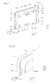
- the liquid crystal television device 100 has a rectangular shape, and includes a frame-shaped front housing 1, a liquid crystal module 2 stored in the front housing 1, and a stand member 3 (see Fig. 2 ) supporting the whole liquid crystal television device 100, as shown in Figs. 1 and 2 .
- the liquid crystal module 2 is an example of the "display panel" in the present invention.
- the front housing 1 and the stand member 3 are both made of resin.
- a rear frame 5 made of metal consisting of sheet metal is arranged on a rear surface side (Y2 side, see Fig. 2 ) of the front housing 1.
- the rear frame 5 is an example of the "substrate mounting member" in the present invention.
- the rear frame 5 has a rectangular shape as viewed from behind (Y2 side), and is formed to be smaller than the front housing 1.
- an inner peripheral surface 101a of a peripheral edge portion 1a of the front housing 1 is configured to approach (to come into contact with) outer peripheral surfaces 51i, described later, of the rear frame 5 and to cover the outer peripheral surfaces 51i of the rear frame 5.
- One cover member 6 made of resin is mounted on a back surface (rear surface) side (Y2 side, see Fig. 4 ) of the rear frame 5 made of sheet metal.
- This cover member 6 has a rectangular shape as viewed from behind (Y2 side), and is formed to be smaller than the front housing 1 and the rear frame 5.
- components such as a light reflection sheet (not shown), a light guide (not shown), an optical sheet (not shown), a frame-shaped resin frame 4a, a liquid crystal cell (not shown) and a frame-shaped bezel (not shown) are arranged between the front housing 1 and the rear frame 5 from the rear frame 5 toward the direction (arrow Y1 direction) of the front housing 1.
- a light source 4b constituted of a plurality of LEDs is arranged on a side portion on an X2 side of the resin frame 4a.
- the light source 4b is an example of the "backlight source" in the present invention.
- the liquid crystal module 2 includes the resin frame 4a, the aforementioned unshown components, the light source 4b and the rear frame 5.
- the rear frame 5 includes a bottom surface portion 50 formed in a substantially rectangular shape and four side surface portions 51a, 51b, 51c and 51d positioned on an outer peripheral portion 51 of the rear frame 5 and extending from the bottom surface portion 50 toward the front side (Y1 side, see Fig. 6 ), as shown in Figs. 5 to 7 .
- These four side surface portions 51a to 51d are formed by such an operation that portions of the bottom surface portion 50 in the vicinity of the outer peripheral portion 51 are bent in a direction (Y1 side) perpendicular to the bottom surface portion 50 when forming the rear frame 5 by drawing press working.
- the side surface portions 51a to 51d of the rear frame 5 are formed to extend over the whole periphery of the outer peripheral portion 51 of the rear frame 5, while corner portions 51e, 51f, 51g and 51h on four corners of the outer peripheral portion 51 are all configured to be exposed outward.
- the adjacent pair of side surface portions 51a and 51b are bonded to each other without a clearance on the corner portion 51e of the outer peripheral portion 51. More specifically, an X1-side end portion of the side surface portion 51a linearly extending in an X direction and a Z1-side end portion of the side surface portion 51b linearly extending in a Y direction are integrally connected with each other by the corner portion 51e without a clearance, as shown in Figs. 8 and 9 . Further, the outer peripheral surface 51i on the corner portion 51e is formed to have a round shape (curved surface shape) of a prescribed radius R of curvature (see Fig. 9 ). The corner portion 51e is integrally formed simultaneously with the pair of side surface portions 51a and 51b when forming the rear frame 5 by drawing press working.
- the adjacent pair of side surface portions 51b and 51c are integrally connected with each other without a clearance on the corner portion 51f, as shown in Figs. 5 to 7 .
- the adjacent pair of side surface portions 51c and 51d are integrally connected with each other without a clearance on the corner portion 51g.
- the adjacent pair of side surface portions 51d and 51a are integrally connected with each other without a clearance on the corner portion 51h.
- the outer peripheral surfaces 51i on the corner portions 51f to 51h are all formed to have round shapes of the prescribed radius R of curvature.
- the corner portions 51f to 51h are integrally formed simultaneously with the side surface portions 51a to 51d when forming the rear frame 5 by drawing press working.
- a projecting portion 50a swelling toward the rear side (Y2 side) is formed on a non-substrate-mounting region 50d (region of the rear frame 5 exposed from the cover member 6), described later, of the bottom surface portion 50 of the rear frame 5 in the vicinity of the outer peripheral portion 51.
- This projecting portion 50a is formed to gradually swell toward the rear side (Y2 side) from the vicinity of the side surface portions 51a, 51b and 51d.
- the bottom surface 50 is so concaved toward the front side (Y1 side) that a recess portion 50c formed in a concave shape as a whole is formed on a substrate mounting region 50b on an inner side (central side) of a region of the bottom surface portion 50 where the projecting portion 50a is formed.
- the projecting portion 50a and the recess portion 50c of the bottom surface portion 50 of the rear frame 5 are integrally formed by drawing press working.
- a circuit board 7 having a function of supplying power to the whole device and a circuit board 8 for signal processing are alignedly mounted on the rear surface of the substrate mounting region 50b consisting of the recess portion 50c of the bottom surface portion 50 of the rear frame 5 at a prescribed interval in the X direction.
- the rear surface of the rear frame 5 includes the substrate mounting region 50b provided on a central portion so that the two circuit boards 7 and 8 are mounted thereon and the non-substrate-mounting region 50d provided to surround the periphery of the substrate mounting region 50b and consisting of a region other than the substrate mounting region 50b, as shown in Figs. 6 and 7 .
- a plurality of substrate mounting threaded holes 50e for mounting the respective ones of the two circuit boards 7 and 8 are formed on the substrate mounting region 50b (rear surface of the rear frame 5) consisting of the recess portion 50c. These substrate mounting threaded holes 50e are provided on portions protruding toward the rear side (Y2 side) beyond the substrate mounting region 50b consisting of the recess portion 50c.
- screw insertion holes 7a for inserting screws 9 thereinto are formed on an outer edge portion of the circuit board 7, while screw insertion holes 8a for inserting the screws 9 thereinto are formed on an outer edge portion of the circuit board 8.
- the plurality of screws 9 are mounted on the plurality of substrate mounting threaded holes 50e of the rear frame 5 through the screw insertion holes 7a of the circuit board 7 and the screw insertion holes 8a of the circuit board 8, whereby the respective ones of the two circuit boards 7 and 8 are fixed to the rear frame 5.
- a plurality of screw insertion holes 50f are formed along the outer peripheral portion 51 of the bottom surface portion 50 (rear surface of the rear frame 5) of the rear frame 5.
- the respective ones of the plurality of screws 9 are mounted on the plurality of screw insertion holes 50f (see Fig. 5 ), whereby the rear frame 5 is mounted on the front housing 1.
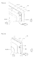
- the liquid crystal television device 100 is so configured that the rear frame 5 is fitted into the front housing 1 so that the inner peripheral surface 101a of the front housing 1 approaches the outer peripheral portion 51 of the rear frame 5 and is opposed to the outer peripheral surfaces 51i of the outer peripheral portion 51 at this time, as shown in Figs. 13 to 15 .
- the outer peripheral surfaces 51i of the corner portions 51e and 51f (see Fig. 3 ) of the rear frame 5 have the round shapes, whereby it is possible to easily arrange the corner portions 51e and 51f of the rear frame 5 on corner portions of the front housing 1.
- rail portions 1b between which the side surface portions 51a, 51b and 51d of the rear frame 5 are held are formed on portions of the peripheral edge portion 1a of the front housing 1 opposed to the side surface portions 51a, 51b and 51d of the rear frame 5 respectively.
- the liquid crystal television device 100 is so configured that the rear frame 5 is positioned on the front housing 1 by the rail portions 1b.
- outer-side inner side surfaces (X1-side inner side surface in Fig. 10 , for example) are configured to become the inner peripheral surface 101a of the peripheral edge portion 1a of the front housing 1.
- no rail portions 1b are formed on portions of the peripheral edge portion 1a of the front housing 1 opposed to the corner portions 51e and 51h on the upper side (Z1 side) of the rear frame 5.
- ribs 1c are provided in the vicinity of the corner portions of the front housing 1 corresponding to the corner portions 51e and 51h respectively. This pair of ribs 1c are formed on inner sides (resin frame 4a sides) beyond the peripheral edge portion 1a of the front housing 1 and the corner portions 51e and 51h of the rear frame 5 respectively.
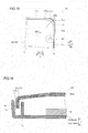
- the pair of ribs 1c are formed to protrude toward the rear surface side up to projection height positions slightly lower than projection heights toward the rear surface side (Y2 side) of the peripheral edge portion 1a, as shown in Fig. 16 .
- the pair of ribs 1c are formed in curved surface shapes to correspond to the corner portions 51e and 51h (see Fig. 3 ) respectively, as shown in Fig. 15 .
- the pair of ribs 1c are configured to effectively inhibit light from the light source 4 from reaching the corner portions 51e and 51h of the rear frame 5 respectively.
- the ribs 1c are examples of the "light shielding portion" in the present invention.
- the peripheral edge portion 1a of the front housing 1 and the corner portions 51e and 51h (see Fig. 3 ) of the rear frame 5 are arranged not to come into contact with each other. Thus, it is possible to inhibit the peripheral edge portion 1a from coming into contact with the corner portions 51e and 51h and being damaged.
- a plurality of cover member mounting threaded holes 50g are formed on the rear surface (Y2 side) of the bottom surface portion 50 of the rear frame 5, while a plurality of screw insertion holes 6a and 61a are formed on the cover member 6.
- the screws 9 are mounted on the respective ones of the plurality of screw insertion holes 6a and 61a, whereby the cover member 6 made of resin is mounted on the rear frame 5 made of metal. More specifically, the screws 9 are mounted on the cover member mounting threaded holes 50g of the rear frame 5 through the screw insertion holes 6a of the cover member 6, whereby the cover member 6 is fixed to the rear frame 5.
- the screw 9 inserted into the screw insertion hole 61a formed on the upper left side of the cover member 6 is mounted on the substrate mounting threaded hole 50a formed on the upper left side of the rear frame 5 through the screw insertion hole 7a formed on the upper left side of the circuit board 7.
- the cover member 6 is mounted on the cover member mounting threaded holes 50g formed on the lower side (Z2 side) among the cover member mounting threaded holes 50g formed on the rear surface of the rear frame 5 through the screws 9, to hold a speaker mounting member 10 therebetween.
- Two speakers 11 are mounted on the speaker mounting member 10.
- the cover member 6 is mounted to cover the two circuit boards 7 and 8 and the speaker mounting member 10 mounted with the two speakers 11 from behind (Y2 side).
- the cover member 6 is arranged to cover left, right and upper edge portions of the substrate mounting region 50b of the bottom surface portion 50 of the rear frame 5 mounted with the two circuit boards 7 and 8 from behind (Y2 side) and to expose the non-substrate-mounting region 50d on the rear surface (Y2 side) of the rear frame 5.
- No non-substrate-mounting region 50d is provided on a lower edge portion side (Z2 side) of the substrate mounting region 50b of the rear frame 5.
- the non-substrate-mounting region 50d of the rear frame 5 exposed from the cover member 6 has an inverted U shape (see Fig. 3 ).
- a rear housing of the liquid crystal television device 100 is constituted of the inverted U-shaped non-substrate-mounting region 50d in the vicinity of the exposed outer peripheral portion 51 of the rear frame 5 made of metal (sheet metal).
- a portion of the rear frame 5 made of metal constituting the liquid crystal module 2 exposed from the cover member 6 is employed also as the rear housing in this embodiment.
- the rear housing is constituted of the non-substrate-mounting region 50d of the rear frame 5 made of metal and the cover member 6.
- the exposed inverted U-shaped non-substrate-mounting region 50d of the rear frame 5 made of metal is configured to function as a heat radiation portion radiating heat generated from the circuit boards 7 and 8 mounted on the substrate mounting region 50b (see Fig. 5 ) outward.
- an inner peripheral edge portion of the recess portion 50c constituting the substrate mounting region 50b of the bottom surface portion 50 is formed to correspond to the outer peripheral portion of the cover member 6.
- the cover member 6 has a recess portion 6b storing the two circuit boards 7 and 8 mounted on the substrate mounting region 50 on the rear surface of the rear frame 5.
- This recess portion 6b of the cover member 6 has a shape concaved rearward (in an arrow Y2 direction).
- the two circuit boards 7 and 8 are stored in the recess portion 6b of the cover member 6, and covered with the cover member 6 in a state separating from the inner surface of the cover member 6.
- end portions 6e of the cover member 6 are fitted into the inner peripheral edge portion of the recess portion 50c of the bottom surface portion 50 from the Y2 side, whereby the cover member 6 in a state covering the recess portion 50c (substrate mounting region 50b) is mounted to fit into the bottom surface portion 50 (substrate mounting region 50b) of the rear frame 5.
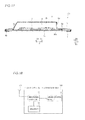
- the circuit board 8 for signal processing arranged on the X1 side in the two circuit boards 7 and 8 mounted on the rear frame 5 has external connection terminals 12a and 12b and a receiving portion (tuner) 13, capable of receiving television broadcasting, connected with the external connection terminal 12b.
- the receiving portion 13 is connected with the liquid crystal module 2 and the speakers 11, and configured to output a picture signal to the liquid crystal module 2 and to output a sound signal to the speakers 11 in television broadcasting signals (the picture signal and the sound signal) received by the antenna 101, as shown in Fig. 18 .
- the external connection terminals 12a are provided on the circuit board 8 to protrude from the circuit board 8 toward the rear surface (Y2 side), while the external connection terminal 12b is provided on the circuit board 8 to protrude from the circuit board 8 toward a side portion (X1 side).
- FIG. 19 six openings 6c having round hole shapes for exposing the external connection terminals 12a provided on the circuit board 8 rearward (in the arrow Y2 direction) are provided on the rear surface of the cover member 6.
- the six external connection terminals 12a provided on the circuit board 8 are configured to be connectable with connection wires of an externally provided electronic apparatus or the like through the six openings 6c of the cover member 6 respectively.
- the cover member 6 has an opening 6d for exposing the external connection terminal 12b provided on the circuit board 8 toward the side portion (arrow X1 direction). This opening 6d has a rectangular shape extending in the vertical direction (Z direction) as viewed from the side portion (X direction).
- the cover member 6 of one size is configured to be mountable on the rear frames 5 and 105 of different sizes.
- a liquid crystal television device shown in Fig. 20 is a 19-inch one (19 inches)
- a liquid crystal television device shown in Fig. 21 is a 22-inch one (22 inches)
- the surface area of a non-substrate-mounting region 50d of a rear frame of the 22-inch liquid crystal television device becomes larger than the surface area of a non-substrate-mounting region 50d of the 19-inch liquid crystal television device. It is also possible to mount a cover member of a size common to 26 inches and 32 inches on a 26-inch liquid crystal television device and a 32-inch liquid crystal television device, for example, in addition to the operation of mounting the cover member 6 of the same size on the 19-inch liquid crystal television device and the 22-inch liquid crystal television device.
- light from the light source 4b covered with the rear frame 5 can be inhibited from leaking outward through the corner portions 51e to 51h of the rear frame 5 by configuring the liquid crystal television device 100 so that the adjacent pairs of side surface portions 51a to 51d are integrally connected with each other without clearances on the corner portions 51e to 51h.
- the cover member 6 is arranged to expose the periphery of the outer peripheral portion 51 of the rear frame 5 of the liquid crystal module 2 as in this embodiment, the light of the light source 4b can be reliably inhibited from leaking out of the liquid crystal television device 100 through the corner portions 51e to 51h of the exposed outer peripheral portion 51, due to the corner portions 51e to 51h of the rear frame 5 having no clearances. Further, the periphery of the outer peripheral portion 51 of the rear frame 5 exposed from the cover member 6 can be easily used as the rear housing by suppressing outward light leakage from the corner portions 51e to 51h of the outer peripheral portion 51 of the rear frame 5.
- the outer peripheral surfaces 51i on the corner portions 51e to 51h are formed to have the round shapes of the prescribed radius R of curvature respectively.
- the inner peripheral surface 101a of the front housing 1 arranged to approach the corner portions 51e to 51h can be inhibited from coming into contact with the corner portions 51e to 51h and being damaged dissimilarly to a case where the outer peripheral surfaces 51i of the corner portions 51e to 51h have angular shapes, due to the round-shaped corner portions 51e to 51h, while suppressing outward light leakage from the corner portions 51e to 51h.
- the rear frame 5 is configured to be fitted into the front housing 1, so that the inner peripheral surface 101a of the peripheral edge portion 1a of the front housing 1 approaches the outer peripheral portion 51 of the rear frame 5 and is opposed to the outer peripheral surfaces 51i of the outer peripheral portion 51.
- the outer peripheral surfaces 51i of the side surface portions 51a to 51d of the rear frame 5 serving also as the rear housing can be covered with the inner peripheral surface 101a of the front housing 1, whereby the light from the light source 4b can be more reliably inhibited from leaking outward through the outer peripheral surfaces 51i of the side surface portions 51a to 51d of the rear frame 5.
- the pair of ribs 1c are formed on the inner side (resin frame 4a side) beyond the corner portions 51e and 51h of the rear frame 5 respectively. Further, the pair of ribs 1c are formed to protrude toward the rear surface side (Y2 side), and formed in the curved surface shapes to correspond to the corner portions 51e and 51h respectively.
- the light of the light source 4b can be effectively inhibited from leaking out of the liquid crystal television device 100 through the corner portions 51e and 51h of the rear frame 5, due to the pair of ribs 1c.
- the projecting portion 50a swelling toward the rear side (Y2 side) beyond the remaining region (region in the vicinity of the side surface portions 51a, 51b and 51d of the outer peripheral portion 51) on the region of the bottom surface portion 50 of the rear frame 5 made of metal excluding the vicinity of the side surface portions 51a, 51b and 51d of the outer peripheral portion 51.
- mechanical strength in the periphery of the outer peripheral portion 51 of the rear frame 5 made of metal can be improved due to the convex shape swelling toward the rear surface side (Y2 side), whereby mechanical strength necessary as the rear housing can be sufficiently ensured also in the case of employing the periphery of the outer peripheral portion 51 of the rear frame 5 exposed from the cover member 6 as the rear housing.
- the liquid crystal television device 100 is so configured that the cover member 6 is fitted into the recess portion 50c of the bottom surface portion 50 from the Y2 side, so that the cover member 6 is mounted on the bottom surface portion 50 of the rear frame 5 in the state covering the recess portion 50c.
- the height of the recess portion 50c of the rear frame 5 decreases due to the formation in the concave shape dissimilarly to a case where the region (recess portion 50c) of the rear frame 5 covered with the cover member 6 is formed in a planar surface shape, whereby the thickness of the whole device can be reduced.
- positioning of the cover member 6 can be easily performed by fitting the cover member 6 into the recess portion 50c of the bottom surface portion 5 from the Y2 side.
- the liquid crystal television device 100 is so configured that the cover member 6 covers the recess portion 50c of the bottom portion 50 of the rear frame 5 mounted with the two circuit boards 7 and 8 from behind (Y2 side) so that the side surface portions 51a, 51b and 51c of the rear surface of the rear frame 5 are exposed, and so configured that a portion of the rear frame 5 made of metal in the vicinity of the exposed outer peripheral portion 51 functions as the heat radiation portion radiating the heat generated from the circuit boards 7 and 8 mounted on the recess portion 50c outward.
- the light of the light source 4b can be reliably inhibited from leaking out of the liquid crystal television device 100 through the corner portions 51e to 51h of the exposed outer peripheral portion 51 while efficiently radiating the heat from the circuit boards 7 and 8 mounted on the rear frame 5 made of metal from a region in the periphery of the exposed outer peripheral portion 51 of the rear frame 5 outward.
- the cover member 6 is mounted on the rear surface (Y2 side) of the rear frame 5, to cover the two circuit boards 7 and 8 and the two speakers 11.
- no member for covering the speakers 11 may be separately provided, whereby the number of components can be reduced.
- the cover member 6 is arranged to cover the substrate mounting region 50b mounted with the circuit boards 7 and 8 on the rear surface from behind and to expose the non-substrate-mounting region 50d of the rear surface of the rear frame 5 other than the substrate mounting region 50b.
- the circuit boards 7 and 8 mounted on the substrate mounting region 50b of the rear frame 5 can be directly covered with the cover member 6, whereby no member other than the cover member 6 may be separately provided, so that the number of components can be inhibited from increasing.
- the heat generated from the circuit boards 7 and 8 can be efficiently radiated outward from the exposed non-substrate-mounting region 50d of the rear frame 5, dissimilarly to a case of covering both of the substrate mounting region 50b and the non-substrate-mounting region 50d of the rear frame 5 with the cover member 6.
- the rear housing is constituted of the exposed non-substrate mounting region 50d of the rear frame 5, whereby no rear housing may be separately provided also in the case of arranging the cover member 6 to cover only part (substrate mounting region 50b) of the rear frame 5.
- the cover member 6 arranged to cover the substrate mounting region 50b and to expose the non-substrate-mounting region 50d has the openings 6c exposing the six external connection terminals 12a of the circuit board 8 and the opening 6d exposing the external connection terminal 12b.
- the external connection terminals 12a and 12b of the circuit board 8 can be easily connected with connection wires of an externally provided electronic apparatus or the like through the openings 6c and 6d of the cover member 6 in the state where the circuit boards 7 and 8 are covered with the cover member 6.
- the rear frame 5 constituting the rear housing is made of metal while the exposed non-substrate-mounting region 50d of the rear frame 5 is made to function as the heat radiation portion radiating the heat of the circuit boards 7 and 8 mounted on the substrate mounting region 50b outward so that heat is more easily transferred as compared with a case where the rear frame 5 constituting the rear housing is made of resin, whereby the heat generated from the circuit boards 7 and 8 can be more efficiently radiated outward.
- the circuit boards 7 and 8 mounted on the substrate mounting region 50b of the rear surface of the rear frame 5 are covered with the cover member 6 in the state stored in the recess portion 6b of the cover member 6.
- the circuit boards 7 and 8 protruding rearward can be easily stored due to the recess portion 6b of the cover member 6 also in the case where the circuit boards 7 and 8 are mounted on the rear surface of the rear frame 5 to protrude rearward, whereby the whole circuit boards 7 and 8 can be easily covered with the cover member 6.
- the non-substrate-mounting region 50d is provided on the rear surface of the rear frame 5 to surround the periphery of the substrate mounting region 50b so that the area of the exposed region effective for heat radiation can be enlarged due to the non-substrate-mounting region 50d exposed to surround the periphery of the substrate mounting region 50b of the rear frame 5, whereby the heat generated from the circuit boards 7 and 8 mounted on the substrate mounting region 50b of the rear frame 5 can be more effectively radiated.
- the cover member 6 is mounted to fit into the substrate mounting region 50b of the concave shape, whereby the substrate mounting region 50b of the rear frame 5 is so formed in the concave shape that the thickness of the whole liquid crystal television device 100 can be reduced, dissimilarly to a case where the substrate mounting region 50b of the rear frame 5 is formed in a planar surface shape.
- the frame-shaped front housing 1 having the inner peripheral surface 101a covering the periphery of the outer peripheral portion 51 to approach the outer peripheral portion 51 of the rear frame 5 constituting the rear housing, whereby the front housing 1 and the rear housing (rear frame 5) can be easily formed in corresponding shapes by making the inner peripheral surface 101a of the front housing 1 approach the outer peripheral portion 51 of the rear frame 5 constituting the rear housing.
- the cover member 6 is arranged to also cover the speakers 11 in addition to the circuit boards 7 and 8 while exposing the non-substrate-mounting region 50d, whereby no member for covering the speakers 11 may be separately provided so that increase in the number of components can be suppressed.
- the cover member 6 is configured to be mountable on display panels 2 (rear frames 5 and 105) of different sizes (19 inches, 22 inches and the like) in a common magnitude (size) so that it is not necessary to form cover members 6 of different magnitudes (sizes) to be mounted on the display panels 2 (rear frames 5 and 105) of different sizes (19 inches, 22 inches and the like), whereby manufacturing steps for the cover member 6 can be simplified.
- the present invention is not restricted to this. According to the present invention, only at least one portion and not more than three portions of the four corner portions 51e to 51h may be exposed outward. In this case, adjacent side surface portions may not be bonded to each other without a clearance on the corner portion(s) not exposed outward.
- the present invention is not restricted to this.
- the corner portions and the side surface portions may not be simultaneously integrally formed.
- the liquid crystal television device may be so configured that the adjacent side surface portions are bonded to each other without clearances on the corner portions by previously forming the side surface portions in a state separating from each other by press working or the like and thereafter bonding the side surface portions in the separating state to each other by employing a bonding method such as welding.
- the rear frame 5 is made of metal consisting of sheet metal
- the present invention is not restricted to this.
- the rear frame may be configured to consist of another material such as resin.
- the rear frame is preferably made of metal excellent in thermal conductivity.
- the present invention is not restricted to this.
- the shapes of the outer peripheral surfaces of the corner portions are not particularly restricted, so far as the adjacent side surface portions are bonded to each other by the corner portions without clearances.
- the outer peripheral surfaces of the corner portions may have C chamfered shapes or angular shapes.
- both of a rib 1c and a rail portion 201b may be provided in the vicinity of a corner portion of a front housing 201 corresponding to a corner portion 51e, as in a modification shown in Fig. 22 .
- the liquid crystal television device 200 is an example of the "display device” and the “television device” in the present invention.
- the present invention is not restricted to this.
- the present invention is applicable also to another display device, such as a monitor of a personal computer, for example, other than the television device or a television device other than the liquid crystal television device.
- the present invention is not restricted to this.
- a substrate mounting member other than the rear frame is also applicable, if it is possible to cover a substrate mounting region mounted with a circuit board with a cover member.
- cover member made of resin as an example of the cover member in the present invention
- cover member made of metal may be employed.
- the present invention is not restricted to this.
- one or at least three circuit boards may be mounted on the substrate mounting region of the rear frame.
- the cover member is recommendably arranged to cover the circuit board(s) in the number of one or at least three mounted on the substrate mounting region of the rear frame.
Landscapes
- Physics & Mathematics (AREA)
- Nonlinear Science (AREA)
- Engineering & Computer Science (AREA)
- Signal Processing (AREA)
- Chemical & Material Sciences (AREA)
- Mathematical Physics (AREA)
- Crystallography & Structural Chemistry (AREA)
- General Physics & Mathematics (AREA)
- Optics & Photonics (AREA)
- Acoustics & Sound (AREA)
- Multimedia (AREA)
- Devices For Indicating Variable Information By Combining Individual Elements (AREA)
- Liquid Crystal (AREA)
Description
- The present invention relates to a display device and a television device, and more particularly, it relates to a display device and a television device each including a display panel including a backlight source.
- A display device and a television device each including a display panel including a backlight source are known in general. Such a display device and a television device are disclosed in National Patent Publication Gazette No.
2009-054177 (WO2009/054177 ), for example. - In National Patent Publication Gazette No. 2009-054177, there is disclosed a television receiving device including a front cabinet on a front side, a rear cabinet on a rear side, and a liquid crystal display device stored in a state held between the front cabinet and the rear cabinet. This liquid crystal display device includes a bezel on the front side, a liquid crystal panel, and a backlight device on the rear side. The backlight device has a frame and a chassis on which a plurality of LED light sources emitting light toward the front side (display side) are arranged. Each of the bezel, the frame and the chassis is formed in a rectangular shape having four side surface portions, while the LED light sources are arranged on a region surrounded by the side surface portions of the respective ones of the bezel, the frame and the chassis. According to National Patent Publication Gazette No.
2009-054177 , clearances are formed on corner portions of outer peripheral portions of the respective ones of the bezel, the frame and the chassis. - Patent Document 1: National Patent Publication Gazette No.
2009-054177 - In the television receiving device described in National Patent Publication Gazette No.
2009-054177 , however, the clearances are formed on the corner portions of the outer peripheral portions of the respective ones of the bezel, the frame and the chassis, and hence there is such a problem that the light from the LED light sources leaks out of the liquid crystal display device through clearances on respective ones of corner portions of the liquid crystal display device. - The present invention has been proposed in order to solve the aforementioned problem, and one object of the present invention is to provide a display device and a television device each capable of inhibiting light of a backlight source from leaking outward through a corner portion.
- A display device according to a first aspect of the present invention includes a display panel including a backlight source and a substrate mounting member covering the backlight source and a cover member arranged to partially cover the rear surface of the substrate mounting member and to expose a region in the periphery of at least an outer peripheral portion of the rear surface of the substrate mounting member, and the substrate mounting member has a bottom surface portion and a side surface portion, while a corner portion of the outer peripheral portion formed by the side surface portion of the substrate mounting member has such a shape that adjacent ones of the side surface portion are bonded to each other without a clearance.
- In the display device according to the first aspect of the present invention, as hereinabove described, the corner portion of the outer peripheral portion formed by the side surface portion of the substrate mounting member has such a shape that adjacent ones of the side surface portion are bonded to each other without a clearance, whereby light from the backlight source covered with the substrate mounting member can be inhibited from leaking outward through the corner portion of the substrate mounting member. Particularly, also in the case where the cover member is arranged to expose the periphery of the outer peripheral portion of the substrate mounting member of the display panel as in the present invention, the light of the backlight source can be reliably inhibited from leaking out of the display device through the corner portion of the exposed outer peripheral portion, due to the corner portion of the substrate mounting member having no clearance. Further, the periphery of the outer peripheral portion of the substrate mounting member exposed from the cover member can be easily used as a rear housing by suppressing outward light leakage from the corner portion of the outer peripheral portion of the substrate mounting member.
- Preferably in the aforementioned display device according to the first aspect, an outer peripheral surface of the side surface portion on the corner portion of the substrate mounting member is so formed that adjacent ones of the side surface portion are bonded to each other without a clearance to have a round shape. When structured in this manner, a member other than the substrate mounting member can be inhibited from coming into contact with the corner portion and being damaged dissimilarly to a case where the outer peripheral surface of the corner portion has an angular shape, due to the corner portion of the round shape, while suppressing outward light leakage from the corner portion.
- Preferably in this case, a rear housing is constituted of the substrate mounting member, and the display device further includes a frame-shaped front housing having an inner peripheral surface approachingly opposed to the outer peripheral surface of the side surface portion of the substrate mounting member. When structured in this manner, the outer peripheral surface of the side surface portion of the substrate mounting member serving also as the rear housing can be covered with the inner peripheral surface of the front housing, whereby the light from the backlight source can be more reliably inhibited from leaking outward through the outer peripheral surface of the side surface portion of the substrate mounting member. Further, the inner peripheral surface of the front housing arranged to approach the corner portion can be inhibited from coming into contact with the corner portion and being damaged dissimilarly to a case where the outer peripheral surface of the side surface portion on the corner portion has an angular shape, due to the corner portion of the round shape.
- Preferably in the aforementioned display device including the front housing, the front housing includes a light shielding portion formed on a position inward beyond the corner portion of the substrate mounting member to protrude toward the rear surface side. When structured in this manner, the light of the backlight source can be effectively inhibited from leaking out of the display device through the corner portion of the substrate mounting member, due to the light shielding portion.
- Preferably in the aforementioned display device according to the first aspect, the substrate mounting member is made of metal, and the exposed region of the bottom surface portion of the substrate mounting member in the periphery of the outer peripheral portion has a convex shape swelling toward the rear surface side. When structured in this manner, mechanical strength in the periphery of the peripheral portion of the substrate mounting member made of metal can be improved due to the convex shape swelling toward the rear surface side, whereby mechanical strength necessary as the rear housing can be sufficiently ensured also in a case of employing the periphery of the outer peripheral portion of the substrate mounting member exposed from the cover member as the rear housing.
- Preferably in the aforementioned display device according to the first aspect, a region of the bottom surface portion of the substrate mounting member covered with the cover member of the substrate mounting member is formed in a concave shape, and the cover member is mounted to fit into the region of the concave shape. When structured in this manner, the height of the region of the substrate mounting member covered with the cover member decreases due to the formation in the concave shape dissimilarly to a case where the region of the substrate mounting member covered with the cover member is formed in a planar surface shape, whereby the thickness of the whole device can be reduced.
- Preferably, the aforementioned display device according to the first aspect further includes a circuit board mounted on the rear surface of the substrate mounting member, the cover member is arranged to cover the circuit board mounted on the rear surface of the substrate mounting member and to expose a region in the periphery of the outer peripheral portion of the rear surface of the substrate mounting member, the substrate mounting member is made of metal, and the exposed region in the periphery of the outer peripheral portion of the substrate mounting member functions as a heat radiation portion radiating heat of at least the circuit board mounted on the substrate mounting member outward. When structured in this manner, the light of the backlight source can be reliably inhibited from leaking out of the display device through the corner portion of the exposed outer peripheral portion while efficiently radiating the heat from the circuit board mounted on the substrate mounting member made of metal from the exposed region in the periphery of the outer peripheral portion of the substrate mounting member.
- Preferably in this case, the display device further includes a speaker, and the cover member is arranged to also cover the speaker in addition to the circuit board. When structured in this manner, no member for covering the speaker may be separately provided, whereby the number of components can be reduced.
- Preferably in the aforementioned display device according to the first aspect, the substrate mounting member of the display panel has a substrate mounting region on the rear surface and has a heat radiation function, the display device further includes a circuit board mounted on the substrate mounting region on the rear surface of the substrate mounting member, the cover member is arranged to cover the substrate mounting region mounted with the circuit board from behind and to expose a non-substrate-mounting region other than the substrate mounting region on the rear surface of the substrate mounting member, and a rear housing is constituted of at least the exposed non-substrate-mounting region of the substrate mounting member. When structured in this manner, the circuit board mounted on the substrate mounting region of the substrate mounting member can be directly covered with the cover member, whereby no member other than the cover member may be separately provided so that the number of components can be inhibited from increasing. Further, heat generated from the circuit board can be efficiently radiated outward from the exposed non-substrate-mounting region of the substrate mounting member, dissimilarly to a case of covering both of the substrate mounting region and the non-substrate-mounting region of the substrate mounting member with the cover member. In addition, the rear housing is constituted of at least the exposed non-substrate-mounting region of the substrate mounting member, whereby no rear housing may be separately provided also in a case of arranging the cover member to cover only part (substrate mounting region) of the substrate mounting member.
- Preferably in this case, the circuit board has an external connection terminal, and the cover member arranged to cover the substrate mounting region and to expose the non-substrate-mounting region has an opening exposing the external connection terminal of the circuit board. When structured in this manner, the external connection terminal of the circuit board can be easily connected with a connection wire of an externally set electronic apparatus or the like through the opening of the cover member.
- Preferably in the aforementioned structure in which the cover member covers the substrate mounting region from behind, the substrate mounting member constituting the rear housing is made of metal, and the exposed non-substrate-mounting region of the substrate mounting member functions as a heat radiation portion radiating heat of at least the circuit board mounted on the substrate mounting region outward. When structured in this manner, heat is more easily transferred as compared with a case where the substrate mounting member constituting the rear housing is made of resin, for example, whereby the heat generated from the circuit board can be more efficiently radiated outward.
- Preferably in the aforementioned structure in which the cover member covers the substrate mounting region from behind, the cover member has a recess portion storing the circuit board, and the circuit board mounted on the substrate mounting region on the rear surface of the substrate mounting member is covered with the cover member in a state stored in the recess portion of the cover member. When structured in this manner, the circuit board protruding rearward can be easily stored due to the recess portion of the cover member also in a case where the circuit board is mounted on the rear surface of the substrate mounting member to protrude rearward, whereby the whole circuit board can be easily covered with the cover member.
- Preferably in the aforementioned structure in which the cover member covers the substrate mounting region from behind, the non-substrate-mounting region on the rear surface of the substrate mounting member is provided on the rear surface of the substrate mounting member to surround the periphery of the substrate mounting region. When structured in this manner, the area of the exposed region effective for heat radiation can be enlarged due to the non-substrate-mounting region exposed to surround the periphery of the substrate mounting region of the substrate mounting member, whereby the heat generated from the circuit board mounted on the substrate mounting region of the substrate mounting member can be more effectively radiated.
- Preferably in the aforementioned structure in which the cover member covers the substrate mounting region from behind, the substrate mounting region on the rear surface of the substrate mounting member is formed in a concave shape, and the cover member is mounted to fit into the substrate mounting region of the concave shape. When structured in this manner, the substrate mounting region of the substrate mounting member is so formed in the concave shape that the thickness of the whole device can be reduced, dissimilarly to a case where the substrate mounting region of the substrate mounting member is formed in a planar surface shape.
- Preferably in the aforementioned structure in which the cover member covers the substrate mounting region from behind, the display device further includes a frame-shaped front housing having an inner peripheral surface approaching an outer peripheral surface of the substrate mounting member constituting the rear housing and covering the periphery of the outer peripheral surface. When structured in this manner, the front housing and the rear housing (substrate mounting member) can be easily formed in corresponding shapes by approaching the inner peripheral surface of the front housing to the outer peripheral surface of the substrate mounting member constituting the rear housing.
- Preferably in the aforementioned structure in which the cover member covers the substrate mounting region from behind, the display device further includes a speaker, and the cover member is arranged to also cover the speaker in addition to the circuit board while exposing the non-substrate-mounting region. When structured in this manner, no member for covering the speaker may be separately provided, whereby increase in number of components can be suppressed.
- Preferably in the aforementioned structure in which the cover member covers the substrate mounting region from behind, the cover member is configured to be mountable on the display panel of a different size in a common magnitude. When structured in this manner, no cover member of a different size may be formed to be mounted on a display panel of a different size, whereby manufacturing steps for the cover member can be simplified.
- A television device according to a second aspect of the present invention includes a receiving portion capable of receiving television broadcasting, a display panel including a backlight source and a substrate mounting member covering the backlight source and capable of displaying television broadcasting and a cover member arranged to partially cover the rear surface of the substrate mounting member and to expose a region in the periphery of at least an outer peripheral portion of the rear surface of the substrate mounting member, and the substrate mounting member has a bottom surface portion and a side surface portion, while a corner portion of the outer peripheral portion formed by the side surface portion of the substrate mounting member has such a shape that adjacent ones of the side surface portion are bonded to each other without a clearance.
- In the television device according to the second aspect of the present invention, as hereinabove described, the corner portion of the outer peripheral portion formed by the side surface portion of the substrate mounting member has such a shape that adjacent ones of the side surface portion are bonded to each other without a clearance, whereby light from the backlight source covered with the substrate mounting member can be inhibited from leaking outward through the corner portion of the substrate mounting member. Particularly, also in the case where the cover member is arranged to expose the periphery of the outer peripheral portion of the substrate mounting member of the display panel as in the present invention, the light of the backlight source can be reliably inhibited from leaking out of the television device through the corner portion of the exposed outer peripheral portion, due to the corner portion of the substrate mounting member having no clearance. Further, the periphery of the outer peripheral portion of the substrate mounting member exposed from the cover member can be easily used as a rear housing by suppressing outward light leakage from the corner portion of the outer peripheral portion of the substrate mounting member.
- Preferably in the aforementioned television device according to the second aspect, an outer peripheral surface of the side surface portion on the corner portion of the substrate mounting member is so formed that adjacent ones of the side surface portion are bonded to each other without a clearance to have a round shape. When structured in this manner, a member other than the substrate mounting member can be inhibited from coming into contact with the corner portion and being damaged dissimilarly to a case where the outer peripheral portion of the corner portion has an angular shape, due to the corner portion of the round shape.
- Preferably in the aforementioned television device according to the second aspect, the substrate mounting member of the display panel has a substrate mounting region on the rear surface and has a heat radiation function, the television device further includes a circuit board mounted on the substrate mounting region on the rear surface of the substrate mounting member, the cover member is arranged to cover the substrate mounting region mounted with the circuit board from behind and to expose a non-substrate-mounting region other than the substrate mounting region on the rear surface of the substrate mounting member, and a rear housing is constituted of at least the exposed non-substrate-mounting region of the substrate mounting member. When structured in this manner, the circuit board mounted on the substrate mounting region of the substrate mounting member can be directly covered with the cover member, whereby no member other than the cover member may be separately provided so that the number of components can be inhibited from increasing. Further, heat generated from the circuit board can be efficiently radiated outward from the exposed non-substrate-mounting region of the substrate mounting member, dissimilarly to a case of covering both of the substrate mounting region and the non-substrate-mounting region of the substrate mounting member with the cover member. In addition, the rear housing is constituted of at least the exposed non-substrate-mounting region of the substrate mounting member, whereby no rear housing may be separately provided also in a case of arranging the cover member to cover only part (substrate mounting region) of the substrate mounting member.
- According to the present invention, as hereinabove described, the light of the backlight source can be inhibited from leaking outward through the corner portion.
-
- [
Fig. 1 ] An overall perspective view of a liquid crystal television device according to an embodiment of the present invention as viewed from a front side. - [
Fig. 2 ] An overall perspective view of the liquid crystal television device according to the embodiment of the present invention as viewed from a rear side. - [
Fig. 3 ] A plan view of the liquid crystal television device according to the embodiment of the present invention as viewed from the rear side. - [
Fig. 4 ] An exploded perspective view showing the structure of the liquid crystal television device according to the embodiment of the present invention. - [
Fig. 5 ] A plan view of a rear frame mounted with a circuit board according to the embodiment of the present invention as viewed from the rear side. - [
Fig. 6 ] A perspective view of the rear frame according to the embodiment of the present invention as viewed from the front side. - [
Fig. 7 ] A perspective view of the rear frame according to the embodiment of the present invention as viewed from the rear side. - [
Fig. 8 ] An enlarged perspective view of the periphery of a corner portion of the rear frame according to the embodiment of the present invention as viewed from the front side. - [
Fig. 9 ] An enlarged view of the periphery of the corner portion of the rear frame according to the embodiment of the present invention as viewed from the front side. - [
Fig. 10 ] A sectional view of the liquid crystal television device along the line 300-300 inFig. 3 . - [
Fig. 11 ] A sectional view of the liquid crystal television device along the line 400-400 inFig. 3 . - [
Fig. 12 ] A sectional view of the liquid crystal television device along the line 500-500 inFig. 3 . - [
Fig. 13 ] An enlarged perspective view for illustrating fitting between a front housing and the rear frame according to the embodiment of the present invention. - [
Fig. 14 ] An enlarged perspective view of the fitting between the front housing and the rear frame according to the embodiment of the present invention as viewed from the rear side. - [
Fig. 15 ] An enlarged view of the fitting between the front housing and the rear frame according to the embodiment of the present invention as viewed from the rear side. - [
Fig. 16 ] A sectional view of the liquid crystal television device along the lines 600-600 inFigs. 3 and15 . - [
Fig. 17 ] A sectional view along the line 700-700 inFig. 3 . - [
Fig. 18 ] A block diagram showing the structure of the liquid crystal television device according to the embodiment of the present invention. - [
Fig. 19 ] A back elevational view (rear elevational view) of a cover member according to the embodiment of the present invention. - [
Fig. 20 ] A diagram showing a case of mounting the cover member according to the embodiment of the present invention on a rear frame of a 19-inch liquid crystal television device. - [
Fig. 21 ] A diagram showing a case of mounting the cover member according to the embodiment of the present invention on a rear frame of a 22-inch liquid crystal television device. - [
Fig. 22 ] A sectional view of a liquid crystal television device according to a modification of the embodiment of the present invention. - An embodiment embodying the present invention is now described on the basis of the drawings.
- The structure of a liquid
crystal television device 100 according to the embodiment of the present invention is described with reference toFigs. 1 to 19 . The liquidcrystal television device 100 is an example of the "display device" and the "television device" in the present invention. - The liquid
crystal television device 100 according to the embodiment of the present invention has a rectangular shape, and includes a frame-shapedfront housing 1, aliquid crystal module 2 stored in thefront housing 1, and a stand member 3 (seeFig. 2 ) supporting the whole liquidcrystal television device 100, as shown inFigs. 1 and 2 . Theliquid crystal module 2 is an example of the "display panel" in the present invention. Thefront housing 1 and thestand member 3 are both made of resin. - As shown in
Figs. 2 and3 , arear frame 5 made of metal consisting of sheet metal is arranged on a rear surface side (Y2 side, seeFig. 2 ) of thefront housing 1. Therear frame 5 is an example of the "substrate mounting member" in the present invention. Therear frame 5 has a rectangular shape as viewed from behind (Y2 side), and is formed to be smaller than thefront housing 1. As shown inFig. 3 , an innerperipheral surface 101a of aperipheral edge portion 1a of thefront housing 1 is configured to approach (to come into contact with) outerperipheral surfaces 51i, described later, of therear frame 5 and to cover the outerperipheral surfaces 51i of therear frame 5. - One
cover member 6 made of resin is mounted on a back surface (rear surface) side (Y2 side, seeFig. 4 ) of therear frame 5 made of sheet metal. Thiscover member 6 has a rectangular shape as viewed from behind (Y2 side), and is formed to be smaller than thefront housing 1 and therear frame 5. - As shown in
Fig. 4 , components such as a light reflection sheet (not shown), a light guide (not shown), an optical sheet (not shown), a frame-shapedresin frame 4a, a liquid crystal cell (not shown) and a frame-shaped bezel (not shown) are arranged between thefront housing 1 and therear frame 5 from therear frame 5 toward the direction (arrow Y1 direction) of thefront housing 1. Alight source 4b constituted of a plurality of LEDs is arranged on a side portion on an X2 side of theresin frame 4a. Thelight source 4b is an example of the "backlight source" in the present invention. Thus, therear frame 5 arranged to cover the aforementioned unshown components and thelight source 4b is configured to be covered with thefront housing 1 from the front side (Y1 side). Theliquid crystal module 2 includes theresin frame 4a, the aforementioned unshown components, thelight source 4b and therear frame 5. - The
rear frame 5 includes abottom surface portion 50 formed in a substantially rectangular shape and fourside surface portions peripheral portion 51 of therear frame 5 and extending from thebottom surface portion 50 toward the front side (Y1 side, seeFig. 6 ), as shown inFigs. 5 to 7 . These fourside surface portions 51a to 51d are formed by such an operation that portions of thebottom surface portion 50 in the vicinity of the outerperipheral portion 51 are bent in a direction (Y1 side) perpendicular to thebottom surface portion 50 when forming therear frame 5 by drawing press working. - The
side surface portions 51a to 51d of therear frame 5 are formed to extend over the whole periphery of the outerperipheral portion 51 of therear frame 5, whilecorner portions peripheral portion 51 are all configured to be exposed outward. - According to this embodiment, the adjacent pair of
side surface portions corner portion 51e of the outerperipheral portion 51. More specifically, an X1-side end portion of theside surface portion 51a linearly extending in an X direction and a Z1-side end portion of theside surface portion 51b linearly extending in a Y direction are integrally connected with each other by thecorner portion 51e without a clearance, as shown inFigs. 8 and9 . Further, the outerperipheral surface 51i on thecorner portion 51e is formed to have a round shape (curved surface shape) of a prescribed radius R of curvature (seeFig. 9 ). Thecorner portion 51e is integrally formed simultaneously with the pair ofside surface portions rear frame 5 by drawing press working. - Similarly, the adjacent pair of
side surface portions corner portion 51f, as shown inFigs. 5 to 7 . Further, the adjacent pair ofside surface portions corner portion 51g. In addition, the adjacent pair ofside surface portions corner portion 51h. Similarly to thecorner portion 51e, the outerperipheral surfaces 51i on thecorner portions 51f to 51h are all formed to have round shapes of the prescribed radius R of curvature. Thecorner portions 51f to 51h are integrally formed simultaneously with theside surface portions 51a to 51d when forming therear frame 5 by drawing press working. - As shown in
Figs. 10 to 12 , a projectingportion 50a swelling toward the rear side (Y2 side) is formed on a non-substrate-mountingregion 50d (region of therear frame 5 exposed from the cover member 6), described later, of thebottom surface portion 50 of therear frame 5 in the vicinity of the outerperipheral portion 51. This projectingportion 50a is formed to gradually swell toward the rear side (Y2 side) from the vicinity of theside surface portions - The
bottom surface 50 is so concaved toward the front side (Y1 side) that arecess portion 50c formed in a concave shape as a whole is formed on asubstrate mounting region 50b on an inner side (central side) of a region of thebottom surface portion 50 where the projectingportion 50a is formed. The projectingportion 50a and therecess portion 50c of thebottom surface portion 50 of therear frame 5 are integrally formed by drawing press working. - As shown in
Fig. 5 , acircuit board 7 having a function of supplying power to the whole device and acircuit board 8 for signal processing are alignedly mounted on the rear surface of thesubstrate mounting region 50b consisting of therecess portion 50c of thebottom surface portion 50 of therear frame 5 at a prescribed interval in the X direction. More specifically, the rear surface of therear frame 5 includes thesubstrate mounting region 50b provided on a central portion so that the twocircuit boards region 50d provided to surround the periphery of thesubstrate mounting region 50b and consisting of a region other than thesubstrate mounting region 50b, as shown inFigs. 6 and7 . A plurality of substrate mounting threadedholes 50e for mounting the respective ones of the twocircuit boards substrate mounting region 50b (rear surface of the rear frame 5) consisting of therecess portion 50c. These substrate mounting threadedholes 50e are provided on portions protruding toward the rear side (Y2 side) beyond thesubstrate mounting region 50b consisting of therecess portion 50c. - As shown in
Fig. 4 , screwinsertion holes 7a for insertingscrews 9 thereinto are formed on an outer edge portion of thecircuit board 7, whilescrew insertion holes 8a for inserting thescrews 9 thereinto are formed on an outer edge portion of thecircuit board 8. The plurality ofscrews 9 are mounted on the plurality of substrate mounting threadedholes 50e of therear frame 5 through thescrew insertion holes 7a of thecircuit board 7 and thescrew insertion holes 8a of thecircuit board 8, whereby the respective ones of the twocircuit boards rear frame 5. - As shown in
Fig. 5 , a plurality ofscrew insertion holes 50f are formed along the outerperipheral portion 51 of the bottom surface portion 50 (rear surface of the rear frame 5) of therear frame 5. As shown inFig. 3 , the respective ones of the plurality ofscrews 9 are mounted on the plurality ofscrew insertion holes 50f (seeFig. 5 ), whereby therear frame 5 is mounted on thefront housing 1. The liquidcrystal television device 100 is so configured that therear frame 5 is fitted into thefront housing 1 so that the innerperipheral surface 101a of thefront housing 1 approaches the outerperipheral portion 51 of therear frame 5 and is opposed to the outerperipheral surfaces 51i of the outerperipheral portion 51 at this time, as shown inFigs. 13 to 15 . The outerperipheral surfaces 51i of thecorner portions Fig. 3 ) of therear frame 5 have the round shapes, whereby it is possible to easily arrange thecorner portions rear frame 5 on corner portions of thefront housing 1. - As shown in
Figs. 10 to 12 ,rail portions 1b between which theside surface portions rear frame 5 are held are formed on portions of theperipheral edge portion 1a of thefront housing 1 opposed to theside surface portions rear frame 5 respectively. Thus, the liquidcrystal television device 100 is so configured that therear frame 5 is positioned on thefront housing 1 by therail portions 1b. In therail portions 1b, outer-side inner side surfaces (X1-side inner side surface inFig. 10 , for example) are configured to become the innerperipheral surface 101a of theperipheral edge portion 1a of thefront housing 1. - As shown in
Fig. 3 , norail portions 1b are formed on portions of theperipheral edge portion 1a of thefront housing 1 opposed to thecorner portions rear frame 5. On the other hand,ribs 1c are provided in the vicinity of the corner portions of thefront housing 1 corresponding to thecorner portions ribs 1c are formed on inner sides (resin frame 4a sides) beyond theperipheral edge portion 1a of thefront housing 1 and thecorner portions rear frame 5 respectively. Further, the pair ofribs 1c are formed to protrude toward the rear surface side up to projection height positions slightly lower than projection heights toward the rear surface side (Y2 side) of theperipheral edge portion 1a, as shown inFig. 16 . In addition, the pair ofribs 1c are formed in curved surface shapes to correspond to thecorner portions Fig. 3 ) respectively, as shown inFig. 15 . Thus, the pair ofribs 1c are configured to effectively inhibit light from the light source 4 from reaching thecorner portions rear frame 5 respectively. Theribs 1c are examples of the "light shielding portion" in the present invention. - As shown in
Fig. 16 , theperipheral edge portion 1a of thefront housing 1 and thecorner portions Fig. 3 ) of therear frame 5 are arranged not to come into contact with each other. Thus, it is possible to inhibit theperipheral edge portion 1a from coming into contact with thecorner portions - As shown in
Fig. 4 , a plurality of cover member mounting threadedholes 50g are formed on the rear surface (Y2 side) of thebottom surface portion 50 of therear frame 5, while a plurality ofscrew insertion holes cover member 6. Thescrews 9 are mounted on the respective ones of the plurality ofscrew insertion holes cover member 6 made of resin is mounted on therear frame 5 made of metal. More specifically, thescrews 9 are mounted on the cover member mounting threadedholes 50g of therear frame 5 through thescrew insertion holes 6a of thecover member 6, whereby thecover member 6 is fixed to therear frame 5. Thescrew 9 inserted into thescrew insertion hole 61a formed on the upper left side of thecover member 6 is mounted on the substrate mounting threadedhole 50a formed on the upper left side of therear frame 5 through thescrew insertion hole 7a formed on the upper left side of thecircuit board 7. - The
cover member 6 is mounted on the cover member mounting threadedholes 50g formed on the lower side (Z2 side) among the cover member mounting threadedholes 50g formed on the rear surface of therear frame 5 through thescrews 9, to hold aspeaker mounting member 10 therebetween. Twospeakers 11 are mounted on thespeaker mounting member 10. Thecover member 6 is mounted to cover the twocircuit boards speaker mounting member 10 mounted with the twospeakers 11 from behind (Y2 side). - As shown in
Fig. 4 , thecover member 6 is arranged to cover left, right and upper edge portions of thesubstrate mounting region 50b of thebottom surface portion 50 of therear frame 5 mounted with the twocircuit boards region 50d on the rear surface (Y2 side) of therear frame 5. No non-substrate-mountingregion 50d is provided on a lower edge portion side (Z2 side) of thesubstrate mounting region 50b of therear frame 5. Thus, the non-substrate-mountingregion 50d of therear frame 5 exposed from thecover member 6 has an inverted U shape (seeFig. 3 ). - As shown in
Fig. 3 , a rear housing of the liquidcrystal television device 100 is constituted of the inverted U-shaped non-substrate-mountingregion 50d in the vicinity of the exposed outerperipheral portion 51 of therear frame 5 made of metal (sheet metal). In other words, a portion of therear frame 5 made of metal constituting theliquid crystal module 2 exposed from thecover member 6 is employed also as the rear housing in this embodiment. In brief, the rear housing is constituted of the non-substrate-mountingregion 50d of therear frame 5 made of metal and thecover member 6. The exposed inverted U-shaped non-substrate-mountingregion 50d of therear frame 5 made of metal is configured to function as a heat radiation portion radiating heat generated from thecircuit boards substrate mounting region 50b (seeFig. 5 ) outward. - As shown in
Fig. 17 , an inner peripheral edge portion of therecess portion 50c constituting thesubstrate mounting region 50b of thebottom surface portion 50 is formed to correspond to the outer peripheral portion of thecover member 6. Thecover member 6 has arecess portion 6b storing the twocircuit boards substrate mounting region 50 on the rear surface of therear frame 5. Thisrecess portion 6b of thecover member 6 has a shape concaved rearward (in an arrow Y2 direction). The twocircuit boards recess portion 6b of thecover member 6, and covered with thecover member 6 in a state separating from the inner surface of thecover member 6. At this time,end portions 6e of thecover member 6 are fitted into the inner peripheral edge portion of therecess portion 50c of thebottom surface portion 50 from the Y2 side, whereby thecover member 6 in a state covering therecess portion 50c (substrate mounting region 50b) is mounted to fit into the bottom surface portion 50 (substrate mounting region 50b) of therear frame 5. - As shown in
Fig. 5 , thecircuit board 8 for signal processing arranged on the X1 side in the twocircuit boards rear frame 5 hasexternal connection terminals external connection terminal 12b. In the liquidcrystal television device 100, the receivingportion 13 is connected with theliquid crystal module 2 and thespeakers 11, and configured to output a picture signal to theliquid crystal module 2 and to output a sound signal to thespeakers 11 in television broadcasting signals (the picture signal and the sound signal) received by theantenna 101, as shown inFig. 18 . As shown inFig. 2 , theexternal connection terminals 12a are provided on thecircuit board 8 to protrude from thecircuit board 8 toward the rear surface (Y2 side), while theexternal connection terminal 12b is provided on thecircuit board 8 to protrude from thecircuit board 8 toward a side portion (X1 side). - As shown in
Fig. 19 , sixopenings 6c having round hole shapes for exposing theexternal connection terminals 12a provided on thecircuit board 8 rearward (in the arrow Y2 direction) are provided on the rear surface of thecover member 6. As shown inFig. 3 , the sixexternal connection terminals 12a provided on thecircuit board 8 are configured to be connectable with connection wires of an externally provided electronic apparatus or the like through the sixopenings 6c of thecover member 6 respectively. Thecover member 6 has anopening 6d for exposing theexternal connection terminal 12b provided on thecircuit board 8 toward the side portion (arrow X1 direction). Thisopening 6d has a rectangular shape extending in the vertical direction (Z direction) as viewed from the side portion (X direction). - A case of mounting the
cover member 6 of one size onrear frames Figs. 20 and21 . - As shown in
Figs. 20 and21 , thecover member 6 of one size (same size) is configured to be mountable on therear frames Fig. 20 is a 19-inch one (19 inches) and a liquid crystal television device shown inFig. 21 is a 22-inch one (22 inches), for example, it is possible to mount thecover member 6 whose lengths in a Z direction and an X direction are L1 and L2 on the liquid crystal television devices of both sizes. In this case, the surface area of a non-substrate-mountingregion 50d of a rear frame of the 22-inch liquid crystal television device becomes larger than the surface area of a non-substrate-mountingregion 50d of the 19-inch liquid crystal television device. It is also possible to mount a cover member of a size common to 26 inches and 32 inches on a 26-inch liquid crystal television device and a 32-inch liquid crystal television device, for example, in addition to the operation of mounting thecover member 6 of the same size on the 19-inch liquid crystal television device and the 22-inch liquid crystal television device. - According to this embodiment, as hereinabove described, light from the
light source 4b covered with therear frame 5 can be inhibited from leaking outward through thecorner portions 51e to 51h of therear frame 5 by configuring the liquidcrystal television device 100 so that the adjacent pairs ofside surface portions 51a to 51d are integrally connected with each other without clearances on thecorner portions 51e to 51h. Particularly, also in the case where thecover member 6 is arranged to expose the periphery of the outerperipheral portion 51 of therear frame 5 of theliquid crystal module 2 as in this embodiment, the light of thelight source 4b can be reliably inhibited from leaking out of the liquidcrystal television device 100 through thecorner portions 51e to 51h of the exposed outerperipheral portion 51, due to thecorner portions 51e to 51h of therear frame 5 having no clearances. Further, the periphery of the outerperipheral portion 51 of therear frame 5 exposed from thecover member 6 can be easily used as the rear housing by suppressing outward light leakage from thecorner portions 51e to 51h of the outerperipheral portion 51 of therear frame 5. - According to this embodiment, as hereinabove described, the outer
peripheral surfaces 51i on thecorner portions 51e to 51h are formed to have the round shapes of the prescribed radius R of curvature respectively. Thus, the innerperipheral surface 101a of thefront housing 1 arranged to approach thecorner portions 51e to 51h can be inhibited from coming into contact with thecorner portions 51e to 51h and being damaged dissimilarly to a case where the outerperipheral surfaces 51i of thecorner portions 51e to 51h have angular shapes, due to the round-shapedcorner portions 51e to 51h, while suppressing outward light leakage from thecorner portions 51e to 51h. - According to this embodiment, as hereinabove described, the
rear frame 5 is configured to be fitted into thefront housing 1, so that the innerperipheral surface 101a of theperipheral edge portion 1a of thefront housing 1 approaches the outerperipheral portion 51 of therear frame 5 and is opposed to the outerperipheral surfaces 51i of the outerperipheral portion 51. Thus, the outerperipheral surfaces 51i of theside surface portions 51a to 51d of therear frame 5 serving also as the rear housing can be covered with the innerperipheral surface 101a of thefront housing 1, whereby the light from thelight source 4b can be more reliably inhibited from leaking outward through the outerperipheral surfaces 51i of theside surface portions 51a to 51d of therear frame 5. - According to this embodiment, as hereinabove described, the pair of
ribs 1c are formed on the inner side (resin frame 4a side) beyond thecorner portions rear frame 5 respectively. Further, the pair ofribs 1c are formed to protrude toward the rear surface side (Y2 side), and formed in the curved surface shapes to correspond to thecorner portions light source 4b can be effectively inhibited from leaking out of the liquidcrystal television device 100 through thecorner portions rear frame 5, due to the pair ofribs 1c. - According to this embodiment, as hereinabove described, the projecting
portion 50a swelling toward the rear side (Y2 side) beyond the remaining region (region in the vicinity of theside surface portions bottom surface portion 50 of therear frame 5 made of metal excluding the vicinity of theside surface portions peripheral portion 51. Thus, mechanical strength in the periphery of the outerperipheral portion 51 of therear frame 5 made of metal can be improved due to the convex shape swelling toward the rear surface side (Y2 side), whereby mechanical strength necessary as the rear housing can be sufficiently ensured also in the case of employing the periphery of the outerperipheral portion 51 of therear frame 5 exposed from thecover member 6 as the rear housing. - According to this embodiment, as hereinabove described, the liquid
crystal television device 100 is so configured that thecover member 6 is fitted into therecess portion 50c of thebottom surface portion 50 from the Y2 side, so that thecover member 6 is mounted on thebottom surface portion 50 of therear frame 5 in the state covering therecess portion 50c. Thus, the height of therecess portion 50c of therear frame 5 decreases due to the formation in the concave shape dissimilarly to a case where the region (recess portion 50c) of therear frame 5 covered with thecover member 6 is formed in a planar surface shape, whereby the thickness of the whole device can be reduced. Further, positioning of thecover member 6 can be easily performed by fitting thecover member 6 into therecess portion 50c of thebottom surface portion 5 from the Y2 side. - According to this embodiment, as hereinabove described, the liquid
crystal television device 100 is so configured that thecover member 6 covers therecess portion 50c of thebottom portion 50 of therear frame 5 mounted with the twocircuit boards side surface portions rear frame 5 are exposed, and so configured that a portion of therear frame 5 made of metal in the vicinity of the exposed outerperipheral portion 51 functions as the heat radiation portion radiating the heat generated from thecircuit boards recess portion 50c outward. Thus, the light of thelight source 4b can be reliably inhibited from leaking out of the liquidcrystal television device 100 through thecorner portions 51e to 51h of the exposed outerperipheral portion 51 while efficiently radiating the heat from thecircuit boards rear frame 5 made of metal from a region in the periphery of the exposed outerperipheral portion 51 of therear frame 5 outward. - According to this embodiment, as hereinabove described, the
cover member 6 is mounted on the rear surface (Y2 side) of therear frame 5, to cover the twocircuit boards speakers 11. Thus, no member for covering thespeakers 11 may be separately provided, whereby the number of components can be reduced. - According to this embodiment, as hereinabove described, the
cover member 6 is arranged to cover thesubstrate mounting region 50b mounted with thecircuit boards region 50d of the rear surface of therear frame 5 other than thesubstrate mounting region 50b. Thus, thecircuit boards substrate mounting region 50b of therear frame 5 can be directly covered with thecover member 6, whereby no member other than thecover member 6 may be separately provided, so that the number of components can be inhibited from increasing. Further, the heat generated from thecircuit boards region 50d of therear frame 5, dissimilarly to a case of covering both of thesubstrate mounting region 50b and the non-substrate-mountingregion 50d of therear frame 5 with thecover member 6. In addition, the rear housing is constituted of the exposed non-substrate mountingregion 50d of therear frame 5, whereby no rear housing may be separately provided also in the case of arranging thecover member 6 to cover only part (substrate mounting region 50b) of therear frame 5. - According to this embodiment, as hereinabove described, the
cover member 6 arranged to cover thesubstrate mounting region 50b and to expose the non-substrate-mountingregion 50d has theopenings 6c exposing the sixexternal connection terminals 12a of thecircuit board 8 and theopening 6d exposing theexternal connection terminal 12b. Thus, theexternal connection terminals circuit board 8 can be easily connected with connection wires of an externally provided electronic apparatus or the like through theopenings cover member 6 in the state where thecircuit boards cover member 6. - According to this embodiment, as hereinabove described, the
rear frame 5 constituting the rear housing is made of metal while the exposed non-substrate-mountingregion 50d of therear frame 5 is made to function as the heat radiation portion radiating the heat of thecircuit boards substrate mounting region 50b outward so that heat is more easily transferred as compared with a case where therear frame 5 constituting the rear housing is made of resin, whereby the heat generated from thecircuit boards - According to this embodiment, as hereinabove described, the
circuit boards substrate mounting region 50b of the rear surface of therear frame 5 are covered with thecover member 6 in the state stored in therecess portion 6b of thecover member 6. Thus, thecircuit boards recess portion 6b of thecover member 6 also in the case where thecircuit boards rear frame 5 to protrude rearward, whereby thewhole circuit boards cover member 6. - According to this embodiment, as hereinabove described, the non-substrate-mounting
region 50d is provided on the rear surface of therear frame 5 to surround the periphery of thesubstrate mounting region 50b so that the area of the exposed region effective for heat radiation can be enlarged due to the non-substrate-mountingregion 50d exposed to surround the periphery of thesubstrate mounting region 50b of therear frame 5, whereby the heat generated from thecircuit boards substrate mounting region 50b of therear frame 5 can be more effectively radiated. - According to this embodiment, as hereinabove described, the
cover member 6 is mounted to fit into thesubstrate mounting region 50b of the concave shape, whereby thesubstrate mounting region 50b of therear frame 5 is so formed in the concave shape that the thickness of the whole liquidcrystal television device 100 can be reduced, dissimilarly to a case where thesubstrate mounting region 50b of therear frame 5 is formed in a planar surface shape. - According to this embodiment, as hereinabove described, the frame-shaped
front housing 1 having the innerperipheral surface 101a covering the periphery of the outerperipheral portion 51 to approach the outerperipheral portion 51 of therear frame 5 constituting the rear housing, whereby thefront housing 1 and the rear housing (rear frame 5) can be easily formed in corresponding shapes by making the innerperipheral surface 101a of thefront housing 1 approach the outerperipheral portion 51 of therear frame 5 constituting the rear housing. - According to this embodiment, as hereinabove described, the
cover member 6 is arranged to also cover thespeakers 11 in addition to thecircuit boards region 50d, whereby no member for covering thespeakers 11 may be separately provided so that increase in the number of components can be suppressed. - According to this embodiment, as hereinabove described, the
cover member 6 is configured to be mountable on display panels 2 (rear frames 5 and 105) of different sizes (19 inches, 22 inches and the like) in a common magnitude (size) so that it is not necessary to formcover members 6 of different magnitudes (sizes) to be mounted on the display panels 2 (rear frames 5 and 105) of different sizes (19 inches, 22 inches and the like), whereby manufacturing steps for thecover member 6 can be simplified. - The embodiment disclosed this time must be considered as illustrative in all points and not restrictive. The range of the present invention is shown not by the above description of the embodiment but by the scope of claims for patent, and all modifications within the meaning and range equivalent to the scope of claims for patent are included.
- For example, while the example of equally exposing all of the four
corner portions 51e to 51h on which the adjacentside surface portions 51a to 51d are connected with each other without clearances outward has been shown in the aforementioned embodiment, the present invention is not restricted to this. According to the present invention, only at least one portion and not more than three portions of the fourcorner portions 51e to 51h may be exposed outward. In this case, adjacent side surface portions may not be bonded to each other without a clearance on the corner portion(s) not exposed outward. - While such an example that the
corner portions 51e to 51h connecting the adjacentside surface portions 51a to 51d with each other without clearances are integrally formed simultaneously with theside surface portions 51a to 51d has been shown in the aforementioned embodiment, the present invention is not restricted to this. According to the present invention, the corner portions and the side surface portions may not be simultaneously integrally formed. For example, the liquid crystal television device may be so configured that the adjacent side surface portions are bonded to each other without clearances on the corner portions by previously forming the side surface portions in a state separating from each other by press working or the like and thereafter bonding the side surface portions in the separating state to each other by employing a bonding method such as welding. - While such an example that the
rear frame 5 is made of metal consisting of sheet metal has been shown in the aforementioned embodiment, the present invention is not restricted to this. According to the present invention, the rear frame may be configured to consist of another material such as resin. In order to improve heat radiability of the rear frame, the rear frame is preferably made of metal excellent in thermal conductivity. - While such an example that the outer
peripheral surfaces 51i of thecorner portions 51e to 51h are formed to have the round shapes of the prescribed radius R of curvature has been shown in the aforementioned embodiment, the present invention is not restricted to this. According to the present invention, the shapes of the outer peripheral surfaces of the corner portions are not particularly restricted, so far as the adjacent side surface portions are bonded to each other by the corner portions without clearances. For example, the outer peripheral surfaces of the corner portions may have C chamfered shapes or angular shapes. - While the example of providing the
rib 1c and providing norail portion 1b in the vicinity of the corner portion of thefront housing 1 corresponding to thecorner portion 51e has been shown in the aforementioned embodiment, the present invention is not restricted to this. According to the present invention, both of arib 1c and arail portion 201b may be provided in the vicinity of a corner portion of afront housing 201 corresponding to acorner portion 51e, as in a modification shown inFig. 22 . Thus, it is possible to effectively inhibit light from a light source from leaking out of a liquidcrystal television device 200 through thecorner portion 51e of arear frame 5, due to both of a protrusion on an inner side (resin frame 4a side) of therail portion 201b and therib 1c. The liquidcrystal television device 200 is an example of the "display device" and the "television device" in the present invention. - While the example of applying the "display device" and the "television device" in the present invention to the liquid
crystal television device 100 has been shown in the aforementioned embodiment, the present invention is not restricted to this. For example, the present invention is applicable also to another display device, such as a monitor of a personal computer, for example, other than the television device or a television device other than the liquid crystal television device. - While the example of applying the rear frame as an example of the substrate mounting member for mounting the circuit board according to the present invention has been shown in the aforementioned embodiment, the present invention is not restricted to this. For example, a substrate mounting member other than the rear frame is also applicable, if it is possible to cover a substrate mounting region mounted with a circuit board with a cover member.
- While the example of employing the cover member made of resin as an example of the cover member in the present invention has been shown in the aforementioned embodiment, the present invention is not restricted to this. For example, a cover member made of metal may be employed.
- While the example of mounting two circuit boards on the substrate mounting region of the rear frame has been shown in the aforementioned embodiment, the present invention is not restricted to this. For example, one or at least three circuit boards may be mounted on the substrate mounting region of the rear frame. The cover member is recommendably arranged to cover the circuit board(s) in the number of one or at least three mounted on the substrate mounting region of the rear frame.
-
- 1, 201 front housing
- 1c rib (light shielding portion)
- 2 liquid crystal module (display panel)
- 4b light source (backlight source)
- 5 rear frame (substrate mounting member)
- 6 cover member
- 6b recess portion
- 6c, 6d opening
- 7, 8 circuit board
- 11 speaker
- 12a, 12b external connection terminal
- 13 receiving portion
- 50 bottom surface portion
- 50b substrate mounting region
- 50d non-substrate-mounting region
- 51 outer peripheral portion
- 51a, 51b, 51c, 51d side surface portion
- 51e, 51f, 51g, 51h corner portion
- 51i outer peripheral surface
- 100, 200 liquid crystal television device (display device, television device)
- 101a inner peripheral surface
Claims (20)
- A display device (100) comprising:a display panel (2) including a backlight source (4b) and a substrate mounting member (5) covering the backlight source; anda cover member (6) arranged to partially cover the rear surface of the substrate mounting member and to expose a region in the periphery of at least an outer peripheral portion (51) of the rear surface of the substrate mounting member, whereinthe substrate mounting member has a bottom surface portion (50) and a side surface portion (51a, 51b, 51c, 51d), while a corner portion (51e, 51f, 51g, 51h) of the outer peripheral portion formed by the side surface portion of the substrate mounting member has such a shape that adjacent ones of the side surface portion are bonded to each other without a clearance.
- The display device according to claim 1,
wherein
an outer peripheral surface (51i) of the side surface portion on the corner portion of the substrate mounting member is so formed that adjacent ones of the side surface portion are bonded to each other without a clearance to have a round shape. - The display device according to claim 2,
whereina rear housing is constituted of the substrate mounting member, andthe display device further comprises a frame-shaped front housing (1) having an inner peripheral surface (101a) approachingly opposed to the outer peripheral surface of the side surface portion of the substrate mounting member. - The display device according to claim 3,
wherein
the front housing includes a light shielding portion (1c) formed on a position inward beyond the corner portion of the substrate mounting member to protrude toward the rear surface side. - The display device according to claim 1,
wherein
the substrate mounting member is made of metal, and
the exposed region of the bottom surface portion of the substrate mounting member in the periphery of the outer peripheral portion has a convex shape swelling toward the rear surface side. - The display device according to claim 1,
wherein
a region of the bottom surface portion of the substrate mounting member covered with the cover member of the substrate mounting member is formed in a concave shape, and
the cover member is mounted to fit into the region of the concave shape. - The display device according to claim 1, further comprising a circuit board (7, 8) mounted on the rear surface of the substrate mounting member, wherein
the cover member is arranged to cover the circuit board mounted on the rear surface of the substrate mounting member and to expose a region in the periphery of the outer peripheral portion of the rear surface of the substrate mounting member,
the substrate mounting member is made of metal, and
the exposed region in the periphery of the outer peripheral portion of the substrate mounting member functions as a heat radiation portion radiating heat of at least the circuit board mounted on the substrate mounting member outward. - The display device according to claim 7, further comprising a speaker (11), wherein
the cover member is arranged to also cover the speaker in addition to the circuit board. - The display device according to claim 1,
wherein
the substrate mounting member of the display panel has a substrate mounting region (50b) on the rear surface and has a heat radiation function,
the display device further comprises a circuit board mounted on the substrate mounting region on the rear surface of the substrate mounting member,
the cover member is arranged to cover the substrate mounting region mounted with the circuit board from behind and to expose a non-substrate-mounting region (50d) corresponding to a region in the periphery of the outer peripheral portion of the rear surface of the substrate mounting member and other than the substrate mounting region, and
a rear housing is constituted of at least the exposed non-substrate-mounting region of the substrate mounting member. - The display device according to claim 9,
wherein
the circuit board has an external connection terminal (12a, 12b), and
the cover member arranged to cover the substrate mounting region and to expose the non-substrate-mounting region has an opening (6c, 6d) exposing the external connection terminal of the circuit board. - The display device according to claim 9,
wherein
the substrate mounting member constituting the rear housing is made of metal, and
the exposed non-substrate-mounting region of the substrate mounting member functions as a heat radiation portion radiating heat of at least the circuit board mounted on the substrate mounting region outward. - The display device according to claim 9,
wherein
the cover member has a recess portion (6b) storing the circuit board, and
the circuit board mounted on the substrate mounting region on the rear surface of the substrate mounting member is covered with the cover member in a state stored in the recess portion of the cover member. - The display device according to claim 9,
wherein
the non-substrate-mounting region on the rear surface of the substrate mounting member is provided on the rear surface of the substrate mounting member to surround the periphery of the substrate mounting region. - The display device according to claim 9,
wherein
the substrate mounting region on the rear surface of the substrate mounting member is formed in a concave shape, and
the cover member is mounted to fit into the substrate mounting region of the concave shape. - The display device according to claim 9, further comprising a frame-shaped front housing having an inner peripheral surface approaching an outer peripheral surface of the substrate mounting member constituting the rear housing and covering the periphery of the outer peripheral surface.
- The display device according to claim 9, further comprising a speaker, wherein
the cover member is arranged to also cover the speaker in addition to the circuit board while exposing the non-substrate-mounting region. - The display device according to claim 9,
wherein
the cover member is configured to be mountable on the display panel of a different size in a common magnitude. - A television device (100) comprising:
a receiving portion (13) capable of receiving television broadcasting;
a display panel (2) including a backlight source (4b) and a substrate mounting member (5) covering the backlight source and capable of displaying television broadcasting; and
a cover member (6) arranged to partially cover the rear surface of the substrate mounting member and to expose a region in the periphery of at least an outer peripheral portion (51) of the rear surface of the substrate mounting member, wherein
the substrate mounting member has a bottom surface portion (50) and a side surface portion (51a, 51b, 51c, 51d), while a corner portion (51e, 51f, 51g, 51h) of the outer peripheral portion formed by the side surface portion of the substrate mounting member has such a shape that adjacent ones of the side surface portion are bonded to each other without a clearance. - The television device according to claim 18,
wherein
an outer peripheral surface (51i) of the side surface portion on the corner portion of the substrate mounting member is so formed that adjacent ones of the side surface portion are bonded to each other without a clearance to have a round shape. - The television device according to claim 18,
wherein
the substrate mounting member of the display panel has a substrate mounting region (50b) on the rear surface and has a heat radiation function,
the television device further comprises a circuit board mounted on the substrate mounting region on the rear surface of the substrate mounting member,
the cover member is arranged to cover the substrate mounting region mounted with the circuit board from behind and to expose a non-substrate-mounting region (50d) corresponding to a region in the periphery of the outer peripheral portion of the rear surface of the substrate mounting member and other than the substrate mounting region,
and
a rear housing is constituted of at least the exposed non-substrate-mounting region of the substrate mounting member.
Applications Claiming Priority (4)
| Application Number | Priority Date | Filing Date | Title |
|---|---|---|---|
| JP2011187156A JP5926905B2 (en) | 2011-08-30 | 2011-08-30 | Display device and television device |
| JP2011187358 | 2011-08-30 | ||
| JP2012177040A JP6111553B2 (en) | 2011-08-30 | 2012-08-09 | Display device and television device |
| PCT/JP2012/071731 WO2013031781A1 (en) | 2011-08-30 | 2012-08-28 | Display device, and television device |
Publications (3)
| Publication Number | Publication Date |
|---|---|
| EP2752705A1 true EP2752705A1 (en) | 2014-07-09 |
| EP2752705A4 EP2752705A4 (en) | 2014-07-30 |
| EP2752705B1 EP2752705B1 (en) | 2018-10-10 |
Family
ID=50846917
Family Applications (1)
| Application Number | Title | Priority Date | Filing Date |
|---|---|---|---|
| EP12827572.4A Active EP2752705B1 (en) | 2011-08-30 | 2012-08-28 | Display device |
Country Status (3)
| Country | Link |
|---|---|
| US (1) | US8970793B2 (en) |
| EP (1) | EP2752705B1 (en) |
| WO (1) | WO2013031781A1 (en) |
Families Citing this family (6)
| Publication number | Priority date | Publication date | Assignee | Title |
|---|---|---|---|---|
| JP5928111B2 (en) * | 2012-04-09 | 2016-06-01 | ソニー株式会社 | Display device |
| CN104486571B (en) * | 2014-11-18 | 2018-10-19 | 青岛歌尔声学科技有限公司 | SOURCE plates protective cover and its design method, liquid crystal module and liquid crystal TV set |
| KR102504803B1 (en) * | 2016-04-06 | 2023-02-28 | 엘지전자 주식회사 | Display device |
| KR102600981B1 (en) * | 2016-04-29 | 2023-11-13 | 삼성전자주식회사 | Display apparatus |
| JP2021192482A (en) * | 2020-06-05 | 2021-12-16 | 船井電機株式会社 | Display device and display device speaker |
| JP2024063646A (en) | 2022-10-26 | 2024-05-13 | 船井電機株式会社 | Display device and speaker mounting structure |
Family Cites Families (28)
| Publication number | Priority date | Publication date | Assignee | Title |
|---|---|---|---|---|
| TWI224221B (en) * | 1998-01-30 | 2004-11-21 | Seiko Epson Corp | Electro-optic apparatus, electronic apparatus using the same, and its manufacturing method |
| JP4221076B2 (en) * | 1998-05-25 | 2009-02-12 | 三菱電機株式会社 | Liquid crystal display |
| JP3562793B2 (en) * | 1999-08-04 | 2004-09-08 | 三洋電機株式会社 | Display device |
| TWI224293B (en) * | 2001-05-09 | 2004-11-21 | Sanyo Electric Co | Display module and display device |
| JP3650044B2 (en) | 2001-05-09 | 2005-05-18 | 三洋電機株式会社 | Liquid crystal display |
| KR100783609B1 (en) | 2001-07-10 | 2007-12-07 | 삼성전자주식회사 | Liquid crystal display |
| JP2005107498A (en) * | 2003-09-10 | 2005-04-21 | Sharp Corp | Surface light source device and liquid crystal display device |
| JP3108915U (en) | 2004-11-22 | 2005-04-28 | 船井電機株式会社 | Liquid crystal television and liquid crystal display device |
| JP2007065229A (en) | 2005-08-31 | 2007-03-15 | Sharp Corp | Joining member, joining method for members to be joined, disassembling method, and display device |
| JP2007171459A (en) * | 2005-12-21 | 2007-07-05 | Citizen Holdings Co Ltd | Display device and its manufacturing method |
| JP2007334244A (en) * | 2006-06-19 | 2007-12-27 | Sony Corp | Display device |
| JP2008090193A (en) * | 2006-10-04 | 2008-04-17 | Infovision Optoelectronics Holdings Ltd | Cover unit for liquid crystal display device and liquid crystal display device |
| US20100020533A1 (en) * | 2006-12-06 | 2010-01-28 | Sharp Kabushiki Kaisha | Light source unit and display device |
| JP5135908B2 (en) | 2007-06-20 | 2013-02-06 | 三菱電機株式会社 | Display device and liquid crystal display device |
| JP4466762B2 (en) | 2007-06-28 | 2010-05-26 | エプソンイメージングデバイス株式会社 | Electro-optical device, metal frame for electro-optical device, method for manufacturing electro-optical device, method for manufacturing metal frame for electro-optical device, and electronic apparatus |
| US7911774B2 (en) | 2007-06-28 | 2011-03-22 | Epson Imaging Devices Corporation | Metal frame for electro-optical device having a folding portion and a seamless curved shape |
| US20100231804A1 (en) | 2007-10-24 | 2010-09-16 | Sharp Kabushiki Kaisha | Lighting device for display device, display device, and television receiver |
| JP2009186831A (en) * | 2008-02-07 | 2009-08-20 | Sharp Corp | Liquid crystal display |
| EP2209102A4 (en) | 2007-10-29 | 2017-11-29 | Sharp Kabushiki Kaisha | Display device |
| JP4876063B2 (en) * | 2007-12-07 | 2012-02-15 | 株式会社日立製作所 | Liquid crystal display |
| JP2010118234A (en) | 2008-11-12 | 2010-05-27 | Sharp Corp | Lighting system, display device, and television receiver |
| JP2010239249A (en) | 2009-03-30 | 2010-10-21 | Sharp Corp | Display device |
| RU2488033C1 (en) * | 2009-06-15 | 2013-07-20 | Шарп Кабусики Кайся | Lighting device, display device and tv receiver |
| JP2011008026A (en) | 2009-06-25 | 2011-01-13 | Sharp Corp | Display device |
| EP2354836B1 (en) | 2009-12-14 | 2018-08-08 | Harman Becker Automotive Systems GmbH | Display unit with an integrated backlight |
| EP2515028B1 (en) * | 2009-12-18 | 2017-05-03 | Sharp Kabushiki Kaisha | Illuminating device, display device, and television receiver |
| JP2011129465A (en) | 2009-12-21 | 2011-06-30 | Sony Corp | Backlight and liquid crystal display |
| JP5304628B2 (en) * | 2009-12-22 | 2013-10-02 | 船井電機株式会社 | LCD module |
-
2012
- 2012-08-28 EP EP12827572.4A patent/EP2752705B1/en active Active
- 2012-08-28 US US14/239,962 patent/US8970793B2/en active Active
- 2012-08-28 WO PCT/JP2012/071731 patent/WO2013031781A1/en not_active Ceased
Also Published As
| Publication number | Publication date |
|---|---|
| EP2752705A4 (en) | 2014-07-30 |
| US8970793B2 (en) | 2015-03-03 |
| EP2752705B1 (en) | 2018-10-10 |
| US20140184928A1 (en) | 2014-07-03 |
| WO2013031781A1 (en) | 2013-03-07 |
Similar Documents
| Publication | Publication Date | Title |
|---|---|---|
| EP2752705B1 (en) | Display device | |
| EP2582218B1 (en) | Heat dissipation over rear frame of a display | |
| EP2587302B1 (en) | Display device and television set | |
| EP2587336B1 (en) | Display device | |
| EP2224278A1 (en) | Display module, display-module support structure and liquid crystal display apparatus | |
| JP5056042B2 (en) | Liquid crystal display | |
| JP2013101203A (en) | Display device and television device | |
| US8050023B2 (en) | Frame with a mounting ear, display device using the frame and a method of manufacturing the same | |
| CN103854566A (en) | Display Device and Thin Television Set | |
| US11747664B2 (en) | Display device | |
| US20130107135A1 (en) | Display device and television | |
| JP6111553B2 (en) | Display device and television device | |
| JP5926905B2 (en) | Display device and television device | |
| JP5879092B2 (en) | Display device | |
| EP2581783B1 (en) | Display | |
| JP6137378B2 (en) | Display device | |
| KR101820282B1 (en) | Display apparatus | |
| JP6741054B2 (en) | Display device | |
| JP6409913B2 (en) | Display device | |
| JP6168176B2 (en) | Display device |
Legal Events
| Date | Code | Title | Description |
|---|---|---|---|
| PUAI | Public reference made under article 153(3) epc to a published international application that has entered the european phase |
Free format text: ORIGINAL CODE: 0009012 |
|
| 17P | Request for examination filed |
Effective date: 20140228 |
|
| AK | Designated contracting states |
Kind code of ref document: A1 Designated state(s): AL AT BE BG CH CY CZ DE DK EE ES FI FR GB GR HR HU IE IS IT LI LT LU LV MC MK MT NL NO PL PT RO RS SE SI SK SM TR |
|
| A4 | Supplementary search report drawn up and despatched |
Effective date: 20140702 |
|
| RIC1 | Information provided on ipc code assigned before grant |
Ipc: G02F 1/1333 20060101AFI20140626BHEP |
|
| DAX | Request for extension of the european patent (deleted) | ||
| STAA | Information on the status of an ep patent application or granted ep patent |
Free format text: STATUS: EXAMINATION IS IN PROGRESS |
|
| 17Q | First examination report despatched |
Effective date: 20161205 |
|
| GRAP | Despatch of communication of intention to grant a patent |
Free format text: ORIGINAL CODE: EPIDOSNIGR1 |
|
| STAA | Information on the status of an ep patent application or granted ep patent |
Free format text: STATUS: GRANT OF PATENT IS INTENDED |
|
| INTG | Intention to grant announced |
Effective date: 20180525 |
|
| GRAS | Grant fee paid |
Free format text: ORIGINAL CODE: EPIDOSNIGR3 |
|
| GRAA | (expected) grant |
Free format text: ORIGINAL CODE: 0009210 |
|
| STAA | Information on the status of an ep patent application or granted ep patent |
Free format text: STATUS: THE PATENT HAS BEEN GRANTED |
|
| AK | Designated contracting states |
Kind code of ref document: B1 Designated state(s): AL AT BE BG CH CY CZ DE DK EE ES FI FR GB GR HR HU IE IS IT LI LT LU LV MC MK MT NL NO PL PT RO RS SE SI SK SM TR |
|
| REG | Reference to a national code |
Ref country code: GB Ref legal event code: FG4D |
|
| REG | Reference to a national code |
Ref country code: CH Ref legal event code: EP Ref country code: AT Ref legal event code: REF Ref document number: 1051928 Country of ref document: AT Kind code of ref document: T Effective date: 20181015 |
|
| REG | Reference to a national code |
Ref country code: IE Ref legal event code: FG4D |
|
| REG | Reference to a national code |
Ref country code: DE Ref legal event code: R096 Ref document number: 602012052137 Country of ref document: DE |
|
| REG | Reference to a national code |
Ref country code: NL Ref legal event code: MP Effective date: 20181010 |
|
| REG | Reference to a national code |
Ref country code: LT Ref legal event code: MG4D |
|
| REG | Reference to a national code |
Ref country code: AT Ref legal event code: MK05 Ref document number: 1051928 Country of ref document: AT Kind code of ref document: T Effective date: 20181010 |
|
| PG25 | Lapsed in a contracting state [announced via postgrant information from national office to epo] |
Ref country code: NL Free format text: LAPSE BECAUSE OF FAILURE TO SUBMIT A TRANSLATION OF THE DESCRIPTION OR TO PAY THE FEE WITHIN THE PRESCRIBED TIME-LIMIT Effective date: 20181010 |
|
| PG25 | Lapsed in a contracting state [announced via postgrant information from national office to epo] |
Ref country code: IS Free format text: LAPSE BECAUSE OF FAILURE TO SUBMIT A TRANSLATION OF THE DESCRIPTION OR TO PAY THE FEE WITHIN THE PRESCRIBED TIME-LIMIT Effective date: 20190210 Ref country code: ES Free format text: LAPSE BECAUSE OF FAILURE TO SUBMIT A TRANSLATION OF THE DESCRIPTION OR TO PAY THE FEE WITHIN THE PRESCRIBED TIME-LIMIT Effective date: 20181010 Ref country code: AT Free format text: LAPSE BECAUSE OF FAILURE TO SUBMIT A TRANSLATION OF THE DESCRIPTION OR TO PAY THE FEE WITHIN THE PRESCRIBED TIME-LIMIT Effective date: 20181010 Ref country code: NO Free format text: LAPSE BECAUSE OF FAILURE TO SUBMIT A TRANSLATION OF THE DESCRIPTION OR TO PAY THE FEE WITHIN THE PRESCRIBED TIME-LIMIT Effective date: 20190110 Ref country code: PL Free format text: LAPSE BECAUSE OF FAILURE TO SUBMIT A TRANSLATION OF THE DESCRIPTION OR TO PAY THE FEE WITHIN THE PRESCRIBED TIME-LIMIT Effective date: 20181010 Ref country code: LT Free format text: LAPSE BECAUSE OF FAILURE TO SUBMIT A TRANSLATION OF THE DESCRIPTION OR TO PAY THE FEE WITHIN THE PRESCRIBED TIME-LIMIT Effective date: 20181010 Ref country code: HR Free format text: LAPSE BECAUSE OF FAILURE TO SUBMIT A TRANSLATION OF THE DESCRIPTION OR TO PAY THE FEE WITHIN THE PRESCRIBED TIME-LIMIT Effective date: 20181010 Ref country code: BG Free format text: LAPSE BECAUSE OF FAILURE TO SUBMIT A TRANSLATION OF THE DESCRIPTION OR TO PAY THE FEE WITHIN THE PRESCRIBED TIME-LIMIT Effective date: 20190110 Ref country code: FI Free format text: LAPSE BECAUSE OF FAILURE TO SUBMIT A TRANSLATION OF THE DESCRIPTION OR TO PAY THE FEE WITHIN THE PRESCRIBED TIME-LIMIT Effective date: 20181010 Ref country code: LV Free format text: LAPSE BECAUSE OF FAILURE TO SUBMIT A TRANSLATION OF THE DESCRIPTION OR TO PAY THE FEE WITHIN THE PRESCRIBED TIME-LIMIT Effective date: 20181010 |
|
| PG25 | Lapsed in a contracting state [announced via postgrant information from national office to epo] |
Ref country code: RS Free format text: LAPSE BECAUSE OF FAILURE TO SUBMIT A TRANSLATION OF THE DESCRIPTION OR TO PAY THE FEE WITHIN THE PRESCRIBED TIME-LIMIT Effective date: 20181010 Ref country code: AL Free format text: LAPSE BECAUSE OF FAILURE TO SUBMIT A TRANSLATION OF THE DESCRIPTION OR TO PAY THE FEE WITHIN THE PRESCRIBED TIME-LIMIT Effective date: 20181010 Ref country code: SE Free format text: LAPSE BECAUSE OF FAILURE TO SUBMIT A TRANSLATION OF THE DESCRIPTION OR TO PAY THE FEE WITHIN THE PRESCRIBED TIME-LIMIT Effective date: 20181010 Ref country code: PT Free format text: LAPSE BECAUSE OF FAILURE TO SUBMIT A TRANSLATION OF THE DESCRIPTION OR TO PAY THE FEE WITHIN THE PRESCRIBED TIME-LIMIT Effective date: 20190210 Ref country code: GR Free format text: LAPSE BECAUSE OF FAILURE TO SUBMIT A TRANSLATION OF THE DESCRIPTION OR TO PAY THE FEE WITHIN THE PRESCRIBED TIME-LIMIT Effective date: 20190111 |
|
| REG | Reference to a national code |
Ref country code: DE Ref legal event code: R097 Ref document number: 602012052137 Country of ref document: DE |
|
| PG25 | Lapsed in a contracting state [announced via postgrant information from national office to epo] |
Ref country code: DK Free format text: LAPSE BECAUSE OF FAILURE TO SUBMIT A TRANSLATION OF THE DESCRIPTION OR TO PAY THE FEE WITHIN THE PRESCRIBED TIME-LIMIT Effective date: 20181010 Ref country code: IT Free format text: LAPSE BECAUSE OF FAILURE TO SUBMIT A TRANSLATION OF THE DESCRIPTION OR TO PAY THE FEE WITHIN THE PRESCRIBED TIME-LIMIT Effective date: 20181010 Ref country code: CZ Free format text: LAPSE BECAUSE OF FAILURE TO SUBMIT A TRANSLATION OF THE DESCRIPTION OR TO PAY THE FEE WITHIN THE PRESCRIBED TIME-LIMIT Effective date: 20181010 |
|
| PLBE | No opposition filed within time limit |
Free format text: ORIGINAL CODE: 0009261 |
|
| STAA | Information on the status of an ep patent application or granted ep patent |
Free format text: STATUS: NO OPPOSITION FILED WITHIN TIME LIMIT |
|
| PG25 | Lapsed in a contracting state [announced via postgrant information from national office to epo] |
Ref country code: SM Free format text: LAPSE BECAUSE OF FAILURE TO SUBMIT A TRANSLATION OF THE DESCRIPTION OR TO PAY THE FEE WITHIN THE PRESCRIBED TIME-LIMIT Effective date: 20181010 Ref country code: EE Free format text: LAPSE BECAUSE OF FAILURE TO SUBMIT A TRANSLATION OF THE DESCRIPTION OR TO PAY THE FEE WITHIN THE PRESCRIBED TIME-LIMIT Effective date: 20181010 Ref country code: RO Free format text: LAPSE BECAUSE OF FAILURE TO SUBMIT A TRANSLATION OF THE DESCRIPTION OR TO PAY THE FEE WITHIN THE PRESCRIBED TIME-LIMIT Effective date: 20181010 Ref country code: SK Free format text: LAPSE BECAUSE OF FAILURE TO SUBMIT A TRANSLATION OF THE DESCRIPTION OR TO PAY THE FEE WITHIN THE PRESCRIBED TIME-LIMIT Effective date: 20181010 |
|
| 26N | No opposition filed |
Effective date: 20190711 |
|
| PG25 | Lapsed in a contracting state [announced via postgrant information from national office to epo] |
Ref country code: SI Free format text: LAPSE BECAUSE OF FAILURE TO SUBMIT A TRANSLATION OF THE DESCRIPTION OR TO PAY THE FEE WITHIN THE PRESCRIBED TIME-LIMIT Effective date: 20181010 |
|
| PG25 | Lapsed in a contracting state [announced via postgrant information from national office to epo] |
Ref country code: TR Free format text: LAPSE BECAUSE OF FAILURE TO SUBMIT A TRANSLATION OF THE DESCRIPTION OR TO PAY THE FEE WITHIN THE PRESCRIBED TIME-LIMIT Effective date: 20181010 |
|
| GBPC | Gb: european patent ceased through non-payment of renewal fee |
Effective date: 20190828 |
|
| PG25 | Lapsed in a contracting state [announced via postgrant information from national office to epo] |
Ref country code: CH Free format text: LAPSE BECAUSE OF NON-PAYMENT OF DUE FEES Effective date: 20190831 Ref country code: LI Free format text: LAPSE BECAUSE OF NON-PAYMENT OF DUE FEES Effective date: 20190831 Ref country code: LU Free format text: LAPSE BECAUSE OF NON-PAYMENT OF DUE FEES Effective date: 20190828 Ref country code: MC Free format text: LAPSE BECAUSE OF FAILURE TO SUBMIT A TRANSLATION OF THE DESCRIPTION OR TO PAY THE FEE WITHIN THE PRESCRIBED TIME-LIMIT Effective date: 20181010 |
|
| REG | Reference to a national code |
Ref country code: BE Ref legal event code: MM Effective date: 20190831 |
|
| PG25 | Lapsed in a contracting state [announced via postgrant information from national office to epo] |
Ref country code: FR Free format text: LAPSE BECAUSE OF NON-PAYMENT OF DUE FEES Effective date: 20190831 Ref country code: IE Free format text: LAPSE BECAUSE OF NON-PAYMENT OF DUE FEES Effective date: 20190828 |
|
| PG25 | Lapsed in a contracting state [announced via postgrant information from national office to epo] |
Ref country code: GB Free format text: LAPSE BECAUSE OF NON-PAYMENT OF DUE FEES Effective date: 20190828 Ref country code: BE Free format text: LAPSE BECAUSE OF NON-PAYMENT OF DUE FEES Effective date: 20190831 |
|
| PG25 | Lapsed in a contracting state [announced via postgrant information from national office to epo] |
Ref country code: CY Free format text: LAPSE BECAUSE OF FAILURE TO SUBMIT A TRANSLATION OF THE DESCRIPTION OR TO PAY THE FEE WITHIN THE PRESCRIBED TIME-LIMIT Effective date: 20181010 |
|
| PG25 | Lapsed in a contracting state [announced via postgrant information from national office to epo] |
Ref country code: HU Free format text: LAPSE BECAUSE OF FAILURE TO SUBMIT A TRANSLATION OF THE DESCRIPTION OR TO PAY THE FEE WITHIN THE PRESCRIBED TIME-LIMIT; INVALID AB INITIO Effective date: 20120828 Ref country code: MT Free format text: LAPSE BECAUSE OF FAILURE TO SUBMIT A TRANSLATION OF THE DESCRIPTION OR TO PAY THE FEE WITHIN THE PRESCRIBED TIME-LIMIT Effective date: 20181010 |
|
| PG25 | Lapsed in a contracting state [announced via postgrant information from national office to epo] |
Ref country code: MK Free format text: LAPSE BECAUSE OF FAILURE TO SUBMIT A TRANSLATION OF THE DESCRIPTION OR TO PAY THE FEE WITHIN THE PRESCRIBED TIME-LIMIT Effective date: 20181010 |
|
| REG | Reference to a national code |
Ref country code: DE Ref legal event code: R081 Ref document number: 602012052137 Country of ref document: DE Owner name: MAXELL, LTD., OYAMAZAKI, JP Free format text: FORMER OWNER: FUNAI ELECTRIC CO., LTD., DAITO-SHI, OSAKA, JP Ref country code: DE Ref legal event code: R081 Ref document number: 602012052137 Country of ref document: DE Owner name: FUNAI ELECTRIC CO., LTD., DAITO-SHI, JP Free format text: FORMER OWNER: FUNAI ELECTRIC CO., LTD., DAITO-SHI, OSAKA, JP |
|
| REG | Reference to a national code |
Ref country code: DE Ref legal event code: R081 Ref document number: 602012052137 Country of ref document: DE Owner name: MAXELL, LTD., OYAMAZAKI, JP Free format text: FORMER OWNER: FUNAI ELECTRIC HOLDINGS CO., LTD., DAITO-SHI, OSAKA, JP Ref country code: DE Ref legal event code: R081 Ref document number: 602012052137 Country of ref document: DE Owner name: FUNAI ELECTRIC CO., LTD., DAITO-SHI, JP Free format text: FORMER OWNER: FUNAI ELECTRIC HOLDINGS CO., LTD., DAITO-SHI, OSAKA, JP |
|
| REG | Reference to a national code |
Ref country code: DE Ref legal event code: R081 Ref document number: 602012052137 Country of ref document: DE Owner name: MAXELL, LTD., OYAMAZAKI, JP Free format text: FORMER OWNER: FUNAI ELECTRIC CO., LTD., DAITO-SHI, OSAKA, JP |
|
| REG | Reference to a national code |
Ref country code: DE Ref legal event code: R082 Ref document number: 602012052137 Country of ref document: DE Representative=s name: DENNEMEYER & ASSOCIATES RECHTSANWALTSGESELLSCH, DE Ref country code: DE Ref legal event code: R082 Ref document number: 602012052137 Country of ref document: DE Representative=s name: DENNEMEYER & ASSOCIATES S.A., DE |
|
| REG | Reference to a national code |
Ref country code: DE Ref legal event code: R082 Ref document number: 602012052137 Country of ref document: DE Representative=s name: DENNEMEYER & ASSOCIATES RECHTSANWALTSGESELLSCH, DE |
|
| PGFP | Annual fee paid to national office [announced via postgrant information from national office to epo] |
Ref country code: DE Payment date: 20250820 Year of fee payment: 14 |