EP2750214A2 - Organic light-emitting device and method for manufacturing same - Google Patents
Organic light-emitting device and method for manufacturing same Download PDFInfo
- Publication number
- EP2750214A2 EP2750214A2 EP12837913.8A EP12837913A EP2750214A2 EP 2750214 A2 EP2750214 A2 EP 2750214A2 EP 12837913 A EP12837913 A EP 12837913A EP 2750214 A2 EP2750214 A2 EP 2750214A2
- Authority
- EP
- European Patent Office
- Prior art keywords
- group
- substituted
- unsubstituted
- light emitting
- formula
- Prior art date
- Legal status (The legal status is an assumption and is not a legal conclusion. Google has not performed a legal analysis and makes no representation as to the accuracy of the status listed.)
- Granted
Links
- 0 C(C12)C=CC=C1OI*1c2ccc2c1cccc2 Chemical compound C(C12)C=CC=C1OI*1c2ccc2c1cccc2 0.000 description 3
- ZVZMNRMFNOOHGI-UHFFFAOYSA-N CC(C)C1(C=[I]C=CC1N=C1c(cccc2)c2-c2c3)N1c2ccc3-c(cc1)ccc1-c(c1ccc2)cccc1c2[P](C)(C1C=CC=CC1)(c1ccccc1)=O Chemical compound CC(C)C1(C=[I]C=CC1N=C1c(cccc2)c2-c2c3)N1c2ccc3-c(cc1)ccc1-c(c1ccc2)cccc1c2[P](C)(C1C=CC=CC1)(c1ccccc1)=O ZVZMNRMFNOOHGI-UHFFFAOYSA-N 0.000 description 1
- TXJWBFKKIOMNDE-UHFFFAOYSA-N CCc1nc(ccc(-c(cc2)ccc2P(c2ccccc2)(c2ccccc2)=O)c2)c2c2nc3ccccc3[n]12 Chemical compound CCc1nc(ccc(-c(cc2)ccc2P(c2ccccc2)(c2ccccc2)=O)c2)c2c2nc3ccccc3[n]12 TXJWBFKKIOMNDE-UHFFFAOYSA-N 0.000 description 1
- PKJDIYQYWJKNQS-OAHLLOKOSA-N C[P@](C1=CC=CCC1)(c1ccccc1)=O Chemical compound C[P@](C1=CC=CCC1)(c1ccccc1)=O PKJDIYQYWJKNQS-OAHLLOKOSA-N 0.000 description 1
- TUOKTJLLKNLXAT-QLYXXIJNSA-N Cc(c1ccccc11)c(/C=C\C(c(cc2)ccc2P(c2ccccc2)(c2ccccc2)=O)=C)[n]2c1nc1ccccc21 Chemical compound Cc(c1ccccc11)c(/C=C\C(c(cc2)ccc2P(c2ccccc2)(c2ccccc2)=O)=C)[n]2c1nc1ccccc21 TUOKTJLLKNLXAT-QLYXXIJNSA-N 0.000 description 1
- CXFDWYCSSUUSAT-UHFFFAOYSA-N O=P(c1ccccc1)(c1ccccc1)c(cc1)cc(cc2)c1cc2-c(cc1)cc2c1c(cccc1)c1[n]1c2nc2c1CCC=C2 Chemical compound O=P(c1ccccc1)(c1ccccc1)c(cc1)cc(cc2)c1cc2-c(cc1)cc2c1c(cccc1)c1[n]1c2nc2c1CCC=C2 CXFDWYCSSUUSAT-UHFFFAOYSA-N 0.000 description 1
- KACAXRUCVRJXJC-UHFFFAOYSA-N O=P(c1ccccc1)(c1ccccc1)c(cc1)cc(cc2)c1cc2-c1cccc(-c(cc2c3c4cccc3)ccc2[n]2c4nc3c2cccc3)c1 Chemical compound O=P(c1ccccc1)(c1ccccc1)c(cc1)cc(cc2)c1cc2-c1cccc(-c(cc2c3c4cccc3)ccc2[n]2c4nc3c2cccc3)c1 KACAXRUCVRJXJC-UHFFFAOYSA-N 0.000 description 1
- XVYBTDKZPVFTPK-UHFFFAOYSA-N O=P(c1ccccc1)(c1ccccc1)c(cc1)cc(cc2)c1cc2-c1cccc(-c2nc(cccc3)c3c3nc4ccccc4[n]23)c1 Chemical compound O=P(c1ccccc1)(c1ccccc1)c(cc1)cc(cc2)c1cc2-c1cccc(-c2nc(cccc3)c3c3nc4ccccc4[n]23)c1 XVYBTDKZPVFTPK-UHFFFAOYSA-N 0.000 description 1
- VGWWQKHSHWBVFW-UHFFFAOYSA-N O=P(c1ccccc1)(c1ccccc1)c(cc1)ccc1-c(cc1)cc2c1nc(-c1ccccc1)[n]1c2nc2c1cccc2 Chemical compound O=P(c1ccccc1)(c1ccccc1)c(cc1)ccc1-c(cc1)cc2c1nc(-c1ccccc1)[n]1c2nc2c1cccc2 VGWWQKHSHWBVFW-UHFFFAOYSA-N 0.000 description 1
- GMGNICALHWKAOM-UHFFFAOYSA-N O=P(c1ccccc1)(c1ccccc1)c(cc1)ccc1-c(cc1)ccc1-c(cc1)cc2c1c1ccccc1[n]1c2nc2c1CCC=C2 Chemical compound O=P(c1ccccc1)(c1ccccc1)c(cc1)ccc1-c(cc1)ccc1-c(cc1)cc2c1c1ccccc1[n]1c2nc2c1CCC=C2 GMGNICALHWKAOM-UHFFFAOYSA-N 0.000 description 1
- FYKJQQLBSCJMQV-UHFFFAOYSA-N O=P(c1ccccc1)(c1ccccc1)c(cc1)ccc1-c(cc1)ccc1-c1ccc(c2ccccc2c2nc3ccccc3[n]22)c2c1 Chemical compound O=P(c1ccccc1)(c1ccccc1)c(cc1)ccc1-c(cc1)ccc1-c1ccc(c2ccccc2c2nc3ccccc3[n]22)c2c1 FYKJQQLBSCJMQV-UHFFFAOYSA-N 0.000 description 1
- CPPUOAPNYPWFMS-UHFFFAOYSA-N O=P(c1ccccc1)(c1ccccc1)c(cc1)ccc1-c(cc1)ccc1-c1nc(ccc(-c2ccccc2)c2)c2c2nc(CCC=C3)c3[n]12 Chemical compound O=P(c1ccccc1)(c1ccccc1)c(cc1)ccc1-c(cc1)ccc1-c1nc(ccc(-c2ccccc2)c2)c2c2nc(CCC=C3)c3[n]12 CPPUOAPNYPWFMS-UHFFFAOYSA-N 0.000 description 1
- IMZWTSZDBXTXKO-UHFFFAOYSA-N O=P(c1ccccc1)(c1ccccc1)c(cc1)ccc1-c1cccc(-c(cc2-c3c4cccc3)ccc2N2C4=NC3C=CC=CC2=C3)c1 Chemical compound O=P(c1ccccc1)(c1ccccc1)c(cc1)ccc1-c1cccc(-c(cc2-c3c4cccc3)ccc2N2C4=NC3C=CC=CC2=C3)c1 IMZWTSZDBXTXKO-UHFFFAOYSA-N 0.000 description 1
- LYRGLRXZZLRMCR-UHFFFAOYSA-N O=P(c1ccccc1)(c1ccccc1)c(cc1)ccc1-c1nc(ccc(-c2ccc(cccc3)c3c2)c2)c2c2nc(cccc3)c3[n]12 Chemical compound O=P(c1ccccc1)(c1ccccc1)c(cc1)ccc1-c1nc(ccc(-c2ccc(cccc3)c3c2)c2)c2c2nc(cccc3)c3[n]12 LYRGLRXZZLRMCR-UHFFFAOYSA-N 0.000 description 1
- MFUGCIIGBYLJGH-UHFFFAOYSA-N O=P(c1ccccc1)(c1ccccc1)c(cc1)ccc1-c1nc(ccc(-c2cccc3ccccc23)c2)c2c2nc(cccc3)c3[n]12 Chemical compound O=P(c1ccccc1)(c1ccccc1)c(cc1)ccc1-c1nc(ccc(-c2cccc3ccccc23)c2)c2c2nc(cccc3)c3[n]12 MFUGCIIGBYLJGH-UHFFFAOYSA-N 0.000 description 1
- AQKGCCUTSPQAFA-UHFFFAOYSA-N O=P(c1ccccc1)(c1ccccc1)c1ccc(cc(cc2)-c(cc3)ccc3-c3ccc(c4ccccc4c4nc(cccc5)c5[n]44)c4c3)c2c1 Chemical compound O=P(c1ccccc1)(c1ccccc1)c1ccc(cc(cc2)-c(cc3)ccc3-c3ccc(c4ccccc4c4nc(cccc5)c5[n]44)c4c3)c2c1 AQKGCCUTSPQAFA-UHFFFAOYSA-N 0.000 description 1
- JWJSJTPCNCETAC-UHFFFAOYSA-N c(cc1)ccc1Pc(cc1)ccc1-c(cc12)ccc1c1ccccc1[n]1c2nc2c1cccc2 Chemical compound c(cc1)ccc1Pc(cc1)ccc1-c(cc12)ccc1c1ccccc1[n]1c2nc2c1cccc2 JWJSJTPCNCETAC-UHFFFAOYSA-N 0.000 description 1
Images


Classifications
-
- H—ELECTRICITY
- H10—SEMICONDUCTOR DEVICES; ELECTRIC SOLID-STATE DEVICES NOT OTHERWISE PROVIDED FOR
- H10K—ORGANIC ELECTRIC SOLID-STATE DEVICES
- H10K50/00—Organic light-emitting devices
-
- H—ELECTRICITY
- H10—SEMICONDUCTOR DEVICES; ELECTRIC SOLID-STATE DEVICES NOT OTHERWISE PROVIDED FOR
- H10K—ORGANIC ELECTRIC SOLID-STATE DEVICES
- H10K85/00—Organic materials used in the body or electrodes of devices covered by this subclass
- H10K85/30—Coordination compounds
-
- C—CHEMISTRY; METALLURGY
- C09—DYES; PAINTS; POLISHES; NATURAL RESINS; ADHESIVES; COMPOSITIONS NOT OTHERWISE PROVIDED FOR; APPLICATIONS OF MATERIALS NOT OTHERWISE PROVIDED FOR
- C09K—MATERIALS FOR MISCELLANEOUS APPLICATIONS, NOT PROVIDED FOR ELSEWHERE
- C09K11/00—Luminescent materials, e.g. electroluminescent or chemiluminescent
- C09K11/06—Luminescent materials, e.g. electroluminescent or chemiluminescent containing organic luminescent materials
-
- H—ELECTRICITY
- H10—SEMICONDUCTOR DEVICES; ELECTRIC SOLID-STATE DEVICES NOT OTHERWISE PROVIDED FOR
- H10K—ORGANIC ELECTRIC SOLID-STATE DEVICES
- H10K85/00—Organic materials used in the body or electrodes of devices covered by this subclass
- H10K85/60—Organic compounds having low molecular weight
- H10K85/615—Polycyclic condensed aromatic hydrocarbons, e.g. anthracene
- H10K85/626—Polycyclic condensed aromatic hydrocarbons, e.g. anthracene containing more than one polycyclic condensed aromatic rings, e.g. bis-anthracene
-
- H—ELECTRICITY
- H10—SEMICONDUCTOR DEVICES; ELECTRIC SOLID-STATE DEVICES NOT OTHERWISE PROVIDED FOR
- H10K—ORGANIC ELECTRIC SOLID-STATE DEVICES
- H10K85/00—Organic materials used in the body or electrodes of devices covered by this subclass
- H10K85/60—Organic compounds having low molecular weight
- H10K85/649—Aromatic compounds comprising a hetero atom
- H10K85/657—Polycyclic condensed heteroaromatic hydrocarbons
-
- H—ELECTRICITY
- H10—SEMICONDUCTOR DEVICES; ELECTRIC SOLID-STATE DEVICES NOT OTHERWISE PROVIDED FOR
- H10K—ORGANIC ELECTRIC SOLID-STATE DEVICES
- H10K85/00—Organic materials used in the body or electrodes of devices covered by this subclass
- H10K85/60—Organic compounds having low molecular weight
- H10K85/649—Aromatic compounds comprising a hetero atom
- H10K85/657—Polycyclic condensed heteroaromatic hydrocarbons
- H10K85/6572—Polycyclic condensed heteroaromatic hydrocarbons comprising only nitrogen in the heteroaromatic polycondensed ring system, e.g. phenanthroline or carbazole
-
- H—ELECTRICITY
- H10—SEMICONDUCTOR DEVICES; ELECTRIC SOLID-STATE DEVICES NOT OTHERWISE PROVIDED FOR
- H10K—ORGANIC ELECTRIC SOLID-STATE DEVICES
- H10K85/00—Organic materials used in the body or electrodes of devices covered by this subclass
- H10K85/60—Organic compounds having low molecular weight
- H10K85/615—Polycyclic condensed aromatic hydrocarbons, e.g. anthracene
Definitions
- the present invention relates to an organic light emitting device and a method of manufacturing the same.
- An organic light emitting phenomenon is an example of a conversion of current into visible rays by an internal process of a specific organic molecule.
- the organic light emitting phenomenon is based on the following principle.
- When an organic material layer is interposed between an anode and a cathode if voltage is applied between two electrodes, electrons and holes are injected from the cathode and the anode to the organic material layer. The electrons and the holes injected into the organic material layer are recombined to form an exciton, and the exciton is reduced to a bottom state to emit light.
- the organic light emitting device using the principle may be generally constituted by a cathode, an anode, and an organic material layer interposed therebetween, for example, an organic material layer comprising a hole injection layer, a hole transport layer, a light emitting layer, and an electron transport layer.
- the material used in the organic light emitting device is mostly a pure organic material or a complex compound of an organic material and metal, and may be classified into a hole injection material, a hole transport material, a light emitting material, an electron transport material, an electron injection material and the like according to the purpose.
- an organic material having a p-type property that is, an organic material easily oxidized and electrochemically stable while the organic material is oxidized, is mainly used as the hole injection material or the hole transport material.
- an organic material having an n-type property that is, an organic material easily reduced and electrochemically stable while the organic material is reduced, is mainly used as the electron injection material or the electron transport material.
- a material having both p-type and n-type properties that is, a material that is stable when the material is oxidized and reduced, is preferable as the light emitting layer material, and a material having high light emitting efficiency for conversion of the exciton into light when the exciton is formed is preferable.
- the material used in the organic light emitting device further have the following properties.
- the material used in the organic light emitting device have excellent thermal stability. This is because joule heat is generated by movement of electric charges in the organic light emitting device.
- NPB which has mainly been used as the hole transport layer material, has a glass transition temperature of 100°C or lower, there is a problem in that it is difficult to apply NPB to an organic light emitting device requiring a high current.
- holes or electrons injected into the organic light emitting device should be smoothly transported to a light emitting layer, and the injected holes and electrons should not be released out of the light emitting layer in order to obtain an organic light emitting device that is capable of being driven at low voltage and has high efficiency.
- a material used in the organic light emitting device should have an appropriate band gap and HOMO or LUMO energy level.
- PEDOT:PSS currently used as a hole transport material in an organic light emitting device manufactured by a solution coating method, since a LUMO energy level thereof is lower than that of an organic material used as a light emitting layer material, it is difficult to manufacture an organic light emitting device having high efficiency and a long life span.
- the material used in the organic light emitting device should have excellent chemical stability, electric charge mobility, and interfacial property with an electrode or an adjacent layer. That is, the material used in the organic light emitting device should be hardly deformed by moisture or oxygen. Further, appropriate hole or electron mobility should be ensured so as to balance densities of the holes and of the electrons in the light emitting layer of the organic light emitting device, thus maximizing formation of excitons. In addition, an interface with an electrode comprising metal or metal oxides should be favorable for stability of the device.
- the present invention has been made in an effort to provide an organic light emitting device comprising a compound that can satisfy conditions required in a material capable of being used in the organic light emitting device, for example, an appropriate energy level, electrochemical stability, thermal stability and the like, and has a chemical structure performing various roles required in the organic light emitting device according to a substituent group, and a method of increasing a life-span of the organic light emitting device.
- An organic light emitting device comprises a first electrode, a second electrode, and one or more organic material layers disposed between the first electrode and the second electrode, and a life-span property of the organic light emitting device can be largely improved by changing a dipole moment of a compound comprised in the organic material layers.
- R3 to R10 are each independently -(L) p -(Y) q or represented by the following Formula 1A, at least one of R3 to R10 is represented by the following Formula 1A, p is an integer of 0 to 10, q is an integer of 1 to 10, and two or more adjacent groups of R3 to R10 may form a monocycle or polycycle, L is oxygen; sulfur; substituted or unsubstituted nitrogen; substituted or unsubstituted phosphorus; a substituted or unsubstituted arylene group; a substituted or unsubstituted alkenylene group; a substitute
- the compound in the case where R1 and R2 are connected to each other to form one cycle, the compound may be represented by the following Formula 2.
- X 1 to X 4 , and Y 1 to Y 4 are the same as definitions of the Formula 1
- N of (N)n 1 means a nitrogen atom and also that the nitrogen atom may replace a carbon atom in a benzene cycle
- n 1 of (N)n 1 is an integer of 0 to 6
- R 11 is the same as definition of R3 to R10 of the Formula 1
- k 1 is an integer of 0 to 4.
- the compound in the case where R1 and R2 are connected to each other to form a polycycle of two or more cycles, the compound may be represented by the following Formula 3 or 4.
- X 1 to X 4 , and Y 1 to Y 4 are the same as definitions of the Formula 1
- N of (N)n 1 and (N)n 2 means a nitrogen atom and also that the nitrogen atom may replace a carbon atom in a benzene cycle
- n 1 of (N)n 1 is an integer of 0 to 2
- n 2 of (N)n 2 is an integer of 0 to 2
- R 11 and R 12 are each independently the same as definitions of R3 to R10 of the Formula 1
- k 1 is an integer of 0 to 4
- k 2 is an integer of 0 to 4.
- R1 and R2 may be a phenyl group substituted or unsubstituted by R 11 and R 12 or a hexagonal heteroaromatic cycle group that is substituted or unsubstituted by R 11 and R 12 and comprises a nitrogen (N) atom.
- R1 and R2 may be represented by the following Formula 5.
- N of (N)n 1 and (N)n 2 means a nitrogen atom and also that the nitrogen atom may replace a carbon atom in a benzene cycle
- n 1 of (N)n 1 is an integer of 0 to 2
- n 2 of (N)n 2 is an integer of 0 to 2
- R 11 and R 12 are each independently the same as definitions of R3 to R10 defined in the Formula 1
- k 1 is an integer of 0 to 4
- k 2 is an integer of 0 to 4.
- Formula 1 may be represented by the following Formula 6, but is not limited thereto.
- Ar 1 to Ar 3 , and A are the same as definitions of the Formula 1, m 1 is an integer of 0 to 4, and m 2 is an integer of 0 to 4, with a proviso that the case where m 1 and m 2 are both 0 is excluded.
- Ar 3 may be a substituted or unsubstituted arylene group selected from the group consisting of a phenylene group, a biphenylene group, a naphthalene group, a binaphthalene group, an anthracene group, a fluorene group, a chrysene group, and a phenanthrene group, but is not limited thereto.
- Ar 3 may be an arylene group selected from the group consisting of the following Structural Formula, but is not limited thereto.
- R1 to R9 is represented by the following Formula 8, and the others are hydrogen; heavy hydrogen; a halogen group; a nitrile group; a nitro group; a hydroxy group; a substituted or unsubstituted cycloalkyl group; a substituted or unsubstituted alkoxy group; a substituted or unsubstituted aryloxy group; a substituted or unsubstituted alkylthioxy group; a substituted or unsubstituted arylthioxy group; a substituted or unsubstituted alkylsulfoxy group; a substituted or unsubstituted arylsulfoxy group; a substituted or unsubstituted alkenyl group; a substituted or unsubstituted silyl group; a substituted or unsubstituted boron group; a substituted or unsubstituted alkylamine group; a substituted or unsubstituted
- R1 is a naphthyl group or a biphenyl group, and at least one of R2 to R10 is represented by the following Formula 10, and the others are hydrogen; heavy hydrogen; a halogen group; a nitrile group; a nitro group; a hydroxy group; a substituted or unsubstituted cycloalkyl group; a substituted or unsubstituted alkoxy group; a substituted or unsubstituted aryloxy group; a substituted or unsubstituted alkylthioxy group; a substituted or unsubstituted arylthioxy group; a substituted or unsubstituted alkylsulfoxy group; a substituted or unsubstituted arylsulfoxy group; a substituted or unsubstituted alkenyl group; a substituted or unsubstituted silyl group; a substituted or unsubstituted boron group; a
- the alkyl group may be a straight or branched chain, and the number of carbon atoms is not particularly limited but is preferably 1 to 12. Specific examples thereof comprise a methyl group, an ethyl group, a propyl group, an isopropyl group, a butyl group, a t-butyl group, a pentyl group, a hexyl group, a heptyl group and the like, but are not limited thereto.
- the alkenyl group may be a straight or branched chain, and the number of carbon atoms is not particularly limited but is preferably 2 to 12. Specific examples thereof comprise an alkenyl group connected to an aryl group such as a stylbenyl group and a styrenyl group, but are not limited thereto.
- the alkynyl group may be a straight or branched chain, and the number of carbon atoms is not particularly limited but is preferably 2 to 12. Specific examples thereof comprise an ethinyl group, a propynyl group and the like, but are not limited thereto.
- the cycloalkyl group have the 3 to 12 carbon atoms and do not provide steric hindrance.
- Specific examples thereof comprise a cyclopentyl group, a cyclohexyl group and the like, but are not limited thereto.
- the cycloalkenyl group have 3 to 12 carbon atoms, and more specific examples thereof may comprise a cycle compound having ethenylene in a pentagonal or hexagonal cycle thereof, but are not limited thereto.
- the alkoxy group have 1 to 12 carbon atoms, and more specific examples thereof may comprise methoxy, ethoxy, isopropyloxy and the like, but are not limited thereto.
- the aryloxy group have 6 to 20 carbon atoms, and more specific examples thereof may comprise phenyloxy, cyclohexyloxy, naphthyloxy, diphenyloxy and the like, but are not limited thereto.
- the alkylamine group have 1 to 30 carbon atoms, and more specific examples thereof may comprise a methylamine group, a dimethylamine group, an ethylamine group, a diethylamine group and the like, but are not limited thereto.
- the arylamine group have 5 to 30 carbon atoms, and more specific examples thereof comprise a phenylamine group, a naphthylamine group, a biphenylamine group, an anthracenylamine group, a 3-methyl-phenylamine group, a 4-methyl-naphthylamine group, a 2-methyl-biphenylamine group, a 9-methyl-anthracenylamine group, a diphenylamine group, a phenylnaphthyl amine group, a ditolylamine group, a phenyltolylamine group, a triphenylamine group and the like, but are not limited thereto.
- the aryl group may be a monocycle or a polycycle, and the number of carbon atoms is not particularly limited but is preferably 6 to 40.
- Examples of the monocyclic aryl group may comprise a phenyl group, a biphenyl group, a terphenyl group, stilben and the like, and examples of the polycyclic aryl group may comprise a naphthyl group, an anthracenyl group, a phenanthrene group, a pyrenyl group, a perylenyl group, a chrysenyl group and the like, but are not limited thereto.
- the heteroaryl group is a heteroatom, a cyclic group comprising O, N, S or P, and the number of carbon atoms is not particularly limited, but is preferably 3 to 30.
- the heterocyclic group comprise a carbazole group, a thiophene group, a furan group, a pyrrole group, an imidazole group, a thiazole group, an oxazole group, an oxadiazole group, a triazole group, a pyridyl group, a pyradazine group, a quinolynyl group, an isoquinolynyl group, an acrydyl group and the like, and the compounds of the following Structural Formulas are preferable but are not limited thereto.
- halogen group may comprise fluorine, chlorine, bromine, iodine and the like, but are not limited thereto.
- arylene group may comprise a phenylene group, a biphenylene group, a naphthalenyl group, a binaphthalene group, an anthracenylene group, a fluorenylene group, a chrysenylene group, a phenanthrenylene group and the like, but are not limited thereto.
- heterocycloalkyl group may comprise a cyclic group comprising a heteroatom such as N, S or O.
- substituted or unsubstituted means that substitution is performed by one or more substituent groups selected from the group consisting of heavy hydrogen, a halogen group, an alkyl group, an alkenyl group, an alkoxy group, a silyl group, an arylalkenyl group, an aryl group, a heteroaryl group, a carbazole group, an arylamine group, and a fluorenyl group and a nitrile group substituted or unsubstituted by an aryl group, or there is no substituent group.
- substituent groups selected from the group consisting of heavy hydrogen, a halogen group, an alkyl group, an alkenyl group, an alkoxy group, a silyl group, an arylalkenyl group, an aryl group, a heteroaryl group, a carbazole group, an arylamine group, and a fluorenyl group and a nitrile group substituted or unsubstituted by
- the substituents of Formulas 1 to 10 may be further substituted by an additional substituent group, and examples thereof may comprise a halogen group, an alkyl group, an alkenyl group, an alkoxy group, a silyl group, an arylalkenyl group, an aryl group, a heteroaryl group, a carbazole group, an arylamine group, a fluorenyl group substituted or unsubstituted by an aryl group, a nitrile group and the like, but are not limited thereto.
- the compounds represented by Formulas 1 to 10 may be manufactured by using a general method known in the art, such as a condensation reaction and a Suzuki coupling reaction.
- the compounds represented by Formulas 1 to 10 may have properties suitable to be used as the organic material layer used in the organic light emitting device by introducing various substituents into a core structure represented by the aforementioned Formulas.
- the compounds represented by Formulas 1 to 10 may exhibit properties even though the compounds are used in any layer of the organic light emitting device, but particularly may have the following properties.
- the compounds into which the substituted or unsubstituted arylamine group is introduced are suitable for materials of a light emitting layer and a hole injection and hole transport layer, and the compounds into which the heterocyclic group comprising N is introduced are suitable for materials of an electron injection and electron transport layer and a hole blocking layer.
- the conjugation length of the compound has a close relationship with an energy band gap. Specifically, the energy band gap is reduced as the conjugation length of the compound increases.
- the core of the compounds represented by Formulas 1 to 10 comprises a limited conjugation, the core has properties of from a small energy band gap to a large energy band gap.
- compounds having intrinsic properties of the introduced substituent groups may be synthesized by introducing various substituent groups to the aforementioned core structure.
- the material of the hole injection layer and the material of the hole transport layer used when the organic light emitting device is manufactured may be a compound having the energy level that can transporting holes according to HOMO and can prevent electrons from moving from the light emitting layer according to LUMO.
- the core structure of the present compound may exhibit a stable property to the electrons, thus contributing to improving a life-span of the device.
- the derivatives constituted by introducing substituents so as to be used in the materials of the light emitting layer and the electron transport layer may be manufactured so that various arylamine-based dopants, aryl-based dopants, and dopants comprising metal have an appropriate energy band gap.
- the energy band gap can be finely controlled, a property at an interface between organic materials can be improved, and the purpose of the material can become various by introducing various substituent groups to the core structure.
- thermal stability is excellent. Such increase in thermal stability is an important factor providing driving stability to the device.
- alkali metal complex may comprise the compound represented by the following Formula 11, but are not limited thereto.
- Z and a dashed arc mean two or three atoms and bonds essentially required to perfect a 5- or 6-membered cycle together with M;
- A each represent H or a substituent,
- B each represent a independently selected substituent on a Z atom, with a proviso that two or more substituents may be bonded to each other to form a fused cycle or a fused cycle system;
- j is 0 to 3, k is 1 or 2;
- M represents alkali metal or alkali earth metal; and
- m and n are an integer independently selected so as to provide a neutral charge on a complex.
- Formula 11 may be represented by the following Formula 11-a, but is not limited thereto.
- M represents the aforementioned alkali metal or alkali earth metal.
- M may be Li + , but is not limited thereto.
- r a and r b may be an each independently selected substituent, but two substituents may be bonded to each other to form a fused cycle group. Examples of the substituent comprise a methyl group, a phenyl group, a fluoro substituent, and a fused benzene cycle group formed by bonding two substituents.
- t is 1 to 3
- s is 1 to 3
- n is an integer of 1 to 6.
- Formula 11 may be represented by the following Formula 11-b, but is not limited thereto.
- Formula 11-b, Y 1 , Y 2 , and Y 3 each independently represent the substituent, but predetermined Y 1 , Y 2 , and Y 3 may be bonded to each other to form a cycle or a fused cycle system.
- M is alkali metal or alkali earth metal, and m and n are integers selected so as to provide neutral charges on a complex.
- M may be Li + , but is not limited thereto.
- Formula 11-b represents lithium acetylacetonate.
- examples of other substituents comprise an alkyl group such as a carbocyclic group, a heterocyclic group, and a methyl group, an aryl group such as a phenyl group, or a naphthyl group.
- the fused cycle group may be formed by bonding two substituents.
- Formula 11 may be represented by any one of the following Formulas 11-1 to 11-30, but is not limited thereto. [Formula 11-25] [Formula 11-26] [Formula 11-27] Li 2 O LiF CsF
- the metal atom of the alkali metal complex may be further docked to O, S, or Se and N.
- the dipole moment of the docked compound may be calculated by the following Equation.
- a molecular density is obtained by calculation to obtain the aforementioned dipole value
- the charge and the dipole for each atom are obtained from the molecular density by using a method of Hirshfeld charge analysis, and the dipole moment may be calculated by putting the calculated result into the aforementioned Equation according to the following Equation.
- the organic material layer may have a multilayered structure comprising a hole injection layer, a hole transport layer, a light emitting layer, an electron transport layer and the like, but is not limited thereto and may have a single layer structure. Further, the organic material layer may be manufactured to have the smaller number of layers by using various polymer materials and by not a deposition method but a solvent process, for example, a method such as spin coating, dip coating, doctor blading, screen printing, inkjet printing, or a heat transferring method.
- the compound where the dipole moment is changed be comprised in the electron transport layer.
- the method of manufacturing the organic light emitting device comprises sequentially forming a first electrode, an organic material layer, and a second electrode on a substrate, and forming at least one layer of organic material layers by codepositing one or more compounds of compounds comprising the heteroaryl-based compound, and the phosphine oxide-based compound, or the compound comprising the heteroaryl group and the phosphine oxide group together with an alkali metal complex.
- a weight ratio of the alkali metal complex to the heteroaryl-based compound, the phosphine oxide-based compound, or the compound comprising the heteroaryl group and the phosphine oxide group may be 0.1 to 0.7, or 0.1 to 0.5, but is not limited thereto.
- the organic light emitting device according to the present invention may be manufactured by using a manufacturing method and a material of a general organic light emitting device, except that one or more organic material layers are formed by using the aforementioned compounds.
- the organic material layer of the organic electronic device of the present invention may be constituted by a single layer structure, but by a multilayered structure in which two or more organic material layers are laminated.
- the organic electronic device of the present invention may have a structure comprising a hole injection layer, a hole transport layer, a light emitting layer, an electron transport layer, an electron injection layer and the like as an organic material layer.
- the structure of the organic electronic device is not limited thereto, but may comprise the smaller number of organic material layers.
- the organic material layer may comprise one or more layers of the hole injection layer, the hole transport layer, and a layer injecting and transporting holes simultaneously, and one or more layers of the layers may comprise the compound according to the present invention.
- the organic material layer may comprise the light emitting layer, and the light emitting layer may comprise the compound according to the present invention.
- the organic material layer may comprise one or more layers of an electron transport layer, an electron injection layer, and a layer transporting and injecting electrons simultaneously, and one or more layers of the layers may comprise the compound according to the present invention.
- the compound according to the present invention may be comprised in a light emitting layer, a layer injecting/transporting holes and emitting light simultaneously, a layer transporting holes and emitting light simultaneously, a layer transporting electrons and emitting light simultaneously or the like.
- the structure of the organic light emitting device of the present invention may have a structure shown in FIGS. 1 to 4 , but is not limited thereto.
- the organic light emitting device may be manufactured by forming the anode by depositing metal or metal oxides having the conductivity or an alloy thereof on the substrate by using a PVD (physical vapor deposition) method such as sputtering or e-beam evaporation, forming the organic material layer comprising the hole injection layer, the hole transport layer, the light emitting layer, and the electron transport layer thereon, and depositing the material that is capable of being used as the cathode thereon.
- the organic light emitting device may be manufactured by sequentially depositing a cathode material, an organic material layer, and an anode material on the substrate.
- the organic material layer may have a multilayered structure comprising the hole injection layer, the hole transport layer, the light emitting layer, the electron transport layer and the like, but is not limited thereto and may have a single layer structure. Further, the organic material layer may be manufactured to have the smaller number of layers by using various polymer materials and by not the deposition method but the solvent process, for example, a method such as spin coating, dip coating, doctor blading, screen printing, inkjet printing, or the heat transferring method.
- the anode material be, in general, a material having a large work function so as to smoothly perform hole injection into the organic material layer.
- Specific examples of the anode material that is capable of being used in the present invention comprise metal such as vanadium, chrome, copper, zinc and gold, or an alloy thereof; metal oxides such as zinc oxides, indium oxides, indium tin oxides (ITO) and indium zinc oxides (IZO); a combination of metal and oxides such as ZnO:Al or SnO 2 :Sb; conductive polymers such as poly(3-methyl compound), poly[3,4-(ethylene-1,2-dioxy) compound](PEDT), polypyrole, and polyaniline and the like, but are not limited thereto.
- the cathode material be, in general, a material having a small work function so as to smoothly perform electron injection into the organic material layer.
- the cathode material comprise metal such as magnesium, calcium, sodium, potassium, titanium, indium, yttrium, lithium, gadolinium, aluminum, silver, tin, and lead, or an alloy thereof; a multilayered structure material such as LiF/Al or LiO 2 /Al, and the like but are not limited thereto.
- the hole injection material is a material that is capable of well receiving holes from the anode at a low voltage, and it is preferable that the HOMO (highest occupied molecular orbital) of the hole injection material be a value between the work function of the anode material and the HOMO of the organic material layer therearound.
- the hole injection material comprise metal porphyrine, oligothiophene, an arylamine-based organic material, a hexanitrilehexaazatriphenylene-based organic material, a quinacridone-based organic material, a perylene-based organic material, anthraquinone, polyaniline, a polycompound-based conductive polymer and the like, but are not limited thereto.
- the hole transport material is a material that is capable of receiving the holes from the anode or the hole injection layer and transporting the holes to the light emitting layer, and is preferably a material having large mobility to the holes.
- Specific examples thereof comprise an arylamine-based organic material, a conductive polymer, a block copolymer in which a conjugate portion and a non-conjugate portion are present together, and the like, but are not limited thereto.
- the light emitting material is a material that is capable of receiving the holes and the electrons from the hole transport layer and the electron transport layer and bonds the holes and the electrons to emit light in a visible ray region, and is preferably a material having excellent photon efficiency to fluorescence or phosphorescence.
- Specific examples thereof comprise a 8-hydroxy-quinoline aluminum complex (Alq 3 ); a carbazole-based compound; a dimerized styryl compound; BAlq; a 10-hydroxybenzoquinoline-metal compound; a benzoxazole, benzthiazole and benzimidazole-based compound; a poly(p-phenylenevinylene) (PPV)-based polymer; a spiro compound; polyfluorene, lubrene, and the like, but are not limited thereto.
- Alq 3 8-hydroxy-quinoline aluminum complex
- a carbazole-based compound a dimerized styryl compound
- BAlq a 10-hydroxybenzoquinoline-metal compound
- a benzoxazole, benzthiazole and benzimidazole-based compound a poly(p-phenylenevinylene) (PPV)-based polymer
- a spiro compound polyfluorene, lubrene, and the
- the electron transport material is a material that is capable of receiving the electrons well from the cathode and transporting the electrons to the light emitting layer, and is preferably a material having large mobility to the electrons. Specific examples thereof comprise a 8-hydroxyquinoline Al complex; a complex comprising Alq 3 ; an organic radical compound; a hydroxyflavone metal complex, and the like, but are not limited thereto.
- the organic light emitting device may be a top emission type, a bottom emission type, or a both-sided emission type according to the used material.
- the compound according to the present invention may be applied to an organic electronic device such as an organic solar cell, an organic photoconductor, and an organic transistor by the principle that is similar to the principle applied to the organic light emitting device.
- an organic electronic device such as an organic solar cell, an organic photoconductor, and an organic transistor by the principle that is similar to the principle applied to the organic light emitting device.
- the compound represented by Formula 13 is a compound where the phosphine oxide group is further bonded to the compound represented by Formula 12, and the compound represented by Formula 14 is a compound where the alkali metal complex is docked to the nitrogen atom of the compound represented by Formula 13.
- the compound represented by Formula 15 is a compound where the alkali metal complex is docked to the phosphine oxide group of the compound represented by Formula 13
- the compound represented by Formula 16 is a compound where the alkali metal complex is docked to both the nitrogen atom and the phosphine oxide group of the compound represented by Formula 13.
- LiQ is a compound represented by the following Formula 11-1.
- [Table 1] Compound Dipole moment Formula 12 3.07 Formula 13 6.51
- the dipole moment of the compound where the alkali metal complex is docked to the hetero atom and/or the phosphine oxide group of the compound is increased.
- the organic light emitting device can endure stress well to improve a life-span property.
- the dipole moment since there is a limit in increase of the dipole moment only by the molecule, as described above, the dipole moment may be more increased by using the layer where the heteroaryl-based compound, the phosphine oxide-based compound, or the compound comprising the heteroaryl group and the phosphine oxide group and the alkali metal complex are mixed as the electron transport layer, thus improving a life-span property of the organic light emitting device.
- the life-span properties of the organic light emitting device where only the compound represented by Formula 12 is applied to the electron transport layer and the organic light emitting device where the compound represented by Formula 12 and the alkali metal complex (LiQ) are applied together to the electron transport layer were evaluated, and the result is described in the following FIG. 5 .
- other constitution components of the organic light emitting device were the same, except that the compound constituting the electron transport layer was changed.
- the life-span property of the organic light emitting device of the present invention in which the dipole moment of the compound comprised in the organic material layer is increased, is improved by two times as compared to the organic light emitting device in which the dipole moment thereof is not increased.
- the life-span property of the organic light emitting device of the present invention in which the dipole moment of the compound comprised in the organic material layer is increased, is improved by four times as compared to the organic light emitting device in which the dipole moment thereof is not increased.
- an organic light emitting device comprises a first electrode, a second electrode, and one or more organic material layers disposed between the first electrode and the second electrode, and a life-span property of the organic light emitting device can be largely improved by changing a dipole moment of a compound comprised in the organic material layers.
Landscapes
- Chemical & Material Sciences (AREA)
- Engineering & Computer Science (AREA)
- Materials Engineering (AREA)
- Physics & Mathematics (AREA)
- Spectroscopy & Molecular Physics (AREA)
- Inorganic Chemistry (AREA)
- Optics & Photonics (AREA)
- Organic Chemistry (AREA)
- Electroluminescent Light Sources (AREA)
Abstract
Description
- This application claims priority from Korean Patent Application No.
10-2011-0101513 filed on October 5, 2011 - The present invention relates to an organic light emitting device and a method of manufacturing the same.
- An organic light emitting phenomenon is an example of a conversion of current into visible rays by an internal process of a specific organic molecule. The organic light emitting phenomenon is based on the following principle. When an organic material layer is interposed between an anode and a cathode, if voltage is applied between two electrodes, electrons and holes are injected from the cathode and the anode to the organic material layer. The electrons and the holes injected into the organic material layer are recombined to form an exciton, and the exciton is reduced to a bottom state to emit light. The organic light emitting device using the principle may be generally constituted by a cathode, an anode, and an organic material layer interposed therebetween, for example, an organic material layer comprising a hole injection layer, a hole transport layer, a light emitting layer, and an electron transport layer.
- The material used in the organic light emitting device is mostly a pure organic material or a complex compound of an organic material and metal, and may be classified into a hole injection material, a hole transport material, a light emitting material, an electron transport material, an electron injection material and the like according to the purpose. Herein, an organic material having a p-type property, that is, an organic material easily oxidized and electrochemically stable while the organic material is oxidized, is mainly used as the hole injection material or the hole transport material. Meanwhile, an organic material having an n-type property, that is, an organic material easily reduced and electrochemically stable while the organic material is reduced, is mainly used as the electron injection material or the electron transport material. A material having both p-type and n-type properties, that is, a material that is stable when the material is oxidized and reduced, is preferable as the light emitting layer material, and a material having high light emitting efficiency for conversion of the exciton into light when the exciton is formed is preferable.
- In addition, it is preferable that the material used in the organic light emitting device further have the following properties.
- First, it is preferable that the material used in the organic light emitting device have excellent thermal stability. This is because joule heat is generated by movement of electric charges in the organic light emitting device. Recently, since NPB, which has mainly been used as the hole transport layer material, has a glass transition temperature of 100°C or lower, there is a problem in that it is difficult to apply NPB to an organic light emitting device requiring a high current.
- Second, holes or electrons injected into the organic light emitting device should be smoothly transported to a light emitting layer, and the injected holes and electrons should not be released out of the light emitting layer in order to obtain an organic light emitting device that is capable of being driven at low voltage and has high efficiency. To this end, a material used in the organic light emitting device should have an appropriate band gap and HOMO or LUMO energy level. In the case of PEDOT:PSS currently used as a hole transport material in an organic light emitting device manufactured by a solution coating method, since a LUMO energy level thereof is lower than that of an organic material used as a light emitting layer material, it is difficult to manufacture an organic light emitting device having high efficiency and a long life span.
- In addition, the material used in the organic light emitting device should have excellent chemical stability, electric charge mobility, and interfacial property with an electrode or an adjacent layer. That is, the material used in the organic light emitting device should be hardly deformed by moisture or oxygen. Further, appropriate hole or electron mobility should be ensured so as to balance densities of the holes and of the electrons in the light emitting layer of the organic light emitting device, thus maximizing formation of excitons. In addition, an interface with an electrode comprising metal or metal oxides should be favorable for stability of the device.
- Accordingly, there is a need to develop an organic material having the aforementioned requirements in the art.
- Therefore, the present invention has been made in an effort to provide an organic light emitting device comprising a compound that can satisfy conditions required in a material capable of being used in the organic light emitting device, for example, an appropriate energy level, electrochemical stability, thermal stability and the like, and has a chemical structure performing various roles required in the organic light emitting device according to a substituent group, and a method of increasing a life-span of the organic light emitting device.
- An exemplary embodiment of the present invention provides an organic light emitting device comprising: a first electrode, a second electrode, and one or more organic material layers disposed between the first electrode and the second electrode, wherein one or more layers of the organic material layers comprise a compound where an alkali metal complex is docked to one or more of a hetero atom, a phosphine oxide group, a thioxophosphine group, and a selenoxophosphine group of one or more compounds of a heteroaryl-based compound; and a compound comprising the phosphine oxide group (-P=O), the thioxophosphine group (-P=S), or the selenoxophosphine group (-P=Se).
- Another exemplary embodiment of the present invention provides a method of manufacturing an organic light emitting device, comprising: sequentially forming a first electrode, an organic material layer, and a second electrode on a substrate, and forming at least one layer of organic material layers by codepositing one kind or more compounds of compounds comprising a heteroaryl-based compound; and a phosphine oxide group(-P=O), a thioxophosphine group (-P=S), or a selenoxophosphine group (-P=Se) together with an alkali metal complex.
- An organic light emitting device according to the present invention comprises a first electrode, a second electrode, and one or more organic material layers disposed between the first electrode and the second electrode, and a life-span property of the organic light emitting device can be largely improved by changing a dipole moment of a compound comprised in the organic material layers.
-
-
FIG. 1 shows an example of a structure of an organic light emitting device, in which ananode 102, alight emitting layer 105, and acathode 107 are sequentially laminated on asubstrate 101. -
FIG. 2 shows an example of a structure of an organic light emitting device, in which ananode 102, hole injection/hole transport andlight emitting layers 105, anelectron transport layer 106, and acathode 107 are sequentially laminated on asubstrate 101. -
FIG. 3 shows an example of a structure of an organic light emitting device, in which asubstrate 101, ananode 102, a hole injection layer 103, a hole transport andlight emitting layer 105, anelectron transport layer 106, and acathode 107 are sequentially laminated. -
FIG. 4 shows an example of a structure of an organic light emitting device, in which asubstrate 101, ananode 102, a hole injection layer 103, a hole transport layer 104, an electron transport andlight emitting layer 105, and acathode 107 are sequentially laminated. -
FIG. 5 is a view showing a life-span property of an organic light emitting device according to Experimental Example 1 of the present invention. -
FIG. 6 is a view showing a life-span property of an organic light emitting device according to Experimental Example 2 of the present invention. - Hereinafter, the present invention will be described in more detail.
- An organic light emitting device according to the present invention comprises a first electrode, a second electrode, and one or more organic material layers disposed between the first electrode and the second electrode, wherein one or more layers of the organic material layers comprise a compound where an alkali metal complex is docked to one or more of a hetero atom, a phosphine oxide group, a thioxophosphine group, and a selenoxophosphine group of one or more compounds of a heteroaryl-based compound; and a compound comprising the phosphine oxide group (-P=O), the thioxophosphine group (-P=S), or the selenoxophosphine group (-P=Se).
- In the present invention, the compound comprising the phosphine oxide group (-P=O), the thioxophosphine group (-P=S), or the selenoxophosphine group (-P=Se) may be represented by the following Formula 1.


X1 is N or CR3, X2 is N or CR4, X3 is N or CR5, X4 is N or CR6, Y1 is N or CR7, Y2 is N or CR8, Y3 is N or CR9, Y4 is N or CR10, all of X1 to X4 and Y1 to Y4 are not N, R3 to R10 are each independently -(L)p-(Y)q or represented by the following Formula 1A, at least one of R3 to R10 is represented by the following Formula 1A, p is an integer of 0 to 10, q is an integer of 1 to 10, and two or more adjacent groups of R3 to R10 may form a monocycle or polycycle,
Y is hydrogen; heavy hydrogen; a halogen group; a nitrile group; a nitro group; a hydroxy group; a substituted or unsubstituted cycloalkyl group; a substituted or unsubstituted alkoxy group; a substituted or unsubstituted aryloxy group; a substituted or unsubstituted alkylthioxy group; a substituted or unsubstituted arylthioxy group; a substituted or unsubstituted alkylsulfoxy group; a substituted or unsubstituted arylsulfoxy group; a substituted or unsubstituted alkenyl group; a substituted or unsubstituted silyl group; a substituted or unsubstituted boron group; a substituted or unsubstituted alkylamine group; a substituted or unsubstituted aralkylamine group; a substituted or unsubstituted arylamine group; a substituted or unsubstituted heteroarylamine group; a substituted or unsubstituted aryl group; a substituted or unsubstituted fluorenyl group; a substituted or unsubstituted carbazole group; or a substituted or unsubstituted heterocycle group comprising one or more of N, O and S atoms,
R1 and R2 may be connected to each other to form or not to form a substituted or unsubstituted aliphatic, aromatic or heteroaromatic monocycle or polycycle, and in the case where R1 and R2 does not form the cycle, R1 and R2 are the same as or different from each other and each independently hydrogen, a substituted or unsubstituted C3□C40 cycloalkyl group; a substituted or unsubstituted C6□C60 aryl group; a substituted or unsubstituted C2□C40 alkenyl group; or a substituted or unsubstituted C2□C60 heterocycle group,
the aromatic or heteroaromatic monocycle and polycycle formed by connecting R1, R2, and R1 and R2 to each other may be each independently substituted by -(L)p-(Y)q,
in the case where two or more L and two or more Y are present, L and Y are each independently the same as or different from each other,
A are each independently O, S or Se,
Ar1 and Ar2 are each independently a substituted or unsubstituted aryl group; or a substituted or unsubstituted heterocycle group comprising one or more of N, O and S atoms, and
Ar3 are each independently a substituted or unsubstituted arylene group; or a substituted or unsubstituted heteroarylene group comprising one or more of N, O and S atoms. - In Formula 1, in the case where R1 and R2 are connected to each other to form one cycle, the compound may be represented by the following Formula 2.


X1 to X4, and Y1 to Y4 are the same as definitions of the Formula 1,
N of (N)n1 means a nitrogen atom and also that the nitrogen atom may replace a carbon atom in a benzene cycle,
n1 of (N)n1 is an integer of 0 to 6,
R11 is the same as definition of R3 to R10 of the Formula 1, and
k1 is an integer of 0 to 4. - In Formula 1, in the case where R1 and R2 are connected to each other to form a polycycle of two or more cycles, the compound may be represented by the following Formula 3 or 4.


X1 to X4, and Y1 to Y4 are the same as definitions of the Formula 1,
N of (N)n1 and (N)n2 means a nitrogen atom and also that the nitrogen atom may replace a carbon atom in a benzene cycle,
n1 of (N)n1 is an integer of 0 to 2,
n2 of (N)n2 is an integer of 0 to 2,
R11 and R12 are each independently the same as definitions of R3 to R10 of the Formula 1,
k1 is an integer of 0 to 4, and k2 is an integer of 0 to 4. - In Formula 1, in the case where R1 and R2 do not form a cycle, R1 and R2 may be a phenyl group substituted or unsubstituted by R11 and R12 or a hexagonal heteroaromatic cycle group that is substituted or unsubstituted by R11 and R12 and comprises a nitrogen (N) atom. For example, Formula 1 may be represented by the following Formula 5.


X1 to X4, and Y1 to Y4 are the same as definitions of the Formula 1,
N of (N)n1 and (N)n2 means a nitrogen atom and also that the nitrogen atom may replace a carbon atom in a benzene cycle,
n1 of (N)n1 is an integer of 0 to 2,
n2 of (N)n2 is an integer of 0 to 2,
R11 and R12 are each independently the same as definitions of R3 to R10 defined in the Formula 1,
k1 is an integer of 0 to 4, and k2 is an integer of 0 to 4. - In the present invention, Formula 1 may be represented by the following Formula 6, but is not limited thereto.


Ar1 to Ar3, and A are the same as definitions of the Formula 1,
m1 is an integer of 0 to 4, and m2 is an integer of 0 to 4, with a proviso that the case where m1 and m2 are both 0 is excluded. - In Formula 1, Ar3 may be a substituted or unsubstituted arylene group selected from the group consisting of a phenylene group, a biphenylene group, a naphthalene group, a binaphthalene group, an anthracene group, a fluorene group, a chrysene group, and a phenanthrene group, but is not limited thereto.
- In Formula 1, Ar3 may be an arylene group selected from the group consisting of the following Structural Formula, but is not limited thereto.


- Further, in the present invention, the compound comprising the phosphine oxide group (-P=O), the thioxophosphine group (-P=S), or the selenoxophosphine group (-P=Se) may be represented by the following Formula 7.

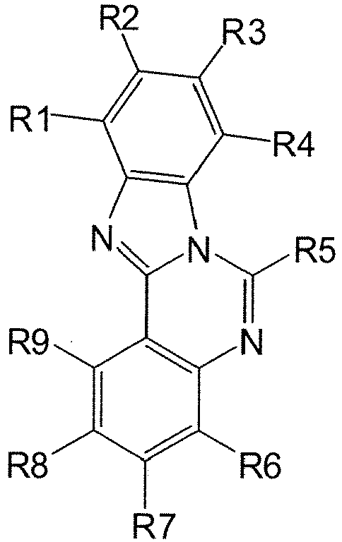
at least one of R1 to R9 is represented by the following Formula 8, and the others are hydrogen; heavy hydrogen; a halogen group; a nitrile group; a nitro group; a hydroxy group; a substituted or unsubstituted cycloalkyl group; a substituted or unsubstituted alkoxy group; a substituted or unsubstituted aryloxy group; a substituted or unsubstituted alkylthioxy group; a substituted or unsubstituted arylthioxy group; a substituted or unsubstituted alkylsulfoxy group; a substituted or unsubstituted arylsulfoxy group; a substituted or unsubstituted alkenyl group; a substituted or unsubstituted silyl group; a substituted or unsubstituted boron group; a substituted or unsubstituted alkylamine group; a substituted or unsubstituted aralkylamine group; a substituted or unsubstituted arylamine group; a substituted or unsubstituted heteroarylamine group; a substituted or unsubstituted aryl group; a substituted or unsubstituted fluorenyl group; a substituted or unsubstituted carbazole group; or a substituted or unsubstituted heterocycle group comprising one or more of N, O and S atoms,
L is a direct bond; a substituted or unsubstituted arylene group; or a substituted or unsubstituted heteroarylene group comprising one or more ofN, O and S atoms,
Ar1 and Ar2 are each independently a substituted or unsubstituted aryl group; or a substituted or unsubstituted heterocycle group comprising one or more of N, O and S atoms, and
A is O, S, or Se. - Further, in the present invention, the compound comprising the phosphine oxide group (-P=O), the thioxophosphine group (-P=S), or the selenoxophosphine group (-P=Se) may be represented by the following Formula 9.

R1 is a naphthyl group or a biphenyl group, and
at least one of R2 to R10 is represented by the following Formula 10, and the others are hydrogen; heavy hydrogen; a halogen group; a nitrile group; a nitro group; a hydroxy group; a substituted or unsubstituted cycloalkyl group; a substituted or unsubstituted alkoxy group; a substituted or unsubstituted aryloxy group; a substituted or unsubstituted alkylthioxy group; a substituted or unsubstituted arylthioxy group; a substituted or unsubstituted alkylsulfoxy group; a substituted or unsubstituted arylsulfoxy group; a substituted or unsubstituted alkenyl group; a substituted or unsubstituted silyl group; a substituted or unsubstituted boron group; a substituted or unsubstituted alkylamine group; a substituted or unsubstituted aralkylamine group; a substituted or unsubstituted arylamine group; a substituted or unsubstituted heteroarylamine group; a substituted or unsubstituted aryl group; a substituted or unsubstituted fluorenyl group; a substituted or unsubstituted carbazole group; or a substituted or unsubstituted heterocycle group comprising one or more of N, O and S atoms,
L is a direct bond; a substituted or unsubstituted arylene group; or a substituted or unsubstituted heteroarylene group comprising one or more of N, O and S atoms,
Ar1 and Ar2 are each independently a substituted or unsubstituted aryl group; or a substituted or unsubstituted heterocycle group comprising one or more of N, O and S atoms, and
A is O, S, or Se. - In the compound according to the present invention, substituent groups of Formulas 1 to 10 will be described in more detail below.
- The alkyl group may be a straight or branched chain, and the number of carbon atoms is not particularly limited but is preferably 1 to 12. Specific examples thereof comprise a methyl group, an ethyl group, a propyl group, an isopropyl group, a butyl group, a t-butyl group, a pentyl group, a hexyl group, a heptyl group and the like, but are not limited thereto.
- The alkenyl group may be a straight or branched chain, and the number of carbon atoms is not particularly limited but is preferably 2 to 12. Specific examples thereof comprise an alkenyl group connected to an aryl group such as a stylbenyl group and a styrenyl group, but are not limited thereto.
- The alkynyl group may be a straight or branched chain, and the number of carbon atoms is not particularly limited but is preferably 2 to 12. Specific examples thereof comprise an ethinyl group, a propynyl group and the like, but are not limited thereto.
- It is preferable that the cycloalkyl group have the 3 to 12 carbon atoms and do not provide steric hindrance. Specific examples thereof comprise a cyclopentyl group, a cyclohexyl group and the like, but are not limited thereto.
- It is preferable that the cycloalkenyl group have 3 to 12 carbon atoms, and more specific examples thereof may comprise a cycle compound having ethenylene in a pentagonal or hexagonal cycle thereof, but are not limited thereto.
- It is preferable that the alkoxy group have 1 to 12 carbon atoms, and more specific examples thereof may comprise methoxy, ethoxy, isopropyloxy and the like, but are not limited thereto.
- It is preferable that the aryloxy group have 6 to 20 carbon atoms, and more specific examples thereof may comprise phenyloxy, cyclohexyloxy, naphthyloxy, diphenyloxy and the like, but are not limited thereto.
- It is preferable that the alkylamine group have 1 to 30 carbon atoms, and more specific examples thereof may comprise a methylamine group, a dimethylamine group, an ethylamine group, a diethylamine group and the like, but are not limited thereto.
- It is preferable that the arylamine group have 5 to 30 carbon atoms, and more specific examples thereof comprise a phenylamine group, a naphthylamine group, a biphenylamine group, an anthracenylamine group, a 3-methyl-phenylamine group, a 4-methyl-naphthylamine group, a 2-methyl-biphenylamine group, a 9-methyl-anthracenylamine group, a diphenylamine group, a phenylnaphthyl amine group, a ditolylamine group, a phenyltolylamine group, a triphenylamine group and the like, but are not limited thereto.
- The aryl group may be a monocycle or a polycycle, and the number of carbon atoms is not particularly limited but is preferably 6 to 40. Examples of the monocyclic aryl group may comprise a phenyl group, a biphenyl group, a terphenyl group, stilben and the like, and examples of the polycyclic aryl group may comprise a naphthyl group, an anthracenyl group, a phenanthrene group, a pyrenyl group, a perylenyl group, a chrysenyl group and the like, but are not limited thereto.
- The heteroaryl group is a heteroatom, a cyclic group comprising O, N, S or P, and the number of carbon atoms is not particularly limited, but is preferably 3 to 30. Examples of the heterocyclic group comprise a carbazole group, a thiophene group, a furan group, a pyrrole group, an imidazole group, a thiazole group, an oxazole group, an oxadiazole group, a triazole group, a pyridyl group, a pyradazine group, a quinolynyl group, an isoquinolynyl group, an acrydyl group and the like, and the compounds of the following Structural Formulas are preferable but are not limited thereto.


- Examples of the halogen group may comprise fluorine, chlorine, bromine, iodine and the like, but are not limited thereto.
- Specific examples of the arylene group may comprise a phenylene group, a biphenylene group, a naphthalenyl group, a binaphthalene group, an anthracenylene group, a fluorenylene group, a chrysenylene group, a phenanthrenylene group and the like, but are not limited thereto.
- Examples of the heterocycloalkyl group may comprise a cyclic group comprising a heteroatom such as N, S or O.
- Further, in the present specification, the term "substituted or unsubstituted" means that substitution is performed by one or more substituent groups selected from the group consisting of heavy hydrogen, a halogen group, an alkyl group, an alkenyl group, an alkoxy group, a silyl group, an arylalkenyl group, an aryl group, a heteroaryl group, a carbazole group, an arylamine group, and a fluorenyl group and a nitrile group substituted or unsubstituted by an aryl group, or there is no substituent group.
- The substituents of Formulas 1 to 10 may be further substituted by an additional substituent group, and examples thereof may comprise a halogen group, an alkyl group, an alkenyl group, an alkoxy group, a silyl group, an arylalkenyl group, an aryl group, a heteroaryl group, a carbazole group, an arylamine group, a fluorenyl group substituted or unsubstituted by an aryl group, a nitrile group and the like, but are not limited thereto.
- Preferable specific examples of the compound represented by Formula 1 comprise the following compounds, but are not limited thereto.








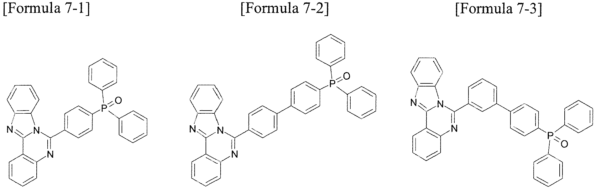
- Preferable specific examples of the compound represented by Formula 7 comprise the following compounds, but are not limited thereto.


- Preferable specific examples of the compound represented by Formula 9 comprise the following compounds, but are not limited thereto.


- Hereinafter, a method of manufacturing the compound represented by Formulas 1 to 10 will be described.
- The compounds represented by Formulas 1 to 10 may be manufactured by using a general method known in the art, such as a condensation reaction and a Suzuki coupling reaction.
- The compounds represented by Formulas 1 to 10 may have properties suitable to be used as the organic material layer used in the organic light emitting device by introducing various substituents into a core structure represented by the aforementioned Formulas. The compounds represented by Formulas 1 to 10 may exhibit properties even though the compounds are used in any layer of the organic light emitting device, but particularly may have the following properties.
- The compounds into which the substituted or unsubstituted arylamine group is introduced are suitable for materials of a light emitting layer and a hole injection and hole transport layer, and the compounds into which the heterocyclic group comprising N is introduced are suitable for materials of an electron injection and electron transport layer and a hole blocking layer.
- The conjugation length of the compound has a close relationship with an energy band gap. Specifically, the energy band gap is reduced as the conjugation length of the compound increases. As described above, since the core of the compounds represented by Formulas 1 to 10 comprises a limited conjugation, the core has properties of from a small energy band gap to a large energy band gap.
- In addition, compounds having intrinsic properties of the introduced substituent groups may be synthesized by introducing various substituent groups to the aforementioned core structure. For example, the material of the hole injection layer and the material of the hole transport layer used when the organic light emitting device is manufactured may be a compound having the energy level that can transporting holes according to HOMO and can prevent electrons from moving from the light emitting layer according to LUMO. In particular, the core structure of the present compound may exhibit a stable property to the electrons, thus contributing to improving a life-span of the device. The derivatives constituted by introducing substituents so as to be used in the materials of the light emitting layer and the electron transport layer may be manufactured so that various arylamine-based dopants, aryl-based dopants, and dopants comprising metal have an appropriate energy band gap.
- Further, the energy band gap can be finely controlled, a property at an interface between organic materials can be improved, and the purpose of the material can become various by introducing various substituent groups to the core structure.
- Meanwhile, since the compounds represented by Formulas 1 to 10 have a high glass transition temperature (Tg), thermal stability is excellent. Such increase in thermal stability is an important factor providing driving stability to the device.
- In the present invention, specific examples of the alkali metal complex may comprise the compound represented by the following Formula 11, but are not limited thereto.

Z and a dashed arc mean two or three atoms and bonds essentially required to perfect a 5- or 6-membered cycle together with M;
A each represent H or a substituent, B each represent a independently selected substituent on a Z atom, with a proviso that two or more substituents may be bonded to each other to form a fused cycle or a fused cycle system;
j is 0 to 3, k is 1 or 2;
M represents alkali metal or alkali earth metal; and
m and n are an integer independently selected so as to provide a neutral charge on a complex. - Formula 11 may be represented by the following Formula 11-a, but is not limited thereto.


- In Formula 11-a, M represents the aforementioned alkali metal or alkali earth metal. M may be Li+, but is not limited thereto. ra and rb may be an each independently selected substituent, but two substituents may be bonded to each other to form a fused cycle group. Examples of the substituent comprise a methyl group, a phenyl group, a fluoro substituent, and a fused benzene cycle group formed by bonding two substituents. In Formula 11-a, t is 1 to 3, s is 1 to 3, and n is an integer of 1 to 6.
- Formula 11 may be represented by the following Formula 11-b, but is not limited thereto.

Y1, Y2, and Y3 each independently represent the substituent, but predetermined Y1, Y2, and Y3 may be bonded to each other to form a cycle or a fused cycle system. M is alkali metal or alkali earth metal, and m and n are integers selected so as to provide neutral charges on a complex. M may be Li+, but is not limited thereto. In the case where the substituent is hydrogen and M represents Li+, Formula 11-b represents lithium acetylacetonate. In addition to hydrogen, examples of other substituents comprise an alkyl group such as a carbocyclic group, a heterocyclic group, and a methyl group, an aryl group such as a phenyl group, or a naphthyl group. The fused cycle group may be formed by bonding two substituents. - Formula 11 may be represented by any one of the following Formulas 11-1 to 11-30, but is not limited thereto.


[Formula 11-25] [Formula 11-26] [Formula 11-27] Li2O LiF CsF

- In the present invention, one or more layers of the organic material layer comprise a compound where the alkali metal complex like Formula 11 is docked to one or more of a hetero atom, the phosphine oxide group, the thioxophosphine group, and the selenoxophosphine group of one or more compounds of a heteroaryl-based compound; and a compound comprising the phosphine oxide group (-P=O), the thioxophosphine group (-P=S), or the selenoxophosphine group (-P=Se).
- More specifically, the metal atom of the alkali metal complex may be docked to the hetero atom of the heteroaryl-based compound. Further, the metal atom of the alkali metal complex may be docked to O, S, or Se of one or more compounds of the compounds comprising the phosphine oxide group (-P=O), the thioxophosphine group (-P=S), or the selenoxophosphine group (-P=Se).
- Further, the compound comprising the phosphine oxide group (-P=O), the thioxophosphine group (-P=S), or the selenoxophosphine group (-P=Se) may be a heteroaryl-based compound further comprising a hetero atom such as a nitrogen (N) atom. In this case, the metal atom of the alkali metal complex may be further docked to O, S, or Se and N.
- That is, in the present invention, when the organic material layer of the organic light emitting device is formed, in the case where one or more compounds of the heteroaryl-based compound; and the compound comprising the phosphine oxide group (-P=O), the thioxophosphine group (-P=S), or the selenoxophosphine group (-P=Se) are codeposited together with the alkali metal complex, the hetero atom, the phosphine oxide group (-P=O), the thioxophosphine group (-P=S), or the selenoxophosphine group (-P=Se) of one or more compounds of the heteroaryl-based compound; and the compound comprising the phosphine oxide group (-P=O), the thioxophosphine group (-P=S), or the selenoxophosphine group (-P=Se) plays a role of a docking site with the alkali metal complex, such that the dipole moment of the compound comprised in the organic material layer is increased, thus increasing a life-span property of the organic light emitting device.
- In the present invention, the term "docking" means a state where one or more of the hetero atom, the phosphine oxide group, the thioxophosphine group, and the selenoxophosphine group of one or more compounds of the heteroaryl-based compound; and the compound comprising the phosphine oxide group (-P=O), the thioxophosphine group (-P=S), or the selenoxophosphine group (-P=Se), and the alkali metal complex are bonded to each other by a London dispersion force or a dipole-induced dipole force.
- In the present invention, the dipole moment of the docked compound may be calculated by the following Equation.
-

- ■ ρ (r0): molecular density
- ■ V: volume
- ■ r : the point of observation
- ■ d3r0 : an elementary volume
- In the above, a molecular density is obtained by calculation to obtain the aforementioned dipole value, the charge and the dipole for each atom are obtained from the molecular density by using a method of Hirshfeld charge analysis, and the dipole moment may be calculated by putting the calculated result into the aforementioned Equation according to the following Equation.
-

■ ρ (r) : molecular density
■ ρα (r - R α ): density of the free atom α located at coordinates Rα➢Atomic Charge ➢Weight Function 

■ W (r) : weight function - In the present invention, the compound where the alkali metal complex is docked to one or more compounds of the heteroaryl-based compound; and the compound comprising the phosphine oxide group (-P=O), the thioxophosphine group (-P=S), or the selenoxophosphine group (-P=Se) may be used to change the dipole moment of the compound as compared to the compound where the alkali metal complex is not docked. Therefore, a life-span of the organic light emitting device may be more effectively increased.
- In the present invention, the organic material layer may have a multilayered structure comprising a hole injection layer, a hole transport layer, a light emitting layer, an electron transport layer and the like, but is not limited thereto and may have a single layer structure. Further, the organic material layer may be manufactured to have the smaller number of layers by using various polymer materials and by not a deposition method but a solvent process, for example, a method such as spin coating, dip coating, doctor blading, screen printing, inkjet printing, or a heat transferring method.
- Particularly, in the present invention, it is more preferable that the compound where the dipole moment is changed be comprised in the electron transport layer.
- Further, the method of manufacturing the organic light emitting device according to the present invention comprises sequentially forming a first electrode, an organic material layer, and a second electrode on a substrate, and forming at least one layer of organic material layers by codepositing one or more compounds of compounds comprising the heteroaryl-based compound, and the phosphine oxide-based compound, or the compound comprising the heteroaryl group and the phosphine oxide group together with an alkali metal complex.
- A weight ratio of the alkali metal complex to the heteroaryl-based compound, the phosphine oxide-based compound, or the compound comprising the heteroaryl group and the phosphine oxide group may be 0.1 to 0.7, or 0.1 to 0.5, but is not limited thereto.
- The organic light emitting device according to the present invention may be manufactured by using a manufacturing method and a material of a general organic light emitting device, except that one or more organic material layers are formed by using the aforementioned compounds.
- The organic material layer of the organic electronic device of the present invention may be constituted by a single layer structure, but by a multilayered structure in which two or more organic material layers are laminated. For example, the organic electronic device of the present invention may have a structure comprising a hole injection layer, a hole transport layer, a light emitting layer, an electron transport layer, an electron injection layer and the like as an organic material layer. However, the structure of the organic electronic device is not limited thereto, but may comprise the smaller number of organic material layers.
- Accordingly, in the organic electronic device of the present invention, the organic material layer may comprise one or more layers of the hole injection layer, the hole transport layer, and a layer injecting and transporting holes simultaneously, and one or more layers of the layers may comprise the compound according to the present invention.
- Further, the organic material layer may comprise the light emitting layer, and the light emitting layer may comprise the compound according to the present invention.
- Further, the organic material layer may comprise one or more layers of an electron transport layer, an electron injection layer, and a layer transporting and injecting electrons simultaneously, and one or more layers of the layers may comprise the compound according to the present invention.
- In the organic material layer having the multilayered structure, the compound according to the present invention may be comprised in a light emitting layer, a layer injecting/transporting holes and emitting light simultaneously, a layer transporting holes and emitting light simultaneously, a layer transporting electrons and emitting light simultaneously or the like.
- For example, the structure of the organic light emitting device of the present invention may have a structure shown in
FIGS. 1 to 4 , but is not limited thereto. -
FIG. 1 shows a structure of an organic light emitting device, in which ananode 102, alight emitting layer 105, and acathode 107 are sequentially laminated on asubstrate 101. In the aforementioned structure, the compound according to the present invention may be comprised in thelight emitting layer 105. -
FIG. 2 shows an example of a structure of an organic light emitting device, in which ananode 102, hole injection/hole transport and light emittinglayers 105, anelectron transport layer 106, and acathode 107 are sequentially laminated on asubstrate 101. In the aforementioned structure, the compound according to the present invention may be comprised in the hole injection/hole transport and light emitting layers 105. -
FIG. 3 shows an example of a structure of an organic light emitting device, in which asubstrate 101, ananode 102, a hole injection layer 103, hole transport and light emittinglayers 105, anelectron transport layer 106, and acathode 107 are sequentially laminated. In the aforementioned structure, the compound according to the present invention may be comprised in the hole injection/hole transport and light emitting layers 105. -
FIG. 4 shows an example of a structure of an organic light emitting device, in which asubstrate 101, ananode 102, a hole injection layer 103, a hole transport layer 104, electron transport and light emittinglayers 105, and acathode 107 are sequentially laminated. In the aforementioned structure, the compound according to the present invention may be comprised in the electron transport and light emitting layers 105. - For example, the organic light emitting device according to the present invention may be manufactured by forming the anode by depositing metal or metal oxides having the conductivity or an alloy thereof on the substrate by using a PVD (physical vapor deposition) method such as sputtering or e-beam evaporation, forming the organic material layer comprising the hole injection layer, the hole transport layer, the light emitting layer, and the electron transport layer thereon, and depositing the material that is capable of being used as the cathode thereon. In addition to this method, the organic light emitting device may be manufactured by sequentially depositing a cathode material, an organic material layer, and an anode material on the substrate.
- The organic material layer may have a multilayered structure comprising the hole injection layer, the hole transport layer, the light emitting layer, the electron transport layer and the like, but is not limited thereto and may have a single layer structure. Further, the organic material layer may be manufactured to have the smaller number of layers by using various polymer materials and by not the deposition method but the solvent process, for example, a method such as spin coating, dip coating, doctor blading, screen printing, inkjet printing, or the heat transferring method.
- It is preferable that the anode material be, in general, a material having a large work function so as to smoothly perform hole injection into the organic material layer. Specific examples of the anode material that is capable of being used in the present invention comprise metal such as vanadium, chrome, copper, zinc and gold, or an alloy thereof; metal oxides such as zinc oxides, indium oxides, indium tin oxides (ITO) and indium zinc oxides (IZO); a combination of metal and oxides such as ZnO:Al or SnO2:Sb; conductive polymers such as poly(3-methyl compound), poly[3,4-(ethylene-1,2-dioxy) compound](PEDT), polypyrole, and polyaniline and the like, but are not limited thereto.
- It is preferable that the cathode material be, in general, a material having a small work function so as to smoothly perform electron injection into the organic material layer. Specific examples of the cathode material comprise metal such as magnesium, calcium, sodium, potassium, titanium, indium, yttrium, lithium, gadolinium, aluminum, silver, tin, and lead, or an alloy thereof; a multilayered structure material such as LiF/Al or LiO2/Al, and the like but are not limited thereto.
- The hole injection material is a material that is capable of well receiving holes from the anode at a low voltage, and it is preferable that the HOMO (highest occupied molecular orbital) of the hole injection material be a value between the work function of the anode material and the HOMO of the organic material layer therearound. Specific examples of the hole injection material comprise metal porphyrine, oligothiophene, an arylamine-based organic material, a hexanitrilehexaazatriphenylene-based organic material, a quinacridone-based organic material, a perylene-based organic material, anthraquinone, polyaniline, a polycompound-based conductive polymer and the like, but are not limited thereto.
- The hole transport material is a material that is capable of receiving the holes from the anode or the hole injection layer and transporting the holes to the light emitting layer, and is preferably a material having large mobility to the holes. Specific examples thereof comprise an arylamine-based organic material, a conductive polymer, a block copolymer in which a conjugate portion and a non-conjugate portion are present together, and the like, but are not limited thereto.
- The light emitting material is a material that is capable of receiving the holes and the electrons from the hole transport layer and the electron transport layer and bonds the holes and the electrons to emit light in a visible ray region, and is preferably a material having excellent photon efficiency to fluorescence or phosphorescence. Specific examples thereof comprise a 8-hydroxy-quinoline aluminum complex (Alq3); a carbazole-based compound; a dimerized styryl compound; BAlq; a 10-hydroxybenzoquinoline-metal compound; a benzoxazole, benzthiazole and benzimidazole-based compound; a poly(p-phenylenevinylene) (PPV)-based polymer; a spiro compound; polyfluorene, lubrene, and the like, but are not limited thereto.
- The electron transport material is a material that is capable of receiving the electrons well from the cathode and transporting the electrons to the light emitting layer, and is preferably a material having large mobility to the electrons. Specific examples thereof comprise a 8-hydroxyquinoline Al complex; a complex comprising Alq3; an organic radical compound; a hydroxyflavone metal complex, and the like, but are not limited thereto.
- The organic light emitting device according to the present invention may be a top emission type, a bottom emission type, or a both-sided emission type according to the used material.
- The compound according to the present invention may be applied to an organic electronic device such as an organic solar cell, an organic photoconductor, and an organic transistor by the principle that is similar to the principle applied to the organic light emitting device.
- Hereinafter, preferable Examples will be described in order to help understanding of the present invention. However, the following Examples are set forth to illustrate the present invention, but the scope of the present invention is not limited thereto.
- The compound represented by the following
Formula 12 was used to measure a change in dipole moment according to bonding of the additional substituent group to the compound represented by the followingFormula 12, and the result is described in the following Table 1.


- The compound represented by
Formula 13 is a compound where the phosphine oxide group is further bonded to the compound represented byFormula 12, and the compound represented by Formula 14 is a compound where the alkali metal complex is docked to the nitrogen atom of the compound represented byFormula 13. Further, the compound represented by Formula 15 is a compound where the alkali metal complex is docked to the phosphine oxide group of the compound represented byFormula 13, and the compound represented by Formula 16 is a compound where the alkali metal complex is docked to both the nitrogen atom and the phosphine oxide group of the compound represented byFormula 13. - In Formulas 14 to 16, LiQ is a compound represented by the following Formula 11-1.

[Table 1] Compound Dipole moment Formula 12 3.07 Formula 136.51 Formula 14 10.80 Formula 15 12.49 Formula 16 15.85 - As described above, it can be seen that as compared to the compound where the alkali metal complex is not docked, the dipole moment of the compound where the alkali metal complex is docked to the hetero atom and/or the phosphine oxide group of the compound is increased.
- In the case where the dipole moment of the compound comprised in the electron transport layer of the organic light emitting device is large, arrangment of molecules becomes irregular to densify the layer, accordingly, the organic light emitting device can endure stress well to improve a life-span property.
- In the present invention, since there is a limit in increase of the dipole moment only by the molecule, as described above, the dipole moment may be more increased by using the layer where the heteroaryl-based compound, the phosphine oxide-based compound, or the compound comprising the heteroaryl group and the phosphine oxide group and the alkali metal complex are mixed as the electron transport layer, thus improving a life-span property of the organic light emitting device.
- The life-span properties of the organic light emitting device where only the compound represented by
Formula 12 is applied to the electron transport layer and the organic light emitting device where the compound represented byFormula 12 and the alkali metal complex (LiQ) are applied together to the electron transport layer were evaluated, and the result is described in the followingFIG. 5 . Herein, other constitution components of the organic light emitting device were the same, except that the compound constituting the electron transport layer was changed. - As shown in the following
FIG. 5 , it can be seen that the life-span property of the organic light emitting device of the present invention, in which the dipole moment of the compound comprised in the organic material layer is increased, is improved by two times as compared to the organic light emitting device in which the dipole moment thereof is not increased. - The life-span properties of the organic light emitting device where only the compound represented by
Formula 13 is applied to the electron transport layer and the organic light emitting device where the compound represented byFormula 13 and the alkali metal complex (LiQ) are applied together to the electron transport layer were evaluated, and the result is described in the followingFIG. 6 . - As shown in the following
FIG. 6 , it can be seen that the life-span property of the organic light emitting device of the present invention, in which the dipole moment of the compound comprised in the organic material layer is increased, is improved by four times as compared to the organic light emitting device in which the dipole moment thereof is not increased. - As described above, an organic light emitting device according to the present invention comprises a first electrode, a second electrode, and one or more organic material layers disposed between the first electrode and the second electrode, and a life-span property of the organic light emitting device can be largely improved by changing a dipole moment of a compound comprised in the organic material layers.
Claims (19)
- An organic light emitting device comprising:a first electrode,a second electrode, andone or more organic material layers disposed between the first electrode and the second electrode,wherein one or more layers of the organic material layers comprise a compound where an alkali metal complex is docked to one or more of a hetero atom, a phosphine oxide group, a thioxophosphine group, and a selenoxophosphine group of one or more compounds of a heteroaryl-based compound; and a compound comprising the phosphine oxide group (-P=O), the thioxophosphine group (-P=S), or the selenoxophosphine group (-P=Se).
- The organic light emitting device of claim 1, wherein the compound comprising the phosphine oxide group (-P=O), the thioxophosphine group (-P=S), or the selenoxophosphine group (-P=Se) is represented by the following Formula 1:

X1 is N or CR3, X2 is N or CR4, X3 is N or CR5, X4 is N or CR6, Y1 is N or CR7, Y2 is N or CR8, Y3 is N or CR9, Y4 is N or CR10, all of X1 to X4 and Y1 to Y4 are not N, R3 to R10 are each independently -(L)p-(Y)q or represented by the following Formula 1A, at least one of R3 to R10 is represented by the following Formula 1A, p is an integer of 0 to 10, q is an integer of 1 to 10, and two or more adjacent groups of R3 to R10 may form a monocycle or polycycle,
Y is hydrogen; heavy hydrogen; a halogen group; a nitrile group; a nitro group; a hydroxy group; a substituted or unsubstituted cycloalkyl group; a substituted or unsubstituted alkoxy group; a substituted or unsubstituted aryloxy group; a substituted or unsubstituted alkylthioxy group; a substituted or unsubstituted arylthioxy group; a substituted or unsubstituted alkylsulfoxy group; a substituted or unsubstituted arylsulfoxy group; a substituted or unsubstituted alkenyl group; a substituted or unsubstituted silyl group; a substituted or unsubstituted boron group; a substituted or unsubstituted alkylamine group; a substituted or unsubstituted aralkylamine group; a substituted or unsubstituted arylamine group; a substituted or unsubstituted heteroarylamine group; a substituted or unsubstituted aryl group; a substituted or unsubstituted fluorenyl group; a substituted or unsubstituted carbazole group; or a substituted or unsubstituted heterocycle group comprising one or more of N, O and S atoms,
R1 and R2 may be connected to each other to form or not to form a substituted or unsubstituted aliphatic, aromatic or heteroaromatic monocycle or polycycle, and in the case where R1 and R2 does not form the cycle, R1 and R2 are the same as or different from each other and each independently hydrogen, a substituted or unsubstituted C3∼C40 cycloalkyl group; a substituted or unsubstituted C6 ∼ C60 aryl group; a substituted or unsubstituted C2 ∼ C40 alkenyl group; or a substituted or unsubstituted C2 ∼ C60 heterocycle group,
the aromatic or heteroaromatic monocycle and polycycle formed by connecting R1, R2, and R1 and R2 to each other may be each independently substituted by -(L)p-(Y)q,
in the case where two or more L and two or more Y are present, L and Y are each independently the same as or different from each other,
A are each independently O, S or Se,
Ar1 and Ar2 are each independently a substituted or unsubstituted aryl group; or a substituted or unsubstituted heterocycle group comprising one or more of N, O and S atoms,
Ar3 are each independently a substituted or unsubstituted arylene group; or a substituted or unsubstituted heteroarylene group comprising one or more of N, O and S atoms. - The organic light emitting device of claim 2, wherein the Formula 1 is represented by the following Formula 2:

X1 to X4, and Y1 to Y4 are the same as definitions of the Formula 1,
N of (N)n1 means a nitrogen atom and also that the nitrogen atom may replace a carbon atom in a benzene cycle,
n1 of (N)n1 is an integer of 0 to 6,
R11 is the same as definition of R3 to R10 of the Formula 1, and
k1 is an integer of 0 to 4. - The organic light emitting device of claim 2, wherein the Formula 1 is represented by the following Formula 3 or 4:


X1 to X4, and Y1 to Y4 are the same as definitions of the Formula 1,
N of (N)n1 and (N)n2 means a nitrogen atom and also that the nitrogen atom may replace a carbon atom in a benzene cycle,
n1 of (N)n1 is an integer of 0 to 2,
n2 of (N)n2 is an integer of 0 to 2,
R11 and R12 are each independently the same as definitions of R3 to R10 of the Formula 1,
k1 is an integer of 0 to 4, and k2 is an integer of 0 to 4. - The organic light emitting device of claim 2, wherein the Formula 1 is represented by the following Formula 5:

X1 to X4, and Y1 to Y4 are the same as definitions of the Formula 1,
N of (N)n1 and (N)n2 means a nitrogen atom and also that the nitrogen atom may replace a carbon atom in a benzene cycle,
n1 of (N)n1 is an integer of 0 to 2,
n2 of (N)n2 is an integer of 0 to 2,
R11 and R12 are each independently the same as definitions of R3 to R10 defined in the Formula 1,
k1 is an integer of 0 to 4, and k2 is an integer of 0 to 4. - The organic light emitting device of claim 2, wherein the Formula 1 is represented by the following Formula 6:
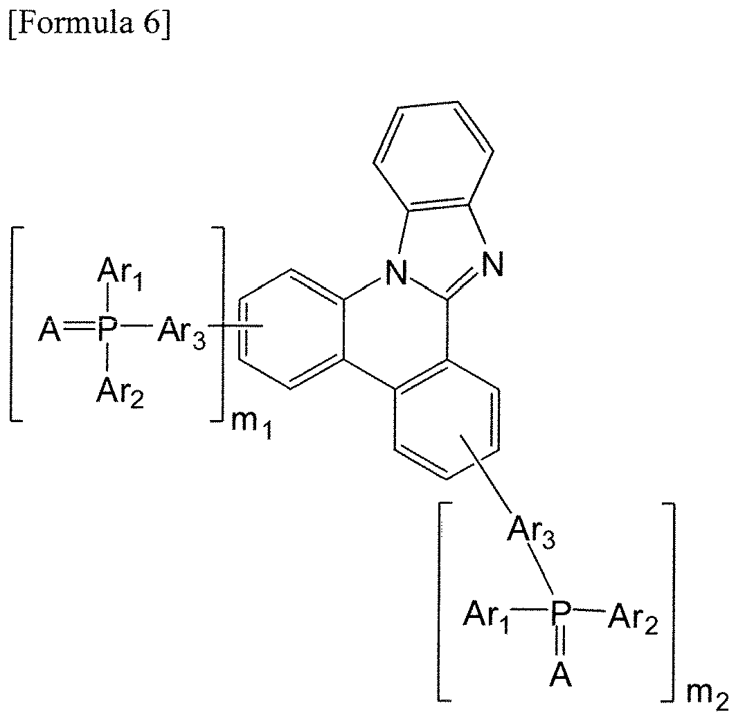
Ar1 to Ar3, and A are the same as definitions of the Formula 1,
m1 is an integer of 0 to 4, and m2 is an integer of 0 to 4, with a proviso that the case where m1 and m2 are both 0 is excluded. - The organic light emitting device of claim 2, wherein the compound represented by the Formula 1 is represented by any one of the following Formulas:



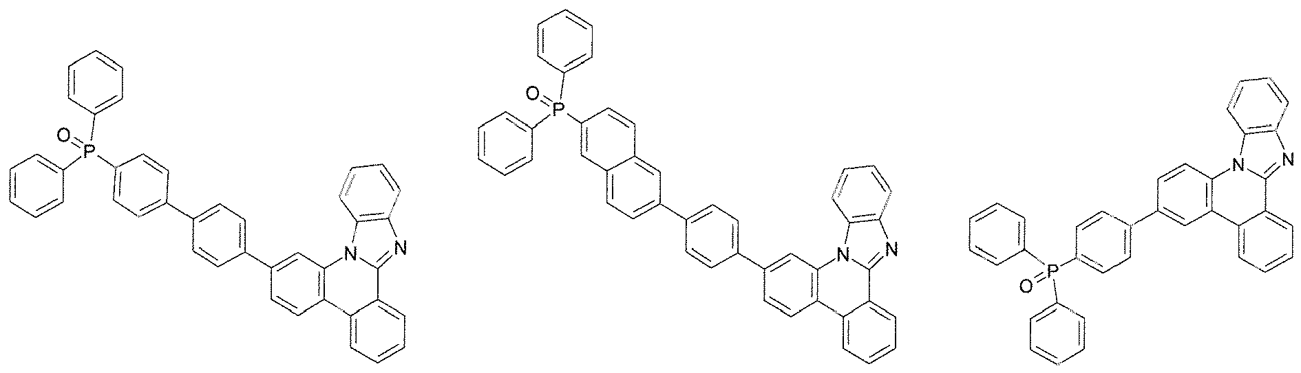


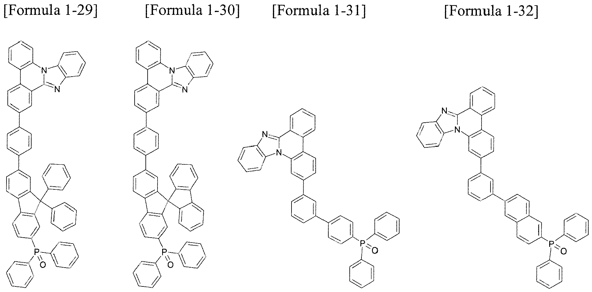


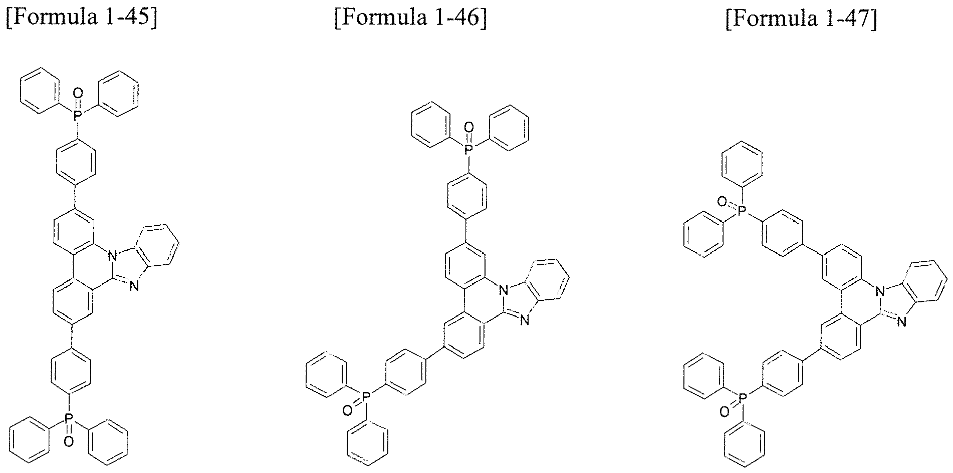


- The organic light emitting device of claim 1, wherein the compound comprising the phosphine oxide group (-P=O), the thioxophosphine group (-P=S), or the selenoxophosphine group (-P=Se) is represented by the following Formula 7:


at least one of R1 to R9 is represented by the following Formula 8, and the others are hydrogen; heavy hydrogen; a halogen group; a nitrile group; a nitro group; a hydroxy group; a substituted or unsubstituted cycloalkyl group; a substituted or unsubstituted alkoxy group; a substituted or unsubstituted aryloxy group; a substituted or unsubstituted alkylthioxy group; a substituted or unsubstituted arylthioxy group; a substituted or unsubstituted alkylsulfoxy group; a substituted or unsubstituted arylsulfoxy group; a substituted or unsubstituted alkenyl group; a substituted or unsubstituted silyl group; a substituted or unsubstituted boron group; a substituted or unsubstituted alkylamine group; a substituted or unsubstituted aralkylamine group; a substituted or unsubstituted arylamine group; a substituted or unsubstituted heteroarylamine group; a substituted or unsubstituted aryl group; a substituted or unsubstituted fluorenyl group; a substituted or unsubstituted carbazole group; or a substituted or unsubstituted heterocycle group comprising one or more of N, O and S atoms,
L is a direct bond; a substituted or unsubstituted arylene group; or a substituted or unsubstituted heteroarylene group comprising one or more ofN, O and S atoms,
Ar1 and Ar2 are each independently a substituted or unsubstituted aryl group; or a substituted or unsubstituted heterocycle group comprising one or more of N, O and S atoms, and
A is O, S, or Se. - The organic light emitting device of claim 8, wherein the compound represented by the Formula 7 is represented by any one of the following Formulas:


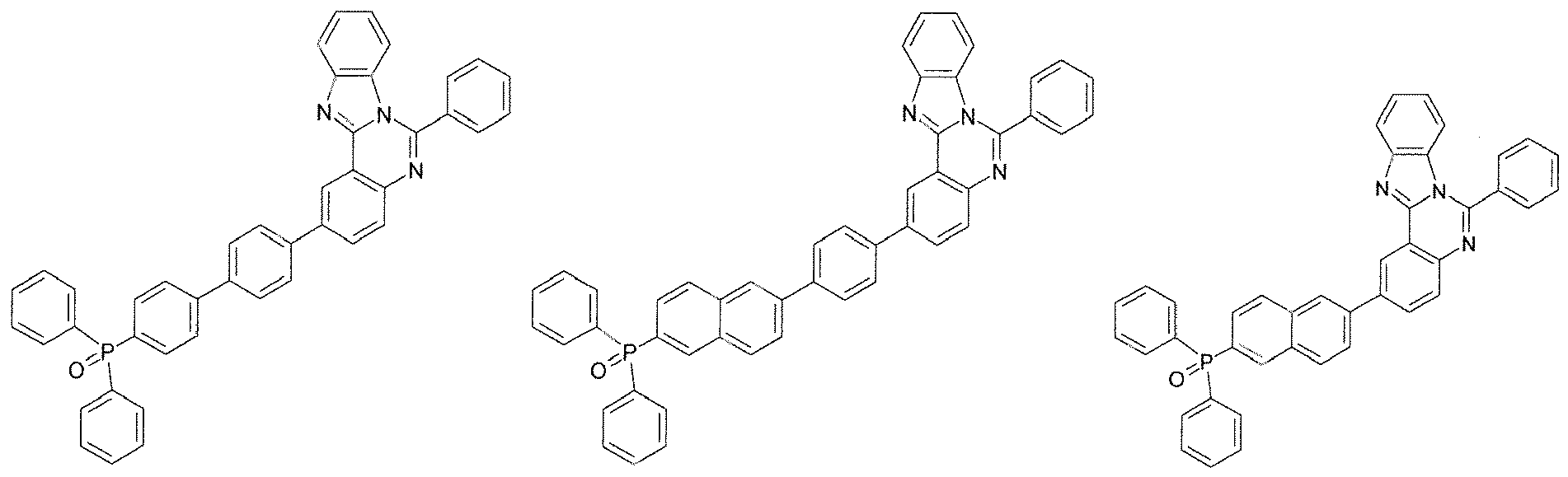

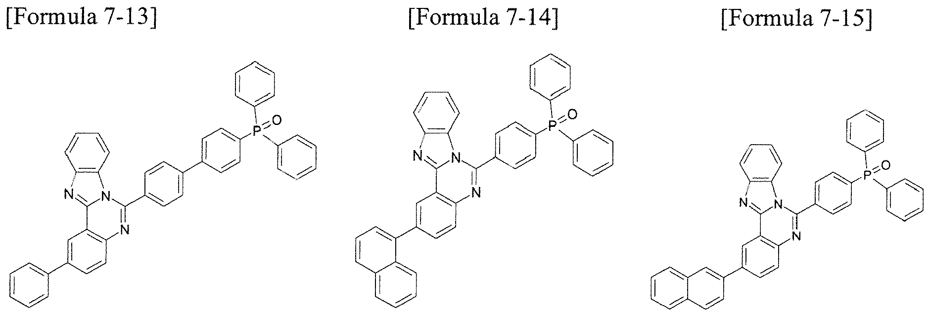


- The organic light emitting device of claim 1, wherein the compound comprising the phosphine oxide group (-P=O), the thioxophosphine group (-P=S), or the selenoxophosphine group (-P=Se) is represented by the following Formula 9:

R1 is a naphthyl group or a biphenyl group, and
at least one of R2 to R10 is represented by the following Formula 10, and the others are hydrogen; heavy hydrogen; a halogen group; a nitrile group; a nitro group; a hydroxy group; a substituted or unsubstituted cycloalkyl group; a substituted or unsubstituted alkoxy group; a substituted or unsubstituted aryloxy group; a substituted or unsubstituted alkylthioxy group; a substituted or unsubstituted arylthioxy group; a substituted or unsubstituted alkylsulfoxy group; a substituted or unsubstituted arylsulfoxy group; a substituted or unsubstituted alkenyl group; a substituted or unsubstituted silyl group; a substituted or unsubstituted boron group; a substituted or unsubstituted alkylamine group; a substituted or unsubstituted aralkylamine group; a substituted or unsubstituted arylamine group; a substituted or unsubstituted heteroarylamine group; a substituted or unsubstituted aryl group; a substituted or unsubstituted fluorenyl group; a substituted or unsubstituted carbazole group; or a substituted or unsubstituted heterocycle group comprising one or more of N, O and S atoms,
L is a direct bond; a substituted or unsubstituted arylene group; or a substituted or unsubstituted heteroarylene group comprising one or more of N, O and S atoms,
Ar1 and Ar2 are each independently a substituted or unsubstituted aryl group; or a substituted or unsubstituted heterocycle group comprising one or more of N, O and S atoms, and
A is O, S, or Se. - The organic light emitting device of claim 10, wherein the compound represented by the Formula 9 is represented by any one of the following Formulas:
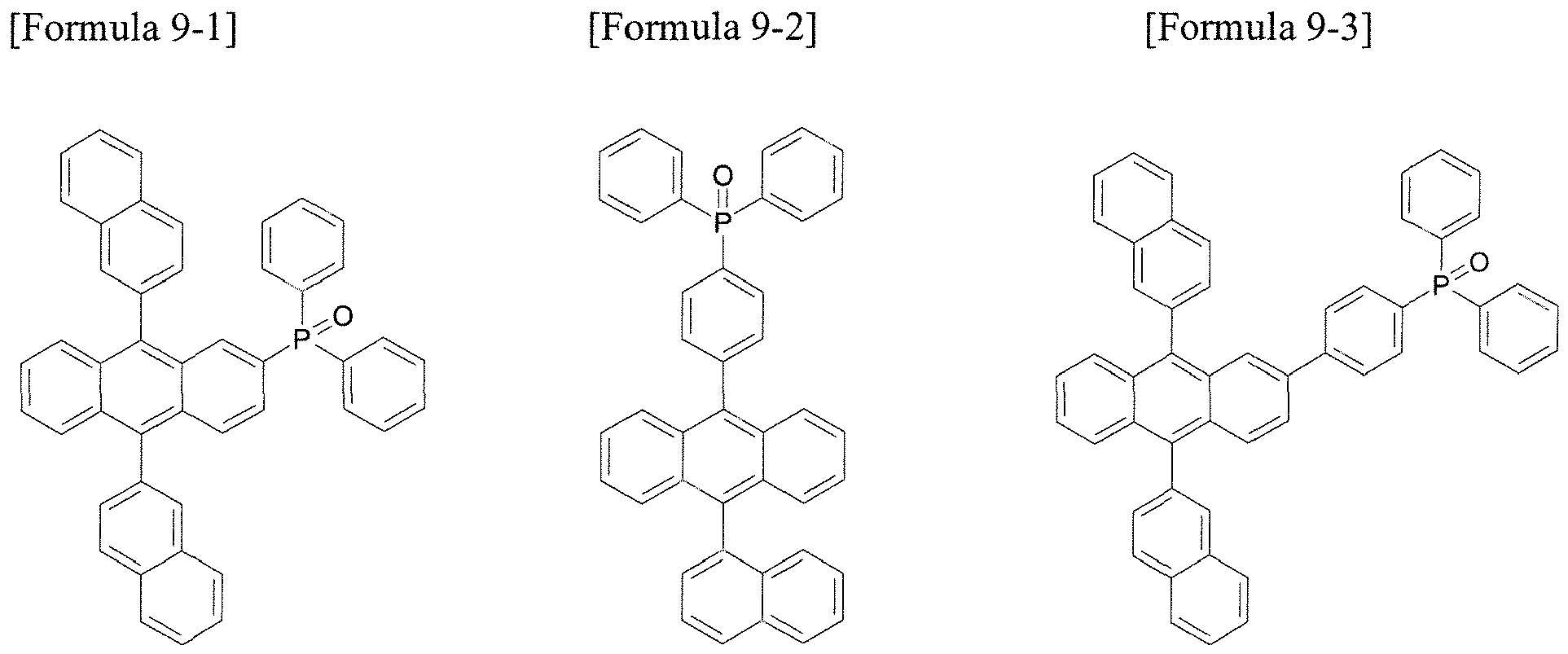
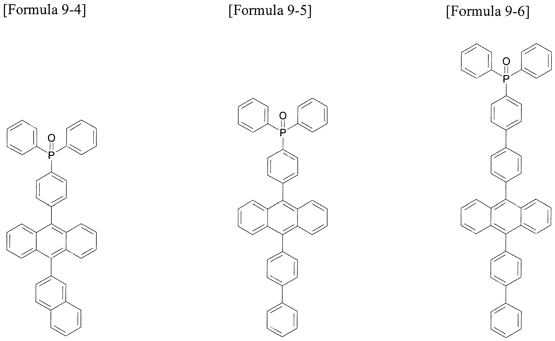


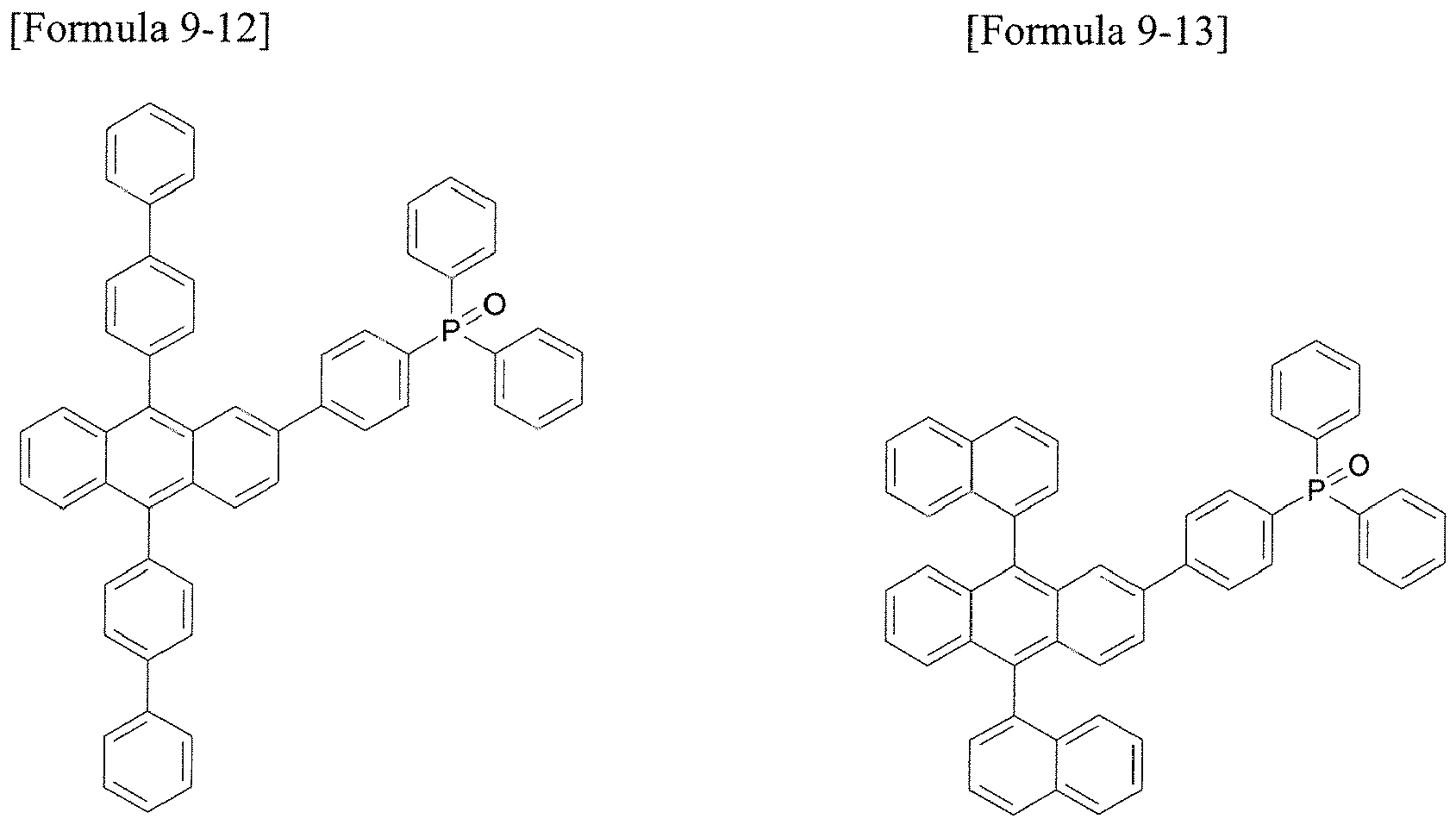
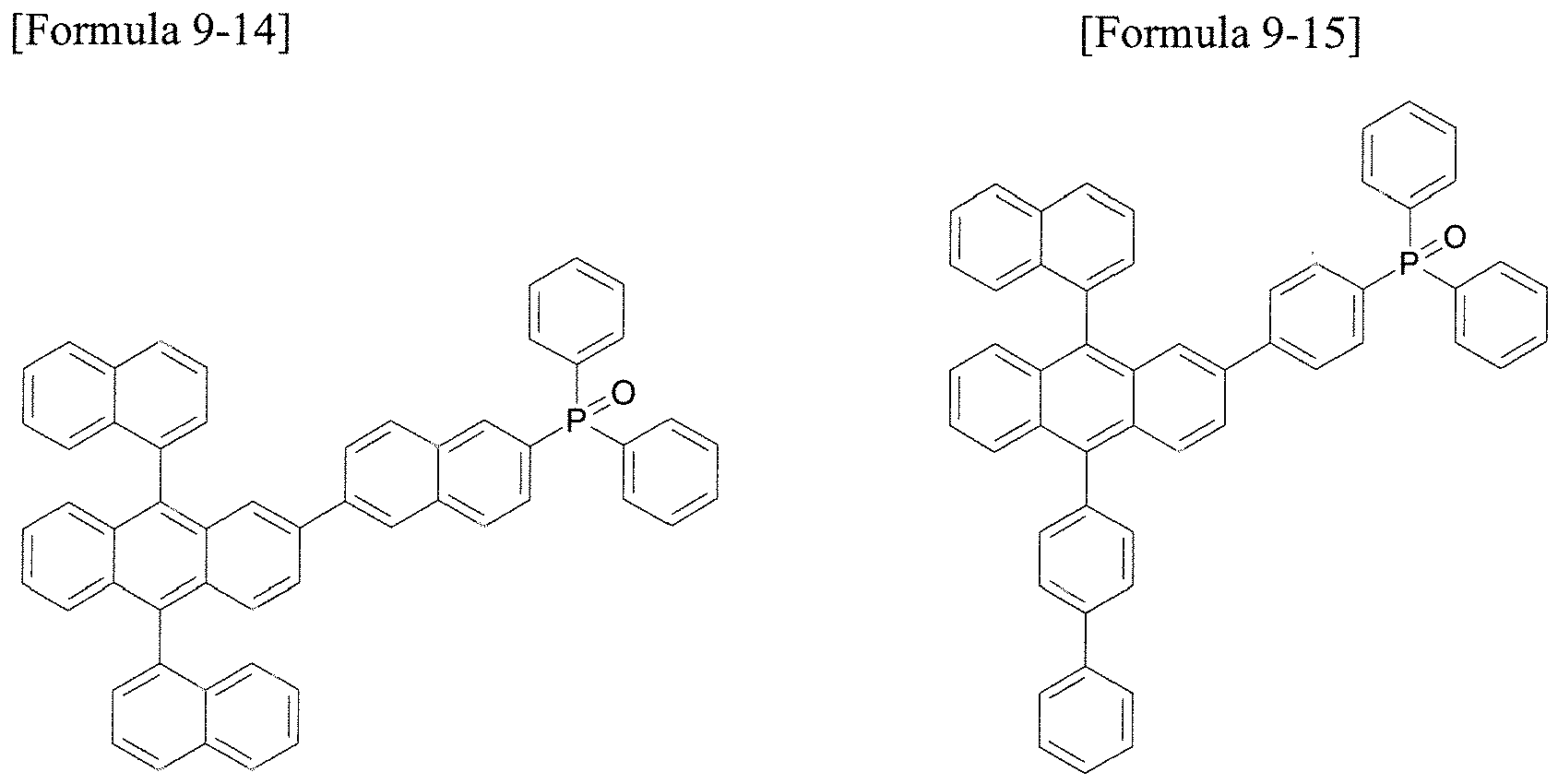
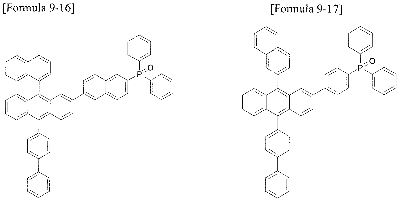


- The organic light emitting device of claim 1, wherein the alkali metal complex is a compound represented by the following Formula 11:

Z and a dashed arc mean two or three atoms and bonds essentially required to perfect a 5- or 6-membered cycle together with M;
A each represent H or a substituent, B each represent a independently selected substituent on a Z atom, with a proviso that two or more substituents may be bonded to each other to form a fused cycle or a fused cycle system;
j is 0 to 3, k is 1 or 2;
M represents alkali metal or alkali earth metal; and
m and n are an integer independently selected so as to provide a neutral charge on a complex. - The organic light emitting device of claim 12, wherein the compound represented by the Formula 11 is represented by any one of the following Formulas:


[Formula 11-25] Li2O
[Formula 11-26] LiF
[Formula 11-27] CsF
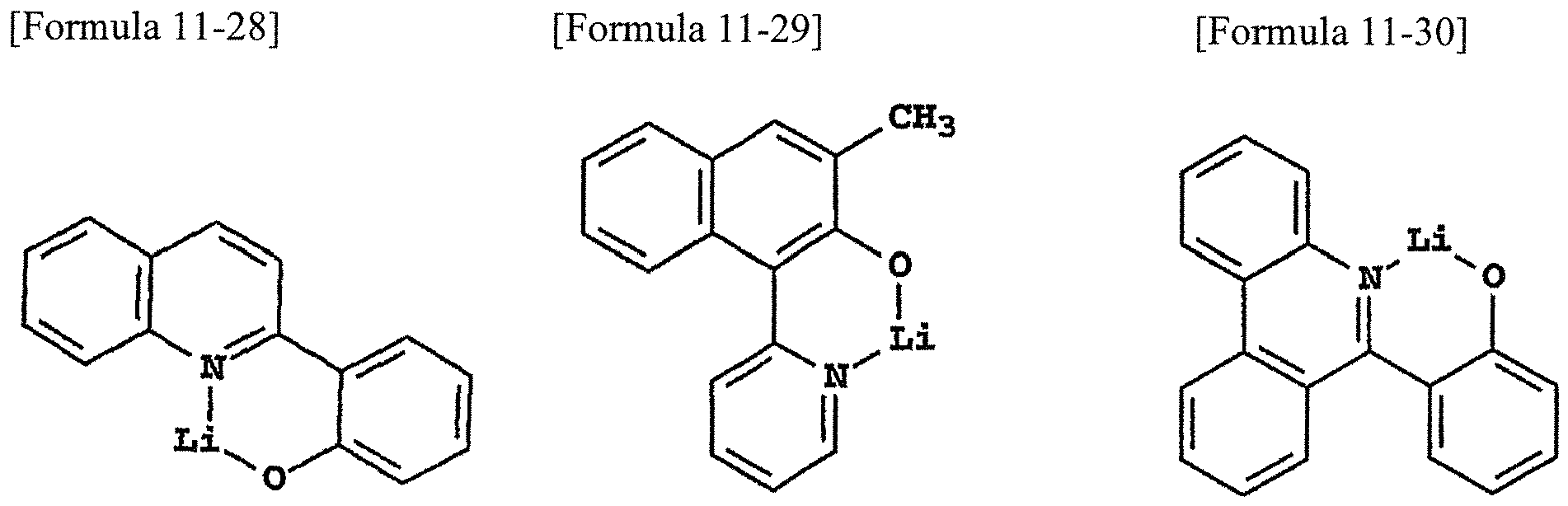
- The organic light emitting device of claim 1, wherein the alkali metal complex is docked to the hetero atom of the heteroaryl-based compound.
- The organic light emitting device of claim 1, wherein the alkali metal complex is docked to O, S, or Se of the compound comprising the phosphine oxide group (-P=O), the thioxophosphine group (-P=S), or the selenoxophosphine group (-P=Se).
- The organic light emitting device of claim 1, wherein the compound comprising the phosphine oxide group (-P=O), the thioxophosphine group (-P=S), or the selenoxophosphine group (-P=Se) is a heteroaryl-based compound further comprising a nitrogen (N) atom, and the alkali metal complex is docked to O, S, or Se and the nitrogen(N) atom together.
- The organic light emitting device of claim 1, wherein the organic material layer comprising the compound where the alkali metal complex is docked to one or more of the hetero atom, the phosphine oxide group, the thioxophosphine group, and the selenoxophosphine group of one or more compounds of the heteroaryl-based compound; and a compound comprising the phosphine oxide group (-P=O), the thioxophosphine group (-P=S), or the selenoxophosphine group (-P=Se) is an electron transport layer.
- A method of manufacturing an organic light emitting device, comprising:sequentially forming a first electrode, an organic material layer, and a second electrode on a substrate, andforming at least one layer of organic material layers by codepositing one or more compounds of compounds comprising a heteroaryl-based compound; and a phosphine oxide group(-P=O), a thioxophosphine group (-P=S), or a selenoxophosphine group (-P=Se) together with an alkali metal complex.
- The method of manufacturing an organic light emitting device of claim 18, wherein a weight ratio of an alkali metal complex to the heteroaryl-based compound, the phosphine oxide-based compound, or the compound comprising a heteroaryl group and the phosphine oxide group is 0.1 to 0.7.
Applications Claiming Priority (2)
| Application Number | Priority Date | Filing Date | Title |
|---|---|---|---|
| KR20110101513 | 2011-10-05 | ||
| PCT/KR2012/008062 WO2013051875A2 (en) | 2011-10-05 | 2012-10-05 | Organic light-emitting device and method for manufacturing same |
Publications (3)
| Publication Number | Publication Date |
|---|---|
| EP2750214A2 true EP2750214A2 (en) | 2014-07-02 |
| EP2750214A4 EP2750214A4 (en) | 2015-07-22 |
| EP2750214B1 EP2750214B1 (en) | 2020-06-17 |
Family
ID=48044304
Family Applications (1)
| Application Number | Title | Priority Date | Filing Date |
|---|---|---|---|
| EP12837913.8A Active EP2750214B1 (en) | 2011-10-05 | 2012-10-05 | Organic light-emitting device and method for manufacturing same |
Country Status (7)
| Country | Link |
|---|---|
| US (1) | US9887368B2 (en) |
| EP (1) | EP2750214B1 (en) |
| JP (1) | JP5933691B2 (en) |
| KR (1) | KR101464408B1 (en) |
| CN (1) | CN103548172B (en) |
| TW (1) | TWI462928B (en) |
| WO (1) | WO2013051875A2 (en) |
Cited By (4)
| Publication number | Priority date | Publication date | Assignee | Title |
|---|---|---|---|---|
| EP3232490A1 (en) * | 2016-04-12 | 2017-10-18 | Novaled GmbH | Organic light emitting diode comprising an organic semiconductor layer |
| EP3406599A1 (en) * | 2017-05-23 | 2018-11-28 | Novaled GmbH | Organic electronic device comprising an organic semiconductor layer |
| EP3417495B1 (en) | 2016-02-19 | 2020-05-27 | Novaled GmbH | Electron transport layer comprising a matrix compound mixture for an organic light-emitting diode (oled) |
| US11005049B2 (en) | 2013-08-20 | 2021-05-11 | Merck Patent Gmbh | Metal complexes |
Families Citing this family (44)
| Publication number | Priority date | Publication date | Assignee | Title |
|---|---|---|---|---|
| EP2719742B1 (en) * | 2011-06-13 | 2016-04-27 | LG Chem, Ltd. | Novel compounds and organic electronic device using same |
| KR102050484B1 (en) | 2013-03-04 | 2019-12-02 | 삼성디스플레이 주식회사 | Anthracene derivatives and organic light emitting diodes comprising the derivatives |
| KR102107106B1 (en) | 2013-05-09 | 2020-05-07 | 삼성디스플레이 주식회사 | Styryl-based compound and organic light emitting diode comprising the same |
| KR102269131B1 (en) | 2013-07-01 | 2021-06-25 | 삼성디스플레이 주식회사 | Compound and organic light emitting device comprising same |
| CN103374040B (en) * | 2013-07-02 | 2016-01-06 | 华南理工大学 | One class contains the alcohol dissolubility cathode buffer layer molecule-type material of triaryl phosphorus oxygen and nitrogen heterocyclic functional group and synthetic method thereof and application |
| KR101695063B1 (en) * | 2013-09-30 | 2017-01-10 | 주식회사 엘지화학 | Organic light emitting device and method for preparing the same |
| US10062850B2 (en) | 2013-12-12 | 2018-08-28 | Samsung Display Co., Ltd. | Amine-based compounds and organic light-emitting devices comprising the same |
| KR20150132795A (en) | 2014-05-16 | 2015-11-26 | 삼성디스플레이 주식회사 | Organic light emitting device |
| KR102327086B1 (en) | 2014-06-11 | 2021-11-17 | 삼성디스플레이 주식회사 | Organic light-emitting devices |
| KR102343147B1 (en) * | 2014-06-12 | 2021-12-29 | 삼성디스플레이 주식회사 | Organic light- emitting device |
| US10038147B2 (en) * | 2014-06-12 | 2018-07-31 | Samsung Display Co., Ltd. | Organic light-emitting device |
| KR102322761B1 (en) | 2014-07-03 | 2021-11-08 | 삼성디스플레이 주식회사 | Organic light-emitting device |
| EP2963696A1 (en) | 2014-07-04 | 2016-01-06 | Novaled GmbH | Organic light-emitting diode (OLED) including an electron transport layer stack comprising different lithium compounds |
| KR102350027B1 (en) * | 2014-07-10 | 2022-01-11 | 삼성디스플레이 주식회사 | Organic light emitting diode and organic light emitting display device including the same |
| KR101772746B1 (en) * | 2014-08-12 | 2017-08-30 | 주식회사 엘지화학 | Organic light emitting diode |
| WO2016024728A1 (en) * | 2014-08-12 | 2016-02-18 | 주식회사 엘지화학 | Organic light-emitting element |
| EP2999019B1 (en) | 2014-09-19 | 2019-06-12 | Novaled GmbH | Organic light-emitting diode including an electron transport layer stack comprising different lithium compounds and elemental metal |
| EP3002796A1 (en) | 2014-10-01 | 2016-04-06 | Novaled GmbH | Organic light-emitting diode including an electron transport layer comprising a three component blend of a matrix compound and two lithium compounds |
| KR102369595B1 (en) * | 2014-12-08 | 2022-03-04 | 삼성디스플레이 주식회사 | Organic light emitting device and display device having the same |
| EP3035400B1 (en) | 2014-12-17 | 2019-10-23 | Novaled GmbH | Organic light-emitting diode comprising electron transport layers with different matrix compounds |
| KR102396300B1 (en) * | 2014-12-30 | 2022-05-11 | 삼성디스플레이 주식회사 | An organic light emitting device employing a layer for improving a light efficiency |
| KR102343145B1 (en) | 2015-01-12 | 2021-12-27 | 삼성디스플레이 주식회사 | Condensed compound and organic light-emitting device comprising the same |
| EP3093288A1 (en) | 2015-05-12 | 2016-11-16 | Novaled GmbH | Organic light-emitting diode comprising different matrix compounds in the first and second electron transport layer |
| EP3266780B1 (en) * | 2015-03-05 | 2020-02-19 | LG Chem, Ltd. | Heterocyclic compound and organic light emitting element comprising same |
| JP6512301B2 (en) * | 2015-03-05 | 2019-05-15 | エルジー・ケム・リミテッド | Heterocyclic compound and organic light emitting device containing the same |
| EP3272832B1 (en) * | 2015-03-16 | 2021-09-15 | LG Chem, Ltd. | Organic light emitting device |
| EP3079179A1 (en) * | 2015-04-08 | 2016-10-12 | Novaled GmbH | Semiconducting material comprising a phosphine oxide matrix and metal salt |
| EP3312256B1 (en) * | 2015-06-19 | 2019-07-31 | LG Chem, Ltd. | Organic light emitting device |
| EP3133663B1 (en) | 2015-08-18 | 2022-06-15 | Novaled GmbH | Metal amides for use as hole injection layer for an organic light-emitting diode (oled) |
| EP3133664A1 (en) | 2015-08-18 | 2017-02-22 | Novaled GmbH | Triaryl amine thick layer doped with metal amides for use as hole injection layer for an organic light-emitting diode (oled) |
| KR101941150B1 (en) * | 2015-09-15 | 2019-01-23 | 주식회사 엘지화학 | Heterocyclic compound and organic light emitting device comprising the same |
| EP3355377B1 (en) * | 2015-09-25 | 2026-03-11 | LG Chem, Ltd. | Organic light emitting diode |
| EP3147958B1 (en) | 2015-09-28 | 2019-10-23 | Novaled GmbH | Organic electroluminescent devices comprising borane compounds |
| EP3147961A1 (en) | 2015-09-28 | 2017-03-29 | Novaled GmbH | Organic electroluminescent device |
| EP3171418B1 (en) * | 2015-11-23 | 2024-12-11 | Novaled GmbH | Organic semiconductive layer comprising phosphine oxide compounds |
| CN109983597B (en) * | 2016-11-29 | 2021-09-07 | 默克专利有限公司 | organic electroluminescent element |
| EP3406617B1 (en) | 2017-05-23 | 2021-03-24 | Novaled GmbH | Use of phosphine oxide compounds in a semiconducting layer comprised in an electronic device |
| KR102599414B1 (en) * | 2017-09-21 | 2023-11-08 | 솔루스첨단소재 주식회사 | Organic compounds and organic electro luminescence device comprising the same |
| US11997926B2 (en) | 2018-02-02 | 2024-05-28 | Lg Chem, Ltd. | Heterocyclic compound and organic light emitting element comprising same |
| KR102193855B1 (en) * | 2018-09-11 | 2020-12-22 | 주식회사 엘지화학 | Organic light emitting device |
| CN111384275B (en) * | 2018-12-29 | 2021-08-10 | Tcl科技集团股份有限公司 | Thin film, preparation method thereof and light-emitting diode |
| CN110981871B (en) * | 2019-12-11 | 2022-07-22 | 北京大学深圳研究生院 | Blue light material and preparation method and application thereof |
| TW202147665A (en) | 2020-04-28 | 2021-12-16 | 日商半導體能源研究所股份有限公司 | Light-emitting device, metal complex, light-emitting apparatus, electronic apparatus, and lighting device |
| CN116813668A (en) * | 2022-03-17 | 2023-09-29 | 广东聚华印刷显示技术有限公司 | Compound, light-emitting device including the same, and display device |
Family Cites Families (19)
| Publication number | Priority date | Publication date | Assignee | Title |
|---|---|---|---|---|
| JP4505067B2 (en) * | 1998-12-16 | 2010-07-14 | 淳二 城戸 | Organic electroluminescent device |
| KR100407250B1 (en) * | 2001-08-31 | 2003-11-28 | 네오뷰코오롱 주식회사 | Organic luminescent compound, and organic electroluminescence device using the same |
| DE10214937A1 (en) * | 2002-04-04 | 2003-10-16 | Basf Ag | Cyclic compounds and their use as light absorbers, light emitters or complex ligands |
| US20060269782A1 (en) * | 2005-05-25 | 2006-11-30 | Eastman Kodak Company | OLED electron-transporting layer |
| KR100864364B1 (en) * | 2005-12-13 | 2008-10-17 | 주식회사 엘지화학 | Novel imidazoquinazoline derivative, process for preparing the same, and organic electronic device using the same |
| KR101360484B1 (en) * | 2007-02-26 | 2014-02-07 | 동우 화인켐 주식회사 | Asymmetric Heteroaryl Derivertives and Organic EL Element Using the Same |
| US20080241518A1 (en) * | 2007-03-26 | 2008-10-02 | Tasuku Satou | Organic electroluminescence element |
| KR100852987B1 (en) | 2007-04-03 | 2008-08-19 | 주식회사 진웅산업 | Organic light emitting compound and organic electroluminescent device using same |
| KR20080109547A (en) * | 2007-06-13 | 2008-12-17 | 삼성모바일디스플레이주식회사 | Organometallic Complex, Manufacturing Method thereof, and Organic Light-Emitting Device Using the Same |
| KR20090082778A (en) * | 2008-01-28 | 2009-07-31 | 삼성모바일디스플레이주식회사 | Organic light emitting diode and manufacturing thereof |
| KR101668887B1 (en) | 2008-07-01 | 2016-10-24 | 도레이 카부시키가이샤 | Light-emitting element |
| JP2010027761A (en) | 2008-07-17 | 2010-02-04 | Toray Ind Inc | Light emitting element |
| JP5801193B2 (en) * | 2008-11-03 | 2015-10-28 | エルジー・ケム・リミテッド | New nitrogen-containing heterocyclic compounds and organic electronic devices using the same |
| DE102008064200A1 (en) | 2008-12-22 | 2010-07-01 | Merck Patent Gmbh | Organic electroluminescent device |
| US7893430B2 (en) * | 2009-02-26 | 2011-02-22 | Battelle Memorial Institute | OLED devices |
| JP5674182B2 (en) | 2009-06-01 | 2015-02-25 | 大電株式会社 | Organic electron transport material, composition for forming organic electronic material, and organic electroluminescent device |
| JP5640460B2 (en) | 2009-06-03 | 2014-12-17 | 東レ株式会社 | Light emitting device and light emitting device material |
| JP5722220B2 (en) | 2009-08-18 | 2015-05-20 | 大電株式会社 | Organic electroluminescence device |
| KR101097339B1 (en) * | 2010-03-08 | 2011-12-23 | 삼성모바일디스플레이주식회사 | Organic light emitting diode and method for preparing the same |
-
2012
- 2012-10-05 EP EP12837913.8A patent/EP2750214B1/en active Active
- 2012-10-05 JP JP2014509258A patent/JP5933691B2/en active Active
- 2012-10-05 US US14/113,784 patent/US9887368B2/en active Active
- 2012-10-05 KR KR1020120110444A patent/KR101464408B1/en active Active
- 2012-10-05 TW TW101136821A patent/TWI462928B/en active
- 2012-10-05 CN CN201280024976.1A patent/CN103548172B/en active Active
- 2012-10-05 WO PCT/KR2012/008062 patent/WO2013051875A2/en not_active Ceased
Cited By (10)
| Publication number | Priority date | Publication date | Assignee | Title |
|---|---|---|---|---|
| US11005049B2 (en) | 2013-08-20 | 2021-05-11 | Merck Patent Gmbh | Metal complexes |
| EP3417495B1 (en) | 2016-02-19 | 2020-05-27 | Novaled GmbH | Electron transport layer comprising a matrix compound mixture for an organic light-emitting diode (oled) |
| EP3232490A1 (en) * | 2016-04-12 | 2017-10-18 | Novaled GmbH | Organic light emitting diode comprising an organic semiconductor layer |
| WO2017178392A1 (en) * | 2016-04-12 | 2017-10-19 | Novaled Gmbh | Organic light emitting diode comprising an organic semiconductor layer |
| KR20180132848A (en) * | 2016-04-12 | 2018-12-12 | 노발레드 게엠베하 | An organic light emitting diode including an organic semiconductor layer |
| US11145817B2 (en) | 2016-04-12 | 2021-10-12 | Novaled Gmbh | Organic light emitting diode comprising an organic semiconductor layer |
| EP3406599A1 (en) * | 2017-05-23 | 2018-11-28 | Novaled GmbH | Organic electronic device comprising an organic semiconductor layer |
| WO2018215348A1 (en) | 2017-05-23 | 2018-11-29 | Novaled Gmbh | Organic electronic device comprising an organic semiconductor layer |
| US11502258B2 (en) | 2017-05-23 | 2022-11-15 | Novaled Gmbh | Organic electronic device comprising an organic semiconductor layer |
| EP4194442A1 (en) * | 2017-05-23 | 2023-06-14 | Novaled GmbH | Organic electronic device comprising an organic semiconductor layer |
Also Published As
| Publication number | Publication date |
|---|---|
| US9887368B2 (en) | 2018-02-06 |
| EP2750214B1 (en) | 2020-06-17 |
| KR20130037186A (en) | 2013-04-15 |
| EP2750214A4 (en) | 2015-07-22 |
| WO2013051875A3 (en) | 2013-07-04 |
| JP5933691B2 (en) | 2016-06-15 |
| WO2013051875A2 (en) | 2013-04-11 |
| TW201333017A (en) | 2013-08-16 |
| CN103548172A (en) | 2014-01-29 |
| TWI462928B (en) | 2014-12-01 |
| JP2014519189A (en) | 2014-08-07 |
| US20140048792A1 (en) | 2014-02-20 |
| KR101464408B1 (en) | 2014-11-27 |
| CN103548172B (en) | 2017-08-04 |
Similar Documents
| Publication | Publication Date | Title |
|---|---|---|
| EP2750214B1 (en) | Organic light-emitting device and method for manufacturing same | |
| KR102720592B1 (en) | Heterocyclic compound and organic electroluminescent device comprising same | |
| EP2821460B1 (en) | Organic light emitting diode | |
| JP5808857B2 (en) | NOVEL COMPOUND AND ORGANIC ELECTRONIC DEVICE USING THE SAME | |
| KR101380060B1 (en) | HETERO-CYCLIC COMPOUND AND ORGANIC ElECTRONIC DEVICE COMPRISING THE SAME | |
| EP2725080B1 (en) | Novel compound and organic light-emitting device using same | |
| KR101694487B1 (en) | Quinoxaline derivative compound, pyridopyrazine derivative compound and organic electroluminescent devices using the sames | |
| KR101695063B1 (en) | Organic light emitting device and method for preparing the same | |
| EP2799515A1 (en) | Compound for organic optoelectric device, organic light-emitting diode including same, and display device including organic light-emitting diode | |
| KR101628438B1 (en) | NITROGEN-CONTAINING HETEROCYCLIC COMPOUNDS AND ORGANIC ElECTRONIC DEVICE COMPRISING THE SAME | |
| KR20100079458A (en) | Bis-carbazole compound and organic electric element using same, terminal thereof | |
| KR101094701B1 (en) | Aromatic Polycyclic Compounds, Organic Electrical Devices Using The Same, and Terminals | |
| KR101181277B1 (en) | Compound Containing Indoloacridine And Organic Electronic Element Using The Same, Terminal Thereof | |
| KR101219485B1 (en) | Chemical comprising dibenzocarbazole and organic electroric element using the same, terminal thererof | |
| KR101197218B1 (en) | Quinoxaline DERIVATIVES AND ORGANIC ELECTRORIC ELEMENT USING THE SAME, TERMINAL THEREROF | |
| KR101181276B1 (en) | Compound Containing Indoloacridine And Organic Electronic Element Using The Same, Terminal Thereof | |
| KR101181278B1 (en) | Compound Containing Indoloacridine And Organic Electronic Element Using The Same, Terminal Thereof | |
| EP2998380A1 (en) | Compound for organic optoelectric device, organic light-emitting diode including same, display device including organic light-emitting diode | |
| KR101181270B1 (en) | Compound Containing Indoloacridine And Organic Electronic Element Using The Same, Terminal Thereof | |
| KR101098789B1 (en) | Anthracene chemiclal and organic electroric element using the same, terminal thererof | |
| JP7357880B2 (en) | New cyclic compounds and their uses | |
| KR20160102142A (en) | Compound, organic light emitting diode including the same and display including the organic light emitting diode |
Legal Events
| Date | Code | Title | Description |
|---|---|---|---|
| PUAI | Public reference made under article 153(3) epc to a published international application that has entered the european phase |
Free format text: ORIGINAL CODE: 0009012 |
|
| 17P | Request for examination filed |
Effective date: 20131114 |
|
| AK | Designated contracting states |
Kind code of ref document: A2 Designated state(s): AL AT BE BG CH CY CZ DE DK EE ES FI FR GB GR HR HU IE IS IT LI LT LU LV MC MK MT NL NO PL PT RO RS SE SI SK SM TR |
|
| RIN1 | Information on inventor provided before grant (corrected) |
Inventor name: JANG, JUNGI Inventor name: LEE, HYUNGJIN Inventor name: JEON, SANG YOUNG Inventor name: CHUN, MINSEUNG Inventor name: KIM, SEONG SO Inventor name: KIM, DONG SIK Inventor name: KIM, CHANG HWAN Inventor name: SHIN, CHANGHWAN |
|
| DAX | Request for extension of the european patent (deleted) | ||
| A4 | Supplementary search report drawn up and despatched |
Effective date: 20150623 |
|
| RIC1 | Information provided on ipc code assigned before grant |
Ipc: H01L 51/50 20060101AFI20150617BHEP |
|
| STAA | Information on the status of an ep patent application or granted ep patent |
Free format text: STATUS: EXAMINATION IS IN PROGRESS |
|
| 17Q | First examination report despatched |
Effective date: 20180517 |
|
| REG | Reference to a national code |
Ref country code: DE Ref legal event code: R079 Ref document number: 602012070801 Country of ref document: DE Free format text: PREVIOUS MAIN CLASS: H01L0051500000 Ipc: H01L0051540000 |
|
| GRAP | Despatch of communication of intention to grant a patent |
Free format text: ORIGINAL CODE: EPIDOSNIGR1 |
|
| STAA | Information on the status of an ep patent application or granted ep patent |
Free format text: STATUS: GRANT OF PATENT IS INTENDED |
|
| RIC1 | Information provided on ipc code assigned before grant |
Ipc: H01L 51/54 20060101AFI20200221BHEP |
|
| INTG | Intention to grant announced |
Effective date: 20200319 |
|
| GRAS | Grant fee paid |
Free format text: ORIGINAL CODE: EPIDOSNIGR3 |
|
| GRAA | (expected) grant |
Free format text: ORIGINAL CODE: 0009210 |
|
| STAA | Information on the status of an ep patent application or granted ep patent |
Free format text: STATUS: THE PATENT HAS BEEN GRANTED |
|
| AK | Designated contracting states |
Kind code of ref document: B1 Designated state(s): AL AT BE BG CH CY CZ DE DK EE ES FI FR GB GR HR HU IE IS IT LI LT LU LV MC MK MT NL NO PL PT RO RS SE SI SK SM TR |
|
| REG | Reference to a national code |
Ref country code: GB Ref legal event code: FG4D |
|
| REG | Reference to a national code |
Ref country code: CH Ref legal event code: EP |
|
| REG | Reference to a national code |
Ref country code: DE Ref legal event code: R096 Ref document number: 602012070801 Country of ref document: DE |
|
| REG | Reference to a national code |
Ref country code: IE Ref legal event code: FG4D |
|
| REG | Reference to a national code |
Ref country code: AT Ref legal event code: REF Ref document number: 1282417 Country of ref document: AT Kind code of ref document: T Effective date: 20200715 |
|
| PG25 | Lapsed in a contracting state [announced via postgrant information from national office to epo] |
Ref country code: NO Free format text: LAPSE BECAUSE OF FAILURE TO SUBMIT A TRANSLATION OF THE DESCRIPTION OR TO PAY THE FEE WITHIN THE PRESCRIBED TIME-LIMIT Effective date: 20200917 Ref country code: GR Free format text: LAPSE BECAUSE OF FAILURE TO SUBMIT A TRANSLATION OF THE DESCRIPTION OR TO PAY THE FEE WITHIN THE PRESCRIBED TIME-LIMIT Effective date: 20200918 Ref country code: LT Free format text: LAPSE BECAUSE OF FAILURE TO SUBMIT A TRANSLATION OF THE DESCRIPTION OR TO PAY THE FEE WITHIN THE PRESCRIBED TIME-LIMIT Effective date: 20200617 Ref country code: SE Free format text: LAPSE BECAUSE OF FAILURE TO SUBMIT A TRANSLATION OF THE DESCRIPTION OR TO PAY THE FEE WITHIN THE PRESCRIBED TIME-LIMIT Effective date: 20200617 Ref country code: FI Free format text: LAPSE BECAUSE OF FAILURE TO SUBMIT A TRANSLATION OF THE DESCRIPTION OR TO PAY THE FEE WITHIN THE PRESCRIBED TIME-LIMIT Effective date: 20200617 |
|
| REG | Reference to a national code |
Ref country code: LT Ref legal event code: MG4D |
|
| REG | Reference to a national code |
Ref country code: NL Ref legal event code: MP Effective date: 20200617 |
|
| PG25 | Lapsed in a contracting state [announced via postgrant information from national office to epo] |
Ref country code: HR Free format text: LAPSE BECAUSE OF FAILURE TO SUBMIT A TRANSLATION OF THE DESCRIPTION OR TO PAY THE FEE WITHIN THE PRESCRIBED TIME-LIMIT Effective date: 20200617 Ref country code: BG Free format text: LAPSE BECAUSE OF FAILURE TO SUBMIT A TRANSLATION OF THE DESCRIPTION OR TO PAY THE FEE WITHIN THE PRESCRIBED TIME-LIMIT Effective date: 20200917 Ref country code: LV Free format text: LAPSE BECAUSE OF FAILURE TO SUBMIT A TRANSLATION OF THE DESCRIPTION OR TO PAY THE FEE WITHIN THE PRESCRIBED TIME-LIMIT Effective date: 20200617 Ref country code: RS Free format text: LAPSE BECAUSE OF FAILURE TO SUBMIT A TRANSLATION OF THE DESCRIPTION OR TO PAY THE FEE WITHIN THE PRESCRIBED TIME-LIMIT Effective date: 20200617 |
|
| REG | Reference to a national code |
Ref country code: AT Ref legal event code: MK05 Ref document number: 1282417 Country of ref document: AT Kind code of ref document: T Effective date: 20200617 |
|
| PG25 | Lapsed in a contracting state [announced via postgrant information from national office to epo] |
Ref country code: AL Free format text: LAPSE BECAUSE OF FAILURE TO SUBMIT A TRANSLATION OF THE DESCRIPTION OR TO PAY THE FEE WITHIN THE PRESCRIBED TIME-LIMIT Effective date: 20200617 Ref country code: NL Free format text: LAPSE BECAUSE OF FAILURE TO SUBMIT A TRANSLATION OF THE DESCRIPTION OR TO PAY THE FEE WITHIN THE PRESCRIBED TIME-LIMIT Effective date: 20200617 |
|
| PG25 | Lapsed in a contracting state [announced via postgrant information from national office to epo] |
Ref country code: PT Free format text: LAPSE BECAUSE OF FAILURE TO SUBMIT A TRANSLATION OF THE DESCRIPTION OR TO PAY THE FEE WITHIN THE PRESCRIBED TIME-LIMIT Effective date: 20201019 Ref country code: RO Free format text: LAPSE BECAUSE OF FAILURE TO SUBMIT A TRANSLATION OF THE DESCRIPTION OR TO PAY THE FEE WITHIN THE PRESCRIBED TIME-LIMIT Effective date: 20200617 Ref country code: CZ Free format text: LAPSE BECAUSE OF FAILURE TO SUBMIT A TRANSLATION OF THE DESCRIPTION OR TO PAY THE FEE WITHIN THE PRESCRIBED TIME-LIMIT Effective date: 20200617 Ref country code: ES Free format text: LAPSE BECAUSE OF FAILURE TO SUBMIT A TRANSLATION OF THE DESCRIPTION OR TO PAY THE FEE WITHIN THE PRESCRIBED TIME-LIMIT Effective date: 20200617 Ref country code: EE Free format text: LAPSE BECAUSE OF FAILURE TO SUBMIT A TRANSLATION OF THE DESCRIPTION OR TO PAY THE FEE WITHIN THE PRESCRIBED TIME-LIMIT Effective date: 20200617 Ref country code: SM Free format text: LAPSE BECAUSE OF FAILURE TO SUBMIT A TRANSLATION OF THE DESCRIPTION OR TO PAY THE FEE WITHIN THE PRESCRIBED TIME-LIMIT Effective date: 20200617 Ref country code: AT Free format text: LAPSE BECAUSE OF FAILURE TO SUBMIT A TRANSLATION OF THE DESCRIPTION OR TO PAY THE FEE WITHIN THE PRESCRIBED TIME-LIMIT Effective date: 20200617 Ref country code: IT Free format text: LAPSE BECAUSE OF FAILURE TO SUBMIT A TRANSLATION OF THE DESCRIPTION OR TO PAY THE FEE WITHIN THE PRESCRIBED TIME-LIMIT Effective date: 20200617 |
|
| PG25 | Lapsed in a contracting state [announced via postgrant information from national office to epo] |
Ref country code: SK Free format text: LAPSE BECAUSE OF FAILURE TO SUBMIT A TRANSLATION OF THE DESCRIPTION OR TO PAY THE FEE WITHIN THE PRESCRIBED TIME-LIMIT Effective date: 20200617 Ref country code: PL Free format text: LAPSE BECAUSE OF FAILURE TO SUBMIT A TRANSLATION OF THE DESCRIPTION OR TO PAY THE FEE WITHIN THE PRESCRIBED TIME-LIMIT Effective date: 20200617 Ref country code: IS Free format text: LAPSE BECAUSE OF FAILURE TO SUBMIT A TRANSLATION OF THE DESCRIPTION OR TO PAY THE FEE WITHIN THE PRESCRIBED TIME-LIMIT Effective date: 20201017 |
|
| REG | Reference to a national code |
Ref country code: DE Ref legal event code: R097 Ref document number: 602012070801 Country of ref document: DE |
|
| PLBE | No opposition filed within time limit |
Free format text: ORIGINAL CODE: 0009261 |
|
| STAA | Information on the status of an ep patent application or granted ep patent |
Free format text: STATUS: NO OPPOSITION FILED WITHIN TIME LIMIT |
|
| PG25 | Lapsed in a contracting state [announced via postgrant information from national office to epo] |
Ref country code: DK Free format text: LAPSE BECAUSE OF FAILURE TO SUBMIT A TRANSLATION OF THE DESCRIPTION OR TO PAY THE FEE WITHIN THE PRESCRIBED TIME-LIMIT Effective date: 20200617 |
|
| 26N | No opposition filed |
Effective date: 20210318 |
|
| PG25 | Lapsed in a contracting state [announced via postgrant information from national office to epo] |
Ref country code: SI Free format text: LAPSE BECAUSE OF FAILURE TO SUBMIT A TRANSLATION OF THE DESCRIPTION OR TO PAY THE FEE WITHIN THE PRESCRIBED TIME-LIMIT Effective date: 20200617 |
|
| REG | Reference to a national code |
Ref country code: CH Ref legal event code: PL |
|
| PG25 | Lapsed in a contracting state [announced via postgrant information from national office to epo] |
Ref country code: MC Free format text: LAPSE BECAUSE OF FAILURE TO SUBMIT A TRANSLATION OF THE DESCRIPTION OR TO PAY THE FEE WITHIN THE PRESCRIBED TIME-LIMIT Effective date: 20200617 Ref country code: LU Free format text: LAPSE BECAUSE OF NON-PAYMENT OF DUE FEES Effective date: 20201005 |
|
| REG | Reference to a national code |
Ref country code: BE Ref legal event code: MM Effective date: 20201031 |
|
| PG25 | Lapsed in a contracting state [announced via postgrant information from national office to epo] |
Ref country code: BE Free format text: LAPSE BECAUSE OF NON-PAYMENT OF DUE FEES Effective date: 20201031 Ref country code: CH Free format text: LAPSE BECAUSE OF NON-PAYMENT OF DUE FEES Effective date: 20201031 Ref country code: LI Free format text: LAPSE BECAUSE OF NON-PAYMENT OF DUE FEES Effective date: 20201031 |
|
| PG25 | Lapsed in a contracting state [announced via postgrant information from national office to epo] |
Ref country code: IE Free format text: LAPSE BECAUSE OF NON-PAYMENT OF DUE FEES Effective date: 20201005 |
|
| PG25 | Lapsed in a contracting state [announced via postgrant information from national office to epo] |
Ref country code: TR Free format text: LAPSE BECAUSE OF FAILURE TO SUBMIT A TRANSLATION OF THE DESCRIPTION OR TO PAY THE FEE WITHIN THE PRESCRIBED TIME-LIMIT Effective date: 20200617 Ref country code: MT Free format text: LAPSE BECAUSE OF FAILURE TO SUBMIT A TRANSLATION OF THE DESCRIPTION OR TO PAY THE FEE WITHIN THE PRESCRIBED TIME-LIMIT Effective date: 20200617 Ref country code: CY Free format text: LAPSE BECAUSE OF FAILURE TO SUBMIT A TRANSLATION OF THE DESCRIPTION OR TO PAY THE FEE WITHIN THE PRESCRIBED TIME-LIMIT Effective date: 20200617 |
|
| PG25 | Lapsed in a contracting state [announced via postgrant information from national office to epo] |
Ref country code: MK Free format text: LAPSE BECAUSE OF FAILURE TO SUBMIT A TRANSLATION OF THE DESCRIPTION OR TO PAY THE FEE WITHIN THE PRESCRIBED TIME-LIMIT Effective date: 20200617 |
|
| REG | Reference to a national code |
Ref country code: DE Ref legal event code: R079 Ref document number: 602012070801 Country of ref document: DE Free format text: PREVIOUS MAIN CLASS: H01L0051540000 Ipc: H10K0085000000 |
|
| PGFP | Annual fee paid to national office [announced via postgrant information from national office to epo] |
Ref country code: GB Payment date: 20250922 Year of fee payment: 14 |
|
| PGFP | Annual fee paid to national office [announced via postgrant information from national office to epo] |
Ref country code: FR Payment date: 20250925 Year of fee payment: 14 |
|
| PGFP | Annual fee paid to national office [announced via postgrant information from national office to epo] |
Ref country code: DE Payment date: 20250922 Year of fee payment: 14 |